EP2794282B1 - Stencils - Google Patents
Stencils Download PDFInfo
- Publication number
- EP2794282B1 EP2794282B1 EP12813853.4A EP12813853A EP2794282B1 EP 2794282 B1 EP2794282 B1 EP 2794282B1 EP 12813853 A EP12813853 A EP 12813853A EP 2794282 B1 EP2794282 B1 EP 2794282B1
- Authority
- EP
- European Patent Office
- Prior art keywords
- layer
- stencil
- apertures
- substrate
- optionally
- Prior art date
- Legal status (The legal status is an assumption and is not a legal conclusion. Google has not performed a legal analysis and makes no representation as to the accuracy of the status listed.)
- Not-in-force
Links
Images


Classifications
-
- B—PERFORMING OPERATIONS; TRANSPORTING
- B41—PRINTING; LINING MACHINES; TYPEWRITERS; STAMPS
- B41F—PRINTING MACHINES OR PRESSES
- B41F15/00—Screen printers
- B41F15/14—Details
- B41F15/34—Screens, Frames; Holders therefor
-
- B—PERFORMING OPERATIONS; TRANSPORTING
- B41—PRINTING; LINING MACHINES; TYPEWRITERS; STAMPS
- B41M—PRINTING, DUPLICATING, MARKING, OR COPYING PROCESSES; COLOUR PRINTING
- B41M1/00—Inking and printing with a printer's forme
- B41M1/12—Stencil printing; Silk-screen printing
-
- B—PERFORMING OPERATIONS; TRANSPORTING
- B41—PRINTING; LINING MACHINES; TYPEWRITERS; STAMPS
- B41N—PRINTING PLATES OR FOILS; MATERIALS FOR SURFACES USED IN PRINTING MACHINES FOR PRINTING, INKING, DAMPING, OR THE LIKE; PREPARING SUCH SURFACES FOR USE AND CONSERVING THEM
- B41N1/00—Printing plates or foils; Materials therefor
- B41N1/24—Stencils; Stencil materials; Carriers therefor
- B41N1/248—Mechanical details, e.g. fixation holes, reinforcement or guiding means; Perforation lines; Ink holding means; Visually or otherwise detectable marking means; Stencil units
Definitions
- the present invention relates to a stencil, often referred to as a printing screen or foil, for printing patterns of a printing medium onto substrates, in particular wafers or transfer carriers.
- the present invention has particular application in the printing of conversion phosphors onto wafer dies, such as in depositing yellow down-conversion phosphors, for example, YAG-Ce, for the down conversion of UV and/or blue light from light-emitting devices, such as LEDs or lasers, to provide white light.
- yellow down-conversion phosphors for example, YAG-Ce
- light-emitting devices such as LEDs or lasers
- GB-A-2476925 discloses a stencil for printing a pattern of deposits on a substrate.
- the stencil comprises an electroformed metal sheet which has a first layer which includes a plurality of apertures through which a printing medium is applied in a printing operation, and a second layer which overlies a substrate to be printed and includes a plurality of apertures through which printing medium is printed onto the underlying substrate, each of the apertures in the second layer being in registration with the apertures of the first layer.
- the present invention provides a stencil for printing a pattern of deposits on a substrate, wherein the stencil comprises an electroformed metal sheet which has a first layer which includes an apertured region through which a printing medium is applied in a printing operation, and a second layer which overlies a substrate to be printed and includes a plurality of apertures, wherein the apertures in the second layer extend across and beyond the apertured region in the first layer, whereby the second layer includes a plurality of through apertures in registration with the apertured region of the first layer, each having a pattern corresponding to that to be printed on the substrate, and a plurality of blind apertures disposed adjacent and outwardly of the apertured region in the first layer.
- the metal sheet is formed of nickel or a nickel alloy.
- the layers of the stencil are integrally formed.
- the layers are formed of the same material.
- the layers are formed of different materials.
- the apertured region corresponds in shape and size to the substrate to be printed.
- the apertured region is circular in shape.
- the apertured region has the form of a grid which comprises orthogonally-arranged web elements, which together define apertures therebetween.
- the apertures of the first layer are rectangular.
- the web elements of the first layer have a width of from about 10 ⁇ m to about 120 ⁇ m, preferably from about 20 ⁇ m to about 110 ⁇ m, more preferably from about 30 ⁇ m to about 100 ⁇ m, and more preferably about 30 ⁇ m or about 100 ⁇ m.
- the web elements of the first layer have a width of from about 10 ⁇ m to about 40 ⁇ m, preferably from about 20 ⁇ m to about 40 ⁇ m, and more preferably about 30 ⁇ m.
- the web elements of the first layer have a width of from about 80 ⁇ m to about 120 ⁇ m, preferably from about 90 ⁇ m to about 110 ⁇ m, and more preferably about 100 ⁇ m.
- the apertures of the first layer have an area of at least about 0.001 mm 2 , preferably from about 0.001 mm 2 to about 1 mm 2 , more preferably at least about 0.0015 mm 2 , still more preferably from about 0.0015 mm 2 to about 1 mm 2 , yet more preferably at least about 0.0025 mm 2 , yet still more preferably from about 0.0025 mm 2 to about 1 mm 2 , and still yet more preferably not more than about 0.25 mm 2 .
- the apertures of the first layer have side lengths of at least, about 50 ⁇ m, preferably at least about 100 ⁇ m, more preferably at least about 250 ⁇ m, and still more preferably not more than about 1 mm.
- the first layer has a thickness of from about 10 ⁇ m to about 120 ⁇ m, preferably from about 20 ⁇ m to about 110 ⁇ m, more preferably from about 30 ⁇ m to about 100 ⁇ m, and still more preferably about 30 ⁇ m or about 100 ⁇ m.
- the first layer has a thickness of from about 20 ⁇ m to about 60 ⁇ m, preferably from about 20 ⁇ m to about 50 ⁇ m, more preferably from about 25 ⁇ m to about 35 ⁇ m, and still more preferably about 30 ⁇ m.
- the first layer has a thickness of from about 80 ⁇ m to about 120 ⁇ m, preferably from about 90 ⁇ m to about 110 ⁇ m, and preferably about 100 ⁇ m.
- the apertures in the second layer have a substantially square form, separated by orthogonally-arranged web elements.
- the web elements of the second layer have a width of from about 100 ⁇ m to about 200 ⁇ m, preferably from about 100 ⁇ m to about 150 ⁇ m.
- the apertures in the second layer are arranged in the form of a regular array.
- the apertures in the second layer repeat laterally outwardly beyond the apertured region of the first layer.
- the apertures of the second layer extend laterally beyond the apertured region of the first layer by a distance of at least about 2 mm, preferably from about 2 mm to about 30 mm, more preferably from about 2 mm to about 20 mm, still more preferably at least about 5 mm, yet more preferably from about 5 mm to about 20 mm, and still more preferably from about 5 mm to about 10 mm.
- the substrate is a wafer, preferably a silicon or sapphire wafer.
- the substrate is a transfer carrier for transferring the prints to a wafer, preferably a silicon or sapphire wafer.
- the present invention provides a method of printing substrates with a pattern of deposits using the above-described stencil.
- the method is for printing deposits of a down-conversion phosphor on a substrate, preferably a yellow down-conversion phosphor.
- the method comprises the steps of: providing a substrate; providing the above-described stencil over the substrate; applying print medium over the stencil, such that the print medium is forced through the apertures in the second layer and a pattern of deposits is printed on the substrate corresponding to the pattern of through apertures in the second layer of the stencil.
- the substrate is a wafer, preferably a silicon or sapphire wafer, and the deposits are printed directly onto dies formed in the wafer without any intermediate transfer steps.
- the present invention provides a method of fabricating a light-emitting device, comprising the steps of: performing the above-described printing step; and separating the printed dies of the wafer.
- At least 90% of the printed dies of the wafer are selected, and further comprising the step of: providing each of the selected dies in device packaging to provide light-emitting devices.
- the deposits on the selected dies of the wafer are not subjected to any surface thickness processing.
- the stencil 3 comprises an electroformed metal sheet, in this embodiment of solid metal, here of nickel or a nickel alloy. In alternative embodiments the stencil 3 could be formed of other electroformable metals or alloys or combinations thereof.
- the stencil 3 comprises a first, upper layer. 5 over which a printing medium is applied in a printing operation, typically using a squeegee or an enclosed print head, and a second, lower layer 7, which overlies a substrate which is to be printed.
- the layers 5, 7 of the stencil 3 are integrally formed. In one embodiment the layers 5, 7 are formed of the same material. In another embodiment the layers 5, 7 are formed of different materials.
- the upper layer 5 includes an apertured region 11, in this embodiment of circular shape, which corresponds in shape and size to the substrate to be printed, and through which printing medium is delivered in a printing operation. It will be understood that the apertured region 11 could have any shape, for example, rectangular.
- the apertured region 11 has the form of a grid, which comprises orthogonally-arranged web elements 15, 17, which together define apertures 19 therebetween, through which printing medium can be delivered.
- the apertures 19 are rectangular, typically square or oblong, but in other embodiments could have different shape, such as circular.
- the web elements 15, 17 have a width of from about 10 ⁇ m to about 120 ⁇ m, preferably from about 20 ⁇ m to about 110 ⁇ m, more preferably from about 30 ⁇ m to about 100 ⁇ m, and more preferably about 30 ⁇ m or about 100 ⁇ m.
- the web elements 15, 17 have a width of from about 10 ⁇ m to about 40 ⁇ m, preferably from about 20 ⁇ m to about 40 ⁇ m, and more preferably about 30 ⁇ m.
- the web elements 15, 17 could have a width of from about 80 ⁇ m to about 120 ⁇ m, preferably from about 90 ⁇ m to about 110 ⁇ m, and more preferably about 100 ⁇ m
- the apertures 19 have an area of at least about 0.001 mm 2 , preferably from about 0.001 mm 2 . to about 1 mm 2 , more preferably at least about 0.0015 mm 2 , still more preferably from about 0.0015 mm 2 to about 1 mm 2 , yet more preferably at least about 0.0025 mm 2 , yet still more preferably from about 0.0025 mm 2 to about 1 mm 2 , and still yet more preferably not more than about 0.25 mm 2 .
- the apertures 19 have side lengths of at least about 50 ⁇ m, preferably at least about 100 ⁇ m, more preferably at least about 250 ⁇ m, and still more preferably not more than about 1 mm.
- the upper layer 5 has a thickness of from about 10 ⁇ m to about 120 ⁇ m, preferably from about 20 ⁇ m to about 110 ⁇ m, more preferably from about 30 ⁇ m to about 100 ⁇ m, and still more preferably about 30 ⁇ m or about 100 ⁇ m.
- the upper layer 5 has a thickness-of from about 20 ⁇ m to about 60 ⁇ m, preferably from about 20 ⁇ m to about 50 ⁇ m, more preferably from about 25 ⁇ m to about 35 ⁇ m, and still more preferably about 30 ⁇ m.
- the upper layer 5 has a thickness of from about 80 ⁇ m to about 120 ⁇ m, preferably from about 90 ⁇ m to about 110 ⁇ m, and preferably about 100 ⁇ m.
- the lower layer 7 includes a plurality of apertures 31, which each have a pattern corresponding to that to be printed on the substrate.
- the apertures 31 each have a substantially square form, separated by orthogonally-arranged web elements 33, 35, but it should be understood that the apertures 31 could have any desired form.
- the web elements 33, 35 have a width of from about 100 ⁇ m to about 200 ⁇ m, preferably from about 100 ⁇ m to about 150 ⁇ m.
- the apertures 31 are arranged in the form of a regular array, with the apertures 31 being registered to dies on a substrate, in this embodiment a wafer.
- the apertures 31 repeat laterally beyond the apertured region 11 of the upper layer 5 in a non-apertured region 37.
- the apertures 31 extend laterally beyond the apertured region 11 by a distance of at least about 2 mm, preferably from about 2 mm to about 30 mm, more preferably from about 2 mm to about 20 mm, still more preferably at least about 5 mm, yet more preferably from about 5 mm to about 20 mm, and still more preferably from about 5 mm to about 10 mm.
- apertures 31 in the non-apertured region 37 define blind apertures or recesses 31' in the lower surface of the stencil 3.
- the present inventors have identified that, by extending the apertures 31 in the lower layer 7 beyond the apertured region 11 in the upper layer 5 to provide the blind apertures or recesses 31', the stencil 3 provides for significantly improved performance in printing across the entire substrate, and thus significantly-improved yield.
- the yield is remarkably increased to at least 90%, as compared to yields of about 70% for a stencil of the same design but having no blind apertures recesses 31', and, for some wafers, yields of 99% have been achieved.
Landscapes
- Engineering & Computer Science (AREA)
- Mechanical Engineering (AREA)
- Printing Methods (AREA)
- Printing Plates And Materials Therefor (AREA)
- Manufacture Or Reproduction Of Printing Formes (AREA)
- Pharmaceuticals Containing Other Organic And Inorganic Compounds (AREA)
Description
- The present invention relates to a stencil, often referred to as a printing screen or foil, for printing patterns of a printing medium onto substrates, in particular wafers or transfer carriers.
- The present invention has particular application in the printing of conversion phosphors onto wafer dies, such as in depositing yellow down-conversion phosphors, for example, YAG-Ce, for the down conversion of UV and/or blue light from light-emitting devices, such as LEDs or lasers, to provide white light.
- In printing such phosphors, it is important that the material be deposited with a high degree of uniformity, in order to achieve uniform luminescence and thus color temperature.
- Conventionally, down-conversion phosphors are dispensed using dispensing devices, and attempts to print phosphors using stencils have suffered from the problem of exhibiting low wafer yields, typically around 50%, in that the prints on a significant number of prints do not have the required uniformity, resulting in significant wastage from each printed wafer.
-
GB-A-2476925 - It is an aim of the present invention to provide an improved stencil for printing patterns of printing medium onto substrates, in particular wafers or transfer carriers, and especially in the printing of down-conversion phosphors onto wafers, such as sapphire or silicon wafers, in the fabrication of light-emitting devices for emitting white light.
- In one aspect the present invention provides a stencil for printing a pattern of deposits on a substrate, wherein the stencil comprises an electroformed metal sheet which has a first layer which includes an apertured region through which a printing medium is applied in a printing operation, and a second layer which overlies a substrate to be printed and includes a plurality of apertures, wherein the apertures in the second layer extend across and beyond the apertured region in the first layer, whereby the second layer includes a plurality of through apertures in registration with the apertured region of the first layer, each having a pattern corresponding to that to be printed on the substrate, and a plurality of blind apertures disposed adjacent and outwardly of the apertured region in the first layer.
- In one embodiment the metal sheet is formed of nickel or a nickel alloy.
- In one embodiment the layers of the stencil are integrally formed.
- In one embodiment the layers are formed of the same material.
- In another embodiment the layers are formed of different materials.
- In one embodiment the apertured region corresponds in shape and size to the substrate to be printed.
- In one embodiment the apertured region is circular in shape.
- In one embodiment the apertured region has the form of a grid which comprises orthogonally-arranged web elements, which together define apertures therebetween.
- In one embodiment the apertures of the first layer are rectangular.
- In one embodiment the web elements of the first layer have a width of from about 10 µm to about 120 µm, preferably from about 20 µm to about 110 µm, more preferably from about 30 µm to about 100 µm, and more preferably about 30 µm or about 100 µm.
- In one embodiment the web elements of the first layer have a width of from about 10 µm to about 40 µm, preferably from about 20 µm to about 40 µm, and more preferably about 30 µm.
- In one embodiment the web elements of the first layer have a width of from about 80 µm to about 120 µm, preferably from about 90 µm to about 110 µm, and more preferably about 100 µm.
- In one embodiment the apertures of the first layer have an area of at least about 0.001 mm2, preferably from about 0.001 mm2 to about 1 mm2, more preferably at least about 0.0015 mm2, still more preferably from about 0.0015 mm2 to about 1 mm2, yet more preferably at least about 0.0025 mm2, yet still more preferably from about 0.0025 mm2 to about 1 mm2, and still yet more preferably not more than about 0.25 mm2.
- In one embodiment the apertures of the first layer have side lengths of at least, about 50 µm, preferably at least about 100 µm, more preferably at least about 250 µm, and still more preferably not more than about 1 mm.
- In one embodiment the first layer has a thickness of from about 10 µm to about 120 µm, preferably from about 20 µm to about 110 µm, more preferably from about 30 µm to about 100 µm, and still more preferably about 30 µm or about 100 µm.
- In one embodiment the first layer has a thickness of from about 20 µm to about 60 µm, preferably from about 20 µm to about 50 µm, more preferably from about 25 µm to about 35 µm, and still more preferably about 30 µm.
- In one embodiment the first layer has a thickness of from about 80 µm to about 120 µm, preferably from about 90 µm to about 110 µm, and preferably about 100 µm.
- In one embodiment the apertures in the second layer have a substantially square form, separated by orthogonally-arranged web elements.
- In one embodiment the web elements of the second layer have a width of from about 100 µm to about 200 µm, preferably from about 100 µm to about 150 µm.
- In one embodiment the apertures in the second layer are arranged in the form of a regular array.
- In one embodiment the apertures in the second layer repeat laterally outwardly beyond the apertured region of the first layer.
- In one embodiment the apertures of the second layer extend laterally beyond the apertured region of the first layer by a distance of at least about 2 mm, preferably from about 2 mm to about 30 mm, more preferably from about 2 mm to about 20 mm, still more preferably at least about 5 mm, yet more preferably from about 5 mm to about 20 mm, and still more preferably from about 5 mm to about 10 mm.
- In one embodiment the substrate is a wafer, preferably a silicon or sapphire wafer.
- In another embodiment the substrate is a transfer carrier for transferring the prints to a wafer, preferably a silicon or sapphire wafer.
- In another aspect the present invention provides a method of printing substrates with a pattern of deposits using the above-described stencil.
- In one embodiment the method is for printing deposits of a down-conversion phosphor on a substrate, preferably a yellow down-conversion phosphor.
- In one embodiment the method comprises the steps of: providing a substrate; providing the above-described stencil over the substrate; applying print medium over the stencil, such that the print medium is forced through the apertures in the second layer and a pattern of deposits is printed on the substrate corresponding to the pattern of through apertures in the second layer of the stencil.
- In one embodiment the substrate is a wafer, preferably a silicon or sapphire wafer, and the deposits are printed directly onto dies formed in the wafer without any intermediate transfer steps.
- In a further aspect the present invention provides a method of fabricating a light-emitting device, comprising the steps of: performing the above-described printing step; and separating the printed dies of the wafer.
- In one embodiment at least 90% of the printed dies of the wafer are selected, and further comprising the step of: providing each of the selected dies in device packaging to provide light-emitting devices.
- In one embodiment the deposits on the selected dies of the wafer are not subjected to any surface thickness processing.
- A preferred embodiment of the present invention will now be described hereinbelow by way of example only with reference to the accompanying drawings, in which:
-
Figure 1 illustrates a plan view of a stencil in accordance with a preferred embodiment of the present invention, mounted in a supporting frame; -
Figure 2 illustrates an underneath view of the stencil ofFigure 1 ; -
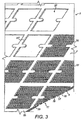
Figure 3 illustrates a fragmentary, sectional perspective view of the stencil ofFigure 1 (illustrated in an inverted orient from the operative orient); and -
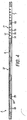
Figure 4 illustrates a vertical sectional view (along section I-I inFigure 1 ) of the stencil ofFigure 1 . -
Figures 1 to 4 illustrate a stencil 3 in accordance with a preferred embodiment of the present invention, mounted in a supporting frame 4, in this embodiment a VectorGuard ® frame (as supplied by DEK). - The stencil 3 comprises an electroformed metal sheet, in this embodiment of solid metal, here of nickel or a nickel alloy. In alternative embodiments the stencil 3 could be formed of other electroformable metals or alloys or combinations thereof.
- As illustrated in
Figures 3 and4 , the stencil 3 comprises a first, upper layer. 5 over which a printing medium is applied in a printing operation, typically using a squeegee or an enclosed print head, and a second, lower layer 7, which overlies a substrate which is to be printed. - In this embodiment the layers 5, 7 of the stencil 3 are integrally formed. In one embodiment the layers 5, 7 are formed of the same material. In another embodiment the layers 5, 7 are formed of different materials.
- The upper layer 5 includes an
apertured region 11, in this embodiment of circular shape, which corresponds in shape and size to the substrate to be printed, and through which printing medium is delivered in a printing operation. It will be understood that theapertured region 11 could have any shape, for example, rectangular. - In this embodiment the
apertured region 11 has the form of a grid, which comprises orthogonally-arrangedweb elements 15, 17, which together defineapertures 19 therebetween, through which printing medium can be delivered. - In this embodiment the
apertures 19 are rectangular, typically square or oblong, but in other embodiments could have different shape, such as circular. - In this embodiment the
web elements 15, 17 have a width of from about 10 µm to about 120 µm, preferably from about 20 µm to about 110 µm, more preferably from about 30 µm to about 100 µm, and more preferably about 30 µm or about 100 µm. - In one embodiment the
web elements 15, 17 have a width of from about 10 µm to about 40 µm, preferably from about 20 µm to about 40 µm, and more preferably about 30 µm. - In another embodiment the
web elements 15, 17 could have a width of from about 80 µm to about 120 µm, preferably from about 90 µm to about 110 µm, and more preferably about 100 µm - In this embodiment the
apertures 19 have an area of at least about 0.001 mm2, preferably from about 0.001 mm2. to about 1 mm2, more preferably at least about 0.0015 mm2, still more preferably from about 0.0015 mm2 to about 1 mm2, yet more preferably at least about 0.0025 mm2, yet still more preferably from about 0.0025 mm2 to about 1 mm2, and still yet more preferably not more than about 0.25 mm2. - In one embodiment the
apertures 19 have side lengths of at least about 50 µm, preferably at least about 100 µm, more preferably at least about 250 µm, and still more preferably not more than about 1 mm. - In this embodiment the upper layer 5 has a thickness of from about 10 µm to about 120 µm, preferably from about 20 µm to about 110 µm, more preferably from about 30 µm to about 100 µm, and still more preferably about 30 µm or about 100 µm.
- In one embodiment the upper layer 5 has a thickness-of from about 20 µm to about 60 µm, preferably from about 20 µm to about 50 µm, more preferably from about 25 µm to about 35 µm, and still more preferably about 30 µm.
- In another embodiment the upper layer 5 has a thickness of from about 80 µm to about 120 µm, preferably from about 90 µm to about 110 µm, and preferably about 100 µm.
- The lower layer 7 includes a plurality of
apertures 31, which each have a pattern corresponding to that to be printed on the substrate. - In this embodiment the
apertures 31 each have a substantially square form, separated by orthogonally-arrangedweb elements apertures 31 could have any desired form. - In this embodiment the
web elements - In this embodiment the
apertures 31 are arranged in the form of a regular array, with theapertures 31 being registered to dies on a substrate, in this embodiment a wafer. - The
apertures 31 repeat laterally beyond theapertured region 11 of the upper layer 5 in anon-apertured region 37. - In this embodiment the
apertures 31 extend laterally beyond theapertured region 11 by a distance of at least about 2 mm, preferably from about 2 mm to about 30 mm, more preferably from about 2 mm to about 20 mm, still more preferably at least about 5 mm, yet more preferably from about 5 mm to about 20 mm, and still more preferably from about 5 mm to about 10 mm. - With this arrangement the
apertures 31 in thenon-apertured region 37 define blind apertures or recesses 31' in the lower surface of the stencil 3. - The present inventors have identified that, by extending the
apertures 31 in the lower layer 7 beyond theapertured region 11 in the upper layer 5 to provide the blind apertures or recesses 31', the stencil 3 provides for significantly improved performance in printing across the entire substrate, and thus significantly-improved yield. - It has been found that, with this configuration, and in one example in the printing of a yellow down-conversion phosphor, the yield is remarkably increased to at least 90%, as compared to yields of about 70% for a stencil of the same design but having no blind apertures recesses 31', and, for some wafers, yields of 99% have been achieved.
- Such is the improvement that it is not necessary to finish the surface of the prints, such as by lapping, to achieve a required thickness and thickness uniformity, or to check the thickness, where printed onto a transfer carrier, prior to transfer onto the dies of a wafer, as are done currently.
Claims (16)
- A stencil (3) for printing a pattern of deposits on a substrate, wherein the stencil (3) comprises an electroformed metal sheet which has a first layer (5) which includes an apertured region (11) through which a printing medium is applied in a printing operation, and a second layer (7) which overlies a substrate to be printed and includes a plurality of apertures (31), wherein the apertures (31) of the second layer (7) extend across and beyond the apertured region (11) in the first layer (5), whereby the second layer (7) includes a plurality of through apertures (31) in registration with the apertured region (11) of the first layer (5), each having a pattern corresponding to that to be printed on the substrate, and a plurality of blind apertures (31') disposed adjacent and outwardly of the apertured region (11) in the first layer (5).
- The stencil (3) of claim 1, wherein the metal sheet is formed of nickel or a nickel alloy.
- The stencil (3) of claim 1 or 2, wherein the layers (5, 7) are integrally formed.
- The stencil (3) of any of claims 1 to 3, wherein the layers (5, 7) are formed of the same material or different materials.
- The stencil (3) of any of claims 1 to 4, wherein the apertured region (11) corresponds in shape and size to the substrate to be printed, optionally the apertured region (11) is circular in shape.
- The stencil (3) of any of claims 1 to 5, wherein the apertured region (11) has the form of a grid which comprises orthogonally-arranged web elements (15, 17), which together define apertures (19) therebetween, optionally the apertures (19) of the first layer (5) are rectangular, optionally the web elements (15, 17) of the first layer (5) have a width of from about 10 µm to about 120 µm, from about 20 µm to about 110 µm, from about 30 µm to about 100 µm, about 30 µm or about 100 µm, optionally the web elements (15, 17) of the first layer (5) have (i) a width of from about 10 µm to about 40 µm, from about 20 µm to about 40 µm or about 30 µm, or (ii) a width of from about 80 µm to about 120 µm, from about 90 µm to about 110 µm or about 100 µm.
- The stencil (3) of any of claims 1 to 6, wherein the apertures (19) of the first layer (5) have an area of at least about 0.001 mm2, from about 0.001 mm2 to about 1 mm2, at least about 0.0015 mm2, from about 0.0015 mm2 to about 1 mm2, at least about 0.0025 mm2, from about 0.0025 mm2 to about 1 mm2 or not more than about 0.25 mm2.
- The stencil (3) of any of claims 1 to 7, wherein the apertures (19) of the first layer (5) have side lengths of at least about 50 µm, at least about 100 µm, at least about 250 µm or not more than about 1 mm.
- The stencil (3) of any of claims 1 to 8, wherein the first layer (5) has a thickness of from about 10 µm to about 120 µm, from about 20 µm to about 110 µm, from about 30 µm to about 100 µm, about 30 µm or about 100 µm, optionally the first layer (5) has (i) a thickness of from about 20 µm to about 60 µm, from about 20 µm to about 50 µm, from about 25 µm to about 35 µm or about 30 µm, or (II) a thickness of from about 80 µm to about 120 µm, from about 90 µm to about 110 µm or about 100 µm.
- The stencil (3) of any of claims 1 to 9, wherein the apertures (31) in the second layer (7) each have a substantially square form, separated by orthogonally-arranged web elements (33, 35), optionally the web elements (33, 35) of the second layer (7) have a width of from about 100 µm to about 200 µm or from about 100 µm to about 150 µm.
- The stencil (3) of any of claims 1 to 10, wherein the apertures (31) in the second layer (7) are arranged In the form of a regular array, optionally the apertures (31) in the second layer (7) repeat laterally outwardly beyond the apertured region (11) of the first layer (5).
- The stencil (3) of any of claims 1 to 11, wherein the apertures (31) of the second layer (7) extend laterally beyond the apertured region (11) of the first layer (5) by a distance of at least about 2 mm, from about 2 mm to about 30 mm, from about 2 mm to about 20 mm, at least about 5 mm, from about 5 mm to about 20 mm or from about 5 mm to about 10 mm.
- The stencil (3) of any of claims 1 to 12, wherein the substrate is a wafer, optionally a silicon or sapphire wafer, or a transfer carrier for transferring the prints to a wafer, optionally a silicon or sapphire wafer.
- A method of printing substrates with a pattern of deposits using the stencil (3) of any of claims 1 to 13, optionally the method is for printing deposits of a phosphor, a down-conversion phosphor on a substrate or a yellow down-conversion phosphor on a substrate.
- The method of claim 14, comprising the steps of:providing a substrate;providing the stencil (3) of any of claims 1 to 13 over the substrate;applying print medium over the stencil (3), such that the print medium is forced through the apertures (31) in the second layer (7) and a pattern of deposits is printed on the substrate corresponding to the pattern of through apertures (31) in the second layer (7) of the stencil;optionally the substrate is a wafer, optionally a silicon or sapphire wafer, and the deposits are printed directly onto dies formed in the wafer without any intermediate transfer steps.
- A method of fabricating a light-emitting device, comprising the steps of:performing the method of claim 15 in which the substrate is a wafer; andseparating the printed dies of the wafer;optionally at least 90% of the printed dies of the wafer are selected,optionally the deposits on the selected dies of the wafer are not subjected to any surface thickness processing, and further comprising the step of:providing each of the selected dies in device packaging to provide light-emitting devices.
Applications Claiming Priority (2)
| Application Number | Priority Date | Filing Date | Title |
|---|---|---|---|
| US201161579766P | 2011-12-23 | 2011-12-23 | |
| PCT/EP2012/076489 WO2013092914A1 (en) | 2011-12-23 | 2012-12-20 | Stencils |
Publications (2)
| Publication Number | Publication Date |
|---|---|
| EP2794282A1 EP2794282A1 (en) | 2014-10-29 |
| EP2794282B1 true EP2794282B1 (en) | 2016-05-18 |
Family
ID=47557096
Family Applications (1)
| Application Number | Title | Priority Date | Filing Date |
|---|---|---|---|
| EP12813853.4A Not-in-force EP2794282B1 (en) | 2011-12-23 | 2012-12-20 | Stencils |
Country Status (5)
| Country | Link |
|---|---|
| US (1) | US10357961B2 (en) |
| EP (1) | EP2794282B1 (en) |
| MY (1) | MY176453A (en) |
| TW (1) | TWI633819B (en) |
| WO (1) | WO2013092914A1 (en) |
Family Cites Families (8)
| Publication number | Priority date | Publication date | Assignee | Title |
|---|---|---|---|---|
| US5361695A (en) * | 1991-07-08 | 1994-11-08 | Danippon Screen Mfg. Co., Ltd. | Screen printing plate for limiting the spread of ink on an object |
| KR19990036273A (en) * | 1996-06-11 | 1999-05-25 | 엠. 제이. 엠. 반캄 | A method of providing a track on a flat substrate by a stencil printing method |
| US6722275B2 (en) * | 2001-09-28 | 2004-04-20 | Photo Stencil, Llc | Reservoir stencil with relief areas and method of using |
| US7514867B2 (en) * | 2004-04-19 | 2009-04-07 | Panasonic Corporation | LED lamp provided with optical diffusion layer having increased thickness and method of manufacturing thereof |
| JP2006156837A (en) * | 2004-11-30 | 2006-06-15 | Matsushita Electric Ind Co Ltd | Semiconductor light emitting device, light emitting module, and lighting device |
| GB2476925A (en) * | 2009-09-21 | 2011-07-20 | Dtg Int Gmbh | Printing screens and method of fabricating the same |
| TW201127554A (en) * | 2010-02-11 | 2011-08-16 | Tian-Yuan Yan | Resin bonding pad conditioner with surface recessed pattern and manufacture method thereof |
| US9331189B2 (en) * | 2012-05-09 | 2016-05-03 | University of Pittsburgh—of the Commonwealth System of Higher Education | Low voltage nanoscale vacuum electronic devices |
-
2012
- 2012-11-30 TW TW101144980A patent/TWI633819B/en active
- 2012-12-20 MY MYPI2014001867A patent/MY176453A/en unknown
- 2012-12-20 US US14/368,242 patent/US10357961B2/en active Active
- 2012-12-20 EP EP12813853.4A patent/EP2794282B1/en not_active Not-in-force
- 2012-12-20 WO PCT/EP2012/076489 patent/WO2013092914A1/en not_active Ceased
Also Published As
| Publication number | Publication date |
|---|---|
| WO2013092914A1 (en) | 2013-06-27 |
| EP2794282A1 (en) | 2014-10-29 |
| TW201345350A (en) | 2013-11-01 |
| US20150165756A1 (en) | 2015-06-18 |
| MY176453A (en) | 2020-08-10 |
| HK1203458A1 (en) | 2016-01-08 |
| TWI633819B (en) | 2018-08-21 |
| US20160001545A9 (en) | 2016-01-07 |
| US10357961B2 (en) | 2019-07-23 |
Similar Documents
| Publication | Publication Date | Title |
|---|---|---|
| US7513194B2 (en) | Screen mask | |
| US8802487B2 (en) | Silk-screen stencil for printing onto a photovoltaic cell | |
| CN110637503A (en) | Method for printing structured silver coatings with improved current carrying capacity | |
| NL2012563B1 (en) | Solar cell module and method manufacturing such a module. | |
| US10357961B2 (en) | Stencils | |
| HK1203458B (en) | Stencils | |
| CN110265563B (en) | Substrate for ink-jet printing light-emitting layer thereon, light-emitting device, and method for producing substrate | |
| US9718267B2 (en) | Screen printing apparatus including support bars, and methods of using same | |
| JP5981276B2 (en) | Screen printing machine and screen printing method | |
| KR20170129342A (en) | Wafer Level Chip Scale Light Emitting Diode Package and Method of Manufacturing the Same | |
| TWI472631B (en) | Shadow mask strip | |
| KR102759948B1 (en) | Metal substrate, metal mask for deposition, and method for manufacturing of the same | |
| US9691946B2 (en) | Method for producing a conversion lamina and conversion lamina | |
| US6662718B2 (en) | Screening mask having a stress-relieving area | |
| US8807025B2 (en) | Mesh for screen printing and method of forming patterns using the mesh for screen printing | |
| JP5256543B2 (en) | Ceramic substrate for chip component and method for manufacturing chip component | |
| TWI689122B (en) | Mask | |
| JPWO2024232066A5 (en) | ||
| CN117202692B (en) | Organic electroluminescent device and manufacturing method thereof, and display panel | |
| KR102739732B1 (en) | Composite frame element for OLED deposition process | |
| JP2012200978A (en) | Printing plate and printing device including the printing plate | |
| KR20110061816A (en) | Manufacturing method of LED package and LED package | |
| KR100930174B1 (en) | Color printing method of metal sticker | |
| CN116770226A (en) | Evaporation mask plate | |
| US20090120310A1 (en) | Printing screens |
Legal Events
| Date | Code | Title | Description |
|---|---|---|---|
| PUAI | Public reference made under article 153(3) epc to a published international application that has entered the european phase |
Free format text: ORIGINAL CODE: 0009012 |
|
| 17P | Request for examination filed |
Effective date: 20140616 |
|
| AK | Designated contracting states |
Kind code of ref document: A1 Designated state(s): AL AT BE BG CH CY CZ DE DK EE ES FI FR GB GR HR HU IE IS IT LI LT LU LV MC MK MT NL NO PL PT RO RS SE SI SK SM TR |
|
| DAX | Request for extension of the european patent (deleted) | ||
| GRAP | Despatch of communication of intention to grant a patent |
Free format text: ORIGINAL CODE: EPIDOSNIGR1 |
|
| RIC1 | Information provided on ipc code assigned before grant |
Ipc: B41M 1/12 20060101ALI20150421BHEP Ipc: B41N 1/24 20060101AFI20150421BHEP |
|
| INTG | Intention to grant announced |
Effective date: 20150512 |
|
| GRAP | Despatch of communication of intention to grant a patent |
Free format text: ORIGINAL CODE: EPIDOSNIGR1 |
|
| RAP1 | Party data changed (applicant data changed or rights of an application transferred) |
Owner name: ASM ASSEMBLY SYSTEMS SWITZERLAND GMBH |
|
| INTG | Intention to grant announced |
Effective date: 20151014 |
|
| REG | Reference to a national code |
Ref country code: HK Ref legal event code: DE Ref document number: 1203458 Country of ref document: HK |
|
| GRAS | Grant fee paid |
Free format text: ORIGINAL CODE: EPIDOSNIGR3 |
|
| GRAA | (expected) grant |
Free format text: ORIGINAL CODE: 0009210 |
|
| AK | Designated contracting states |
Kind code of ref document: B1 Designated state(s): AL AT BE BG CH CY CZ DE DK EE ES FI FR GB GR HR HU IE IS IT LI LT LU LV MC MK MT NL NO PL PT RO RS SE SI SK SM TR |
|
| REG | Reference to a national code |
Ref country code: GB Ref legal event code: FG4D |
|
| REG | Reference to a national code |
Ref country code: CH Ref legal event code: EP |
|
| REG | Reference to a national code |
Ref country code: IE Ref legal event code: FG4D Ref country code: AT Ref legal event code: REF Ref document number: 800088 Country of ref document: AT Kind code of ref document: T Effective date: 20160615 |
|
| REG | Reference to a national code |
Ref country code: DE Ref legal event code: R096 Ref document number: 602012018764 Country of ref document: DE |
|
| REG | Reference to a national code |
Ref country code: NL Ref legal event code: MP Effective date: 20160518 |
|
| REG | Reference to a national code |
Ref country code: LT Ref legal event code: MG4D |
|
| PG25 | Lapsed in a contracting state [announced via postgrant information from national office to epo] |
Ref country code: NL Free format text: LAPSE BECAUSE OF FAILURE TO SUBMIT A TRANSLATION OF THE DESCRIPTION OR TO PAY THE FEE WITHIN THE PRESCRIBED TIME-LIMIT Effective date: 20160518 Ref country code: LT Free format text: LAPSE BECAUSE OF FAILURE TO SUBMIT A TRANSLATION OF THE DESCRIPTION OR TO PAY THE FEE WITHIN THE PRESCRIBED TIME-LIMIT Effective date: 20160518 Ref country code: NO Free format text: LAPSE BECAUSE OF FAILURE TO SUBMIT A TRANSLATION OF THE DESCRIPTION OR TO PAY THE FEE WITHIN THE PRESCRIBED TIME-LIMIT Effective date: 20160818 Ref country code: FI Free format text: LAPSE BECAUSE OF FAILURE TO SUBMIT A TRANSLATION OF THE DESCRIPTION OR TO PAY THE FEE WITHIN THE PRESCRIBED TIME-LIMIT Effective date: 20160518 |
|
| REG | Reference to a national code |
Ref country code: AT Ref legal event code: MK05 Ref document number: 800088 Country of ref document: AT Kind code of ref document: T Effective date: 20160518 |
|
| PG25 | Lapsed in a contracting state [announced via postgrant information from national office to epo] |
Ref country code: RS Free format text: LAPSE BECAUSE OF FAILURE TO SUBMIT A TRANSLATION OF THE DESCRIPTION OR TO PAY THE FEE WITHIN THE PRESCRIBED TIME-LIMIT Effective date: 20160518 Ref country code: PT Free format text: LAPSE BECAUSE OF FAILURE TO SUBMIT A TRANSLATION OF THE DESCRIPTION OR TO PAY THE FEE WITHIN THE PRESCRIBED TIME-LIMIT Effective date: 20160919 Ref country code: LV Free format text: LAPSE BECAUSE OF FAILURE TO SUBMIT A TRANSLATION OF THE DESCRIPTION OR TO PAY THE FEE WITHIN THE PRESCRIBED TIME-LIMIT Effective date: 20160518 Ref country code: ES Free format text: LAPSE BECAUSE OF FAILURE TO SUBMIT A TRANSLATION OF THE DESCRIPTION OR TO PAY THE FEE WITHIN THE PRESCRIBED TIME-LIMIT Effective date: 20160518 Ref country code: SE Free format text: LAPSE BECAUSE OF FAILURE TO SUBMIT A TRANSLATION OF THE DESCRIPTION OR TO PAY THE FEE WITHIN THE PRESCRIBED TIME-LIMIT Effective date: 20160518 Ref country code: GR Free format text: LAPSE BECAUSE OF FAILURE TO SUBMIT A TRANSLATION OF THE DESCRIPTION OR TO PAY THE FEE WITHIN THE PRESCRIBED TIME-LIMIT Effective date: 20160819 Ref country code: HR Free format text: LAPSE BECAUSE OF FAILURE TO SUBMIT A TRANSLATION OF THE DESCRIPTION OR TO PAY THE FEE WITHIN THE PRESCRIBED TIME-LIMIT Effective date: 20160518 |
|
| REG | Reference to a national code |
Ref country code: FR Ref legal event code: PLFP Year of fee payment: 5 |
|
| PG25 | Lapsed in a contracting state [announced via postgrant information from national office to epo] |
Ref country code: IT Free format text: LAPSE BECAUSE OF FAILURE TO SUBMIT A TRANSLATION OF THE DESCRIPTION OR TO PAY THE FEE WITHIN THE PRESCRIBED TIME-LIMIT Effective date: 20160518 |
|
| REG | Reference to a national code |
Ref country code: HK Ref legal event code: GR Ref document number: 1203458 Country of ref document: HK |
|
| PG25 | Lapsed in a contracting state [announced via postgrant information from national office to epo] |
Ref country code: DK Free format text: LAPSE BECAUSE OF FAILURE TO SUBMIT A TRANSLATION OF THE DESCRIPTION OR TO PAY THE FEE WITHIN THE PRESCRIBED TIME-LIMIT Effective date: 20160518 Ref country code: RO Free format text: LAPSE BECAUSE OF FAILURE TO SUBMIT A TRANSLATION OF THE DESCRIPTION OR TO PAY THE FEE WITHIN THE PRESCRIBED TIME-LIMIT Effective date: 20160518 Ref country code: EE Free format text: LAPSE BECAUSE OF FAILURE TO SUBMIT A TRANSLATION OF THE DESCRIPTION OR TO PAY THE FEE WITHIN THE PRESCRIBED TIME-LIMIT Effective date: 20160518 Ref country code: CZ Free format text: LAPSE BECAUSE OF FAILURE TO SUBMIT A TRANSLATION OF THE DESCRIPTION OR TO PAY THE FEE WITHIN THE PRESCRIBED TIME-LIMIT Effective date: 20160518 Ref country code: SK Free format text: LAPSE BECAUSE OF FAILURE TO SUBMIT A TRANSLATION OF THE DESCRIPTION OR TO PAY THE FEE WITHIN THE PRESCRIBED TIME-LIMIT Effective date: 20160518 |
|
| REG | Reference to a national code |
Ref country code: DE Ref legal event code: R097 Ref document number: 602012018764 Country of ref document: DE |
|
| PG25 | Lapsed in a contracting state [announced via postgrant information from national office to epo] |
Ref country code: SM Free format text: LAPSE BECAUSE OF FAILURE TO SUBMIT A TRANSLATION OF THE DESCRIPTION OR TO PAY THE FEE WITHIN THE PRESCRIBED TIME-LIMIT Effective date: 20160518 Ref country code: BE Free format text: LAPSE BECAUSE OF FAILURE TO SUBMIT A TRANSLATION OF THE DESCRIPTION OR TO PAY THE FEE WITHIN THE PRESCRIBED TIME-LIMIT Effective date: 20160518 Ref country code: PL Free format text: LAPSE BECAUSE OF FAILURE TO SUBMIT A TRANSLATION OF THE DESCRIPTION OR TO PAY THE FEE WITHIN THE PRESCRIBED TIME-LIMIT Effective date: 20160518 Ref country code: AT Free format text: LAPSE BECAUSE OF FAILURE TO SUBMIT A TRANSLATION OF THE DESCRIPTION OR TO PAY THE FEE WITHIN THE PRESCRIBED TIME-LIMIT Effective date: 20160518 |
|
| PLBE | No opposition filed within time limit |
Free format text: ORIGINAL CODE: 0009261 |
|
| STAA | Information on the status of an ep patent application or granted ep patent |
Free format text: STATUS: NO OPPOSITION FILED WITHIN TIME LIMIT |
|
| 26N | No opposition filed |
Effective date: 20170221 |
|
| PG25 | Lapsed in a contracting state [announced via postgrant information from national office to epo] |
Ref country code: SI Free format text: LAPSE BECAUSE OF FAILURE TO SUBMIT A TRANSLATION OF THE DESCRIPTION OR TO PAY THE FEE WITHIN THE PRESCRIBED TIME-LIMIT Effective date: 20160518 |
|
| PG25 | Lapsed in a contracting state [announced via postgrant information from national office to epo] |
Ref country code: MC Free format text: LAPSE BECAUSE OF FAILURE TO SUBMIT A TRANSLATION OF THE DESCRIPTION OR TO PAY THE FEE WITHIN THE PRESCRIBED TIME-LIMIT Effective date: 20160518 |
|
| REG | Reference to a national code |
Ref country code: CH Ref legal event code: PL |
|
| REG | Reference to a national code |
Ref country code: DE Ref legal event code: R082 Ref document number: 602012018764 Country of ref document: DE Representative=s name: BECKER-KURIG-STRAUS PATENTANWAELTE PARTNERSCHA, DE Ref country code: DE Ref legal event code: R082 Ref document number: 602012018764 Country of ref document: DE Representative=s name: 2K PATENT- UND RECHTSANWAELTE PARTNERSCHAFT MB, DE Ref country code: DE Ref legal event code: R082 Ref document number: 602012018764 Country of ref document: DE Representative=s name: BECKER, KURIG, STRAUS, DE Ref country code: DE Ref legal event code: R081 Ref document number: 602012018764 Country of ref document: DE Owner name: ASM ASSEMBLY SYSTEMS SINGAPORE PTE LTD., SG Free format text: FORMER OWNER: ASM ASSEMBLY SYSTEMS SWITZERLAND GMBH, ZUERICH, CH |
|
| REG | Reference to a national code |
Ref country code: GB Ref legal event code: 732E Free format text: REGISTERED BETWEEN 20170817 AND 20170823 |
|
| REG | Reference to a national code |
Ref country code: IE Ref legal event code: MM4A |
|
| PG25 | Lapsed in a contracting state [announced via postgrant information from national office to epo] |
Ref country code: LI Free format text: LAPSE BECAUSE OF NON-PAYMENT OF DUE FEES Effective date: 20161231 Ref country code: LU Free format text: LAPSE BECAUSE OF NON-PAYMENT OF DUE FEES Effective date: 20161220 Ref country code: CH Free format text: LAPSE BECAUSE OF NON-PAYMENT OF DUE FEES Effective date: 20161231 |
|
| PG25 | Lapsed in a contracting state [announced via postgrant information from national office to epo] |
Ref country code: IE Free format text: LAPSE BECAUSE OF NON-PAYMENT OF DUE FEES Effective date: 20161220 |
|
| REG | Reference to a national code |
Ref country code: FR Ref legal event code: PLFP Year of fee payment: 6 |
|
| REG | Reference to a national code |
Ref country code: FR Ref legal event code: TP Owner name: ASM ASSEMBLY SYSTEMS SINGAPORE PTE. LTD., SG Effective date: 20171127 |
|
| PG25 | Lapsed in a contracting state [announced via postgrant information from national office to epo] |
Ref country code: HU Free format text: LAPSE BECAUSE OF FAILURE TO SUBMIT A TRANSLATION OF THE DESCRIPTION OR TO PAY THE FEE WITHIN THE PRESCRIBED TIME-LIMIT; INVALID AB INITIO Effective date: 20121220 |
|
| PG25 | Lapsed in a contracting state [announced via postgrant information from national office to epo] |
Ref country code: MK Free format text: LAPSE BECAUSE OF FAILURE TO SUBMIT A TRANSLATION OF THE DESCRIPTION OR TO PAY THE FEE WITHIN THE PRESCRIBED TIME-LIMIT Effective date: 20160518 Ref country code: CY Free format text: LAPSE BECAUSE OF FAILURE TO SUBMIT A TRANSLATION OF THE DESCRIPTION OR TO PAY THE FEE WITHIN THE PRESCRIBED TIME-LIMIT Effective date: 20160518 Ref country code: IS Free format text: LAPSE BECAUSE OF FAILURE TO SUBMIT A TRANSLATION OF THE DESCRIPTION OR TO PAY THE FEE WITHIN THE PRESCRIBED TIME-LIMIT Effective date: 20160518 |
|
| PG25 | Lapsed in a contracting state [announced via postgrant information from national office to epo] |
Ref country code: BG Free format text: LAPSE BECAUSE OF FAILURE TO SUBMIT A TRANSLATION OF THE DESCRIPTION OR TO PAY THE FEE WITHIN THE PRESCRIBED TIME-LIMIT Effective date: 20160518 |
|
| PG25 | Lapsed in a contracting state [announced via postgrant information from national office to epo] |
Ref country code: MT Free format text: LAPSE BECAUSE OF NON-PAYMENT OF DUE FEES Effective date: 20161220 |
|
| PG25 | Lapsed in a contracting state [announced via postgrant information from national office to epo] |
Ref country code: TR Free format text: LAPSE BECAUSE OF FAILURE TO SUBMIT A TRANSLATION OF THE DESCRIPTION OR TO PAY THE FEE WITHIN THE PRESCRIBED TIME-LIMIT Effective date: 20160518 Ref country code: AL Free format text: LAPSE BECAUSE OF FAILURE TO SUBMIT A TRANSLATION OF THE DESCRIPTION OR TO PAY THE FEE WITHIN THE PRESCRIBED TIME-LIMIT Effective date: 20160518 |
|
| REG | Reference to a national code |
Ref country code: DE Ref legal event code: R082 Ref document number: 602012018764 Country of ref document: DE Representative=s name: STRAUS, ALEXANDER, DIPL.-CHEM.UNIV. DR.PHIL., DE Ref country code: DE Ref legal event code: R082 Ref document number: 602012018764 Country of ref document: DE Representative=s name: 2K PATENT- UND RECHTSANWAELTE PARTNERSCHAFT MB, DE |
|
| REG | Reference to a national code |
Ref country code: DE Ref legal event code: R081 Ref document number: 602012018764 Country of ref document: DE Owner name: ASMPT SMT SINGAPORE PTE. LTD., SG Free format text: FORMER OWNER: ASM ASSEMBLY SYSTEMS SINGAPORE PTE LTD., SINGAPUR, SG |
|
| P01 | Opt-out of the competence of the unified patent court (upc) registered |
Effective date: 20230530 |
|
| PGFP | Annual fee paid to national office [announced via postgrant information from national office to epo] |
Ref country code: GB Payment date: 20231220 Year of fee payment: 12 |
|
| PGFP | Annual fee paid to national office [announced via postgrant information from national office to epo] |
Ref country code: FR Payment date: 20231221 Year of fee payment: 12 Ref country code: DE Payment date: 20231214 Year of fee payment: 12 |
|
| REG | Reference to a national code |
Ref country code: DE Ref legal event code: R082 Ref document number: 602012018764 Country of ref document: DE Representative=s name: STRAUS, ALEXANDER, DIPL.-CHEM.UNIV. DR.PHIL., DE |
|
| REG | Reference to a national code |
Ref country code: DE Ref legal event code: R119 Ref document number: 602012018764 Country of ref document: DE |
|
| GBPC | Gb: european patent ceased through non-payment of renewal fee |
Effective date: 20241220 |
|
| PG25 | Lapsed in a contracting state [announced via postgrant information from national office to epo] |
Ref country code: DE Free format text: LAPSE BECAUSE OF NON-PAYMENT OF DUE FEES Effective date: 20250701 |
|
| PG25 | Lapsed in a contracting state [announced via postgrant information from national office to epo] |
Ref country code: GB Free format text: LAPSE BECAUSE OF NON-PAYMENT OF DUE FEES Effective date: 20241220 |
|
| PG25 | Lapsed in a contracting state [announced via postgrant information from national office to epo] |
Ref country code: FR Free format text: LAPSE BECAUSE OF NON-PAYMENT OF DUE FEES Effective date: 20241231 |