EP2793536A1 - Chip on film and display device having the same - Google Patents
Chip on film and display device having the same Download PDFInfo
- Publication number
- EP2793536A1 EP2793536A1 EP20130188529 EP13188529A EP2793536A1 EP 2793536 A1 EP2793536 A1 EP 2793536A1 EP 20130188529 EP20130188529 EP 20130188529 EP 13188529 A EP13188529 A EP 13188529A EP 2793536 A1 EP2793536 A1 EP 2793536A1
- Authority
- EP
- European Patent Office
- Prior art keywords
- chip
- layer
- film
- metal layer
- solder resist
- Prior art date
- Legal status (The legal status is an assumption and is not a legal conclusion. Google has not performed a legal analysis and makes no representation as to the accuracy of the status listed.)
- Granted
Links
Images


Classifications
-
- G—PHYSICS
- G09—EDUCATION; CRYPTOGRAPHY; DISPLAY; ADVERTISING; SEALS
- G09F—DISPLAYING; ADVERTISING; SIGNS; LABELS OR NAME-PLATES; SEALS
- G09F9/00—Indicating arrangements for variable information in which the information is built-up on a support by selection or combination of individual elements
-
- H—ELECTRICITY
- H10—SEMICONDUCTOR DEVICES; ELECTRIC SOLID-STATE DEVICES NOT OTHERWISE PROVIDED FOR
- H10W—GENERIC PACKAGES, INTERCONNECTIONS, CONNECTORS OR OTHER CONSTRUCTIONAL DETAILS OF DEVICES COVERED BY CLASS H10
- H10W42/00—Arrangements for protection of devices
- H10W42/121—Arrangements for protection of devices protecting against mechanical damage
-
- H—ELECTRICITY
- H05—ELECTRIC TECHNIQUES NOT OTHERWISE PROVIDED FOR
- H05K—PRINTED CIRCUITS; CASINGS OR CONSTRUCTIONAL DETAILS OF ELECTRIC APPARATUS; MANUFACTURE OF ASSEMBLAGES OF ELECTRICAL COMPONENTS
- H05K1/00—Printed circuits
- H05K1/02—Details
- H05K1/0277—Bendability or stretchability details
- H05K1/028—Bending or folding regions of flexible printed circuits
- H05K1/0281—Reinforcement details thereof
-
- H—ELECTRICITY
- H10—SEMICONDUCTOR DEVICES; ELECTRIC SOLID-STATE DEVICES NOT OTHERWISE PROVIDED FOR
- H10W—GENERIC PACKAGES, INTERCONNECTIONS, CONNECTORS OR OTHER CONSTRUCTIONAL DETAILS OF DEVICES COVERED BY CLASS H10
- H10W70/00—Package substrates; Interposers; Redistribution layers [RDL]
- H10W70/60—Insulating or insulated package substrates; Interposers; Redistribution layers
- H10W70/67—Insulating or insulated package substrates; Interposers; Redistribution layers characterised by their insulating layers or insulating parts
- H10W70/688—Flexible insulating substrates
-
- G—PHYSICS
- G02—OPTICS
- G02F—OPTICAL DEVICES OR ARRANGEMENTS FOR THE CONTROL OF LIGHT BY MODIFICATION OF THE OPTICAL PROPERTIES OF THE MEDIA OF THE ELEMENTS INVOLVED THEREIN; NON-LINEAR OPTICS; FREQUENCY-CHANGING OF LIGHT; OPTICAL LOGIC ELEMENTS; OPTICAL ANALOGUE/DIGITAL CONVERTERS
- G02F1/00—Devices or arrangements for the control of the intensity, colour, phase, polarisation or direction of light arriving from an independent light source, e.g. switching, gating or modulating; Non-linear optics
- G02F1/01—Devices or arrangements for the control of the intensity, colour, phase, polarisation or direction of light arriving from an independent light source, e.g. switching, gating or modulating; Non-linear optics for the control of the intensity, phase, polarisation or colour
- G02F1/13—Devices or arrangements for the control of the intensity, colour, phase, polarisation or direction of light arriving from an independent light source, e.g. switching, gating or modulating; Non-linear optics for the control of the intensity, phase, polarisation or colour based on liquid crystals, e.g. single liquid crystal display cells
- G02F1/133—Constructional arrangements; Operation of liquid crystal cells; Circuit arrangements
- G02F1/1333—Constructional arrangements; Manufacturing methods
- G02F1/1345—Conductors connecting electrodes to cell terminals
- G02F1/13452—Conductors connecting driver circuitry and terminals of panels
-
- H—ELECTRICITY
- H05—ELECTRIC TECHNIQUES NOT OTHERWISE PROVIDED FOR
- H05K—PRINTED CIRCUITS; CASINGS OR CONSTRUCTIONAL DETAILS OF ELECTRIC APPARATUS; MANUFACTURE OF ASSEMBLAGES OF ELECTRICAL COMPONENTS
- H05K1/00—Printed circuits
- H05K1/18—Printed circuits structurally associated with non-printed electric components
- H05K1/189—Printed circuits structurally associated with non-printed electric components characterised by the use of flexible or folded printed circuits
-
- H—ELECTRICITY
- H05—ELECTRIC TECHNIQUES NOT OTHERWISE PROVIDED FOR
- H05K—PRINTED CIRCUITS; CASINGS OR CONSTRUCTIONAL DETAILS OF ELECTRIC APPARATUS; MANUFACTURE OF ASSEMBLAGES OF ELECTRICAL COMPONENTS
- H05K2201/00—Indexing scheme relating to printed circuits covered by H05K1/00
- H05K2201/10—Details of components or other objects attached to or integrated in a printed circuit board
- H05K2201/10007—Types of components
- H05K2201/10128—Display
-
- H—ELECTRICITY
- H05—ELECTRIC TECHNIQUES NOT OTHERWISE PROVIDED FOR
- H05K—PRINTED CIRCUITS; CASINGS OR CONSTRUCTIONAL DETAILS OF ELECTRIC APPARATUS; MANUFACTURE OF ASSEMBLAGES OF ELECTRICAL COMPONENTS
- H05K2201/00—Indexing scheme relating to printed circuits covered by H05K1/00
- H05K2201/10—Details of components or other objects attached to or integrated in a printed circuit board
- H05K2201/10613—Details of electrical connections of non-printed components, e.g. special leads
- H05K2201/10621—Components characterised by their electrical contacts
- H05K2201/10681—Tape Carrier Package [TCP]; Flexible sheet connector
-
- H—ELECTRICITY
- H05—ELECTRIC TECHNIQUES NOT OTHERWISE PROVIDED FOR
- H05K—PRINTED CIRCUITS; CASINGS OR CONSTRUCTIONAL DETAILS OF ELECTRIC APPARATUS; MANUFACTURE OF ASSEMBLAGES OF ELECTRICAL COMPONENTS
- H05K2201/00—Indexing scheme relating to printed circuits covered by H05K1/00
- H05K2201/20—Details of printed circuits not provided for in H05K2201/01 - H05K2201/10
- H05K2201/2009—Reinforced areas, e.g. for a specific part of a flexible printed circuit
-
- H—ELECTRICITY
- H05—ELECTRIC TECHNIQUES NOT OTHERWISE PROVIDED FOR
- H05K—PRINTED CIRCUITS; CASINGS OR CONSTRUCTIONAL DETAILS OF ELECTRIC APPARATUS; MANUFACTURE OF ASSEMBLAGES OF ELECTRICAL COMPONENTS
- H05K2203/00—Indexing scheme relating to apparatus or processes for manufacturing printed circuits covered by H05K3/00
- H05K2203/05—Patterning and lithography; Masks; Details of resist
- H05K2203/0562—Details of resist
- H05K2203/0577—Double layer of resist having the same pattern
-
- H—ELECTRICITY
- H05—ELECTRIC TECHNIQUES NOT OTHERWISE PROVIDED FOR
- H05K—PRINTED CIRCUITS; CASINGS OR CONSTRUCTIONAL DETAILS OF ELECTRIC APPARATUS; MANUFACTURE OF ASSEMBLAGES OF ELECTRICAL COMPONENTS
- H05K3/00—Apparatus or processes for manufacturing printed circuits
- H05K3/30—Assembling printed circuits with electric components, e.g. with resistors
- H05K3/32—Assembling printed circuits with electric components, e.g. with resistors electrically connecting electric components or wires to printed circuits
- H05K3/34—Assembling printed circuits with electric components, e.g. with resistors electrically connecting electric components or wires to printed circuits by soldering
- H05K3/3452—Solder masks
-
- H—ELECTRICITY
- H10—SEMICONDUCTOR DEVICES; ELECTRIC SOLID-STATE DEVICES NOT OTHERWISE PROVIDED FOR
- H10W—GENERIC PACKAGES, INTERCONNECTIONS, CONNECTORS OR OTHER CONSTRUCTIONAL DETAILS OF DEVICES COVERED BY CLASS H10
- H10W74/00—Encapsulations, e.g. protective coatings
- H10W74/10—Encapsulations, e.g. protective coatings characterised by their shape or disposition
- H10W74/15—Encapsulations, e.g. protective coatings characterised by their shape or disposition on active surfaces of flip-chip devices, e.g. underfills
-
- H—ELECTRICITY
- H10—SEMICONDUCTOR DEVICES; ELECTRIC SOLID-STATE DEVICES NOT OTHERWISE PROVIDED FOR
- H10W—GENERIC PACKAGES, INTERCONNECTIONS, CONNECTORS OR OTHER CONSTRUCTIONAL DETAILS OF DEVICES COVERED BY CLASS H10
- H10W90/00—Package configurations
- H10W90/701—Package configurations characterised by the relative positions of pads or connectors relative to package parts
- H10W90/721—Package configurations characterised by the relative positions of pads or connectors relative to package parts of bump connectors
- H10W90/724—Package configurations characterised by the relative positions of pads or connectors relative to package parts of bump connectors between a chip and a stacked insulating package substrate, interposer or RDL
-
- H—ELECTRICITY
- H10—SEMICONDUCTOR DEVICES; ELECTRIC SOLID-STATE DEVICES NOT OTHERWISE PROVIDED FOR
- H10W—GENERIC PACKAGES, INTERCONNECTIONS, CONNECTORS OR OTHER CONSTRUCTIONAL DETAILS OF DEVICES COVERED BY CLASS H10
- H10W90/00—Package configurations
- H10W90/701—Package configurations characterised by the relative positions of pads or connectors relative to package parts
- H10W90/731—Package configurations characterised by the relative positions of pads or connectors relative to package parts of die-attach connectors
- H10W90/734—Package configurations characterised by the relative positions of pads or connectors relative to package parts of die-attach connectors between a chip and a stacked insulating package substrate, interposer or RDL
Definitions
- the present invention relates to a chip on film and a display device having the same, and more particularly, to a chip on film capable of being prevented from being cracked when the chip on film is bent and a display device having the same.
- display devices that display massive data caused by various electrical signals as images have been extremely developed.
- display devices having advantageous features such as thinner thickness, lighter weight, lower voltage, and lower power consumption
- various display devices e.g., a liquid crystal display device, a plasma display panel device, a field emission display device, an organic electroluminescence display device, etc., have been suggested.
- the above-mentioned flat panel display device includes a display panel that displays the images and a driving circuit board that is connected to a side of the display panel.
- the driving circuit board includes a chip on film having one end portion connected to the display panel and a printed circuit board connected to the other one end portion of the chip on film.
- the chip on film is provided with a data driving integrated circuit chip mounted thereon and the printed circuit board is provided with a base driving integrated circuit chip mounted thereon.
- the driving circuit board applies a driving signal to the display panel to display the images.
- An aspect of the present invention provides a chip on film capable of being prevented from being cracked when the chip on film is bent.
- Another aspect of the present invention provides a display device having the chip on film.
- Embodiments of the present invention provide a flexible chip on film including a base insulating layer, a metal layer disposed on an upper surface of the base insulating layer and including a circuit pattern, an integrated circuit chip disposed on an upper surface of the metal layer and electrically connected to the metal layer, a solder resist layer disposed on the metal layer and insulated from the integrated circuit chip, and a reinforcing layer disposed on an upper surface of the solder resist layer.
- a neutral surface in which a vector sum of a tensile force and a compressive force becomes substantially zero, is placed in the metal layer by the reinforcing layer.
- the solder resist layer includes a cured resin.
- the reinforcing layer has an area equal to or smaller than an area of the solder resist layer and the reinforcing layer has a film shape.
- the reinforcing layer includes a same material as the solder resist layer and is positioned in an area in which the chip on film is bent.
- Embodiments of the present invention provide a display device including a display panel that includes a display area in which an image is displayed and a non-display area disposed adjacent to the display area and a chip on film disposed at one side of the non-display area and having flexibility.
- the chip on film includes a base insulating layer, a metal layer disposed on an upper surface of the base insulating layer and including a circuit pattern, an integrated circuit chip disposed on an upper surface of the metal layer and electrically connected to the metal layer, a solder resist layer disposed on the metal layer and insulated from the integrated circuit chip, and a reinforcing layer disposed on an upper surface of the solder resist layer.
- the chip on film is bent to surround an edge of the non-display area and the integrated circuit chip makes contact with a lower surface of the display panel.
- the solder resist layer includes a cured resin.
- the reinforcing layer has an area equal to or smaller than an area of the solder resist layer and the reinforcing layer has a film shape.
- the reinforcing layer includes a same material as the solder resist layer and is positioned in an area in which the chip on film is bent.
- the reinforcing layer is disposed on the solder resist layer of the chip on film, and thus crack of the metal layer, defect of the chip on film, and defect of the display device may be prevented even though the chip on film is bent.
- the chip on film and the display device may be slimmed and a manufacturing process of the chip on film and the display device may be simplified.
- FIG. 1 is a cross-sectional view showing a chip on film COF according to an exemplary embodiment of the present disclosure.
- the chip on film COF includes a base insulating layer BI, a metal layer ML disposed on an upper surface of the base insulating layer BI, and an integrated circuit chip IC disposed on an upper surface of the metal layer ML and electrically insulated from the metal layer ML.
- the chip on film COF further includes a solder resist layer SR disposed on the metal layer ML and electrically insulated from the integrated circuit chip IC and a reinforcing layer RL disposed on an upper surface of the solder resist layer SR.
- the chip on film COF has flexibility, and thus a neutral surface NP, in which a vector sum of tensile force and compressive force becomes substantially zero when the chip on film COF is bent, is positioned in the chip on film COF.
- the neutral surface NP is positioned in the metal layer ML.
- the base insulating layer BI may be, but not limited to, an insulating film which may be flexibile or rigid.
- the base insulating layer BI includes at least one of polyimide, polyethernitrile, polyethersulfone, polyethyleneterephthalate, polyethylenenaphthalate, and polyvinylchloride.
- the metal layer ML includes a circuit pattern.
- the metal layer ML may be discontinuously provided on the base insulating layer BI. That is, opening areas may exist on the base insulating layer BI in which the metal layer is not provided.
- the metal layer ML includes stainless steel, copper (Cu), iron (Fe), aluminum (Al), or an alloy having at least one of these metals as a main component.
- the metal layer ML may include copper plated with tin (Sn), copper plated with gold (Au), or an alloy having at least one of these metals as a main component.
- a plurality of conductive bumps BMP are disposed at a boundary of the opening areas on the metal layer ML.
- the conductive bumps BMP are adhered to the metal layer ML.
- the integrated circuit chip IC is connected onto the conductive bumps BMP.
- the conductive bumps BMP have a thickness enough to prevent the integrated circuit chip IC from making contact with the solder resist layer SR and the reinforcing layer RL. Consequently, the metal layer ML and the integrated circuit chip IC are electrically connected to each other via the conductive bumps BMP.
- the conductive bumps BMP includes at least one of gold (Au), aluminum (Al), aluminum (Al) alloy, chromium (Cr), chromium (Cr) alloy, molybdenum (Mo), molybdenum (Mo) alloy, silver (Ag), silver (Ag) alloy, copper (Cu), or Nickel (Ni), or an alloy thereof.
- the solder resist layer SR is disposed on the metal layer ML to be spaced apart from the conductive bumps BMP.
- the solder resist layer SR is formed by coating a liquid insulating resin and curing the coated liquid insulating resin.
- the solder resist layer SR prevents conductive foreign substance from directly attaching to the metal layer ML, and thus short circuits may be prevented.
- a thickness of the solder resist SR may be about 5 micrometers to about 25 micrometers.
- An underfill UNF is filled around the integrated circuit chip IC. For instance, a portion of a side surface of the integrated circuit chip IC and a peripheral area of both ends of the metal layer ML are filled with the underfill UNF.
- the underfill UNF is formed by curing a liquid resin and provided to the peripheral area of the integrated circuit chip IC, thereby stably holding the integrated circuit chip IC.
- the underfill UNF improves moisture resistance and mechanical strength of the chip on film COF.
- the reinforcing layer RL has an area equal to or smaller than an area of the solder resist layer SR. When the area of the reinforcing layer RL is smaller than that of the solder resist layer SR, the reinforcing layer RL is spaced apart from the underfilll UNF.
- the reinforcing layer RL has a film shape formed of an organic polymer and is disposed on the solder resist layer SR while interposing an adhesive therebetween.
- the reinforcing layer RL includes at least one of polyimide, polyurethane, or polyethyleneterephthalate.
- the reinforcing layer RL may be formed of the same material as the solder resist layer SR. That is, after the solder resist layer SR is formed by coating the liquid insulating resin and curing the coated liquid insulating resin, the reinforcing layer RL is formed by coating the liquid insulating resin on a predetermined area of the solder resist layer SR again and curing the liquid insulating resin.
- the vector sum of the tensile force and the compressive force becomes substantially zero when the chip on film COF is bent. Accordingly, a deformation rate of the chip on film COF, which is caused by a bending stress applied to the chip on film COF, becomes substantially zero on the neutral surface NP.
- the position of the neutral surface NP is determined in dependence upon thickness and elastic modulus of each of the layers forming the chip on film COF.
- the layers include the base insulating layer BI, the metal layer ML, the solder resist layer SR, and the reinforcing layer RL. That is, when the thickness and the elastic modulus of each layer are changed, the position of the neutral surface NP is shifted, and thus a specific area of the chip on film COF may be prevented from being deformed.
- the metal layer ML is not deformed in the area in which the chip on film COF is bent and the crack does not occur on the metal layer ML even though the bending stress occurs on the chip on film COF, which is caused by the bending of the chip on film COF.
- the thickness and the elastic modulus of the reinforcing layer RL are determined to correspond to the thickness and the elastic modulus of the base insulating layer BI, the metal layer ML, and the solder resist layer SR.
- the reinforcing layer RL is not disposed on the metal layer ML, the neutral surface NP is not positioned in the metal layer ML, but when the reinforcing layer RL is disposed on the metal layer ML, the neutral surface NP is positioned in the metal layer ML.
- the reinforcing layer RL is disposed on the metal layer ML and the neutral surface NP is positioned in the metal layer ML, and thus the metal layer ML may be prevented from being cracked and the defect may be prevented from occurring in the chip on film COF.
- the area of the reinforcing layer RL is smaller than the area of the solder resist layer SR and the reinforcing layer RL is disposed in the area in which the chip on film COF is bent.
- the reinforcing layer RL is additionally disposed on the metal layer ML, the metal layer ML may be prevented from being cracked without increasing the thickness when the chip on film COF is bent.
- a portion of the neutral surface NP may be positioned in the metal layer ML only in the area in which the chip on film COF is bent, and a remaining portion of the neutral surface NP may be positioned at the boundary surface between the metal layer ML and the solder resist layer SR.
- the process required to manufacture the chip on film COF may be simplified. That is, when the similar processes, e.g., the processes of coating and curing the liquid insulating resin, are consecutively performed by varying an area in which the resin is coated, the processes required to form the solder resist layer SR and the reinforcing layer RL are simplified, thereby reducing a manufacturing cost of the solder resist layer SR and the reinforcing layer RL.
- FIG. 2 is a cross-sectional view showing a chip on film according to another exemplary embodiment of the present disclosure.
- the same reference numerals denote the same elements in FIG. 1 , and thus detailed descriptions of the same elements will be omitted.
- a reinforcing layer RL' has an area different from the area of the reinforcing layer RL shown in FIG. 1 .
- the area of the reinforcing layer RL' is equal to the area of the solder resist layer SR. Therefore, the reinforcing layer RL' is not spaced apart from the underfill UNF when viewed in a plan view, and thus a portion of the reinforcing layer RL' is covered by the underfill UNF.
- the neutral surface NP is positioned in the metal layer ML. That is, even though any area of the chip on film COF is bent except for the area in which the integrated circuit chip IC is disposed, the neutral surface NP in the area in which the chip on film COF is bent is always positioned in the metal layer ML, and thus the metal layer ML may be prevented from being cracked.
- a thickness of the solder resist SR may be about 5 micrometers to about 25 micrometers, and a thickness of the reinforcing layer RL is about 30 micrometers to about 40 micrometers.
- FIGS. 3 through 5 the same reference numerals denote the same elements in FIGS. 1 and 2 , and thus detailed descriptions of the same elements will be omitted.
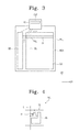
- FIG. 3 is a plan view showing a display device according to an exemplary embodiment of the present disclosure
- FIG. 4 is a circuit diagram showing a pixel area shown in FIG. 3
- FIG. 5 is a cross-sectional view showing a portion of a display device according to an exemplary embodiment of the present disclosure.
- the display device includes a display panel PNL and the chip on film COF that is flexible.
- the display device further includes a housing (not shown) to accommodate the display panel PNL and a window member (not shown) disposed on the display panel PNL to protect the display panel PNL.
- the display panel PNL includes a thin film transistor substrate and a sealing layer (not shown), which are sequentially stacked.
- the display panel PNL includes a thin film transistor substrate and an upper substrate (not shown). In the present exemplary embodiment, only the thin film transistor substrate of the display device PNL has been shown.
- the display panel PNL includes a display area DA in which an image is displayed and a non-display area NDA disposed adjacent to the display area DA.
- the chip on film COF is disposed in the non-display area NDA.
- the display area DA includes a plurality of pixels PXL.
- Each pixel PXL includes a portion of a gate line GL, a portion of a data line DL, a thin film transistor TFT, a pixel electrode PE, an image display layer (not shown), and a common electrode (not shown). These are insulated from each other or make contact with each other.
- the pixels PXL display images to form a full image on a screen of the display panel PNL.
- the gate line GL is extended in a first direction D1 on the thin film transistor substrate in the non-display area NDA and the display area DA.
- the data line DL is extended in a second direction D2 from the non-display area NDA to the display area DA and insulated from the gate line GL.
- the first direction D1 crosses the second direction D2.
- the gate line GL and the data line DL apply signals to the thin film transistor TFT.
- the thin film transistor TFT includes a gate electrode, a semiconductor layer, a source electrode, and a drain electrode.
- the semiconductor layer is disposed on the gate electrode to be insulated from the gate electrode, and a portion of the semiconductor layer is overlapped with the gate electrode.
- the semiconductor layer is formed of an inorganic semiconductor material or an organic semiconductor material.
- the semiconductor layer includes semiconductor, amorphous silicon semiconductor, crystalline silicon semiconductor, or polycrystalline silicon semiconductor.
- the oxide semiconductor includes oxide material including at least one of indium (In), gallium (Ga), zinc (Zn), or tin (Sn).
- the semiconductor layer includes an oxide semiconductor, e.g., zinc oxide, tin oxide, indium oxide, indium-zinc-oxide, indium-tin-oxide, indium-gallium-zinc oxide, indium-zinc-tin oxide, indium-gallium-zinc-tin oxide, etc.
- the image display layer is disposed on a portion of the pixel electrode PE.
- the image display layer includes a light emitting layer.
- the image display layer includes a liquid crystal layer.
- the light emitting layer may include fluorescent materials to emit red, green, and blue colors to respectively correspond to the pixels PXL.
- the pixels that emit the red, green, and blue colors may be referred to as red, green, and blue color pixels respectively corresponding to a red pixel area, a green pixel area, and a blue pixel area.
- red, green, and blue color pixels respectively corresponding to a red pixel area, a green pixel area, and a blue pixel area.
- One red pixel, one green pixel, and one blue pixel form one main pixel, but the color of the light exiting from each pixel PXL, i.e., a wavelength of the light, should not be limited thereto or thereby. That is, each pixel PXL may further emit a yellow light or a magenta light, or one pixel PXL may emit a white light.
- the common electrode is disposed on the image display layer.
- One of the pixel electrode PE and the common electrode is an anode and the other one of the pixel electrode PE and the common electrode is a cathode.
- the sealing layer is disposed on the common electrode to cover the common electrode.
- the non-display area NDA includes a portion of the gate line GL, a portion of the data line DL, a data pad (not shown), and a gate driver GD.
- the data pad and the gate driver GD are connected to the chip on film COF.
- the data pad is extended from the data line DL and covered by the chip on film COF.
- the data pad applies an electrical signal from the chip on film COF to the data line DL.
- the gate driver GD is disposed at one side of the non-display area NDA and applies an electrical signal to the gate line GL.
- the chip on film COF includes the integrated circuit chip IC and the integrated circuit chip IC includes a driver to process the electrical signals applied to the gate driver GD and the data pad.
- the electrical signals are transmitted by various circuit patterns included in the chip on film COF.
- the position and shape of the gate driver GD and the data pad should not be limited thereto or thereby.
- the driver that processes the electrical signals of the display device is provided only in the one side portion of the non-display area NDA in a chip on film scheme or a chip on glass scheme.
- a side portion of the chip on film COF which is not connected to the display panel, may be connected to a printed circuit board.
- the chip on film COF is attached to the side portion of the non-display area NDA using an anisotropic conductive film.
- the metal layer ML of the chip on film COF is attached to the side portion of the non-display area NDA and the solder resist layer SR is not disposed on the area in which the metal layer ML is attached to the side portion of the non-display area NDA.
- the chip on film COF is built in the display device in a bent state to accomplish slimness and compactness. Accordingly, the chip on film COF is bent to surround an edge of the non-display area NDA and the integrated circuit chip IC makes contact with a lower surface of the display panel.
- the integrated circuit chip IC may make contact with the lower surface of the display panel or make contact with the display panel while interposing a bottom cover (not shown) therebetween.
- the chip on film COF includes the base insulating layer BI, the metal layer ML disposed on the upper surface of the base insulating layer BI, and the integrated circuit chip IC disposed on the metal layer ML to be electrically connected to the metal layer ML.
- the chip on film COF further includes the solder resist layer SR disposed on the metal layer ML to be insulated from the integrated circuit chip IC and the reinforcing layer RL disposed on the solder resist layer SR.
- the chip on film COF has flexibility, and thus the neutral surface NP, in which the vector sum of the tensile force and the compressive force becomes substantially zero when the chip on film COF is bent, is positioned in the metal layer ML.
- the thickness and the elastic modulus of the reinforcing layer RL are determined to correspond to the thickness and the elastic modulus of the base insulating layer BI, the metal layer ML, and the solder resist layer SR.
- the reinforcing layer RL is not disposed on the metal layer ML, the neutral surface NP is not positioned in the metal layer ML, but when the reinforcing layer RL is disposed on the metal layer ML, the neutral surface NP is positioned in the metal layer ML.
- the reinforcing layer RL is disposed on the metal layer ML and the neutral surface NP is positioned in the metal layer ML, and thus the metal layer ML may be prevented from being cracked and the defect may be prevented from occurring in the chip on film COF.
- the area of the reinforcing layer RL is smaller than the area of the solder resist layer SR and the reinforcing layer RL is disposed in the area in which the chip on film COF is bent.
- the reinforcing layer RL is additionally disposed on the metal layer ML, the metal layer ML may be prevented from being cracked without increasing the thickness when the chip on film COF is bent.
- a portion of the neutral surface NP may be positioned in the metal layer ML only in the area in which the chip on film COF is bent, and a remaining portion of the neutral surface NP may be positioned at the boundary surface between the metal layer ML and the base insulating layer BI.
- the process required to manufacture the chip on film COF may be simplified. That is, when the similar processes, e.g., the processes of coating and curing the liquid insulating resin, are consecutively performed by varying an area in which the resin is coated, the processes required to form the solder resist layer SR and the reinforcing layer RL are simplified, thereby reducing a manufacturing cost of the solder resist layer SR and the reinforcing layer RL.
- FIG. 6 is a cross-sectional view showing a portion of a display device according to another exemplary embodiment of the present disclosure.
- the same reference numerals denote the same elements in FIGS. 1 through 5 , and thus detailed descriptions of the same elements will be omitted.
- the area of the reinforcing layer RL' is equal to the area of the solder resist layer SR. Therefore, the reinforcing layer RL' is not spaced apart from the underfill UNF when viewed in a plan view, and thus a portion of the reinforcing layer RL' is covered by the underfill UNF.
- the neutral surface NP is positioned in the metal layer ML. That is, even though any area of the chip on film COF is bent except for the area in which the integrated circuit chip IC is disposed, the neutral surface NP in the area in which the chip on film COF is bent is positioned in the metal layer ML, and thus the metal layer ML may be prevented from being cracked.
- a thickness of the solder resist SR may be about 5 micrometers to about 25 micrometers, and a thickness of the reinforcing layer RL' is about 30 micrometers to about 40 micrometers.
Landscapes
- Engineering & Computer Science (AREA)
- Microelectronics & Electronic Packaging (AREA)
- Physics & Mathematics (AREA)
- General Physics & Mathematics (AREA)
- Theoretical Computer Science (AREA)
- Devices For Indicating Variable Information By Combining Individual Elements (AREA)
- Non-Metallic Protective Coatings For Printed Circuits (AREA)
- Structure Of Printed Boards (AREA)
- Liquid Crystal (AREA)
- Wire Bonding (AREA)
Abstract
Description
- The present invention relates to a chip on film and a display device having the same, and more particularly, to a chip on film capable of being prevented from being cracked when the chip on film is bent and a display device having the same.
- In recent years, as the information society has developed rapidly, display devices that display massive data caused by various electrical signals as images have been extremely developed. In particular, as display devices having advantageous features such as thinner thickness, lighter weight, lower voltage, and lower power consumption, various display devices, e.g., a liquid crystal display device, a plasma display panel device, a field emission display device, an organic electroluminescence display device, etc., have been suggested.
- In general, the above-mentioned flat panel display device includes a display panel that displays the images and a driving circuit board that is connected to a side of the display panel. The driving circuit board includes a chip on film having one end portion connected to the display panel and a printed circuit board connected to the other one end portion of the chip on film. The chip on film is provided with a data driving integrated circuit chip mounted thereon and the printed circuit board is provided with a base driving integrated circuit chip mounted thereon. The driving circuit board applies a driving signal to the display panel to display the images.
- An aspect of the present invention provides a chip on film capable of being prevented from being cracked when the chip on film is bent.
Another aspect of the present invention provides a display device having the chip on film. - Embodiments of the present invention provide a flexible chip on film including a base insulating layer, a metal layer disposed on an upper surface of the base insulating layer and including a circuit pattern, an integrated circuit chip disposed on an upper surface of the metal layer and electrically connected to the metal layer, a solder resist layer disposed on the metal layer and insulated from the integrated circuit chip, and a reinforcing layer disposed on an upper surface of the solder resist layer. When the chip on film COF is bent, a neutral surface, in which a vector sum of a tensile force and a compressive force becomes substantially zero, is placed in the metal layer by the reinforcing layer.
- The solder resist layer includes a cured resin.
- The reinforcing layer has an area equal to or smaller than an area of the solder resist layer and the reinforcing layer has a film shape. In addition, the reinforcing layer includes a same material as the solder resist layer and is positioned in an area in which the chip on film is bent.
- Embodiments of the present invention provide a display device including a display panel that includes a display area in which an image is displayed and a non-display area disposed adjacent to the display area and a chip on film disposed at one side of the non-display area and having flexibility.
- The chip on film includes a base insulating layer, a metal layer disposed on an upper surface of the base insulating layer and including a circuit pattern, an integrated circuit chip disposed on an upper surface of the metal layer and electrically connected to the metal layer, a solder resist layer disposed on the metal layer and insulated from the integrated circuit chip, and a reinforcing layer disposed on an upper surface of the solder resist layer. When the chip on film COF is bent, a neutral surface, in which a vector sum of a tensile force and a compressive force becomes substantially zero, is placed in the metal layer by the reinforcing layer.
- The chip on film is bent to surround an edge of the non-display area and the integrated circuit chip makes contact with a lower surface of the display panel.
- The solder resist layer includes a cured resin.
- The reinforcing layer has an area equal to or smaller than an area of the solder resist layer and the reinforcing layer has a film shape. In addition, the reinforcing layer includes a same material as the solder resist layer and is positioned in an area in which the chip on film is bent.
- According to the above, the reinforcing layer is disposed on the solder resist layer of the chip on film, and thus crack of the metal layer, defect of the chip on film, and defect of the display device may be prevented even though the chip on film is bent. In addition, the chip on film and the display device may be slimmed and a manufacturing process of the chip on film and the display device may be simplified.
- A more complete appreciation of the invention, and many of the attendant advantages thereof, will be readily apparent as the same becomes better understood by reference to the following detailed description when considered in conjunction with the accompanying drawings in which like reference symbols indicate the same or similar components, wherein:
-
FIG. 1 is a cross-sectional view showing a chip on film according to an exemplary embodiment of the present disclosure; -
FIG. 2 is a cross-sectional view showing a chip on film according to another exemplary embodiment of the present disclosure; -
FIG. 3 is a plan view showing a display device according to an exemplary embodiment of the present disclosure; -
FIG. 4 is a circuit diagram showing a pixel area shown inFIG. 3 ; -
FIG. 5 is a cross-sectional view showing a portion of a display device according to an exemplary embodiment of the present disclosure; and -
FIG. 6 is a cross-sectional view showing a portion of a display device according to another exemplary embodiment of the present disclosure. -
FIG. 1 is a cross-sectional view showing a chip on film COF according to an exemplary embodiment of the present disclosure.
In reference toFIG. 1 , the chip on film COF includes a base insulating layer BI, a metal layer ML disposed on an upper surface of the base insulating layer BI, and an integrated circuit chip IC disposed on an upper surface of the metal layer ML and electrically insulated from the metal layer ML. In addition, the chip on film COF further includes a solder resist layer SR disposed on the metal layer ML and electrically insulated from the integrated circuit chip IC and a reinforcing layer RL disposed on an upper surface of the solder resist layer SR. - The chip on film COF has flexibility, and thus a neutral surface NP, in which a vector sum of tensile force and compressive force becomes substantially zero when the chip on film COF is bent, is positioned in the chip on film COF. The neutral surface NP is positioned in the metal layer ML.
- The base insulating layer BI may be, but not limited to, an insulating film which may be flexibile or rigid. In detail, the base insulating layer BI includes at least one of polyimide, polyethernitrile, polyethersulfone, polyethyleneterephthalate, polyethylenenaphthalate, and polyvinylchloride.
- The metal layer ML includes a circuit pattern. The metal layer ML may be discontinuously provided on the base insulating layer BI. That is, opening areas may exist on the base insulating layer BI in which the metal layer is not provided.
- The metal layer ML includes stainless steel, copper (Cu), iron (Fe), aluminum (Al), or an alloy having at least one of these metals as a main component. In addition, the metal layer ML may include copper plated with tin (Sn), copper plated with gold (Au), or an alloy having at least one of these metals as a main component.
- A plurality of conductive bumps BMP are disposed at a boundary of the opening areas on the metal layer ML. The conductive bumps BMP are adhered to the metal layer ML. The integrated circuit chip IC is connected onto the conductive bumps BMP. In this case, the conductive bumps BMP have a thickness enough to prevent the integrated circuit chip IC from making contact with the solder resist layer SR and the reinforcing layer RL. Consequently, the metal layer ML and the integrated circuit chip IC are electrically connected to each other via the conductive bumps BMP.
- The conductive bumps BMP includes at least one of gold (Au), aluminum (Al), aluminum (Al) alloy, chromium (Cr), chromium (Cr) alloy, molybdenum (Mo), molybdenum (Mo) alloy, silver (Ag), silver (Ag) alloy, copper (Cu), or Nickel (Ni), or an alloy thereof.
- The solder resist layer SR is disposed on the metal layer ML to be spaced apart from the conductive bumps BMP. The solder resist layer SR is formed by coating a liquid insulating resin and curing the coated liquid insulating resin. The solder resist layer SR prevents conductive foreign substance from directly attaching to the metal layer ML, and thus short circuits may be prevented. A thickness of the solder resist SR may be about 5 micrometers to about 25 micrometers.
- An underfill UNF is filled around the integrated circuit chip IC. For instance, a portion of a side surface of the integrated circuit chip IC and a peripheral area of both ends of the metal layer ML are filled with the underfill UNF. The underfill UNF is formed by curing a liquid resin and provided to the peripheral area of the integrated circuit chip IC, thereby stably holding the integrated circuit chip IC. In addition, the underfill UNF improves moisture resistance and mechanical strength of the chip on film COF.
- The reinforcing layer RL has an area equal to or smaller than an area of the solder resist layer SR. When the area of the reinforcing layer RL is smaller than that of the solder resist layer SR, the reinforcing layer RL is spaced apart from the underfilll UNF.
- The reinforcing layer RL has a film shape formed of an organic polymer and is disposed on the solder resist layer SR while interposing an adhesive therebetween. For instance, the reinforcing layer RL includes at least one of polyimide, polyurethane, or polyethyleneterephthalate. The reinforcing layer RL may be formed of the same material as the solder resist layer SR. That is, after the solder resist layer SR is formed by coating the liquid insulating resin and curing the coated liquid insulating resin, the reinforcing layer RL is formed by coating the liquid insulating resin on a predetermined area of the solder resist layer SR again and curing the liquid insulating resin.
- On the neutral surface NP, the vector sum of the tensile force and the compressive force becomes substantially zero when the chip on film COF is bent. Accordingly, a deformation rate of the chip on film COF, which is caused by a bending stress applied to the chip on film COF, becomes substantially zero on the neutral surface NP.
- The position of the neutral surface NP is determined in dependence upon thickness and elastic modulus of each of the layers forming the chip on film COF. The layers include the base insulating layer BI, the metal layer ML, the solder resist layer SR, and the reinforcing layer RL. That is, when the thickness and the elastic modulus of each layer are changed, the position of the neutral surface NP is shifted, and thus a specific area of the chip on film COF may be prevented from being deformed.
- Thus, when the neutral surface NP is positioned in the metal layer ML, the metal layer ML is not deformed in the area in which the chip on film COF is bent and the crack does not occur on the metal layer ML even though the bending stress occurs on the chip on film COF, which is caused by the bending of the chip on film COF.
- To allow the neutral surface NP to be positioned in the metal layer ML, the thickness and the elastic modulus of the reinforcing layer RL are determined to correspond to the thickness and the elastic modulus of the base insulating layer BI, the metal layer ML, and the solder resist layer SR. When the reinforcing layer RL is not disposed on the metal layer ML, the neutral surface NP is not positioned in the metal layer ML, but when the reinforcing layer RL is disposed on the metal layer ML, the neutral surface NP is positioned in the metal layer ML.
- In the present exemplary embodiment, the reinforcing layer RL is disposed on the metal layer ML and the neutral surface NP is positioned in the metal layer ML, and thus the metal layer ML may be prevented from being cracked and the defect may be prevented from occurring in the chip on film COF.
- In the above-mentioned chip on film COF, the area of the reinforcing layer RL is smaller than the area of the solder resist layer SR and the reinforcing layer RL is disposed in the area in which the chip on film COF is bent. In this case, since the reinforcing layer RL is additionally disposed on the metal layer ML, the metal layer ML may be prevented from being cracked without increasing the thickness when the chip on film COF is bent.
- In the chip on film COF, a portion of the neutral surface NP may be positioned in the metal layer ML only in the area in which the chip on film COF is bent, and a remaining portion of the neutral surface NP may be positioned at the boundary surface between the metal layer ML and the solder resist layer SR.
- In addition, when the reinforcing layer RL is formed of the same material as the solder resist layer SR, the process required to manufacture the chip on film COF may be simplified. That is, when the similar processes, e.g., the processes of coating and curing the liquid insulating resin, are consecutively performed by varying an area in which the resin is coated, the processes required to form the solder resist layer SR and the reinforcing layer RL are simplified, thereby reducing a manufacturing cost of the solder resist layer SR and the reinforcing layer RL.
- Hereinafter,
FIG. 2 is a cross-sectional view showing a chip on film according to another exemplary embodiment of the present disclosure. InFIG. 2 , the same reference numerals denote the same elements inFIG. 1 , and thus detailed descriptions of the same elements will be omitted. - In the present exemplary embodiment shown in
FIG. 2 , a reinforcing layer RL' has an area different from the area of the reinforcing layer RL shown inFIG. 1 . The area of the reinforcing layer RL' is equal to the area of the solder resist layer SR. Therefore, the reinforcing layer RL' is not spaced apart from the underfill UNF when viewed in a plan view, and thus a portion of the reinforcing layer RL' is covered by the underfill UNF. - In this case, although the area in which the chip on film COF is bent is changed, the neutral surface NP is positioned in the metal layer ML. That is, even though any area of the chip on film COF is bent except for the area in which the integrated circuit chip IC is disposed, the neutral surface NP in the area in which the chip on film COF is bent is always positioned in the metal layer ML, and thus the metal layer ML may be prevented from being cracked.
- When the reinforcing layer RL' is formed of the same material as the solder resist layer SR, the process of manufacturing the chip on film COF is more simplified and the manufacturing cost of the chip on film COF is reduced. That is, when the similar processes, e.g., the processes of coating and curing the liquid insulating resin, are consecutively performed by varying the area in which the resin is coated, the processes required to form the solder resist layer SR and the reinforcing layer RL are simplified, thereby reducing the manufacturing cost of the chip on film COF including the solder resist layer SR and the reinforcing layer RL. In the present exemplary embodiments shown in
Fig. 2 , a thickness of the solder resist SR may be about 5 micrometers to about 25 micrometers, and a thickness of the reinforcing layer RL is about 30 micrometers to about 40 micrometers. - Hereinafter, a display device according to an exemplary embodiment of the present disclosure will be described in detail with reference to
FIGS. 3 through 5 . InFIGS. 3 through 5 , the same reference numerals denote the same elements inFIGS. 1 and 2 , and thus detailed descriptions of the same elements will be omitted. -
FIG. 3 is a plan view showing a display device according to an exemplary embodiment of the present disclosure,FIG. 4 is a circuit diagram showing a pixel area shown inFIG. 3 , andFIG. 5 is a cross-sectional view showing a portion of a display device according to an exemplary embodiment of the present disclosure. - In reference to
FIG. 3 , the display device includes a display panel PNL and the chip on film COF that is flexible. In addition, the display device further includes a housing (not shown) to accommodate the display panel PNL and a window member (not shown) disposed on the display panel PNL to protect the display panel PNL. - In a case that the display device is an organic electroluminescence display device, the display panel PNL includes a thin film transistor substrate and a sealing layer (not shown), which are sequentially stacked. In a case that the display device is a liquid crystal display device, the display panel PNL includes a thin film transistor substrate and an upper substrate (not shown). In the present exemplary embodiment, only the thin film transistor substrate of the display device PNL has been shown.
- In reference to
FIG. 3 , the display panel PNL includes a display area DA in which an image is displayed and a non-display area NDA disposed adjacent to the display area DA. The chip on film COF is disposed in the non-display area NDA. - In reference to
FIGS. 3 and 4 , the display area DA includes a plurality of pixels PXL. Each pixel PXL includes a portion of a gate line GL, a portion of a data line DL, a thin film transistor TFT, a pixel electrode PE, an image display layer (not shown), and a common electrode (not shown). These are insulated from each other or make contact with each other. The pixels PXL display images to form a full image on a screen of the display panel PNL. - The gate line GL is extended in a first direction D1 on the thin film transistor substrate in the non-display area NDA and the display area DA. The data line DL is extended in a second direction D2 from the non-display area NDA to the display area DA and insulated from the gate line GL. The first direction D1 crosses the second direction D2.
- The gate line GL and the data line DL apply signals to the thin film transistor TFT. The thin film transistor TFT includes a gate electrode, a semiconductor layer, a source electrode, and a drain electrode.
- The semiconductor layer is disposed on the gate electrode to be insulated from the gate electrode, and a portion of the semiconductor layer is overlapped with the gate electrode.
- The semiconductor layer is formed of an inorganic semiconductor material or an organic semiconductor material. For instance, the semiconductor layer includes semiconductor, amorphous silicon semiconductor, crystalline silicon semiconductor, or polycrystalline silicon semiconductor. The oxide semiconductor includes oxide material including at least one of indium (In), gallium (Ga), zinc (Zn), or tin (Sn). For instance, the semiconductor layer includes an oxide semiconductor, e.g., zinc oxide, tin oxide, indium oxide, indium-zinc-oxide, indium-tin-oxide, indium-gallium-zinc oxide, indium-zinc-tin oxide, indium-gallium-zinc-tin oxide, etc.
- The image display layer is disposed on a portion of the pixel electrode PE. When the display device is the organic electroluminescence display device, the image display layer includes a light emitting layer. When the display device is the liquid crystal display device, the image display layer includes a liquid crystal layer.
- The light emitting layer may include fluorescent materials to emit red, green, and blue colors to respectively correspond to the pixels PXL. In this case, the pixels that emit the red, green, and blue colors may be referred to as red, green, and blue color pixels respectively corresponding to a red pixel area, a green pixel area, and a blue pixel area. One red pixel, one green pixel, and one blue pixel form one main pixel, but the color of the light exiting from each pixel PXL, i.e., a wavelength of the light, should not be limited thereto or thereby. That is, each pixel PXL may further emit a yellow light or a magenta light, or one pixel PXL may emit a white light.
- The common electrode is disposed on the image display layer. One of the pixel electrode PE and the common electrode is an anode and the other one of the pixel electrode PE and the common electrode is a cathode.
- The sealing layer is disposed on the common electrode to cover the common electrode.
- The non-display area NDA includes a portion of the gate line GL, a portion of the data line DL, a data pad (not shown), and a gate driver GD. The data pad and the gate driver GD are connected to the chip on film COF.
- The data pad is extended from the data line DL and covered by the chip on film COF. In addition, the data pad applies an electrical signal from the chip on film COF to the data line DL.
- The gate driver GD is disposed at one side of the non-display area NDA and applies an electrical signal to the gate line GL.
- The chip on film COF includes the integrated circuit chip IC and the integrated circuit chip IC includes a driver to process the electrical signals applied to the gate driver GD and the data pad. The electrical signals are transmitted by various circuit patterns included in the chip on film COF.
- The position and shape of the gate driver GD and the data pad should not be limited thereto or thereby. For instance, the driver that processes the electrical signals of the display device is provided only in the one side portion of the non-display area NDA in a chip on film scheme or a chip on glass scheme.
- Although not shown in figures, a side portion of the chip on film COF, which is not connected to the display panel, may be connected to a printed circuit board.
- The chip on film COF is attached to the side portion of the non-display area NDA using an anisotropic conductive film. In detail, the metal layer ML of the chip on film COF is attached to the side portion of the non-display area NDA and the solder resist layer SR is not disposed on the area in which the metal layer ML is attached to the side portion of the non-display area NDA.
- The chip on film COF is built in the display device in a bent state to accomplish slimness and compactness. Accordingly, the chip on film COF is bent to surround an edge of the non-display area NDA and the integrated circuit chip IC makes contact with a lower surface of the display panel. The integrated circuit chip IC may make contact with the lower surface of the display panel or make contact with the display panel while interposing a bottom cover (not shown) therebetween.
- The chip on film COF includes the base insulating layer BI, the metal layer ML disposed on the upper surface of the base insulating layer BI, and the integrated circuit chip IC disposed on the metal layer ML to be electrically connected to the metal layer ML. In addition, the chip on film COF further includes the solder resist layer SR disposed on the metal layer ML to be insulated from the integrated circuit chip IC and the reinforcing layer RL disposed on the solder resist layer SR.
- The chip on film COF has flexibility, and thus the neutral surface NP, in which the vector sum of the tensile force and the compressive force becomes substantially zero when the chip on film COF is bent, is positioned in the metal layer ML.
- To allow the neutral surface NP to be positioned in the metal layer ML, the thickness and the elastic modulus of the reinforcing layer RL are determined to correspond to the thickness and the elastic modulus of the base insulating layer BI, the metal layer ML, and the solder resist layer SR. When the reinforcing layer RL is not disposed on the metal layer ML, the neutral surface NP is not positioned in the metal layer ML, but when the reinforcing layer RL is disposed on the metal layer ML, the neutral surface NP is positioned in the metal layer ML.
- In the present exemplary embodiment, the reinforcing layer RL is disposed on the metal layer ML and the neutral surface NP is positioned in the metal layer ML, and thus the metal layer ML may be prevented from being cracked and the defect may be prevented from occurring in the chip on film COF.
- In the above-mentioned chip on film COF, the area of the reinforcing layer RL is smaller than the area of the solder resist layer SR and the reinforcing layer RL is disposed in the area in which the chip on film COF is bent. In this case, since the reinforcing layer RL is additionally disposed on the metal layer ML, the metal layer ML may be prevented from being cracked without increasing the thickness when the chip on film COF is bent.
- As shown in
FIG. 5 , in the chip on film COF, a portion of the neutral surface NP may be positioned in the metal layer ML only in the area in which the chip on film COF is bent, and a remaining portion of the neutral surface NP may be positioned at the boundary surface between the metal layer ML and the base insulating layer BI. - In addition, when the reinforcing layer RL is formed of the same material as the solder resist layer SR, the process required to manufacture the chip on film COF may be simplified. That is, when the similar processes, e.g., the processes of coating and curing the liquid insulating resin, are consecutively performed by varying an area in which the resin is coated, the processes required to form the solder resist layer SR and the reinforcing layer RL are simplified, thereby reducing a manufacturing cost of the solder resist layer SR and the reinforcing layer RL.
-
FIG. 6 is a cross-sectional view showing a portion of a display device according to another exemplary embodiment of the present disclosure. InFIG. 6 , the same reference numerals denote the same elements inFIGS. 1 through 5 , and thus detailed descriptions of the same elements will be omitted. - In the present exemplary embodiment shown in
FIG. 6 , the area of the reinforcing layer RL' is equal to the area of the solder resist layer SR. Therefore, the reinforcing layer RL' is not spaced apart from the underfill UNF when viewed in a plan view, and thus a portion of the reinforcing layer RL' is covered by the underfill UNF. - In this case, although the area in which the chip on film COF is bent is changed, the neutral surface NP is positioned in the metal layer ML. That is, even though any area of the chip on film COF is bent except for the area in which the integrated circuit chip IC is disposed, the neutral surface NP in the area in which the chip on film COF is bent is positioned in the metal layer ML, and thus the metal layer ML may be prevented from being cracked.
- When the reinforcing layer RL' is formed of the same material as the solder resist layer SR, the process of manufacturing the chip on film COF is more simplified and the manufacturing cost of the chip on film COF is reduced. That is, when the similar processes, e.g., the processes of coating and curing the liquid insulating resin, are consecutively performed by varying the area in which the resin is coated, the processes required to form the solder resist layer SR and the reinforcing layer RL' are simplified, thereby reducing the manufacturing cost of the chip on film COF including the solder resist layer SR and the reinforcing layer RL'. In the present exemplary embodiments shown in
Fig. 6 , a thickness of the solder resist SR may be about 5 micrometers to about 25 micrometers, and a thickness of the reinforcing layer RL' is about 30 micrometers to about 40 micrometers. - Although the exemplary embodiments of the present invention have been described, it is understood that the present invention should not be limited to these exemplary embodiments but various changes and modifications can be made by one ordinary skilled in the art within the scope of the present invention as hereinafter claimed.
Claims (9)
- A flexible chip on film comprising:a base insulating layer;a metal layer disposed on an upper surface of the base insulating layer and including a circuit pattern;an integrated circuit chip disposed on an upper surface of the metal layer and electrically connected to the metal layer;a solder resist layer disposed on the metal layer and electrically insulated from the integrated circuit chip; anda reinforcing layer disposed on an upper surface of the solder resist layer,wherein a neutral surface, in which a vector sum of a tensile force and a compressive force becomes substantially zero when the chip on film COF is bent, is positioned in the metal layer by the reinforcing layer.
- The chip on film of claim 1, wherein the solder resist layer comprises a cured resin.
- The chip on film of claim 1 or 2, wherein the reinforcing layer has an area equal to or smaller than an area of the solder resist layer.
- The chip on film of claim 1, 2 or 3, wherein the reinforcing layer has a film shape.
- The chip on film of any one of the preceding claims, wherein the reinforcing layer comprises the same material as the solder resist layer.
- The chip on film of any one of the preceding claims wherein the reinforcing layer is positioned in an area in which the chip on film is bent.
- The chip on film of any one of the preceding claims, wherein the thickness and the elastic modulus of the reinforcing layer RL correspond to the thickness and the elastic modulus of the base insulating layer BI, the metal layer ML, and the solder resist layer SR.
- A display device comprising:a display panel that includes a display area in which an image is displayed and a non-display area disposed adjacent to the display area; anda flexible chip on film according to any one of the preceding claims disposed at one side of the non-display area.
- The display device of claim 8, wherein the chip on film is bent to surround an edge of the non-display area and the integrated circuit chip makes contact with a lower surface of the display panel.
Applications Claiming Priority (1)
| Application Number | Priority Date | Filing Date | Title |
|---|---|---|---|
| KR1020130041240A KR20140123852A (en) | 2013-04-15 | 2013-04-15 | Chip on film and display device having the same |
Publications (2)
| Publication Number | Publication Date |
|---|---|
| EP2793536A1 true EP2793536A1 (en) | 2014-10-22 |
| EP2793536B1 EP2793536B1 (en) | 2016-09-21 |
Family
ID=49585260
Family Applications (1)
| Application Number | Title | Priority Date | Filing Date |
|---|---|---|---|
| EP13188529.5A Active EP2793536B1 (en) | 2013-04-15 | 2013-10-14 | Chip on film and display device having the same |
Country Status (3)
| Country | Link |
|---|---|
| US (1) | US9583448B2 (en) |
| EP (1) | EP2793536B1 (en) |
| KR (1) | KR20140123852A (en) |
Cited By (3)
| Publication number | Priority date | Publication date | Assignee | Title |
|---|---|---|---|---|
| CN107615158A (en) * | 2015-08-04 | 2018-01-19 | 株式会社藤仓 | Optical devices |
| CN110265524A (en) * | 2019-05-06 | 2019-09-20 | 江苏稳润光电科技有限公司 | A high light efficiency flexible LED filament and packaging method thereof |
| EP3595027A1 (en) * | 2018-07-12 | 2020-01-15 | Samsung Display Co., Ltd. | Display device having a reinforcing layer |
Families Citing this family (26)
| Publication number | Priority date | Publication date | Assignee | Title |
|---|---|---|---|---|
| KR102304102B1 (en) * | 2015-01-14 | 2021-09-23 | 삼성디스플레이 주식회사 | Display device |
| CN106358360B (en) | 2015-07-14 | 2019-07-19 | 财团法人工业技术研究院 | Flexible electronic device and method of making the same |
| CN204884440U (en) * | 2015-08-27 | 2015-12-16 | 京东方科技集团股份有限公司 | Flexible display panel and flexible display device |
| WO2017066896A1 (en) * | 2015-10-23 | 2017-04-27 | 璩泽明 | Electrical connection structure between the front and rear of a chip, and manufacturing method therefor |
| CN105278185A (en) * | 2015-11-19 | 2016-01-27 | 深圳市华星光电技术有限公司 | Liquid crystal screen and gate COF structure assembly and liquid crystal display device |
| KR102532627B1 (en) * | 2016-06-10 | 2023-05-15 | 삼성디스플레이 주식회사 | Cof package and display device comprising the same |
| KR102487061B1 (en) * | 2016-06-30 | 2023-01-12 | 삼성디스플레이 주식회사 | Display device |
| KR102649632B1 (en) * | 2016-09-13 | 2024-03-21 | 삼성디스플레이 주식회사 | Display device |
| KR102420788B1 (en) * | 2017-07-18 | 2022-07-13 | 엘지디스플레이 주식회사 | display device |
| US10777498B2 (en) * | 2017-08-29 | 2020-09-15 | Novatek Microelectronics Corp. | Chip on film package with reinforcing sheet |
| CN107578707B (en) * | 2017-10-20 | 2019-09-27 | 上海天马微电子有限公司 | Flexible display panel and display device |
| KR102515942B1 (en) * | 2017-12-29 | 2023-03-31 | 엘지디스플레이 주식회사 | Foldable Display Having Step Stack Structure |
| KR102769277B1 (en) * | 2019-02-13 | 2025-02-21 | 삼성디스플레이 주식회사 | Display device and manufacturing method thereof |
| KR102543443B1 (en) * | 2019-03-08 | 2023-06-14 | 삼성디스플레이 주식회사 | Display device and method of manufacturing the flexible printed circuit board |
| KR102769973B1 (en) * | 2019-03-20 | 2025-02-19 | 삼성디스플레이 주식회사 | Display device and manufacturing method of the same |
| JP2020177946A (en) * | 2019-04-15 | 2020-10-29 | 東レ・デュポン株式会社 | Film boards, circuit boards, display devices and electronic devices |
| US10999926B2 (en) * | 2019-06-24 | 2021-05-04 | Flex Ltd. | Stress relief encapsulation for flexible hybrid electronics |
| CN110602874B (en) * | 2019-09-18 | 2021-03-30 | 昆山工研院新型平板显示技术中心有限公司 | Flexible circuit board, preparation method thereof and display device |
| CN110957328B (en) * | 2019-11-29 | 2022-07-12 | 武汉华星光电技术有限公司 | Chip-on-Film and Display |
| KR102873066B1 (en) * | 2020-02-19 | 2025-10-16 | 삼성전자주식회사 | Chip-on-film package, and display module and electronic device comprising the same |
| CN113363264B (en) * | 2020-03-05 | 2024-05-17 | 京东方科技集团股份有限公司 | Array substrate, preparation method thereof and display device |
| US11297718B2 (en) * | 2020-06-30 | 2022-04-05 | Gentherm Gmbh | Methods of manufacturing flex circuits with mechanically formed conductive traces |
| CN117238895A (en) | 2021-07-20 | 2023-12-15 | 武汉华星光电半导体显示技术有限公司 | Flexible display panel and display device |
| KR102903019B1 (en) * | 2021-07-26 | 2025-12-22 | 삼성디스플레이 주식회사 | Display device and method of manufacturing of the display device |
| US20230058776A1 (en) * | 2021-08-20 | 2023-02-23 | Samsung Display Co., Ltd. | Display device and method of manufacturing the same |
| CN113990910B (en) * | 2021-10-29 | 2026-01-27 | 京东方科技集团股份有限公司 | Display device |
Citations (4)
| Publication number | Priority date | Publication date | Assignee | Title |
|---|---|---|---|---|
| US20020027634A1 (en) * | 2000-07-20 | 2002-03-07 | Sin-Gu Kang | Liquid crystal display device having a flexible circuit board |
| US20050110049A1 (en) * | 2003-10-27 | 2005-05-26 | Tatsuhiro Urushido | Semiconductor device and its manufacturing method, electronic module, and electronic unit |
| US20050167803A1 (en) * | 2004-02-02 | 2005-08-04 | Matsushita Elec. Ind. Co. Ltd. | Film substrate, fabrication method thereof, and image display substrate |
| US20060060949A1 (en) * | 2004-09-22 | 2006-03-23 | Katsuyuki Naitoh | Semiconductor device, flexible substrate, tape carrier, and electronic device including the semiconductor device |
Family Cites Families (8)
| Publication number | Priority date | Publication date | Assignee | Title |
|---|---|---|---|---|
| JP2005251671A (en) * | 2004-03-08 | 2005-09-15 | Fuji Photo Film Co Ltd | Display device |
| KR100956238B1 (en) * | 2007-12-18 | 2010-05-04 | 삼성전기주식회사 | Flexible printed circuit board and its manufacturing method |
| EP2255378B1 (en) | 2008-03-05 | 2015-08-05 | The Board of Trustees of the University of Illinois | Stretchable and foldable electronic devices |
| EP2747527A1 (en) | 2008-06-30 | 2014-06-25 | Nippon Steel & Sumikin Chemical Co., Ltd. | Flexible circuit board and bend structure and device comprising the flexible circuit board |
| WO2010032780A1 (en) | 2008-09-18 | 2010-03-25 | 古河電気工業株式会社 | Metal clad body, circuit board and electronic part |
| CN101996535A (en) * | 2009-08-25 | 2011-03-30 | 精工爱普生株式会社 | Electro-optical device and electronic apparatus |
| KR101151473B1 (en) | 2009-11-30 | 2012-06-01 | 엘지이노텍 주식회사 | Flexible Printed Circuits Board and Manufacturing method of the same |
| KR101838736B1 (en) * | 2011-12-20 | 2018-03-15 | 삼성전자 주식회사 | Tape wiring substrate and chip on film package including the same |
-
2013
- 2013-04-15 KR KR1020130041240A patent/KR20140123852A/en not_active Ceased
- 2013-09-09 US US14/021,302 patent/US9583448B2/en active Active
- 2013-10-14 EP EP13188529.5A patent/EP2793536B1/en active Active
Patent Citations (4)
| Publication number | Priority date | Publication date | Assignee | Title |
|---|---|---|---|---|
| US20020027634A1 (en) * | 2000-07-20 | 2002-03-07 | Sin-Gu Kang | Liquid crystal display device having a flexible circuit board |
| US20050110049A1 (en) * | 2003-10-27 | 2005-05-26 | Tatsuhiro Urushido | Semiconductor device and its manufacturing method, electronic module, and electronic unit |
| US20050167803A1 (en) * | 2004-02-02 | 2005-08-04 | Matsushita Elec. Ind. Co. Ltd. | Film substrate, fabrication method thereof, and image display substrate |
| US20060060949A1 (en) * | 2004-09-22 | 2006-03-23 | Katsuyuki Naitoh | Semiconductor device, flexible substrate, tape carrier, and electronic device including the semiconductor device |
Cited By (4)
| Publication number | Priority date | Publication date | Assignee | Title |
|---|---|---|---|---|
| CN107615158A (en) * | 2015-08-04 | 2018-01-19 | 株式会社藤仓 | Optical devices |
| EP3595027A1 (en) * | 2018-07-12 | 2020-01-15 | Samsung Display Co., Ltd. | Display device having a reinforcing layer |
| US10943961B2 (en) | 2018-07-12 | 2021-03-09 | Samsung Display Co., Ltd. | Display device having a reinforcing layer |
| CN110265524A (en) * | 2019-05-06 | 2019-09-20 | 江苏稳润光电科技有限公司 | A high light efficiency flexible LED filament and packaging method thereof |
Also Published As
| Publication number | Publication date |
|---|---|
| KR20140123852A (en) | 2014-10-23 |
| EP2793536B1 (en) | 2016-09-21 |
| US20140306348A1 (en) | 2014-10-16 |
| US9583448B2 (en) | 2017-02-28 |
Similar Documents
| Publication | Publication Date | Title |
|---|---|---|
| EP2793536B1 (en) | Chip on film and display device having the same | |
| US10914992B2 (en) | Display apparatus and method of manufacturing the same | |
| CN112310137B (en) | Stretchable display device | |
| CN112310138B (en) | retractable display device | |
| CN112563289B (en) | Stretchable display device | |
| US11436950B2 (en) | Stretchable display device | |
| US11714504B2 (en) | Display device | |
| US12484404B2 (en) | Display device | |
| US20110086451A1 (en) | Flat panel display and method of fabricating the same | |
| US10325534B2 (en) | Display device | |
| TW200930168A (en) | Flexible film and display device comprising the same | |
| US10211271B2 (en) | Organic light emitting display device | |
| JP7478257B2 (en) | Display device | |
| US8576576B2 (en) | Display apparatus and driving chip mounting film in the display apparatus | |
| KR20210053559A (en) | Stretchable display device | |
| US20250365909A1 (en) | Display panel | |
| CN116390583A (en) | display device | |
| US12414252B2 (en) | Display panel and a manufacturing method thereof | |
| KR20140120180A (en) | Bottom emission type organic light emitting display device and manufacturing method of the same | |
| CN116343591A (en) | display panel | |
| CN121174757A (en) | Stretchable display device and method of manufacturing the same | |
| KR20220067487A (en) | Display device | |
| CN114093888A (en) | Display device |
Legal Events
| Date | Code | Title | Description |
|---|---|---|---|
| PUAI | Public reference made under article 153(3) epc to a published international application that has entered the european phase |
Free format text: ORIGINAL CODE: 0009012 |
|
| 17P | Request for examination filed |
Effective date: 20131014 |
|
| AK | Designated contracting states |
Kind code of ref document: A1 Designated state(s): AL AT BE BG CH CY CZ DE DK EE ES FI FR GB GR HR HU IE IS IT LI LT LU LV MC MK MT NL NO PL PT RO RS SE SI SK SM TR |
|
| AX | Request for extension of the european patent |
Extension state: BA ME |
|
| R17P | Request for examination filed (corrected) |
Effective date: 20150223 |
|
| RBV | Designated contracting states (corrected) |
Designated state(s): AL AT BE BG CH CY CZ DE DK EE ES FI FR GB GR HR HU IE IS IT LI LT LU LV MC MK MT NL NO PL PT RO RS SE SI SK SM TR |
|
| RAP1 | Party data changed (applicant data changed or rights of an application transferred) |
Owner name: SAMSUNG DISPLAY CO., LTD. |
|
| GRAP | Despatch of communication of intention to grant a patent |
Free format text: ORIGINAL CODE: EPIDOSNIGR1 |
|
| RIC1 | Information provided on ipc code assigned before grant |
Ipc: H05K 1/18 20060101ALN20160310BHEP Ipc: H01L 23/498 20060101ALI20160310BHEP Ipc: G02F 1/1345 20060101ALN20160310BHEP Ipc: H01L 23/00 20060101ALI20160310BHEP Ipc: H05K 1/02 20060101AFI20160310BHEP Ipc: H05K 3/34 20060101ALN20160310BHEP |
|
| INTG | Intention to grant announced |
Effective date: 20160401 |
|
| GRAS | Grant fee paid |
Free format text: ORIGINAL CODE: EPIDOSNIGR3 |
|
| GRAA | (expected) grant |
Free format text: ORIGINAL CODE: 0009210 |
|
| AK | Designated contracting states |
Kind code of ref document: B1 Designated state(s): AL AT BE BG CH CY CZ DE DK EE ES FI FR GB GR HR HU IE IS IT LI LT LU LV MC MK MT NL NO PL PT RO RS SE SI SK SM TR |
|
| REG | Reference to a national code |
Ref country code: GB Ref legal event code: FG4D |
|
| REG | Reference to a national code |
Ref country code: CH Ref legal event code: EP |
|
| REG | Reference to a national code |
Ref country code: AT Ref legal event code: REF Ref document number: 831958 Country of ref document: AT Kind code of ref document: T Effective date: 20161015 |
|
| REG | Reference to a national code |
Ref country code: IE Ref legal event code: FG4D |
|
| REG | Reference to a national code |
Ref country code: FR Ref legal event code: PLFP Year of fee payment: 4 |
|
| REG | Reference to a national code |
Ref country code: DE Ref legal event code: R096 Ref document number: 602013011791 Country of ref document: DE |
|
| REG | Reference to a national code |
Ref country code: LT Ref legal event code: MG4D Ref country code: NL Ref legal event code: MP Effective date: 20160921 |
|
| PG25 | Lapsed in a contracting state [announced via postgrant information from national office to epo] |
Ref country code: NO Free format text: LAPSE BECAUSE OF FAILURE TO SUBMIT A TRANSLATION OF THE DESCRIPTION OR TO PAY THE FEE WITHIN THE PRESCRIBED TIME-LIMIT Effective date: 20161221 Ref country code: RS Free format text: LAPSE BECAUSE OF FAILURE TO SUBMIT A TRANSLATION OF THE DESCRIPTION OR TO PAY THE FEE WITHIN THE PRESCRIBED TIME-LIMIT Effective date: 20160921 Ref country code: LT Free format text: LAPSE BECAUSE OF FAILURE TO SUBMIT A TRANSLATION OF THE DESCRIPTION OR TO PAY THE FEE WITHIN THE PRESCRIBED TIME-LIMIT Effective date: 20160921 Ref country code: FI Free format text: LAPSE BECAUSE OF FAILURE TO SUBMIT A TRANSLATION OF THE DESCRIPTION OR TO PAY THE FEE WITHIN THE PRESCRIBED TIME-LIMIT Effective date: 20160921 |
|
| REG | Reference to a national code |
Ref country code: AT Ref legal event code: MK05 Ref document number: 831958 Country of ref document: AT Kind code of ref document: T Effective date: 20160921 |
|
| PG25 | Lapsed in a contracting state [announced via postgrant information from national office to epo] |
Ref country code: BE Free format text: LAPSE BECAUSE OF NON-PAYMENT OF DUE FEES Effective date: 20161031 Ref country code: LV Free format text: LAPSE BECAUSE OF FAILURE TO SUBMIT A TRANSLATION OF THE DESCRIPTION OR TO PAY THE FEE WITHIN THE PRESCRIBED TIME-LIMIT Effective date: 20160921 Ref country code: SE Free format text: LAPSE BECAUSE OF FAILURE TO SUBMIT A TRANSLATION OF THE DESCRIPTION OR TO PAY THE FEE WITHIN THE PRESCRIBED TIME-LIMIT Effective date: 20160921 Ref country code: NL Free format text: LAPSE BECAUSE OF FAILURE TO SUBMIT A TRANSLATION OF THE DESCRIPTION OR TO PAY THE FEE WITHIN THE PRESCRIBED TIME-LIMIT Effective date: 20160921 Ref country code: GR Free format text: LAPSE BECAUSE OF FAILURE TO SUBMIT A TRANSLATION OF THE DESCRIPTION OR TO PAY THE FEE WITHIN THE PRESCRIBED TIME-LIMIT Effective date: 20161222 |
|
| PG25 | Lapsed in a contracting state [announced via postgrant information from national office to epo] |
Ref country code: RO Free format text: LAPSE BECAUSE OF FAILURE TO SUBMIT A TRANSLATION OF THE DESCRIPTION OR TO PAY THE FEE WITHIN THE PRESCRIBED TIME-LIMIT Effective date: 20160921 Ref country code: EE Free format text: LAPSE BECAUSE OF FAILURE TO SUBMIT A TRANSLATION OF THE DESCRIPTION OR TO PAY THE FEE WITHIN THE PRESCRIBED TIME-LIMIT Effective date: 20160921 |
|
| PG25 | Lapsed in a contracting state [announced via postgrant information from national office to epo] |
Ref country code: BE Free format text: LAPSE BECAUSE OF FAILURE TO SUBMIT A TRANSLATION OF THE DESCRIPTION OR TO PAY THE FEE WITHIN THE PRESCRIBED TIME-LIMIT Effective date: 20160921 Ref country code: PT Free format text: LAPSE BECAUSE OF FAILURE TO SUBMIT A TRANSLATION OF THE DESCRIPTION OR TO PAY THE FEE WITHIN THE PRESCRIBED TIME-LIMIT Effective date: 20170123 Ref country code: IS Free format text: LAPSE BECAUSE OF FAILURE TO SUBMIT A TRANSLATION OF THE DESCRIPTION OR TO PAY THE FEE WITHIN THE PRESCRIBED TIME-LIMIT Effective date: 20170121 Ref country code: SM Free format text: LAPSE BECAUSE OF FAILURE TO SUBMIT A TRANSLATION OF THE DESCRIPTION OR TO PAY THE FEE WITHIN THE PRESCRIBED TIME-LIMIT Effective date: 20160921 Ref country code: SK Free format text: LAPSE BECAUSE OF FAILURE TO SUBMIT A TRANSLATION OF THE DESCRIPTION OR TO PAY THE FEE WITHIN THE PRESCRIBED TIME-LIMIT Effective date: 20160921 Ref country code: PL Free format text: LAPSE BECAUSE OF FAILURE TO SUBMIT A TRANSLATION OF THE DESCRIPTION OR TO PAY THE FEE WITHIN THE PRESCRIBED TIME-LIMIT Effective date: 20160921 Ref country code: AT Free format text: LAPSE BECAUSE OF FAILURE TO SUBMIT A TRANSLATION OF THE DESCRIPTION OR TO PAY THE FEE WITHIN THE PRESCRIBED TIME-LIMIT Effective date: 20160921 Ref country code: CZ Free format text: LAPSE BECAUSE OF FAILURE TO SUBMIT A TRANSLATION OF THE DESCRIPTION OR TO PAY THE FEE WITHIN THE PRESCRIBED TIME-LIMIT Effective date: 20160921 Ref country code: ES Free format text: LAPSE BECAUSE OF FAILURE TO SUBMIT A TRANSLATION OF THE DESCRIPTION OR TO PAY THE FEE WITHIN THE PRESCRIBED TIME-LIMIT Effective date: 20160921 Ref country code: BG Free format text: LAPSE BECAUSE OF FAILURE TO SUBMIT A TRANSLATION OF THE DESCRIPTION OR TO PAY THE FEE WITHIN THE PRESCRIBED TIME-LIMIT Effective date: 20161221 |
|
| REG | Reference to a national code |
Ref country code: CH Ref legal event code: PL |
|
| REG | Reference to a national code |
Ref country code: DE Ref legal event code: R097 Ref document number: 602013011791 Country of ref document: DE |
|
| PG25 | Lapsed in a contracting state [announced via postgrant information from national office to epo] |
Ref country code: IT Free format text: LAPSE BECAUSE OF FAILURE TO SUBMIT A TRANSLATION OF THE DESCRIPTION OR TO PAY THE FEE WITHIN THE PRESCRIBED TIME-LIMIT Effective date: 20160921 |
|
| REG | Reference to a national code |
Ref country code: IE Ref legal event code: MM4A |
|
| PLBE | No opposition filed within time limit |
Free format text: ORIGINAL CODE: 0009261 |
|
| STAA | Information on the status of an ep patent application or granted ep patent |
Free format text: STATUS: NO OPPOSITION FILED WITHIN TIME LIMIT |
|
| PG25 | Lapsed in a contracting state [announced via postgrant information from national office to epo] |
Ref country code: LI Free format text: LAPSE BECAUSE OF NON-PAYMENT OF DUE FEES Effective date: 20161031 Ref country code: CH Free format text: LAPSE BECAUSE OF NON-PAYMENT OF DUE FEES Effective date: 20161031 Ref country code: DK Free format text: LAPSE BECAUSE OF FAILURE TO SUBMIT A TRANSLATION OF THE DESCRIPTION OR TO PAY THE FEE WITHIN THE PRESCRIBED TIME-LIMIT Effective date: 20160921 |
|
| 26N | No opposition filed |
Effective date: 20170622 |
|
| PG25 | Lapsed in a contracting state [announced via postgrant information from national office to epo] |
Ref country code: LU Free format text: LAPSE BECAUSE OF NON-PAYMENT OF DUE FEES Effective date: 20161014 |
|
| REG | Reference to a national code |
Ref country code: FR Ref legal event code: PLFP Year of fee payment: 5 |
|
| PG25 | Lapsed in a contracting state [announced via postgrant information from national office to epo] |
Ref country code: IE Free format text: LAPSE BECAUSE OF NON-PAYMENT OF DUE FEES Effective date: 20161014 Ref country code: SI Free format text: LAPSE BECAUSE OF FAILURE TO SUBMIT A TRANSLATION OF THE DESCRIPTION OR TO PAY THE FEE WITHIN THE PRESCRIBED TIME-LIMIT Effective date: 20160921 |
|
| PG25 | Lapsed in a contracting state [announced via postgrant information from national office to epo] |
Ref country code: HU Free format text: LAPSE BECAUSE OF FAILURE TO SUBMIT A TRANSLATION OF THE DESCRIPTION OR TO PAY THE FEE WITHIN THE PRESCRIBED TIME-LIMIT; INVALID AB INITIO Effective date: 20131014 |
|
| PG25 | Lapsed in a contracting state [announced via postgrant information from national office to epo] |
Ref country code: MK Free format text: LAPSE BECAUSE OF FAILURE TO SUBMIT A TRANSLATION OF THE DESCRIPTION OR TO PAY THE FEE WITHIN THE PRESCRIBED TIME-LIMIT Effective date: 20160921 Ref country code: MT Free format text: LAPSE BECAUSE OF NON-PAYMENT OF DUE FEES Effective date: 20161031 Ref country code: CY Free format text: LAPSE BECAUSE OF FAILURE TO SUBMIT A TRANSLATION OF THE DESCRIPTION OR TO PAY THE FEE WITHIN THE PRESCRIBED TIME-LIMIT Effective date: 20160921 Ref country code: HR Free format text: LAPSE BECAUSE OF FAILURE TO SUBMIT A TRANSLATION OF THE DESCRIPTION OR TO PAY THE FEE WITHIN THE PRESCRIBED TIME-LIMIT Effective date: 20160921 Ref country code: MC Free format text: LAPSE BECAUSE OF FAILURE TO SUBMIT A TRANSLATION OF THE DESCRIPTION OR TO PAY THE FEE WITHIN THE PRESCRIBED TIME-LIMIT Effective date: 20160921 |
|
| REG | Reference to a national code |
Ref country code: FR Ref legal event code: PLFP Year of fee payment: 6 |
|
| PG25 | Lapsed in a contracting state [announced via postgrant information from national office to epo] |
Ref country code: TR Free format text: LAPSE BECAUSE OF FAILURE TO SUBMIT A TRANSLATION OF THE DESCRIPTION OR TO PAY THE FEE WITHIN THE PRESCRIBED TIME-LIMIT Effective date: 20160921 Ref country code: AL Free format text: LAPSE BECAUSE OF FAILURE TO SUBMIT A TRANSLATION OF THE DESCRIPTION OR TO PAY THE FEE WITHIN THE PRESCRIBED TIME-LIMIT Effective date: 20160921 |
|
| P01 | Opt-out of the competence of the unified patent court (upc) registered |
Effective date: 20230515 |
|
| PGFP | Annual fee paid to national office [announced via postgrant information from national office to epo] |
Ref country code: GB Payment date: 20250922 Year of fee payment: 13 |
|
| PGFP | Annual fee paid to national office [announced via postgrant information from national office to epo] |
Ref country code: FR Payment date: 20250925 Year of fee payment: 13 |
|
| PGFP | Annual fee paid to national office [announced via postgrant information from national office to epo] |
Ref country code: DE Payment date: 20250922 Year of fee payment: 13 |