EP2793137A2 - Semiconductor Device and Processor System including the Same - Google Patents
Semiconductor Device and Processor System including the Same Download PDFInfo
- Publication number
- EP2793137A2 EP2793137A2 EP14161427.1A EP14161427A EP2793137A2 EP 2793137 A2 EP2793137 A2 EP 2793137A2 EP 14161427 A EP14161427 A EP 14161427A EP 2793137 A2 EP2793137 A2 EP 2793137A2
- Authority
- EP
- European Patent Office
- Prior art keywords
- data transfer
- mask
- mask signal
- period
- semiconductor device
- Prior art date
- Legal status (The legal status is an assumption and is not a legal conclusion. Google has not performed a legal analysis and makes no representation as to the accuracy of the status listed.)
- Granted
Links
Images



Classifications
-
- G—PHYSICS
- G06—COMPUTING OR CALCULATING; COUNTING
- G06F—ELECTRIC DIGITAL DATA PROCESSING
- G06F3/00—Input arrangements for transferring data to be processed into a form capable of being handled by the computer; Output arrangements for transferring data from processing unit to output unit, e.g. interface arrangements
- G06F3/06—Digital input from, or digital output to, record carriers, e.g. RAID, emulated record carriers or networked record carriers
- G06F3/0601—Interfaces specially adapted for storage systems
- G06F3/0628—Interfaces specially adapted for storage systems making use of a particular technique
- G06F3/0655—Vertical data movement, i.e. input-output transfer; data movement between one or more hosts and one or more storage devices
- G06F3/0658—Controller construction arrangements
-
- G—PHYSICS
- G06—COMPUTING OR CALCULATING; COUNTING
- G06F—ELECTRIC DIGITAL DATA PROCESSING
- G06F13/00—Interconnection of, or transfer of information or other signals between, memories, input/output devices or central processing units
- G06F13/14—Handling requests for interconnection or transfer
- G06F13/36—Handling requests for interconnection or transfer for access to common bus or bus system
-
- G—PHYSICS
- G06—COMPUTING OR CALCULATING; COUNTING
- G06F—ELECTRIC DIGITAL DATA PROCESSING
- G06F3/00—Input arrangements for transferring data to be processed into a form capable of being handled by the computer; Output arrangements for transferring data from processing unit to output unit, e.g. interface arrangements
- G06F3/06—Digital input from, or digital output to, record carriers, e.g. RAID, emulated record carriers or networked record carriers
- G06F3/0601—Interfaces specially adapted for storage systems
- G06F3/0602—Interfaces specially adapted for storage systems specifically adapted to achieve a particular effect
- G06F3/0625—Power saving in storage systems
-
- G—PHYSICS
- G06—COMPUTING OR CALCULATING; COUNTING
- G06F—ELECTRIC DIGITAL DATA PROCESSING
- G06F3/00—Input arrangements for transferring data to be processed into a form capable of being handled by the computer; Output arrangements for transferring data from processing unit to output unit, e.g. interface arrangements
- G06F3/06—Digital input from, or digital output to, record carriers, e.g. RAID, emulated record carriers or networked record carriers
- G06F3/0601—Interfaces specially adapted for storage systems
- G06F3/0668—Interfaces specially adapted for storage systems adopting a particular infrastructure
- G06F3/0671—In-line storage system
- G06F3/0673—Single storage device
-
- Y—GENERAL TAGGING OF NEW TECHNOLOGICAL DEVELOPMENTS; GENERAL TAGGING OF CROSS-SECTIONAL TECHNOLOGIES SPANNING OVER SEVERAL SECTIONS OF THE IPC; TECHNICAL SUBJECTS COVERED BY FORMER USPC CROSS-REFERENCE ART COLLECTIONS [XRACs] AND DIGESTS
- Y02—TECHNOLOGIES OR APPLICATIONS FOR MITIGATION OR ADAPTATION AGAINST CLIMATE CHANGE
- Y02D—CLIMATE CHANGE MITIGATION TECHNOLOGIES IN INFORMATION AND COMMUNICATION TECHNOLOGIES [ICT], I.E. INFORMATION AND COMMUNICATION TECHNOLOGIES AIMING AT THE REDUCTION OF THEIR OWN ENERGY USE
- Y02D10/00—Energy efficient computing, e.g. low power processors, power management or thermal management
Definitions
- the present invention relates to a semiconductor device and a processor system including the semiconductor device. More particularly, the present invention relates to a semiconductor device suitable for suppressing an increase in power consumption, and a processor system including the semiconductor device.
- Japanese Unexamined Patent Application Publication No. 2012-133638 discloses an electronic device including a DRAM and a memory controller that controls the DRAM.
- Japanese Unexamined Patent Application Publication No. 2004-120781 discloses a memory circuit that outputs a control signal WAIT to a control circuit during a read transfer or a write transfer, thereby limiting access from the control circuit.
- Japanese Unexamined Patent Application Publication No. 2007-257774 discloses a memory control device including adjustment means that adjusts a timing for refreshing a DRAM according to the degree of congestion of a bus used for a data transfer with the DRAM.
- Japanese Unexamined Patent Application Publication No. 2007-94649 discloses an access arbitration circuit that dynamically changes the order of priority of previously stored access requests based on the order of priority of newly stored access requests.
- the present inventors have found various problems in the process of developing a semiconductor device and a processor system including the semiconductor device.
- Each embodiment disclosed herein provides a semiconductor device suitable for a radio communication terminal, such as a cellular phone, and a processor system including the semiconductor device. Further detailed features will be apparent from the following description and the accompanying drawings.
- a mask control circuit that loads a plurality of data transfer requests arbitrated by an arbitration circuit, and sequentially outputs the plurality of data transfer requests after a lapse of a mask period.
- Fig. 8 is a block diagram showing a configuration example of a processor system 50 according to an idea conceived of before an embodiment of the invention was accomplished.
- the processor system 50 shown in Fig. 8 includes a semiconductor device 500 and a DRAM 600.
- the semiconductor device 500 includes at least n (n is an integer equal to or greater than 2) processing blocks B1 to Bn, a bus 501, an arbitration circuit 502, and a memory controller 504.
- the processing blocks B1 to Bn are, for example, arithmetic processing circuits such as CPUs, or data processing circuits such as graphics engines.
- the processing blocks B1 to Bn issue data transfer requests RQ1 to RQn, respectively, to the DRAM 600 at a given timing.
- the data transfer requests RQ1 to RQn are supplied to the memory controller 504 via the bus 501 and the arbitration circuit 502.
- the arbitration circuit 502 determines the order of priority of a plurality of data transfer requests in accordance with a predetermined rule (for example, when a plurality of data transfer requests are simultaneously issued), and sequentially outputs the data transfer requests one by one to the memory controller 504.
- the memory controller 504 accesses the DRAM 600 based on the data transfer requests sequentially output from the arbitration circuit 502. For example, the memory controller 504 reads out data stored in a memory cell at a designated address in the DRAM 600 based on the data transfer request, or writes data into a memory cell at a designated address in the DRAM 600, based on the data transfer requests. The memory controller 504 outputs data read from the DRAM 600, or information on data write completion notification indicating completion of data write to the DRAM 600, to the processing blocks which have issued the data transfer requests, via the bus 501.
- the memory controller 504 When a subsequent data transfer request is not present (not received) for a predetermined period after completion of access to the DRAM 600 based on a certain data transfer request, the memory controller 504 causes the mode of the DRAM 600 to be switched from a normal operation mode to a power saving mode, and maintains the power saving mode until the subsequent data transfer request is received.
- the term "power saving mode" of the DRAM 600 refers to a so-called self-refresh mode.
- the DRAM 600 repeatedly executes a refresh operation autonomously by a timer which is incorporated therein or connected thereto. At this time, the DRAM 600 is only supplied with power, while it is not supplied with any clock signal. This results in a reduction in power consumption of the DRAM 600.
- FIG. 9 is a timing diagram showing an operation of the processor system 50.
- the processing block B1 issues the first data transfer request RQ1 (time t11).
- the memory controller 504 accesses the DRAM 600 based on the data transfer request RQ1 (from time t12 to time t13). Since the memory controller 504 receives no subsequent data transfer request for a predetermined period T1 after the completion of the access to the DRAM 600, the memory controller 504 causes the mode of the DRAM 600 to be switched from the normal operation mode to the power saving mode (time t14) .
- the processing block Bn issues the first data transfer request RQn (time t21).
- the memory controller 504 accesses the DRAM 600 based on the data transfer request RQn (from time t22 to time t23).
- the memory controller 504 causes the mode of the DRAM 600 to be switched from the power saving mode to the normal operation mode (time t22). Since the memory controller 504 receives the subsequent data transfer request during the period from the completion of the access to the DRAM 600 to the lapse of the predetermined period T1, the memory controller 504 maintains the normal operation mode of the DRAM 600 without causing the mode to be switched to the power saving mode.
- the processing block Bn issues the second data transfer request RQn (time t31).
- the memory controller 504 accesses the DRAM 600 based on the data transfer request RQn (from time t32 to time t33). Since the memory controller 504 receives the subsequent data transfer request during the period from the completion of the access to the DRAM 600 to the lapse of the predetermined period T1, the memory controller 504 maintains the normal operation mode of the DRAM 600 without causing the mode to be switched to the power saving mode.
- the processing block B1 issues the second data transfer request RQ1 (time t41).
- the memory controller 504 accesses the DRAM 600 based on the data transfer request RQ1 (from time t42 to time t43). Since the memory controller 504 receives no subsequent data transfer request during the period from the completion of the access to the DRAM 600 to the lapse of the predetermined period T1, the memory controller 504 causes the mode of the DRAM 600 to be switched from the normal operation mode to the power saving mode (time t44). Then the memory controller 504 maintains the power saving mode until the subsequent data transfer request is received (RQn) (from time t44 to time t52).
- the period in which the mode of DRAM 600 is set to the power saving mode is shortened depending on the interval or frequency of access to the DRAM 600. For example, when the subsequent data transfer request is received after the completion of the access to the DRAM 600 and immediately before the lapse of the predetermined period T1, the mode of the DRAM 600 is maintained as the normal operation mode. When the access to the DRAM 600 is repeated at such intervals, the period in which the mode of the DRAM 600 is set to the power saving mode is shortened.
- the processor system 50 shown in Fig. 8 has a problem that it is difficult to sufficiently suppress an increase in power consumption.
- the constituent elements thereof are not necessarily indispensable, except for the case where it is explicitly indicated that a specific element is indispensable, or it is theoretically clear that a specific element is indispensable.
- shapes, positional relationship etc. of the constituent elements include substantially similar or analogous shapes and so forth, except for the case where it is explicitly indicated, or it is theoretically clear that the above is not true. This also applies to the above-mentioned values (including number, numerical value, quantity, range, etc.) and the like.
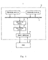
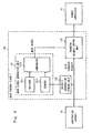
- Fig. 1 is a block diagram showing a configuration example of a processor system according to a first embodiment.
- the processor system according to the first embodiment includes a mask control circuit that sequentially outputs a plurality of data transfer requests, which are output from an arbitration circuit, to a memory controller after a lapse of a mask period.
- This allows the processor system according to the first embodiment (and the semiconductor device provided therein) to effectively set a mode of a memory to a power saving mode, thereby suppressing an increase in power consumption.
- This processor system (and the semiconductor device provided therein) is applied to, for example, a radio communication terminal such as a cellular phone.
- the processor system will be described in detail below.
- a processor system 1 shown in Fig. 1 includes a semiconductor device 10 and a DRAM 20. Note that a memory such as an SRAM or an FRAM (Registered Trademark) may be used instead of the DRAM 20.
- the semiconductor device 10 is a semiconductor chip, and includes at least n (n is an integer equal to or greater than 2) processing blocks (processing circuits) B1 to Bn, a bus 11, an arbitration circuit 12, a mask control circuit 13, and a memory controller 14.
- the processing blocks B1 to Bn are, for example, arithmetic processing circuits such as CPUs, or data processing circuits such as graphics engines.
- the processing blocks B1 to Bn issue data transfer requests RQ1 to RQn, respectively, to the DRAM 20 at a given timing. These data transfer requests RQ1 to RQn are supplied to the mask control circuit 13 via the bus 11 and the arbitration circuit 12.
- the arbitration circuit 12 determines the order of priority of a plurality of data transfer requests in accordance with a predetermined rule (for example, when a plurality of data transfer requests are simultaneously issued), and sequentially outputs the data transfer requests one by one to the mask control circuit 13.
- the mask control circuit 13 loads the plurality of data transfer requests output from the arbitration circuit 12, and sequentially outputs, to the memory controller 14, the plurality of loaded data transfer requests after the lapse of the mask period.
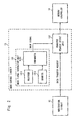
- Fig. 2 is a block diagram showing a specific configuration example of the mask control circuit 13.
- the mask control circuit 13 shown in Fig. 2 includes a mask signal generation unit 131 and a transfer request output unit 132.
- the mask signal generation unit 131 includes a register 1311, a counter 1312, and a comparator 1313.
- the mask signal generation unit 131 generates a mask signal that is periodically switched between an active state and an inactive state.
- the counter 1312 increases the count value by "1" in synchronization with a clock signal.
- the count value reaches a maximum value MAX
- the counter 1312 resets the count value to "0".
- the register 1311 stores a predetermined threshold Nt.
- the comparator 1313 compares the count value of the counter 1312 with the threshold Nt.
- the comparator 1313 sets the mask signal to the active state (for example, H level), and when the count value of the counter 1312 is larger than the threshold Nt, the comparator 1313 sets the mask signal to the inactive state (for example, L level).
- a period in which the mask signal is in the active state is referred to as a mask period, and a period in which the mask signal is in the inactive state is referred to as a mask release period.
- the transfer request output unit 132 loads the plurality of data transfer requests, which are sequentially output from the arbitration circuit 12, and sequentially outputs the plurality of loaded data transfer requests when the mask signal is in the inactive state (during the mask release period).
- the transfer request output unit 132 includes at least a configuration (so-called FIFO) that first outputs a data transfer request that is first input.
- the memory controller 14 accesses the DRAM 20 based on the data transfer requests sequentially output from the mask control circuit 13. For example, the memory controller 14 reads out data stored in a memory cell at a designated address in the DRAM 20, or writes data into a memory cell at a designated address in the DRAM 20, based on the data transfer requests. The memory controller 14 outputs data read from the DRAM 20, or information on data write completion notification indicating completion of data write to the DRAM 20, to the processing blocks which have issued the data transfer requests, via the bus 11.
- the memory controller 14 When a subsequent data transfer request is not present (not received) for a predetermined period after completion of access to the DRAM 20 based on a certain data transfer request, the memory controller 14 causes the mode of the DRAM 20 to be switched from a normal operation mode to a power saving mode, and maintains the power saving mode until the subsequent data transfer request is received.
- the term "power saving mode" of the DRAM 20 refers to a so-called self-refresh mode.
- the DRAM 20 repeatedly executes a refresh operation autonomously by a timer which is incorporated therein or connected thereto. At this time, the DRAM 20 is only supplied with power, while it is not supplied with any clock signal. This results in a reduction in power consumption of the DRAM 20.
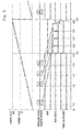
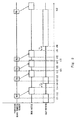
- FIG. 3 is a timing diagram showing an operation of the processor system 1 according to the first embodiment.
- the counter 1312 starts a count-up operation from the count value "0" which is the initial value.
- the mask signal becomes active, and the mode of the DRAM 20 is set to the power saving mode.
- the processing block B1 issues the first data transfer request RQ1 (time t11).
- the processing block Bn sequentially issues the first data transfer request RQn and the second data transfer request RQn, and then the processing block B1 issues the second data transfer request RQ1 (times t12, t13, t14).
- the count value of the counter 1312 is equal to or less than the threshold Nt, so the mask signal is maintained in the active state. Accordingly, the mask control circuit 13 does not output the data transfer request to the memory controller 14 (from time t11 to time t15).
- the memory controller 14 maintains the power saving mode of the DRAM 20 without causing the mode to be switched to the normal operation mode (from time t11 to time t21).
- the mask control circuit 13 sequentially outputs the plurality of loaded data transfer requests (four data transfer requests in the example shown in Fig. 3 ) to the memory controller 14.
- the memory controller 14 accesses the DRAM 20 based on the plurality of data transfer requests sequentially output from the mask control circuit 13 (times t21, t22, t23, t24).
- the memory controller 14 Upon receiving the data transfer requests, the memory controller 14 causes the mode of the DRAM 20 to be switched from the power saving mode to the normal operation mode (time t21) .
- the mask control circuit 13 stops the output of data transfer requests to the memory controller 14. Since the memory controller 14 has not received a subsequent data transfer request during the predetermined period T1 after the completion of the access to the DRAM 20, the memory controller 14 causes the mode of the DRAM 20 to be switched from the normal operation mode to the power saving mode (time t25). The operation described above is then repeated.
- the threshold Nt and the maximum value MAX of the count value can be arbitrarily set. In other words, the length of each of the mask period and the mask release period, which are periodically switched, can be arbitrarily set. However, it is necessary to set the threshold Nt and the maximum value MAX of the count value so as to satisfy all the required performances of the plurality of processing blocks B1 to Bn, respectively.
- the term "required performance" of a certain processing block refers to a time period required from when a certain processing block issues a data transfer request until when the processing block receives data (or data write completion notification) read from the DRAM 20.
- the mask control circuit 13 When the mask control circuit 13 cannot output all the loaded data transfer requests during the mask release period, the mask control circuit 13 outputs the remaining data transfer requests, which have not been output, during the subsequent mask release period.
- the processor system 1 according to the first embodiment includes the control circuit 13 that sequentially outputs the plurality of data transfer requests, which are output from the arbitration circuit 12, to the memory controller 14 after the lapse of the mask period.
- This allows the processor system 1 according to the first embodiment (and the semiconductor device 10 provided therein) to effectively set the mode of the DRAM 20 to the power saving mode, thereby suppressing an increase in power consumption.
- the processor system 1a according to the second embodiment includes a mask control circuit 13a in place of the mask control circuit 13.
- the other components of the processor system 1a are similar to those of the processor system 1, so the description thereof is omitted.
- the mask control circuit 13a dynamically sets the mask period based on the total amount of data on the data transfer requests issued from the plurality of processing blocks B1 to Bn during the monitoring period. For example, when the total amount of data on the data transfer requests issued from the plurality of processing blocks B1 to Bn during the monitoring period is large, the mask control circuit 13a determines that access to the DRAM 20 is concentrated, and decreases the mask period. When the total amount of data on the data transfer requests issued from the plurality of processing blocks B1 to Bn during the monitoring period is small, the mask control circuit 13a determines that the DRAM 20 is less frequently accessed, and increases the mask period.
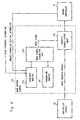
- Fig. 4 is a block diagram showing a specific configuration of the mask control circuit 13a.
- the mask control circuit 13a shown in Fig. 4 includes a mask signal generation unit 131a, the transfer request output unit 132, a DRAM band monitor (first monitor) 133, and a transaction monitor (second monitor) 134.
- the DRAM band monitor 133 calculates the total amount of data that can be accepted by the DRAM 20, based on clock frequency information, memory controller setting information, or the like.
- the transaction monitor 134 measures the total amount of data (the number of bytes) on data transfer requests issued during a certain monitoring period.
- the mask signal generation unit 131a calculates the remaining amount of data that can be accepted by the DRAM 20 during a certain monitoring period, based on a monitoring result of the DRAM band monitor 133 and a monitoring result of the transaction monitor 134. Further, the mask signal generation unit 131a sets, as a mask period in a subsequent monitoring period, a period corresponding to the remaining amount of data that can be accepted by the DRAM 20.
- the mask signal generation unit 131a determines that access to the DRAM 20 is concentrated, and decreases the mask period in the subsequent monitoring period.
- the mask signal generation unit 131a determines that the DRAM 20 is less frequently accessed, and increases the mask period in the subsequent monitoring period.
- FIG. 5 is a timing diagram showing an operation of the processor system 1a according to the second embodiment.
- 11 data transfer requests are issued.
- the total amount of data on the 11 data transfer requests corresponds to 80% of the total amount of data that can be accepted by the DRAM 20.
- the remaining amount of data that can be accepted by the DRAM 20 corresponds to 20% of the total amount of data. That is, the DRAM 20 is relatively frequently accessed during the monitoring period P1. Accordingly, a relatively short mask period is set in a subsequent monitoring period P2.
- the total amount of data on the six data transfer requests corresponds to 40% of the total amount of data that can be accepted by the DRAM 20.
- the remaining amount of data that can be accepted by the DRAM 20 corresponds to 60% of the total amount of data. That is, the DRAM 20 is less frequently accessed in the monitoring period P2 than in the monitoring period P1. Accordingly, a relatively long mask period is set in a subsequent monitoring period P3.
- the total amount of data on the three data transfer requests corresponds to 20% of the total amount of data that can be accepted by the DRAM 20.
- the remaining amount of data that can be accepted by the DRAM 20 corresponds to 80% of the total amount of data. That is, the DRAM 20 is much less frequently accessed in the monitoring period P3 than in the monitoring period P2. Accordingly, a much longer mask period is set in a subsequent monitoring period.
- the processor system 1a according to the second embodiment includes the mask control circuit 13a that dynamically sets the mask period based on the total amount of data on the data transfer requests issued from the plurality of processing blocks B1 to Bn during the monitoring period.
- the processor system 1a according to the second embodiment and the semiconductor device provided therein) to effectively set the mode of the DRAM 20 to the power saving mode, thereby further suppressing an increase in power consumption.
- the second embodiment illustrates a case where a mask period in a subsequent monitoring period is set based on the total amount of data on the data transfer requests issued during a certain monitoring period
- the present invention is not limited to this.
- the mask period in the subsequent monitoring period may be set based on an average value of the total amounts of data on data transfer requests issued in a plurality of monitoring periods.
- the processor system 1b according to the third embodiment includes a mask control circuit 13b in place of the mask control circuit 13.
- the processing blocks B1 to Bn output the data transfer requests RQ1 to RQn, respectively, and also output QoS (Quality of Service) information (hereinafter referred to as "priority information") PR1 to PRn, respectively, which indicate priorities of the data transfer requests.
- QoS Quality of Service
- PR1 to PRn QoS (Quality of Service) information
- the mask control circuit 13b outputs, to the memory controller 14, each data transfer request output from the arbitration circuit 12, after a lapse of a mask period of a length that is set according to the priority of each data transfer request. For example, when the priority of a certain data transfer request is high, the mask control circuit 13b decreases the mask period, and when the priority of a certain data transfer request is low, the mask control circuit 13b increases the mask period.
- Fig. 6 is a block diagram showing a specific configuration example of the mask control circuit 13b.
- the mask control circuit 13b shown in Fig. 6 includes the mask signal generation unit 131, the transfer request output unit 132, and a priority information storage unit 135.
- the priority information storage unit 135 stores the priority information corresponding to the data transfer requests output from the arbitration circuit 12.
- the priority information storage unit 135 includes at least a configuration (so-called FIFO) that first outputs a data transfer request that is first input.
- the counter 1312 provided in the mask signal generation unit 131 starts a count-up operation from a count value set based on the priority information stored in the priority information storage unit 135.
- the counter 1312 starts the count-up operation from a high count value
- the counter 1312 starts the count-up operation from a low count value. Accordingly, when the priority is high, the active period (mask period) of the mask signal is short, and when the priority is low, the active period (mask period) of the mask signal is long.
- FIG. 7 is a timing diagram showing an operation of the processor system 1b according to the third embodiment.
- the count value of the counter 1312 is reset to "0", and the mode of the DRAM 20 is set to the power saving mode.
- the processing block B1 issues the first data transfer request RQ1 and priority information on the first data transfer request RQ1 (time t11).
- the priority of the data transfer request RQ1 is low, so the count value is set to "1".
- the counter 1312 starts the count-up operation from the count value "1" (time t11).
- the mask signal becomes active.
- the mask control circuit 13b does not output any data transfer request RQ to the memory controller 14 (from time t11 to time t12) .
- the mask signal is switched from the active state to the inactive state (time t12). Accordingly, the mask control circuit 13b outputs the loaded data transfer request RQ1 to the memory controller 14.
- the memory controller 14 accesses the DRAM 20 based on the data transfer request RQ1 output from the mask control circuit 13b (time t13).
- the memory controller 14 Upon receiving the data transfer request RQ1, the memory controller 14 causes the mode of the DRAM 20 to be switched from the power saving mode to the normal operation mode (time t13) .
- the processing block Bn issues the first data transfer request RQn and priority information on the first data transfer request RQn (time t21).
- the priority of the data transfer request RQn is low, so the count value is set to "1".
- the operation proceeds in the same way as that during the period from time t11 to time t13 (from time t21 to time t23).
- the processing block Bn issues the second data transfer request RQn and priority information on the second data transfer request RQn (time t31).
- the mask control circuit 13b rapidly outputs the loaded data transfer request RQ1 to the memory controller 14 without masking the data transfer request.
- the memory controller 14 accesses the DRAM 20 based on the data transfer request RQn output from the mask control circuit 13b (time t33).
- the processing block B1 issues the second data transfer request RQ1 and priority information on the second data transfer request RQ1 (time t41).
- the priority of the data transfer request RQ1 is low, so the count value is set to "1".
- the operation proceeds in the same way as that during the period from time t11 to time t13 (time t41 to t43).
- the processor system 1b according to the third embodiment includes the mask control circuit 13b that outputs, to the memory controller 14, each data transfer request output from the arbitration circuit 12, after a lapse of a mask period of a length that is set according to the priority of each data transfer request.
- This allows the processor system 1b according to the third embodiment (and the semiconductor device provided therein) to effectively set the mode of the DRAM 20 to the power saving mode, thereby suppressing an increase in power consumption.
- the processor systems according to the first to third embodiments and semiconductor devices provided therein include the mask control circuit that compresses a plurality of data transfer requests sequentially output from the arbitration circuit, and sequentially outputs the data transfer requests to the memory controller after a lapse of a mask period. This allows the processor systems according to the embodiments to effectively set the mode of the memory to the power saving mode, thereby suppressing an increase in power consumption.
- the configuration of the mask control circuit is not disclosed in any of Japanese Unexamined Patent Application Publication Nos. 2012-133638 , 2004-120781 , 2007-257774 , and 2007-94649 . Therefore, it is difficult for the configurations disclosed in this related art to sufficiently suppress an increase in power consumption. On the other hand, such a problem does not occur in the processor systems according to the embodiments described above and semiconductor devices provided therein.
- the memory circuit outputs the control signal WAIT to the control circuit during a read transfer or a write transfer, thereby limiting access from the control circuit, but is not intended to suppress an increase in power consumption. Additionally, the mode of the memory circuit is not switched to the power saving mode.
- the configuration disclosed in Japanese Unexamined Patent Application Publication No. 2007-257774 adjusts a timing for refreshing a DRAM according to the degree of congestion of a bus used for a data transfer with the DRAM, but is not intended to suppress an increase in power consumption. Additionally, the mode of the DRAM is not switched to the power saving mode.
- the configuration disclosed in Japanese Unexamined Patent Application Publication No. 2007-94649 dynamically changes the order of priority of previously stored access requests based on the order of priority of newly stored access requests. Additionally, the mode of the memory is not switched to the power saving mode.
- the first to third embodiments can be combined as desirable by one of ordinary skill in the art.
Landscapes
- Engineering & Computer Science (AREA)
- Theoretical Computer Science (AREA)
- Physics & Mathematics (AREA)
- General Engineering & Computer Science (AREA)
- General Physics & Mathematics (AREA)
- Human Computer Interaction (AREA)
- Dram (AREA)
- Memory System (AREA)
- Multi Processors (AREA)
Abstract
Description
- The present invention relates to a semiconductor device and a processor system including the semiconductor device. More particularly, the present invention relates to a semiconductor device suitable for suppressing an increase in power consumption, and a processor system including the semiconductor device.
- In the fields of a baseband processor and an application processor for cellular phones, the respective requirements regarding the function and performance thereof have become exacting. To satisfy such requirements, the capacity of a memory, such as a DRAM, has been increased, or the operating frequency of a processor has been increased, which results in a problem of an increase in power consumption.
- For example, Japanese Unexamined Patent Application Publication No.
2012-133638 - Additionally, Japanese Unexamined Patent Application Publication No.
2004-120781 - Japanese Unexamined Patent Application Publication No.
2007-257774 - Japanese Unexamined Patent Application Publication No.
2007-94649 - The present inventors have found various problems in the process of developing a semiconductor device and a processor system including the semiconductor device. Each embodiment disclosed herein provides a semiconductor device suitable for a radio communication terminal, such as a cellular phone, and a processor system including the semiconductor device. Further detailed features will be apparent from the following description and the accompanying drawings.
- According to one aspect of the present invention, a mask control circuit is provided that loads a plurality of data transfer requests arbitrated by an arbitration circuit, and sequentially outputs the plurality of data transfer requests after a lapse of a mask period.
- According to one aspect of the present invention, it is possible to provide a high-quality semiconductor device and a processor system including the semiconductor device.
- The above and other aspects, advantages and features will be more apparent from the following description of certain embodiments taken in conjunction with the accompanying drawings, in which:
-
Fig. 1 is a block diagram showing a configuration example of a processor system according to a first embodiment; -
Fig. 2 is a block diagram showing a configuration example of a mask control circuit according to the first embodiment; -
Fig. 3 is a timing diagram showing an operation of a processor system according to the first embodiment; -
Fig. 4 is a block diagram showing a configuration example of a mask control circuit according to a second embodiment; -
Fig. 5 is a timing diagram showing an operation of a processor system according to the second embodiment; -
Fig. 6 is a block diagram showing a configuration example of a mask control circuit according to a third embodiment; -
Fig. 7 is a timing diagram showing an operation of a processor system according to the third embodiment; -
Fig. 8 is a block diagram showing a configuration example of a processor system reviewed by the present inventors; and -
Fig. 9 is a timing diagram showing an operation of the processor system reviewed by the present inventors. - Details of the preliminary review by the present inventors will be described prior to the description of embodiments.
-
Fig. 8 is a block diagram showing a configuration example of aprocessor system 50 according to an idea conceived of before an embodiment of the invention was accomplished. Theprocessor system 50 shown inFig. 8 includes asemiconductor device 500 and aDRAM 600. - The
semiconductor device 500 includes at least n (n is an integer equal to or greater than 2) processing blocks B1 to Bn, abus 501, anarbitration circuit 502, and amemory controller 504. - The processing blocks B1 to Bn are, for example, arithmetic processing circuits such as CPUs, or data processing circuits such as graphics engines. The processing blocks B1 to Bn issue data transfer requests RQ1 to RQn, respectively, to the
DRAM 600 at a given timing. The data transfer requests RQ1 to RQn are supplied to thememory controller 504 via thebus 501 and thearbitration circuit 502. In this case, thearbitration circuit 502 determines the order of priority of a plurality of data transfer requests in accordance with a predetermined rule (for example, when a plurality of data transfer requests are simultaneously issued), and sequentially outputs the data transfer requests one by one to thememory controller 504. - The
memory controller 504 accesses theDRAM 600 based on the data transfer requests sequentially output from thearbitration circuit 502. For example, thememory controller 504 reads out data stored in a memory cell at a designated address in theDRAM 600 based on the data transfer request, or writes data into a memory cell at a designated address in theDRAM 600, based on the data transfer requests. Thememory controller 504 outputs data read from theDRAM 600, or information on data write completion notification indicating completion of data write to theDRAM 600, to the processing blocks which have issued the data transfer requests, via thebus 501. - When a subsequent data transfer request is not present (not received) for a predetermined period after completion of access to the
DRAM 600 based on a certain data transfer request, thememory controller 504 causes the mode of theDRAM 600 to be switched from a normal operation mode to a power saving mode, and maintains the power saving mode until the subsequent data transfer request is received. - The term "power saving mode" of the
DRAM 600 refers to a so-called self-refresh mode. In the self-refresh mode, theDRAM 600 repeatedly executes a refresh operation autonomously by a timer which is incorporated therein or connected thereto. At this time, theDRAM 600 is only supplied with power, while it is not supplied with any clock signal. This results in a reduction in power consumption of theDRAM 600. - Referring next to
Fig. 9 , an operation of theprocessor system 50 shown inFig. 8 will be described.Fig. 9 is a timing diagram showing an operation of theprocessor system 50. - First, the processing block B1 issues the first data transfer request RQ1 (time t11). Upon receiving the data transfer request RQ1, the
memory controller 504 accesses theDRAM 600 based on the data transfer request RQ1 (from time t12 to time t13). Since thememory controller 504 receives no subsequent data transfer request for a predetermined period T1 after the completion of the access to theDRAM 600, thememory controller 504 causes the mode of theDRAM 600 to be switched from the normal operation mode to the power saving mode (time t14) . - Next, the processing block Bn issues the first data transfer request RQn (time t21). Upon receiving the data transfer request RQn, the
memory controller 504 accesses theDRAM 600 based on the data transfer request RQn (from time t22 to time t23). Upon receiving the data transfer request RQn, thememory controller 504 causes the mode of theDRAM 600 to be switched from the power saving mode to the normal operation mode (time t22). Since thememory controller 504 receives the subsequent data transfer request during the period from the completion of the access to theDRAM 600 to the lapse of the predetermined period T1, thememory controller 504 maintains the normal operation mode of theDRAM 600 without causing the mode to be switched to the power saving mode. - Next, the processing block Bn issues the second data transfer request RQn (time t31). Upon receiving the data transfer request RQn, the
memory controller 504 accesses theDRAM 600 based on the data transfer request RQn (from time t32 to time t33). Since thememory controller 504 receives the subsequent data transfer request during the period from the completion of the access to theDRAM 600 to the lapse of the predetermined period T1, thememory controller 504 maintains the normal operation mode of theDRAM 600 without causing the mode to be switched to the power saving mode. - Next, the processing block B1 issues the second data transfer request RQ1 (time t41). Upon receiving the data transfer request RQ1, the
memory controller 504 accesses theDRAM 600 based on the data transfer request RQ1 (from time t42 to time t43). Since thememory controller 504 receives no subsequent data transfer request during the period from the completion of the access to theDRAM 600 to the lapse of the predetermined period T1, thememory controller 504 causes the mode of theDRAM 600 to be switched from the normal operation mode to the power saving mode (time t44). Then thememory controller 504 maintains the power saving mode until the subsequent data transfer request is received (RQn) (from time t44 to time t52). - In the
processor system 50 shown inFig. 8 , the period in which the mode ofDRAM 600 is set to the power saving mode is shortened depending on the interval or frequency of access to theDRAM 600. For example, when the subsequent data transfer request is received after the completion of the access to theDRAM 600 and immediately before the lapse of the predetermined period T1, the mode of theDRAM 600 is maintained as the normal operation mode. When the access to theDRAM 600 is repeated at such intervals, the period in which the mode of theDRAM 600 is set to the power saving mode is shortened. Thus, theprocessor system 50 shown inFig. 8 has a problem that it is difficult to sufficiently suppress an increase in power consumption. - Hereinafter, embodiments will be described with reference to the drawings. The drawings are made in a simplified manner, and therefore the technical scope of embodiments should not be narrowly interpreted based on the drawings. The same components are denoted by the same reference numerals, so repeated description thereof is omitted.
- In the following embodiments, explanations are made by referring to several sections or several embodiments for convenience, as required, but they are mutually related, and are in such a relation to each other that one of them is a modified example, an application example, a detailed explanation, a supplemental explanation, or the like of a part or all of the other, unless otherwise specified. Further, in the following embodiments, when a number of an element (including number, numerical value, quantity, range etc.) or the like is mentioned, the number is not limited to that specific number, and may be larger or smaller than the mentioned number, except for the case where it is explicitly indicated that the number should be the specifically-mentioned number, or it is theoretically clear that the number should be limited to the specifically-mentioned number.
- Further, in the following embodiments, the constituent elements thereof (including operation steps etc.) are not necessarily indispensable, except for the case where it is explicitly indicated that a specific element is indispensable, or it is theoretically clear that a specific element is indispensable. Similarly, in the following embodiments, when shapes, positional relationship etc. of the constituent elements are mentioned, they include substantially similar or analogous shapes and so forth, except for the case where it is explicitly indicated, or it is theoretically clear that the above is not true. This also applies to the above-mentioned values (including number, numerical value, quantity, range, etc.) and the like.
-
Fig. 1 is a block diagram showing a configuration example of a processor system according to a first embodiment. The processor system according to the first embodiment (and a semiconductor device provided therein) includes a mask control circuit that sequentially outputs a plurality of data transfer requests, which are output from an arbitration circuit, to a memory controller after a lapse of a mask period. This allows the processor system according to the first embodiment (and the semiconductor device provided therein) to effectively set a mode of a memory to a power saving mode, thereby suppressing an increase in power consumption. This processor system (and the semiconductor device provided therein) is applied to, for example, a radio communication terminal such as a cellular phone. The processor system will be described in detail below. - A
processor system 1 shown inFig. 1 includes asemiconductor device 10 and aDRAM 20. Note that a memory such as an SRAM or an FRAM (Registered Trademark) may be used instead of theDRAM 20. Thesemiconductor device 10 is a semiconductor chip, and includes at least n (n is an integer equal to or greater than 2) processing blocks (processing circuits) B1 to Bn, abus 11, anarbitration circuit 12, amask control circuit 13, and amemory controller 14. - The processing blocks B1 to Bn are, for example, arithmetic processing circuits such as CPUs, or data processing circuits such as graphics engines. The processing blocks B1 to Bn issue data transfer requests RQ1 to RQn, respectively, to the
DRAM 20 at a given timing. These data transfer requests RQ1 to RQn are supplied to themask control circuit 13 via thebus 11 and thearbitration circuit 12. In this case, thearbitration circuit 12 determines the order of priority of a plurality of data transfer requests in accordance with a predetermined rule (for example, when a plurality of data transfer requests are simultaneously issued), and sequentially outputs the data transfer requests one by one to themask control circuit 13. - The
mask control circuit 13 loads the plurality of data transfer requests output from thearbitration circuit 12, and sequentially outputs, to thememory controller 14, the plurality of loaded data transfer requests after the lapse of the mask period. -
Fig. 2 is a block diagram showing a specific configuration example of themask control circuit 13. Themask control circuit 13 shown inFig. 2 includes a masksignal generation unit 131 and a transferrequest output unit 132. The masksignal generation unit 131 includes aregister 1311, acounter 1312, and acomparator 1313. - The mask
signal generation unit 131 generates a mask signal that is periodically switched between an active state and an inactive state. In the masksignal generation unit 131, thecounter 1312 increases the count value by "1" in synchronization with a clock signal. When the count value reaches a maximum value MAX, thecounter 1312 resets the count value to "0". Theregister 1311 stores a predetermined threshold Nt. Thecomparator 1313 compares the count value of thecounter 1312 with the threshold Nt. Specifically, when the count value of thecounter 1312 is equal to or less than the threshold Nt, thecomparator 1313 sets the mask signal to the active state (for example, H level), and when the count value of thecounter 1312 is larger than the threshold Nt, thecomparator 1313 sets the mask signal to the inactive state (for example, L level). A period in which the mask signal is in the active state is referred to as a mask period, and a period in which the mask signal is in the inactive state is referred to as a mask release period. - The transfer
request output unit 132 loads the plurality of data transfer requests, which are sequentially output from thearbitration circuit 12, and sequentially outputs the plurality of loaded data transfer requests when the mask signal is in the inactive state (during the mask release period). The transferrequest output unit 132 includes at least a configuration (so-called FIFO) that first outputs a data transfer request that is first input. - Returning to
Fig. 1 , thememory controller 14 accesses theDRAM 20 based on the data transfer requests sequentially output from themask control circuit 13. For example, thememory controller 14 reads out data stored in a memory cell at a designated address in theDRAM 20, or writes data into a memory cell at a designated address in theDRAM 20, based on the data transfer requests. Thememory controller 14 outputs data read from theDRAM 20, or information on data write completion notification indicating completion of data write to theDRAM 20, to the processing blocks which have issued the data transfer requests, via thebus 11. - When a subsequent data transfer request is not present (not received) for a predetermined period after completion of access to the
DRAM 20 based on a certain data transfer request, thememory controller 14 causes the mode of theDRAM 20 to be switched from a normal operation mode to a power saving mode, and maintains the power saving mode until the subsequent data transfer request is received. - The term "power saving mode" of the
DRAM 20 refers to a so-called self-refresh mode. In the self-refresh mode, theDRAM 20 repeatedly executes a refresh operation autonomously by a timer which is incorporated therein or connected thereto. At this time, theDRAM 20 is only supplied with power, while it is not supplied with any clock signal. This results in a reduction in power consumption of theDRAM 20. - Referring next to
Fig. 3 , an operation of theprocessor system 1 according to the first embodiment will be described.Fig. 3 is a timing diagram showing an operation of theprocessor system 1 according to the first embodiment. - In an initial state (time t0), the
counter 1312 starts a count-up operation from the count value "0" which is the initial value. At the same time, the mask signal becomes active, and the mode of theDRAM 20 is set to the power saving mode. - First, the processing block B1 issues the first data transfer request RQ1 (time t11). After that, the processing block Bn sequentially issues the first data transfer request RQn and the second data transfer request RQn, and then the processing block B1 issues the second data transfer request RQ1 (times t12, t13, t14). During this period, the count value of the
counter 1312 is equal to or less than the threshold Nt, so the mask signal is maintained in the active state. Accordingly, themask control circuit 13 does not output the data transfer request to the memory controller 14 (from time t11 to time t15). Thus, thememory controller 14 maintains the power saving mode of theDRAM 20 without causing the mode to be switched to the normal operation mode (from time t11 to time t21). - After that, when the count value of the
counter 1312 is larger than the threshold Nt, the mask signal is switched from the active state to the inactive state (time t15). Accordingly, themask control circuit 13 sequentially outputs the plurality of loaded data transfer requests (four data transfer requests in the example shown inFig. 3 ) to thememory controller 14. Thememory controller 14 accesses theDRAM 20 based on the plurality of data transfer requests sequentially output from the mask control circuit 13 (times t21, t22, t23, t24). Upon receiving the data transfer requests, thememory controller 14 causes the mode of theDRAM 20 to be switched from the power saving mode to the normal operation mode (time t21) . - After that, when the count value of the
counter 1312 reaches the maximum value MAX, the count value of thecounter 1312 is reset to "0", so the mask signal is switched from the inactive state to the active state (time t26). Accordingly, themask control circuit 13 stops the output of data transfer requests to thememory controller 14. Since thememory controller 14 has not received a subsequent data transfer request during the predetermined period T1 after the completion of the access to theDRAM 20, thememory controller 14 causes the mode of theDRAM 20 to be switched from the normal operation mode to the power saving mode (time t25). The operation described above is then repeated. - The threshold Nt and the maximum value MAX of the count value can be arbitrarily set. In other words, the length of each of the mask period and the mask release period, which are periodically switched, can be arbitrarily set. However, it is necessary to set the threshold Nt and the maximum value MAX of the count value so as to satisfy all the required performances of the plurality of processing blocks B1 to Bn, respectively. The term "required performance" of a certain processing block refers to a time period required from when a certain processing block issues a data transfer request until when the processing block receives data (or data write completion notification) read from the
DRAM 20. - When the
mask control circuit 13 cannot output all the loaded data transfer requests during the mask release period, themask control circuit 13 outputs the remaining data transfer requests, which have not been output, during the subsequent mask release period. - In this manner, the
processor system 1 according to the first embodiment (and thesemiconductor device 10 provided therein) includes thecontrol circuit 13 that sequentially outputs the plurality of data transfer requests, which are output from thearbitration circuit 12, to thememory controller 14 after the lapse of the mask period. This allows theprocessor system 1 according to the first embodiment (and thesemiconductor device 10 provided therein) to effectively set the mode of theDRAM 20 to the power saving mode, thereby suppressing an increase in power consumption. - Next, a processor system 1a according to a second embodiment will be described. As compared with the
processor system 1 according to the first embodiment, the processor system 1a according to the second embodiment includes amask control circuit 13a in place of themask control circuit 13. The other components of the processor system 1a are similar to those of theprocessor system 1, so the description thereof is omitted. - The
mask control circuit 13a dynamically sets the mask period based on the total amount of data on the data transfer requests issued from the plurality of processing blocks B1 to Bn during the monitoring period. For example, when the total amount of data on the data transfer requests issued from the plurality of processing blocks B1 to Bn during the monitoring period is large, themask control circuit 13a determines that access to theDRAM 20 is concentrated, and decreases the mask period. When the total amount of data on the data transfer requests issued from the plurality of processing blocks B1 to Bn during the monitoring period is small, themask control circuit 13a determines that theDRAM 20 is less frequently accessed, and increases the mask period. -
Fig. 4 is a block diagram showing a specific configuration of themask control circuit 13a. Themask control circuit 13a shown inFig. 4 includes a masksignal generation unit 131a, the transferrequest output unit 132, a DRAM band monitor (first monitor) 133, and a transaction monitor (second monitor) 134. - The DRAM band monitor 133 calculates the total amount of data that can be accepted by the
DRAM 20, based on clock frequency information, memory controller setting information, or the like. - The transaction monitor 134 measures the total amount of data (the number of bytes) on data transfer requests issued during a certain monitoring period.
- The mask
signal generation unit 131a calculates the remaining amount of data that can be accepted by theDRAM 20 during a certain monitoring period, based on a monitoring result of the DRAM band monitor 133 and a monitoring result of thetransaction monitor 134. Further, the masksignal generation unit 131a sets, as a mask period in a subsequent monitoring period, a period corresponding to the remaining amount of data that can be accepted by theDRAM 20. - For example, when the remaining amount of data that can be accepted by the
DRAM 20 during a certain monitoring period is small, the masksignal generation unit 131a determines that access to theDRAM 20 is concentrated, and decreases the mask period in the subsequent monitoring period. When the remaining amount of data that can be accepted by theDRAM 20 during a certain monitoring period is large, the masksignal generation unit 131a determines that theDRAM 20 is less frequently accessed, and increases the mask period in the subsequent monitoring period. - Referring next to
Fig. 5 , an operation of the processor system 1a according to the second embodiment will be described.Fig. 5 is a timing diagram showing an operation of the processor system 1a according to the second embodiment. - First, during a monitoring period P1, 11 data transfer requests are issued. In the example shown in
Fig. 5 , the total amount of data on the 11 data transfer requests corresponds to 80% of the total amount of data that can be accepted by theDRAM 20. In other words, the remaining amount of data that can be accepted by theDRAM 20 corresponds to 20% of the total amount of data. That is, theDRAM 20 is relatively frequently accessed during the monitoring period P1. Accordingly, a relatively short mask period is set in a subsequent monitoring period P2. - Next, in the monitoring period P2, six data transfer requests are issued. In the example shown in
Fig. 5 , the total amount of data on the six data transfer requests corresponds to 40% of the total amount of data that can be accepted by theDRAM 20. In other words, the remaining amount of data that can be accepted by theDRAM 20 corresponds to 60% of the total amount of data. That is, theDRAM 20 is less frequently accessed in the monitoring period P2 than in the monitoring period P1. Accordingly, a relatively long mask period is set in a subsequent monitoring period P3. - Next, in the monitoring period P3, three data transfer requests are issued. In the example shown in
Fig. 5 , the total amount of data on the three data transfer requests corresponds to 20% of the total amount of data that can be accepted by theDRAM 20. In other words, the remaining amount of data that can be accepted by theDRAM 20 corresponds to 80% of the total amount of data. That is, theDRAM 20 is much less frequently accessed in the monitoring period P3 than in the monitoring period P2. Accordingly, a much longer mask period is set in a subsequent monitoring period. - In this manner, the processor system 1a according to the second embodiment (and a semiconductor device provided therein) includes the
mask control circuit 13a that dynamically sets the mask period based on the total amount of data on the data transfer requests issued from the plurality of processing blocks B1 to Bn during the monitoring period. This allows the processor system 1a according to the second embodiment (and the semiconductor device provided therein) to effectively set the mode of theDRAM 20 to the power saving mode, thereby further suppressing an increase in power consumption. - Though the second embodiment illustrates a case where a mask period in a subsequent monitoring period is set based on the total amount of data on the data transfer requests issued during a certain monitoring period, the present invention is not limited to this. The mask period in the subsequent monitoring period may be set based on an average value of the total amounts of data on data transfer requests issued in a plurality of monitoring periods.
- Next, a processor system 1b according to third embodiment will be described. As compared with the
processor system 1 according to the first embodiment, the processor system 1b according to the third embodiment includes amask control circuit 13b in place of themask control circuit 13. The processing blocks B1 to Bn output the data transfer requests RQ1 to RQn, respectively, and also output QoS (Quality of Service) information (hereinafter referred to as "priority information") PR1 to PRn, respectively, which indicate priorities of the data transfer requests. The other components of the processor system 1b are similar to those of theprocessor system 1, so the description thereof is omitted. - The
mask control circuit 13b outputs, to thememory controller 14, each data transfer request output from thearbitration circuit 12, after a lapse of a mask period of a length that is set according to the priority of each data transfer request. For example, when the priority of a certain data transfer request is high, themask control circuit 13b decreases the mask period, and when the priority of a certain data transfer request is low, themask control circuit 13b increases the mask period. -
Fig. 6 is a block diagram showing a specific configuration example of themask control circuit 13b. Themask control circuit 13b shown inFig. 6 includes the masksignal generation unit 131, the transferrequest output unit 132, and a priorityinformation storage unit 135. - The priority
information storage unit 135 stores the priority information corresponding to the data transfer requests output from thearbitration circuit 12. The priorityinformation storage unit 135 includes at least a configuration (so-called FIFO) that first outputs a data transfer request that is first input. - The
counter 1312 provided in the masksignal generation unit 131 starts a count-up operation from a count value set based on the priority information stored in the priorityinformation storage unit 135. - For example, when the priority is high, the
counter 1312 starts the count-up operation from a high count value, and when the priority is low, thecounter 1312 starts the count-up operation from a low count value. Accordingly, when the priority is high, the active period (mask period) of the mask signal is short, and when the priority is low, the active period (mask period) of the mask signal is long. - Referring next to
Fig. 7 , an operation of the processor system 1b according to the third embodiment will be described.Fig. 7 is a timing diagram showing an operation of the processor system 1b according to the third embodiment. - In an initial state (time t0), the count value of the
counter 1312 is reset to "0", and the mode of theDRAM 20 is set to the power saving mode. - First, the processing block B1 issues the first data transfer request RQ1 and priority information on the first data transfer request RQ1 (time t11). In the example shown in
Fig. 7 , the priority of the data transfer request RQ1 is low, so the count value is set to "1". Accordingly, thecounter 1312 starts the count-up operation from the count value "1" (time t11). At the same time, the mask signal becomes active. After that, the active state of the mask signal is maintained until the count value of thecounter 1312 is larger than the threshold Nt (Nt = 5 in this example) (from time t11 to time t12). Thus, themask control circuit 13b does not output any data transfer request RQ to the memory controller 14 (from time t11 to time t12) . - When the count value of the
counter 1312 is larger than the threshold Nt, the mask signal is switched from the active state to the inactive state (time t12). Accordingly, themask control circuit 13b outputs the loaded data transfer request RQ1 to thememory controller 14. Thememory controller 14 accesses theDRAM 20 based on the data transfer request RQ1 output from themask control circuit 13b (time t13). Upon receiving the data transfer request RQ1, thememory controller 14 causes the mode of theDRAM 20 to be switched from the power saving mode to the normal operation mode (time t13) . - Next, the processing block Bn issues the first data transfer request RQn and priority information on the first data transfer request RQn (time t21). In the example shown in
Fig. 7 , the priority of the data transfer request RQn is low, so the count value is set to "1". After that, the operation proceeds in the same way as that during the period from time t11 to time t13 (from time t21 to time t23). - Next, the processing block Bn issues the second data transfer request RQn and priority information on the second data transfer request RQn (time t31). In the example shown in
Fig. 7 , the priority of the data transfer request RQn is high, so the count value is set to "6". In other words, the count value is set to be higher than the threshold Nt (= 5). Therefore, the mask signal is not switched to the active state, but remains in the inactive state. As a result, themask control circuit 13b rapidly outputs the loaded data transfer request RQ1 to thememory controller 14 without masking the data transfer request. Thememory controller 14 accesses theDRAM 20 based on the data transfer request RQn output from themask control circuit 13b (time t33). - Next, the processing block B1 issues the second data transfer request RQ1 and priority information on the second data transfer request RQ1 (time t41). In the example shown in
Fig. 7 , the priority of the data transfer request RQ1 is low, so the count value is set to "1". After that, the operation proceeds in the same way as that during the period from time t11 to time t13 (time t41 to t43). - In this manner, the processor system 1b according to the third embodiment (and a semiconductor device provided therein) includes the
mask control circuit 13b that outputs, to thememory controller 14, each data transfer request output from thearbitration circuit 12, after a lapse of a mask period of a length that is set according to the priority of each data transfer request. This allows the processor system 1b according to the third embodiment (and the semiconductor device provided therein) to effectively set the mode of theDRAM 20 to the power saving mode, thereby suppressing an increase in power consumption. - As described above, the processor systems according to the first to third embodiments and semiconductor devices provided therein include the mask control circuit that compresses a plurality of data transfer requests sequentially output from the arbitration circuit, and sequentially outputs the data transfer requests to the memory controller after a lapse of a mask period. This allows the processor systems according to the embodiments to effectively set the mode of the memory to the power saving mode, thereby suppressing an increase in power consumption.
- The configuration of the mask control circuit is not disclosed in any of Japanese Unexamined Patent Application Publication Nos.
2012-133638 2004-120781 2007-257774 2007-94649 - In the configuration disclosed in Japanese Unexamined Patent Application Publication No.
2004-120781 - The configuration disclosed in Japanese Unexamined Patent Application Publication No.
2007-257774 - The configuration disclosed in Japanese Unexamined Patent Application Publication No.
2007-94649 - The invention made by the present inventors has been described in detail above in reference to embodiments, but the present invention is not limited to the embodiments described above. The present invention can be modified in various manners without departing from the scope of the present invention.
- The first to third embodiments can be combined as desirable by one of ordinary skill in the art.
- While the invention has been described in terms of several embodiments, those skilled in the art will recognize that the invention can be practiced with various modifications within the spirit and scope of the appended claims and the invention is not limited to the examples described above.
- Further, the scope of the claims is not limited by the embodiments described above.
- Furthermore, it is noted that, Applicant's intent is to encompass equivalents of all claim elements, even if amended later during prosecution.
Claims (11)
- A semiconductor device comprising:a plurality of processing circuits;an arbitration circuit that arbitrates a plurality of data transfer requests issued by the plurality of processing circuits;a mask control circuit that loads the plurality of data transfer requests arbitrated by the arbitration circuit, and sequentially outputs the plurality of data transfer requests after a lapse of a mask period; anda memory controller that accesses a memory based on the plurality of data transfer requests sequentially output from the mask control circuit, and switches a mode of the memory to a power saving mode when no data transfer request is output from the mask control circuit for a predetermined period.
- The semiconductor device according to Claim 1, wherein the mask control circuit comprises:a mask signal generation circuit that generates a mask signal, the mask signal being periodically switched between an active state and an inactive state; anda transfer request output unit that sequentially outputs the plurality of loaded data transfer requests when the mask signal is in the inactive state.
- The semiconductor device according to Claim 2, wherein the mask signal generation unit comprises:a register that stores a predetermined threshold;a counter; anda comparator that compares a count value of the counter with a threshold of the register, and outputs a comparison result as the mask signal.
- The semiconductor device according to Claim 1, wherein the mask control circuit comprises:a first monitor that monitors a total amount of data on data transfer requests issued by the plurality of processing circuits during a monitoring period;a second monitor that monitors a total amount of data that can be accepted by the memory;a mask signal generation unit that generates a mask signal, the mask signal being periodically switched between an active state and an inactive state; anda transfer request output unit that sequentially outputs the plurality of loaded data transfer requests when the mask signal is in the inactive state, andthe mask signal generation unit sets a length of an active period of the mask signal as the mask period, based on monitoring results of the first and second monitors.
- The semiconductor device according to Claim 4, wherein
the mask signal generation unit sets a length of an active period of the mask signal in a subsequent monitoring period, based on monitoring results of the first and second monitors in a certain monitoring period. - The semiconductor device according to Claim 5, wherein the mask signal generation unit decreases the active period of the mask signal in the subsequent monitoring period when a remaining amount of data that can be accepted by the memory during a certain monitoring period is small, and the mask signal generation unit increases the active period of the mask signal in the subsequent monitoring period when a remaining amount of data that can be accepted by the memory during a certain monitoring period is large.
- The semiconductor device according to Claim 1, wherein
each of the processing circuits issues a data transfer request, and issues priority information indicating a priority of the data transfer request, and
the mask control circuit outputs the loaded data transfer request after a lapse of a mask period of a length set according to the priority of the data transfer request. - The semiconductor device according to Claim 7, wherein the mask control circuit comprises:a mask signal generation unit that generates a mask signal, the mask signal being periodically switched between an active state and an inactive state;a transfer request output unit that outputs the loaded data transfer request when the mask signal is in the inactive state; anda priority information storage unit that stores the priority information, andthe mask signal generation unit sets a length of an active period of the mask signal as the mask period, based on the priority information stored in the priority information storage unit.
- The semiconductor device according to Claim 8, wherein the mask signal generation unit comprises:a register that stores a predetermined threshold;a counter; anda comparator that compares a count value of the counter with a threshold of the register, and outputs a comparison result as the mask signal, andthe counter performs a count-up operation from a count value set based on the priority information stored in the priority information storage unit.
- The semiconductor device according to Claim 1, wherein the memory is a DRAM.
- A processor system comprising:the semiconductor device set forth in Claim 1; andthe memory.
Applications Claiming Priority (1)
| Application Number | Priority Date | Filing Date | Title |
|---|---|---|---|
| JP2013085579A JP6122682B2 (en) | 2013-04-16 | 2013-04-16 | Semiconductor device and processor system including the same |
Publications (3)
| Publication Number | Publication Date |
|---|---|
| EP2793137A2 true EP2793137A2 (en) | 2014-10-22 |
| EP2793137A3 EP2793137A3 (en) | 2014-12-31 |
| EP2793137B1 EP2793137B1 (en) | 2019-05-08 |
Family
ID=50486750
Family Applications (1)
| Application Number | Title | Priority Date | Filing Date |
|---|---|---|---|
| EP14161427.1A Active EP2793137B1 (en) | 2013-04-16 | 2014-03-25 | Semiconductor Device and Processor System including the Same |
Country Status (3)
| Country | Link |
|---|---|
| US (1) | US9317219B2 (en) |
| EP (1) | EP2793137B1 (en) |
| JP (1) | JP6122682B2 (en) |
Families Citing this family (5)
| Publication number | Priority date | Publication date | Assignee | Title |
|---|---|---|---|---|
| KR20160091686A (en) * | 2015-01-26 | 2016-08-03 | 에스케이하이닉스 주식회사 | Semiconductor device |
| JP7336264B2 (en) * | 2019-05-29 | 2023-08-31 | 株式会社マキタ | battery pack |
| US11106612B2 (en) * | 2019-09-20 | 2021-08-31 | Apple Inc. | Coordinating operations of multiple communication chips via local hub device |
| US11907402B1 (en) | 2021-04-28 | 2024-02-20 | Wells Fargo Bank, N.A. | Computer-implemented methods, apparatuses, and computer program products for frequency based operations |
| JP7739088B2 (en) * | 2021-08-26 | 2025-09-16 | キヤノン株式会社 | Electronic device and control method |
Citations (4)
| Publication number | Priority date | Publication date | Assignee | Title |
|---|---|---|---|---|
| JP2004120781A (en) | 2003-11-04 | 2004-04-15 | Oki Electric Ind Co Ltd | Video camera system |
| JP2007094649A (en) | 2005-09-28 | 2007-04-12 | Kyocera Mita Corp | Access arbitration circuit |
| JP2007257774A (en) | 2006-03-24 | 2007-10-04 | Megachips Lsi Solutions Inc | Memory controller |
| JP2012133638A (en) | 2010-12-22 | 2012-07-12 | Seiko Epson Corp | Electronic apparatus |
Family Cites Families (13)
| Publication number | Priority date | Publication date | Assignee | Title |
|---|---|---|---|---|
| EP0368144B1 (en) * | 1988-11-10 | 1996-02-07 | Motorola, Inc. | Digital computing system with low power mode |
| EP0683451B1 (en) * | 1994-05-09 | 2004-02-25 | Canon Kabushiki Kaisha | Power supply control method in multi-task environment |
| US6662278B1 (en) * | 2000-09-22 | 2003-12-09 | Intel Corporation | Adaptive throttling of memory acceses, such as throttling RDRAM accesses in a real-time system |
| JP4172217B2 (en) * | 2002-07-19 | 2008-10-29 | 富士ゼロックス株式会社 | Power management device |
| JP2004192043A (en) * | 2002-12-06 | 2004-07-08 | Sharp Corp | Memory control device, information processing system including the same, and memory control method |
| JP2005011019A (en) * | 2003-06-18 | 2005-01-13 | Fuji Xerox Co Ltd | Information processor, printer |
| JP2005115906A (en) * | 2003-09-19 | 2005-04-28 | Ricoh Co Ltd | Memory drive system |
| US7724602B2 (en) * | 2007-07-10 | 2010-05-25 | International Business Machines Corporation | Memory controller with programmable regression model for power control |
| KR101228934B1 (en) * | 2007-08-28 | 2013-02-01 | 삼성전자주식회사 | Computer system, control method thereof and data processing apparatus |
| JP5414350B2 (en) * | 2009-05-08 | 2014-02-12 | キヤノン株式会社 | Memory control circuit and control method thereof |
| JP2011186894A (en) * | 2010-03-10 | 2011-09-22 | Ricoh Co Ltd | Data transfer device, image processing apparatus, data transfer method, data transfer program and recording medium |
| US9842068B2 (en) * | 2010-04-14 | 2017-12-12 | Qualcomm Incorporated | Methods of bus arbitration for low power memory access |
| JP5467979B2 (en) * | 2010-09-14 | 2014-04-09 | ルネサスエレクトロニクス株式会社 | High frequency module |
-
2013
- 2013-04-16 JP JP2013085579A patent/JP6122682B2/en active Active
-
2014
- 2014-03-25 EP EP14161427.1A patent/EP2793137B1/en active Active
- 2014-03-27 US US14/228,238 patent/US9317219B2/en active Active
Patent Citations (4)
| Publication number | Priority date | Publication date | Assignee | Title |
|---|---|---|---|---|
| JP2004120781A (en) | 2003-11-04 | 2004-04-15 | Oki Electric Ind Co Ltd | Video camera system |
| JP2007094649A (en) | 2005-09-28 | 2007-04-12 | Kyocera Mita Corp | Access arbitration circuit |
| JP2007257774A (en) | 2006-03-24 | 2007-10-04 | Megachips Lsi Solutions Inc | Memory controller |
| JP2012133638A (en) | 2010-12-22 | 2012-07-12 | Seiko Epson Corp | Electronic apparatus |
Also Published As
| Publication number | Publication date |
|---|---|
| EP2793137B1 (en) | 2019-05-08 |
| JP6122682B2 (en) | 2017-04-26 |
| US20140310452A1 (en) | 2014-10-16 |
| US9317219B2 (en) | 2016-04-19 |
| EP2793137A3 (en) | 2014-12-31 |
| JP2014206956A (en) | 2014-10-30 |
Similar Documents
| Publication | Publication Date | Title |
|---|---|---|
| US10510396B1 (en) | Method and apparatus for interrupting memory bank refresh | |
| RU2627100C2 (en) | Hybrid memory device | |
| EP2668579B1 (en) | Bus clock frequency scaling for a bus interconnect and related devices, systems, and methods | |
| EP2793137B1 (en) | Semiconductor Device and Processor System including the Same | |
| US10175905B2 (en) | Systems and methods for dynamically switching memory performance states | |
| US20210271610A1 (en) | System and method for optimizing dram bus switching using llc | |
| EP2558944B1 (en) | Methods of bus arbitration for low power memory access | |
| US10990322B2 (en) | Memory buffer chip, memory system and method of controlling the memory buffer chip | |
| EP2972860B1 (en) | Dual host embedded shared device controller | |
| EP3256952B1 (en) | Systems and methods for providing kernel scheduling of volatile memory maintenance events | |
| US20160274820A1 (en) | Signal transfer device, information processing apparatus, signal transfer method, and non-transitory recording medium | |
| EP3161622A1 (en) | Accelerating boot time zeroing of memory based on non-volatile memory (nvm) technology | |
| JP2018508886A (en) | Scheduling volatile memory maintenance events in multiprocessor systems | |
| US9223379B2 (en) | Intelligent receive buffer management to optimize idle state residency | |
| CN102759980B (en) | Multi-core electronic system and rate adjustment device thereof | |
| US7774017B2 (en) | Semiconductor integrated circuit device | |
| US12326828B2 (en) | Systems and methods for performing link speed switching in a peripheral component interconnect express (PCIe) system | |
| JP3766377B2 (en) | Bus control device and information processing system | |
| US20230021873A1 (en) | System on chip and method for operating system on chip | |
| KR20210061583A (en) | Adaptive Deep Learning Accelerator and Method thereof | |
| US11630502B2 (en) | Hierarchical state save and restore for device with varying power states | |
| US20130003540A1 (en) | Power mangement techniques for an input/output (i/o) subsystem | |
| US10353457B1 (en) | Systems and methods for sleep mode power savings in integrated circuit devices | |
| US11842071B2 (en) | Data transfer device and data transfer method | |
| CN119032349A (en) | Selective refresh of memory devices |
Legal Events
| Date | Code | Title | Description |
|---|---|---|---|
| PUAI | Public reference made under article 153(3) epc to a published international application that has entered the european phase |
Free format text: ORIGINAL CODE: 0009012 |
|
| 17P | Request for examination filed |
Effective date: 20140325 |
|
| AK | Designated contracting states |
Kind code of ref document: A2 Designated state(s): AL AT BE BG CH CY CZ DE DK EE ES FI FR GB GR HR HU IE IS IT LI LT LU LV MC MK MT NL NO PL PT RO RS SE SI SK SM TR |
|
| AX | Request for extension of the european patent |
Extension state: BA ME |
|
| PUAL | Search report despatched |
Free format text: ORIGINAL CODE: 0009013 |
|
| AK | Designated contracting states |
Kind code of ref document: A3 Designated state(s): AL AT BE BG CH CY CZ DE DK EE ES FI FR GB GR HR HU IE IS IT LI LT LU LV MC MK MT NL NO PL PT RO RS SE SI SK SM TR |
|
| AX | Request for extension of the european patent |
Extension state: BA ME |
|
| RIC1 | Information provided on ipc code assigned before grant |
Ipc: G06F 13/36 20060101AFI20141121BHEP |
|
| RAP1 | Party data changed (applicant data changed or rights of an application transferred) |
Owner name: RENESAS ELECTRONICS CORPORATION |
|
| R17P | Request for examination filed (corrected) |
Effective date: 20150324 |
|
| RBV | Designated contracting states (corrected) |
Designated state(s): AL AT BE BG CH CY CZ DE DK EE ES FI FR GB GR HR HU IE IS IT LI LT LU LV MC MK MT NL NO PL PT RO RS SE SI SK SM TR |
|
| RAP1 | Party data changed (applicant data changed or rights of an application transferred) |
Owner name: RENESAS ELECTRONICS CORPORATION |
|
| GRAP | Despatch of communication of intention to grant a patent |
Free format text: ORIGINAL CODE: EPIDOSNIGR1 |
|
| STAA | Information on the status of an ep patent application or granted ep patent |
Free format text: STATUS: GRANT OF PATENT IS INTENDED |
|
| INTG | Intention to grant announced |
Effective date: 20181017 |
|
| GRAS | Grant fee paid |
Free format text: ORIGINAL CODE: EPIDOSNIGR3 |
|
| GRAA | (expected) grant |
Free format text: ORIGINAL CODE: 0009210 |
|
| STAA | Information on the status of an ep patent application or granted ep patent |
Free format text: STATUS: THE PATENT HAS BEEN GRANTED |
|
| AK | Designated contracting states |
Kind code of ref document: B1 Designated state(s): AL AT BE BG CH CY CZ DE DK EE ES FI FR GB GR HR HU IE IS IT LI LT LU LV MC MK MT NL NO PL PT RO RS SE SI SK SM TR |
|
| REG | Reference to a national code |
Ref country code: GB Ref legal event code: FG4D |
|
| REG | Reference to a national code |
Ref country code: CH Ref legal event code: EP Ref country code: AT Ref legal event code: REF Ref document number: 1131282 Country of ref document: AT Kind code of ref document: T Effective date: 20190515 |
|
| REG | Reference to a national code |
Ref country code: DE Ref legal event code: R096 Ref document number: 602014046124 Country of ref document: DE Ref country code: IE Ref legal event code: FG4D |
|
| REG | Reference to a national code |
Ref country code: NL Ref legal event code: MP Effective date: 20190508 |
|
| REG | Reference to a national code |
Ref country code: LT Ref legal event code: MG4D |
|
| PG25 | Lapsed in a contracting state [announced via postgrant information from national office to epo] |
Ref country code: AL Free format text: LAPSE BECAUSE OF FAILURE TO SUBMIT A TRANSLATION OF THE DESCRIPTION OR TO PAY THE FEE WITHIN THE PRESCRIBED TIME-LIMIT Effective date: 20190508 Ref country code: PT Free format text: LAPSE BECAUSE OF FAILURE TO SUBMIT A TRANSLATION OF THE DESCRIPTION OR TO PAY THE FEE WITHIN THE PRESCRIBED TIME-LIMIT Effective date: 20190908 Ref country code: ES Free format text: LAPSE BECAUSE OF FAILURE TO SUBMIT A TRANSLATION OF THE DESCRIPTION OR TO PAY THE FEE WITHIN THE PRESCRIBED TIME-LIMIT Effective date: 20190508 Ref country code: HR Free format text: LAPSE BECAUSE OF FAILURE TO SUBMIT A TRANSLATION OF THE DESCRIPTION OR TO PAY THE FEE WITHIN THE PRESCRIBED TIME-LIMIT Effective date: 20190508 Ref country code: LT Free format text: LAPSE BECAUSE OF FAILURE TO SUBMIT A TRANSLATION OF THE DESCRIPTION OR TO PAY THE FEE WITHIN THE PRESCRIBED TIME-LIMIT Effective date: 20190508 Ref country code: NL Free format text: LAPSE BECAUSE OF FAILURE TO SUBMIT A TRANSLATION OF THE DESCRIPTION OR TO PAY THE FEE WITHIN THE PRESCRIBED TIME-LIMIT Effective date: 20190508 Ref country code: NO Free format text: LAPSE BECAUSE OF FAILURE TO SUBMIT A TRANSLATION OF THE DESCRIPTION OR TO PAY THE FEE WITHIN THE PRESCRIBED TIME-LIMIT Effective date: 20190808 Ref country code: SE Free format text: LAPSE BECAUSE OF FAILURE TO SUBMIT A TRANSLATION OF THE DESCRIPTION OR TO PAY THE FEE WITHIN THE PRESCRIBED TIME-LIMIT Effective date: 20190508 Ref country code: FI Free format text: LAPSE BECAUSE OF FAILURE TO SUBMIT A TRANSLATION OF THE DESCRIPTION OR TO PAY THE FEE WITHIN THE PRESCRIBED TIME-LIMIT Effective date: 20190508 |
|
| PG25 | Lapsed in a contracting state [announced via postgrant information from national office to epo] |
Ref country code: LV Free format text: LAPSE BECAUSE OF FAILURE TO SUBMIT A TRANSLATION OF THE DESCRIPTION OR TO PAY THE FEE WITHIN THE PRESCRIBED TIME-LIMIT Effective date: 20190508 Ref country code: RS Free format text: LAPSE BECAUSE OF FAILURE TO SUBMIT A TRANSLATION OF THE DESCRIPTION OR TO PAY THE FEE WITHIN THE PRESCRIBED TIME-LIMIT Effective date: 20190508 Ref country code: GR Free format text: LAPSE BECAUSE OF FAILURE TO SUBMIT A TRANSLATION OF THE DESCRIPTION OR TO PAY THE FEE WITHIN THE PRESCRIBED TIME-LIMIT Effective date: 20190809 Ref country code: BG Free format text: LAPSE BECAUSE OF FAILURE TO SUBMIT A TRANSLATION OF THE DESCRIPTION OR TO PAY THE FEE WITHIN THE PRESCRIBED TIME-LIMIT Effective date: 20190808 |
|
| REG | Reference to a national code |
Ref country code: AT Ref legal event code: MK05 Ref document number: 1131282 Country of ref document: AT Kind code of ref document: T Effective date: 20190508 |
|
| PG25 | Lapsed in a contracting state [announced via postgrant information from national office to epo] |
Ref country code: SK Free format text: LAPSE BECAUSE OF FAILURE TO SUBMIT A TRANSLATION OF THE DESCRIPTION OR TO PAY THE FEE WITHIN THE PRESCRIBED TIME-LIMIT Effective date: 20190508 Ref country code: EE Free format text: LAPSE BECAUSE OF FAILURE TO SUBMIT A TRANSLATION OF THE DESCRIPTION OR TO PAY THE FEE WITHIN THE PRESCRIBED TIME-LIMIT Effective date: 20190508 Ref country code: DK Free format text: LAPSE BECAUSE OF FAILURE TO SUBMIT A TRANSLATION OF THE DESCRIPTION OR TO PAY THE FEE WITHIN THE PRESCRIBED TIME-LIMIT Effective date: 20190508 Ref country code: AT Free format text: LAPSE BECAUSE OF FAILURE TO SUBMIT A TRANSLATION OF THE DESCRIPTION OR TO PAY THE FEE WITHIN THE PRESCRIBED TIME-LIMIT Effective date: 20190508 Ref country code: CZ Free format text: LAPSE BECAUSE OF FAILURE TO SUBMIT A TRANSLATION OF THE DESCRIPTION OR TO PAY THE FEE WITHIN THE PRESCRIBED TIME-LIMIT Effective date: 20190508 Ref country code: RO Free format text: LAPSE BECAUSE OF FAILURE TO SUBMIT A TRANSLATION OF THE DESCRIPTION OR TO PAY THE FEE WITHIN THE PRESCRIBED TIME-LIMIT Effective date: 20190508 |
|
| REG | Reference to a national code |
Ref country code: DE Ref legal event code: R097 Ref document number: 602014046124 Country of ref document: DE |
|
| PG25 | Lapsed in a contracting state [announced via postgrant information from national office to epo] |
Ref country code: SM Free format text: LAPSE BECAUSE OF FAILURE TO SUBMIT A TRANSLATION OF THE DESCRIPTION OR TO PAY THE FEE WITHIN THE PRESCRIBED TIME-LIMIT Effective date: 20190508 Ref country code: IT Free format text: LAPSE BECAUSE OF FAILURE TO SUBMIT A TRANSLATION OF THE DESCRIPTION OR TO PAY THE FEE WITHIN THE PRESCRIBED TIME-LIMIT Effective date: 20190508 |
|
| PLBE | No opposition filed within time limit |
Free format text: ORIGINAL CODE: 0009261 |
|
| STAA | Information on the status of an ep patent application or granted ep patent |
Free format text: STATUS: NO OPPOSITION FILED WITHIN TIME LIMIT |
|
| PG25 | Lapsed in a contracting state [announced via postgrant information from national office to epo] |
Ref country code: TR Free format text: LAPSE BECAUSE OF FAILURE TO SUBMIT A TRANSLATION OF THE DESCRIPTION OR TO PAY THE FEE WITHIN THE PRESCRIBED TIME-LIMIT Effective date: 20190508 |
|
| 26N | No opposition filed |
Effective date: 20200211 |
|
| PG25 | Lapsed in a contracting state [announced via postgrant information from national office to epo] |
Ref country code: PL Free format text: LAPSE BECAUSE OF FAILURE TO SUBMIT A TRANSLATION OF THE DESCRIPTION OR TO PAY THE FEE WITHIN THE PRESCRIBED TIME-LIMIT Effective date: 20190508 |
|
| PG25 | Lapsed in a contracting state [announced via postgrant information from national office to epo] |
Ref country code: SI Free format text: LAPSE BECAUSE OF FAILURE TO SUBMIT A TRANSLATION OF THE DESCRIPTION OR TO PAY THE FEE WITHIN THE PRESCRIBED TIME-LIMIT Effective date: 20190508 |
|
| PG25 | Lapsed in a contracting state [announced via postgrant information from national office to epo] |
Ref country code: MC Free format text: LAPSE BECAUSE OF FAILURE TO SUBMIT A TRANSLATION OF THE DESCRIPTION OR TO PAY THE FEE WITHIN THE PRESCRIBED TIME-LIMIT Effective date: 20190508 |
|
| REG | Reference to a national code |
Ref country code: CH Ref legal event code: PL |
|
| REG | Reference to a national code |
Ref country code: BE Ref legal event code: MM Effective date: 20200331 |
|
| PG25 | Lapsed in a contracting state [announced via postgrant information from national office to epo] |
Ref country code: LU Free format text: LAPSE BECAUSE OF NON-PAYMENT OF DUE FEES Effective date: 20200325 |
|
| PG25 | Lapsed in a contracting state [announced via postgrant information from national office to epo] |
Ref country code: CH Free format text: LAPSE BECAUSE OF NON-PAYMENT OF DUE FEES Effective date: 20200331 Ref country code: IE Free format text: LAPSE BECAUSE OF NON-PAYMENT OF DUE FEES Effective date: 20200325 Ref country code: FR Free format text: LAPSE BECAUSE OF NON-PAYMENT OF DUE FEES Effective date: 20200331 Ref country code: LI Free format text: LAPSE BECAUSE OF NON-PAYMENT OF DUE FEES Effective date: 20200331 |
|
| PG25 | Lapsed in a contracting state [announced via postgrant information from national office to epo] |
Ref country code: BE Free format text: LAPSE BECAUSE OF NON-PAYMENT OF DUE FEES Effective date: 20200331 |
|
| GBPC | Gb: european patent ceased through non-payment of renewal fee |
Effective date: 20200325 |
|
| PG25 | Lapsed in a contracting state [announced via postgrant information from national office to epo] |
Ref country code: GB Free format text: LAPSE BECAUSE OF NON-PAYMENT OF DUE FEES Effective date: 20200325 |
|
| PG25 | Lapsed in a contracting state [announced via postgrant information from national office to epo] |
Ref country code: MT Free format text: LAPSE BECAUSE OF FAILURE TO SUBMIT A TRANSLATION OF THE DESCRIPTION OR TO PAY THE FEE WITHIN THE PRESCRIBED TIME-LIMIT Effective date: 20190508 Ref country code: CY Free format text: LAPSE BECAUSE OF FAILURE TO SUBMIT A TRANSLATION OF THE DESCRIPTION OR TO PAY THE FEE WITHIN THE PRESCRIBED TIME-LIMIT Effective date: 20190508 |
|
| PG25 | Lapsed in a contracting state [announced via postgrant information from national office to epo] |
Ref country code: MK Free format text: LAPSE BECAUSE OF FAILURE TO SUBMIT A TRANSLATION OF THE DESCRIPTION OR TO PAY THE FEE WITHIN THE PRESCRIBED TIME-LIMIT Effective date: 20190508 Ref country code: IS Free format text: LAPSE BECAUSE OF FAILURE TO SUBMIT A TRANSLATION OF THE DESCRIPTION OR TO PAY THE FEE WITHIN THE PRESCRIBED TIME-LIMIT Effective date: 20190908 |
|
| PGFP | Annual fee paid to national office [announced via postgrant information from national office to epo] |
Ref country code: DE Payment date: 20260320 Year of fee payment: 13 |