EP2790057A1 - Thin film transistor array panel and manufacturing method thereof - Google Patents
Thin film transistor array panel and manufacturing method thereof Download PDFInfo
- Publication number
- EP2790057A1 EP2790057A1 EP20140163719 EP14163719A EP2790057A1 EP 2790057 A1 EP2790057 A1 EP 2790057A1 EP 20140163719 EP20140163719 EP 20140163719 EP 14163719 A EP14163719 A EP 14163719A EP 2790057 A1 EP2790057 A1 EP 2790057A1
- Authority
- EP
- European Patent Office
- Prior art keywords
- electrode
- pad portion
- passivation layer
- array panel
- gate
- Prior art date
- Legal status (The legal status is an assumption and is not a legal conclusion. Google has not performed a legal analysis and makes no representation as to the accuracy of the status listed.)
- Withdrawn
Links
- 239000010409 thin film Substances 0.000 title claims abstract description 51
- 238000004519 manufacturing process Methods 0.000 title description 42
- 239000010410 layer Substances 0.000 claims abstract description 228
- 238000002161 passivation Methods 0.000 claims abstract description 151
- 239000012044 organic layer Substances 0.000 claims abstract description 27
- 239000000758 substrate Substances 0.000 claims abstract description 27
- 238000009413 insulation Methods 0.000 claims abstract description 18
- 230000000903 blocking effect Effects 0.000 claims description 81
- 230000002093 peripheral effect Effects 0.000 claims description 32
- 239000010408 film Substances 0.000 description 73
- 239000004065 semiconductor Substances 0.000 description 27
- 239000004973 liquid crystal related substance Substances 0.000 description 25
- 239000004020 conductor Substances 0.000 description 21
- 238000005530 etching Methods 0.000 description 12
- 238000000034 method Methods 0.000 description 8
- 239000011810 insulating material Substances 0.000 description 7
- 238000000151 deposition Methods 0.000 description 3
- VYPSYNLAJGMNEJ-UHFFFAOYSA-N Silicium dioxide Chemical compound O=[Si]=O VYPSYNLAJGMNEJ-UHFFFAOYSA-N 0.000 description 2
- 238000004380 ashing Methods 0.000 description 2
- 230000005684 electric field Effects 0.000 description 2
- 230000005611 electricity Effects 0.000 description 2
- 229910052814 silicon oxide Inorganic materials 0.000 description 2
- 239000002356 single layer Substances 0.000 description 2
- 230000003068 static effect Effects 0.000 description 2
- 229910052581 Si3N4 Inorganic materials 0.000 description 1
- 229910004205 SiNX Inorganic materials 0.000 description 1
- 239000000470 constituent Substances 0.000 description 1
- 230000003247 decreasing effect Effects 0.000 description 1
- 238000001312 dry etching Methods 0.000 description 1
- AMGQUBHHOARCQH-UHFFFAOYSA-N indium;oxotin Chemical compound [In].[Sn]=O AMGQUBHHOARCQH-UHFFFAOYSA-N 0.000 description 1
- 238000012986 modification Methods 0.000 description 1
- 230000004048 modification Effects 0.000 description 1
- 239000011368 organic material Substances 0.000 description 1
- 238000000206 photolithography Methods 0.000 description 1
- -1 region Substances 0.000 description 1
- HQVNEWCFYHHQES-UHFFFAOYSA-N silicon nitride Chemical compound N12[Si]34N5[Si]62N3[Si]51N64 HQVNEWCFYHHQES-UHFFFAOYSA-N 0.000 description 1
- YVTHLONGBIQYBO-UHFFFAOYSA-N zinc indium(3+) oxygen(2-) Chemical compound [O--].[Zn++].[In+3] YVTHLONGBIQYBO-UHFFFAOYSA-N 0.000 description 1
Images



























Classifications
-
- G—PHYSICS
- G02—OPTICS
- G02F—OPTICAL DEVICES OR ARRANGEMENTS FOR THE CONTROL OF LIGHT BY MODIFICATION OF THE OPTICAL PROPERTIES OF THE MEDIA OF THE ELEMENTS INVOLVED THEREIN; NON-LINEAR OPTICS; FREQUENCY-CHANGING OF LIGHT; OPTICAL LOGIC ELEMENTS; OPTICAL ANALOGUE/DIGITAL CONVERTERS
- G02F1/00—Devices or arrangements for the control of the intensity, colour, phase, polarisation or direction of light arriving from an independent light source, e.g. switching, gating or modulating; Non-linear optics
- G02F1/01—Devices or arrangements for the control of the intensity, colour, phase, polarisation or direction of light arriving from an independent light source, e.g. switching, gating or modulating; Non-linear optics for the control of the intensity, phase, polarisation or colour
- G02F1/13—Devices or arrangements for the control of the intensity, colour, phase, polarisation or direction of light arriving from an independent light source, e.g. switching, gating or modulating; Non-linear optics for the control of the intensity, phase, polarisation or colour based on liquid crystals, e.g. single liquid crystal display cells
- G02F1/133—Constructional arrangements; Operation of liquid crystal cells; Circuit arrangements
- G02F1/1333—Constructional arrangements; Manufacturing methods
- G02F1/1343—Electrodes
-
- H—ELECTRICITY
- H10—SEMICONDUCTOR DEVICES; ELECTRIC SOLID-STATE DEVICES NOT OTHERWISE PROVIDED FOR
- H10D—INORGANIC ELECTRIC SEMICONDUCTOR DEVICES
- H10D86/00—Integrated devices formed in or on insulating or conducting substrates, e.g. formed in silicon-on-insulator [SOI] substrates or on stainless steel or glass substrates
- H10D86/40—Integrated devices formed in or on insulating or conducting substrates, e.g. formed in silicon-on-insulator [SOI] substrates or on stainless steel or glass substrates characterised by multiple TFTs
- H10D86/60—Integrated devices formed in or on insulating or conducting substrates, e.g. formed in silicon-on-insulator [SOI] substrates or on stainless steel or glass substrates characterised by multiple TFTs wherein the TFTs are in active matrices
-
- G—PHYSICS
- G02—OPTICS
- G02F—OPTICAL DEVICES OR ARRANGEMENTS FOR THE CONTROL OF LIGHT BY MODIFICATION OF THE OPTICAL PROPERTIES OF THE MEDIA OF THE ELEMENTS INVOLVED THEREIN; NON-LINEAR OPTICS; FREQUENCY-CHANGING OF LIGHT; OPTICAL LOGIC ELEMENTS; OPTICAL ANALOGUE/DIGITAL CONVERTERS
- G02F1/00—Devices or arrangements for the control of the intensity, colour, phase, polarisation or direction of light arriving from an independent light source, e.g. switching, gating or modulating; Non-linear optics
- G02F1/01—Devices or arrangements for the control of the intensity, colour, phase, polarisation or direction of light arriving from an independent light source, e.g. switching, gating or modulating; Non-linear optics for the control of the intensity, phase, polarisation or colour
- G02F1/13—Devices or arrangements for the control of the intensity, colour, phase, polarisation or direction of light arriving from an independent light source, e.g. switching, gating or modulating; Non-linear optics for the control of the intensity, phase, polarisation or colour based on liquid crystals, e.g. single liquid crystal display cells
- G02F1/133—Constructional arrangements; Operation of liquid crystal cells; Circuit arrangements
- G02F1/1333—Constructional arrangements; Manufacturing methods
- G02F1/1343—Electrodes
- G02F1/134309—Electrodes characterised by their geometrical arrangement
- G02F1/134363—Electrodes characterised by their geometrical arrangement for applying an electric field parallel to the substrate, i.e. in-plane switching [IPS]
-
- G—PHYSICS
- G02—OPTICS
- G02F—OPTICAL DEVICES OR ARRANGEMENTS FOR THE CONTROL OF LIGHT BY MODIFICATION OF THE OPTICAL PROPERTIES OF THE MEDIA OF THE ELEMENTS INVOLVED THEREIN; NON-LINEAR OPTICS; FREQUENCY-CHANGING OF LIGHT; OPTICAL LOGIC ELEMENTS; OPTICAL ANALOGUE/DIGITAL CONVERTERS
- G02F1/00—Devices or arrangements for the control of the intensity, colour, phase, polarisation or direction of light arriving from an independent light source, e.g. switching, gating or modulating; Non-linear optics
- G02F1/01—Devices or arrangements for the control of the intensity, colour, phase, polarisation or direction of light arriving from an independent light source, e.g. switching, gating or modulating; Non-linear optics for the control of the intensity, phase, polarisation or colour
- G02F1/13—Devices or arrangements for the control of the intensity, colour, phase, polarisation or direction of light arriving from an independent light source, e.g. switching, gating or modulating; Non-linear optics for the control of the intensity, phase, polarisation or colour based on liquid crystals, e.g. single liquid crystal display cells
- G02F1/133—Constructional arrangements; Operation of liquid crystal cells; Circuit arrangements
- G02F1/136—Liquid crystal cells structurally associated with a semi-conducting layer or substrate, e.g. cells forming part of an integrated circuit
-
- G—PHYSICS
- G02—OPTICS
- G02F—OPTICAL DEVICES OR ARRANGEMENTS FOR THE CONTROL OF LIGHT BY MODIFICATION OF THE OPTICAL PROPERTIES OF THE MEDIA OF THE ELEMENTS INVOLVED THEREIN; NON-LINEAR OPTICS; FREQUENCY-CHANGING OF LIGHT; OPTICAL LOGIC ELEMENTS; OPTICAL ANALOGUE/DIGITAL CONVERTERS
- G02F1/00—Devices or arrangements for the control of the intensity, colour, phase, polarisation or direction of light arriving from an independent light source, e.g. switching, gating or modulating; Non-linear optics
- G02F1/01—Devices or arrangements for the control of the intensity, colour, phase, polarisation or direction of light arriving from an independent light source, e.g. switching, gating or modulating; Non-linear optics for the control of the intensity, phase, polarisation or colour
- G02F1/13—Devices or arrangements for the control of the intensity, colour, phase, polarisation or direction of light arriving from an independent light source, e.g. switching, gating or modulating; Non-linear optics for the control of the intensity, phase, polarisation or colour based on liquid crystals, e.g. single liquid crystal display cells
- G02F1/133—Constructional arrangements; Operation of liquid crystal cells; Circuit arrangements
- G02F1/136—Liquid crystal cells structurally associated with a semi-conducting layer or substrate, e.g. cells forming part of an integrated circuit
- G02F1/1362—Active matrix addressed cells
- G02F1/136227—Through-hole connection of the pixel electrode to the active element through an insulation layer
-
- H—ELECTRICITY
- H10—SEMICONDUCTOR DEVICES; ELECTRIC SOLID-STATE DEVICES NOT OTHERWISE PROVIDED FOR
- H10D—INORGANIC ELECTRIC SEMICONDUCTOR DEVICES
- H10D86/00—Integrated devices formed in or on insulating or conducting substrates, e.g. formed in silicon-on-insulator [SOI] substrates or on stainless steel or glass substrates
- H10D86/01—Manufacture or treatment
- H10D86/021—Manufacture or treatment of multiple TFTs
- H10D86/0251—Manufacture or treatment of multiple TFTs characterised by increasing the uniformity of device parameters
-
- H—ELECTRICITY
- H10—SEMICONDUCTOR DEVICES; ELECTRIC SOLID-STATE DEVICES NOT OTHERWISE PROVIDED FOR
- H10D—INORGANIC ELECTRIC SEMICONDUCTOR DEVICES
- H10D86/00—Integrated devices formed in or on insulating or conducting substrates, e.g. formed in silicon-on-insulator [SOI] substrates or on stainless steel or glass substrates
- H10D86/40—Integrated devices formed in or on insulating or conducting substrates, e.g. formed in silicon-on-insulator [SOI] substrates or on stainless steel or glass substrates characterised by multiple TFTs
- H10D86/451—Integrated devices formed in or on insulating or conducting substrates, e.g. formed in silicon-on-insulator [SOI] substrates or on stainless steel or glass substrates characterised by multiple TFTs characterised by the compositions or shapes of the interlayer dielectrics
-
- G—PHYSICS
- G02—OPTICS
- G02F—OPTICAL DEVICES OR ARRANGEMENTS FOR THE CONTROL OF LIGHT BY MODIFICATION OF THE OPTICAL PROPERTIES OF THE MEDIA OF THE ELEMENTS INVOLVED THEREIN; NON-LINEAR OPTICS; FREQUENCY-CHANGING OF LIGHT; OPTICAL LOGIC ELEMENTS; OPTICAL ANALOGUE/DIGITAL CONVERTERS
- G02F1/00—Devices or arrangements for the control of the intensity, colour, phase, polarisation or direction of light arriving from an independent light source, e.g. switching, gating or modulating; Non-linear optics
- G02F1/01—Devices or arrangements for the control of the intensity, colour, phase, polarisation or direction of light arriving from an independent light source, e.g. switching, gating or modulating; Non-linear optics for the control of the intensity, phase, polarisation or colour
- G02F1/13—Devices or arrangements for the control of the intensity, colour, phase, polarisation or direction of light arriving from an independent light source, e.g. switching, gating or modulating; Non-linear optics for the control of the intensity, phase, polarisation or colour based on liquid crystals, e.g. single liquid crystal display cells
- G02F1/133—Constructional arrangements; Operation of liquid crystal cells; Circuit arrangements
- G02F1/136—Liquid crystal cells structurally associated with a semi-conducting layer or substrate, e.g. cells forming part of an integrated circuit
- G02F1/1362—Active matrix addressed cells
- G02F1/136231—Active matrix addressed cells for reducing the number of lithographic steps
-
- G—PHYSICS
- G02—OPTICS
- G02F—OPTICAL DEVICES OR ARRANGEMENTS FOR THE CONTROL OF LIGHT BY MODIFICATION OF THE OPTICAL PROPERTIES OF THE MEDIA OF THE ELEMENTS INVOLVED THEREIN; NON-LINEAR OPTICS; FREQUENCY-CHANGING OF LIGHT; OPTICAL LOGIC ELEMENTS; OPTICAL ANALOGUE/DIGITAL CONVERTERS
- G02F1/00—Devices or arrangements for the control of the intensity, colour, phase, polarisation or direction of light arriving from an independent light source, e.g. switching, gating or modulating; Non-linear optics
- G02F1/01—Devices or arrangements for the control of the intensity, colour, phase, polarisation or direction of light arriving from an independent light source, e.g. switching, gating or modulating; Non-linear optics for the control of the intensity, phase, polarisation or colour
- G02F1/13—Devices or arrangements for the control of the intensity, colour, phase, polarisation or direction of light arriving from an independent light source, e.g. switching, gating or modulating; Non-linear optics for the control of the intensity, phase, polarisation or colour based on liquid crystals, e.g. single liquid crystal display cells
- G02F1/133—Constructional arrangements; Operation of liquid crystal cells; Circuit arrangements
- G02F1/136—Liquid crystal cells structurally associated with a semi-conducting layer or substrate, e.g. cells forming part of an integrated circuit
- G02F1/1362—Active matrix addressed cells
- G02F1/13625—Patterning using multi-mask exposure
Definitions
- the invention relates to a thin film transistor array panel and a method of manufacturing the same.
- a liquid crystal display is one of the most widely used flat panel displays.
- the liquid crystal display is a display device which adjusts a quantity of penetrated light by applying a voltage to an electrode of a display panel and re-arranges liquid crystal molecules of a liquid crystal layer of the display panel.
- the liquid crystal display may be manufactured to be relatively thin.
- the liquid crystal display has a disadvantage in that side visibility thereof is worse than front visibility, so that various types of liquid crystal arrangements and driving methods have been developed in order to overcome the disadvantage.
- One or more exemplary embodiment of the invention provides a liquid crystal display capable of reducing or effectively preventing an increase in manufacturing cost even when two field generating electrodes are disposed on a single substrate of one display panel, and a method of manufacturing the same.
- An exemplary embodiment of the invention provides a thin film transistor array panel, including: an insulation substrate; a gate line and a data line on the insulation substrate; a first passivation layer on the gate line and the data line; an organic layer on the first passivation layer; a first electrode on the organic layer; a second passivation layer on the first electrode; and a second electrode on the second passivation layer.
- An edge of the organic layer is exposed by an edge of the first electrode.
- the gate line may include a gate pad portion
- the data line may include a data pad portion
- the thin film transistor array panel may further include a blocking member at a peripheral region of the gate pad portion and the data pad portion, and on the organic layer.
- the blocking member may be in a same layer as the first electrode.
- the blocking member at the peripheral region of the gate pad portion and the data pad portion may overlap an edge of the organic layer at the peripheral region of the gate pad portion and the data pad portion.
- One of the first electrode and the second electrode may have a planar shape, and the other of the first electrode and the second electrode includes a branch electrode.
- the thin film transistor array panel may further include a common voltage line in a same layer as the gate line or the data line.
- An opening may be defined in the organic layer and the first electrode and expose a portion of the common voltage line
- a contact hole may be defined in the second passivation layer and expose the first electrode
- the thin film transistor array panel may further include a connecting member covering the common voltage line exposed through the opening and the first electrode exposed through the contact hole.
- the connecting member may be spaced apart from the second electrode, and may be in a same layer as the second electrode.
- a thin film transistor array panel including: an insulation substrate; a gate line and a data line on the insulation substrate; a first passivation layer on the gate line and the data line; an organic layer on the first passivation layer; a first electrode on the organic layer; a second passivation layer on the first electrode; a second electrode on the second passivation layer; and a third passivation layer covering a side surface of an edge of the first electrode.
- the second passivation layer overlaps the side surface and the edge of the first electrode in a plan view.
- the first electrode exposes an edge of the second passivation layer.
- An edge of the third passivation layer may substantially coincide with the edge of the second passivation layer.
- the gate line may include a gate pad portion
- the data line may include a data pad portion
- the thin film transistor array panel may further include a blocking member at a peripheral region of the gate pad portion and the data pad portion, and on the organic layer.
- the second passivation layer at the peripheral region of the gate pad portion and the data pad portion may overlap an edge of the blocking member at the peripheral region of the gate pad portion and the data pad portion.
- the blocking member exposes an edge of the second passivation layer at the peripheral region of the gate pad portion and the data pad portion.
- the third passivation layer may cover a side surface at the edge of the blocking member, and an edge of the third passivation layer at the peripheral region of the gate pad portion and the data pad portion may substantially coincide with the edge of the second passivation layer at the peripheral region of the gate pad portion and the data pad portion.
- Yet another exemplary embodiment of the invention provides a method of manufacturing a thin film transistor array panel, including: providing a gate line and a data line on an insulation substrate; providing a first passivation layer on the gate line and the data line; providing an organic layer on the first passivation layer; depositing a conductive layer on the organic layer; providing a photosensitive film pattern on the conductive layer; providing a first electrode by etching the conductive layer by using the photosensitive film pattern as a mask; providing an organic film by etching the organic layer by using the photosensitive film pattern as a mask; providing the second passivation layer on the first electrode; and providing a second electrode on the second passivation layer. An edge of the organic layer is exposed by the first electrode.
- the providing of the gate line may include providing a gate pad portion connected to the gate line
- the providing of the data line may include providing a data pad portion connected to the data line
- the method may further include providing a blocking member at a peripheral region of the gate pad portion and the data pad portion by etching the conductive layer by using the photosensitive film pattern as the mask.
- the blocking member at the peripheral region of the gate pad portion and the data pad portion may expose an edge of the organic layer at the peripheral region of the gate pad portion and the data pad portion.
- one of the first electrode and the second electrode may have a planar shape, and the other the first electrode and the second electrode may include a branch electrode.
- the providing of the gate lines or the providing of the data lines may further include providing a common voltage line.
- the providing of the organic film and the first electrode may further include defining an opening exposing a portion of the common voltage line
- the providing of the second passivation layer may further include defining a contact hole exposing the first electrode
- the method may further include providing a connecting member covering the common voltage line exposed through the opening and the first electrode exposed through the contact hole.
- the connecting member may be in a same layer as that of the second electrode.
- Still another exemplary embodiment of the invention provides a method of manufacturing a thin film transistor array panel, including: providing a gate line and a data line on an insulation substrate; providing a first passivation layer on the gate line and the data line; providing an organic layer on the first passivation layer; depositing a conductive layer on the organic layer; depositing an insulating layer on the conductive layer; providing a photosensitive film pattern on the insulating layer; providing a second passivation layer by etching the insulating layer by using the photosensitive film pattern as a mask; providing a first electrode by etching the conductive layer by using the photosensitive film pattern as a mask; providing a third passivation layer covering a side surface of an edge of the first electrode; and providing a second electrode on the second passivation layer and the third passivation layer.
- the providing the first electrode may include etching the conductive layer so that the first electrode exposes an edge of the second passivation layer.
- the providing of the third passivation layer may include providing the third passivation layer so that an edge of the third passivation layer substantially coincides with the edge of the second passivation layer.
- the providing of the gate line may include providing the gate pad portion connected to the gate line, the providing of the data line may include providing a data pad portion connected to the data line, and the method may further include providing a blocking member at the peripheral region of the gate pad portion and the data pad portion by etching the conductive layer by using the photosensitive film pattern as the mask.
- the second passivation layer at the peripheral region of the gate pad portion and the data pad portion may overlap an edge of the blocking member at the peripheral region of the gate pad portion and the data pad portion.
- the blocking member exposes an edge of the second passivation layer at the peripheral region of the gate pad portion and the data pad portion.
- the providing of the third passivation layer may further include providing a fourth passivation layer covering a side surface at the edge of the blocking member, and an edge of the fourth passivation layer at the peripheral region of the gate pad portion and the data pad portion may substantially coincide with the edge of the second passivation layer at the peripheral region of the gate pad portion and the data pad portion.
- the thin film transistor array panel and the method of manufacturing the same according to the invention it is possible to reduce or effectively prevent an increase in manufacturing cost even when providing two field generating electrodes on a single substrate of one display panel.
- first, second, third, etc. may be used herein to describe various elements, components, regions, layers and/or sections, these elements, components, regions, layers and/or sections should not be limited by these terms. These terms are only used to distinguish one element, component, region, layer or section from another element, component, region, layer or section. Thus, a first element, component, region, layer or section discussed below could be termed a second element, component, region, layer or section without departing from the teachings of the invention.
- spatially relative terms such as “lower,” “under,” “above,” “upper” and the like, may be used herein for ease of description to describe the relationship of one element or feature to another element(s) or feature(s) as illustrated in the figures. It will be understood that the spatially relative terms are intended to encompass different orientations of the device in use or operation, in addition to the orientation depicted in the figures. For example, if the device in the figures is turned over, elements described as “under” relative to other elements or features would then be oriented “above” relative to the other elements or features. Thus, the exemplary term “under” can encompass both an orientation of above and below. The device may be otherwise oriented (rotated 90 degrees or at other orientations) and the spatially relative descriptors used herein interpreted accordingly.
- Embodiments of the invention are described herein with reference to cross-section illustrations that are schematic illustrations of idealized embodiments (and intermediate structures) of the invention. As such, variations from the shapes of the illustrations as a result, for example, of manufacturing techniques and/or tolerances, are to be expected. Thus, embodiments of the invention should not be construed as limited to the particular shapes of regions illustrated herein but are to include deviations in shapes that result, for example, from manufacturing.
- a liquid crystal display includes a display panel in which field generating electrodes such as a pixel electrode and a common electrode are disposed on one single substrate of the display panel has attracted attention.
- a plurality of cutout portions are defined in at least one of the two field generating electrodes among the pixel electrode and the common electrode therein, and the respective field generating electrode includes a plurality of branch electrodes defined by the plurality of cutout portions.
- the two field generating electrodes are disposed in one display panel including the one single substrate, in order to form each field generating electrode in a manufacturing process of the display panel, different photo masks are necessary and thus manufacturing cost is undesirably increased. Therefore, there remains a need for an improved display device and method of manufacturing thereof, which is simplified and has a reduced cost.
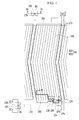
- FIG. 1 is a plan view of an exemplary embodiment of a thin film transistor array panel according to the invention
- FIG. 2 is a cross-sectional view illustrating the thin film transistor array panel taken along line II-II' of FIG. 1
- FIG. 3 is a cross-sectional view illustrating the thin film transistor array panel taken along line III-III of FIG. 1
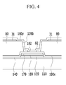
- FIG. 4 is a cross-sectional view illustrating the thin film transistor array panel taken along line IV-IV of FIG. 1 .
- one or more gate line 121 is disposed on an insulation substrate 110.
- Each gate line 121 of a plurality of gate lines 121 includes a wide gate pad portion 129 at a distal end thereof, and a plurality of gate electrodes 124 protruding from a main portion thereof.
- the wide gate pad portion 129 connects the plurality of gate electrodes 124 with another layer of the thin film transistor array panel or an external driving circuit (not shown).
- a gate driving circuit (not illustrated) generating a gate signal may be mounted on a flexible printed circuit film (not illustrated) attached to the insulation substrate 110, or may be directly mounted on the insulation substrate 110.
- a gate conductor includes the gate line 121, the gate electrode 124 and the wide gate pad portion 129.
- the elements of the gate conductor are in a same layer of the thin film transistor array panel, and may have a single layer structure, or a multilayer structure including two or more conductive layers.
- the gate insulating layer 140 is disposed on the gate conductor 121, 124 and 129.
- the gate insulating layer 140 may include an inorganic insulating material, such as silicon nitride (SiNx) or silicon oxide (SiOx).
- a semiconductor 154 is disposed on the gate insulating layer 140.
- Ohmic contacts 163 and 165 are disposed on the semiconductor 154.
- the semiconductor 154 may include an oxide semiconductor. Where the semiconductor 154 is an oxide semiconductor, the ohmic contacts 163 and 165 may be omitted.
- a data conductor including one or more data line 171 and one or more drain electrode 175 is disposed on the ohmic contacts 163 and 165.
- the data line 171 transmits a data signal, and mainly extends in a vertical direction to intersect the gate line 121.
- Each of a plurality of data lines 171 includes a source electrode 173 extending toward a gate electrode 124, and a wide data pad portion 179 for connecting the data line 171 to another layer of the thin film transistor array panel or to an external driving circuit.
- a data driving circuit (not illustrated) for generating a data signal may be mounted on a flexible printed circuit film (not illustrated) attached to the insulation substrate 110, or may be directly mounted on the insulation substrate 110.
- the drain electrode 175 includes an elongated rod-shaped first end portion facing the source electrode 173 with respect to the gate electrode 124, and a wide planar area second end portion opposite to the first end portion.
- a first semiconductor 159 and a first ohmic contact 169 are disposed under the data pad portion 179.
- the first semiconductor 159 and the first ohmic contact 169 may be omitted.
- the data conductor 171, 173, 175 and 179 may have a single layer structure, or a multilayer structure including two or more conductive layers.
- the gate electrode 124, the source electrode 173 and the drain electrode 175 form a thin film transistor ("TFT") together with the semiconductor 154.
- the semiconductor 154 is exposed between the source and drain electrodes 173 and 175, and forms a channel of the TFT.
- the TFT may otherwise be referred to as a switching element.
- the semiconductor 154 may have substantially the same plane shape as those of the data conductor 171, 173, 175, and 179 except for a channel portion of the TFT.
- a first passivation layer 180x is disposed on the data conductor 171, 173, 175 and 179, and the exposed semiconductor 154.
- the first passivation layer 180x may include an organic insulating material or an inorganic insulating material.
- An organic film 80 is disposed on the first passivation layer 180x.
- the organic film 80 has a larger cross-sectional thickness than that of the first passivation layer 180x.
- the organic film 80 may have a substantially flat surface to planarize underlying layers of the TFT array panel.
- a common electrode 131 and a blocking member 31 are disposed on the organic film 80.
- the common electrode 131 and the blocking member 31 may include a transparent conductive material, such as indium tin oxide ("ITO") or indium zinc oxide (“IZO").
- ITO indium tin oxide
- IZO indium zinc oxide
- the common electrode 131 and the blocking member 31 may be in a same layer of the TFT array panel.
- the liquid crystal display includes a display region in which a plurality of pixels is disposed to display an image, and a non-display (e.g., peripheral) region in which the image is not displayed.
- the common electrode 131 is disposed in the display region, and the blocking member 31 is disposed in the peripheral region along with the gate pad portion 129 and the data pad portion 179.
- the organic film 80, and the common electrode 131 and the blocking member 31 disposed on the organic film 80 may have substantially the same plane shape as each other. More particularly, edges or boundaries of the common electrode 131 and the blocking member 31 substantially meet and may be aligned with an edge of the organic film 80, but the invention is not limited thereto. An edge of the organic layer 80 may be exposed by the common electrode 131 and the blocking member 31, such that edges of the common electrode 131 and the blocking member 31 overlap the organic film 80.
- the organic film 80, and the common electrode 131 and the blocking member 31 disposed on the organic film 80 are simultaneously formed (e.g., provided) such as through a single photolithography process.
- a first opening 138 is defined in the organic film 80 and the common electrode 131 at a position overlapping a portion of the drain electrode 175.
- a second opening 139a is defined in the organic film 80 and the blocking member 31 at a position overlapping a portion of the gate pad portion 129, and a third opening 139b is defined in the organic film 80 and the blocking member 31 at a position overlapping a portion of the data pad portion 179.
- a second passivation layer 180y is disposed on the common electrode 131 and the blocking member 31.
- the second passivation layer 180y may include an organic insulating material or an inorganic insulating material.
- a first contact hole 184 is defined in the second passivation layer 180y and the first passivation layer 180x and exposes a portion of the drain electrode 175.
- the first contact hole 184 is disposed inside the first opening 138 defined in the organic film 80 and the common electrode 131.
- the first contact hole 184 is aligned with the first opening 138.
- a second contact hole 181 is defined in the second passivation layer 180y, the first passivation layer 180x and the gate insulating layer 140 and exposes the gate pad portion 129.
- the second contact hole 181 is disposed inside the second opening 139a defined in the organic film 80 and the blocking member 31.
- the second contact hole 181 is aligned with the second opening 139a.
- a third contact hole 182 is defined in the second passivation layer 180y and the first passivation layer 180x and exposes the data pad portion 179.
- the third contact hole 182 is disposed inside the third opening portion 139b defined in the organic film 80 and the blocking member 31.
- the third contact hole 182 is aligned with the third opening 139b.
- a pixel electrode 191, a first contact assistant 81 and a second contact assistant 82 are disposed on the second passivation layer 180y.
- the pixel electrode 191, the first contact assistant 81 and the second contact assistant 82 may include a transparent conductive material, such as ITO or IZO.
- the pixel electrode 191, the first contact assistant 81 and the second contact assistant 82 may be in a same layer of the TFT array panel.
- the pixel electrode 191 is electrically connected with the drain electrode 175 through the first contact hole 184 to receive a data voltage.
- the pixel electrode 191 includes a plurality of branch electrodes 193 generally extended in the vertical direction, parallel to each other and spaced apart from each other, and lower and upper horizontal portions 192 connecting upper and lower end portions of the branch electrodes 193.
- the branch electrodes 193 of the pixel electrode 191 may be parallel to the data lines 171. Where the data lines 171 are bent, the branch electrodes 193 may also be bent and extend along the data lines 171.
- the branch electrodes 193 may be defined by openings or cutouts defined in the pixel electrode 191.
- the first contact assistant 81 is disposed on the gate pad portion 129 exposed through the second contact hole 181, and the second contact assistant 82 is disposed on the data pad portion 179 exposed through the third contact hole 182.
- the pixel electrode 191 receiving the data voltage generates an electric field in a liquid crystal layer disposed on the TFT array panel, together with the common electrode 131 receiving a common voltage.
- the organic film 80, and the common electrode 131 and the blocking member 31 disposed on the organic film 80 may be formed together by using one photo mask. Accordingly, it is possible to reduce or effectively prevent an increase in manufacturing cost of the liquid crystal display. Further, since the organic film 80, and the common electrode 131 and the blocking member 31 disposed on the organic film 80, have substantially the same plane shape, it is possible to reduce or effectively prevent a decrease in a planar area of the common electrode 131 compared to a case where an opening is defined in the common electrode 131 to be wider than an opening defined in the organic film 80.
- the signal line may include the gate line 121 and/or the data line 171.
- any one of the common electrode 131 and the pixel electrode 191 may have the branch electrode, and the other one may have a planar shape, but the invention is not limited thereto.
- an electrode may be a single, unitary, indivisible member and/or disposed on an entire of a substrate, without an opening defined therein.
- the branch electrodes may be defined by openings or cutouts defined in the respective electrode.
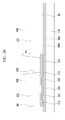
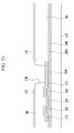
- FIGS. 5 , 8 , 11 , 14 , 17 , 20 , 23 , 26 and 29 are cross-sectional views illustrating an exemplary embodiment of a method of manufacturing the TFT array panel according to the invention, taken along line II-II' of FIG. 1 .
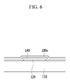
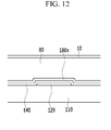
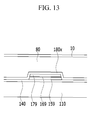
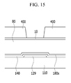
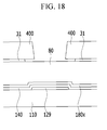
- FIGS. 6 , 9 , 12 , 15 , 18 , 21 , 24 , 27 and 30 are cross-sectional views illustrating the exemplary embodiment of the method of manufacturing the TFT array panel according to the invention, taken along line III-III of FIG. 1 .
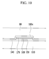
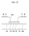
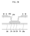
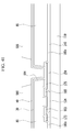
- FIGS. 7 , 10 , 13 , 16 , 19 , 22 , 25 , 28 and 31 are cross-sectional views illustrating the exemplary embodiment of the method of manufacturing the TFT array panel according to the invention, taken along line IV-IV of FIG. 1 .
- the gate conductor 121, 124 and 129 including the gate line 121, the gate electrode 124 and the gate pad portion 129 is formed (e.g., provided) on the insulation substrate 110, and the gate insulating layer 140 is deposited on the gate conductor 121, 124 and 129.
- the semiconductor 154, the first semiconductor 159, the ohmic contacts 163 and 165, the first ohmic contact 169 and the data conductor 171, 173, 175, and 179 including the data line 171, the source electrode 173, the drain electrode 175 and the data pad portion 179 are formed on the gate insulating layer 140.
- the first passivation layer 180x is deposited on the data conductor 171, 173, 175 and 179, and the exposed semiconductor 154.
- the organic film 80 is deposited on the first passivation layer 180x.
- a first conductive layer 10 is deposited on the organic film 80.
- a photosensitive film is deposited and then exposed and developed to form a first photosensitive film pattern 400.
- the first conductive layer 10 is etched by using the first photosensitive film pattern 400 as a mask to form the common electrode 131 and the blocking member 31.
- the first opening 138 at the position overlapping the part of the drain electrode 175, the second opening 139a at the position overlapping the part of the gate pad portion 129, and the third opening 139b at the position overlapping the part of the data pad portion 179 are defined in the organic film 80 such as through ashing the organic film 80 by using the common electrode 131 and the blocking member 31 as a mask.
- a portion of the first photosensitive film pattern 400 is ashed together with the organic film 80, so that a height of the first photosensitive film pattern 400 is decreased from an original height thereof to be a first height H1.
- the first height H1 may be approximately 2.5 micrometers ( ⁇ m) or more.
- the first height H1 of the first photosensitive film pattern 400 is maintained, so that it is possible to prevent haze of the common electrode 131 and the blocking member 31 disposed under the organic film 80.
- the first photosensitive film pattern 400 is removed.
- the second passivation layer 180y is deposited on the organic film 80 and the blocking member 31.
- the first contact hole 184 exposing a portion of the drain electrode 175 is defined in the second passivation layer 180y and the first passivation layer 180x
- the second contact hole 181 exposing the gate pad portion 129 is defined in the second passivation layer 180y
- the first passivation layer 180x the first passivation layer 180x
- the gate insulating layer 140 and the third contact hole 182 exposing the data pad portion 179 is defined in the second passivation layer 180y and the first passivation layer 180x.
- the first contact hole 184 is disposed inside the first opening 138 defined in the organic film 80 and the common electrode 131, the second contact hole 181 is disposed inside the second opening 139a defined in the organic film 80 and the blocking member 31, and the third contact hole 182 is disposed inside the third opening 139b defined in the organic film 80 and the blocking member 31.
- the pixel electrode 191, the first contact assistant 81 and the second contact assistant 82 are formed on the second passivation layer 180y.
- the pixel electrode 191 is electrically connected with the drain electrode 175 through the first contact hole 184.
- the first contact assistant 81 is disposed on the gate pad portion 129 exposed through the second contact hole 181, and the second contact assistant 82 is disposed on the data pad portion 179 exposed through the third contact hole 182.
- the organic film 80, and the common electrode 131 and the blocking member 31 disposed on the organic film 80 are formed together by using one photo mask. Accordingly, it is possible to reduce or effectively prevent an increase of manufacturing cost of the liquid crystal display.
- FIG. 32 is a plan view of another exemplary embodiment of a TFT array panel according to the invention
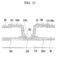
- FIG. 33 is a cross-sectional view illustrating the TFT array panel taken along line XXXIII- XXXIII of FIG. 32 .
- the exemplary embodiment of TFT array panel according to the invention is substantially similar to the exemplary embodiment of the TFT array panel described with reference to FIGS. 1 to 4 .
- the exemplary embodiment of the TFT array panel in FIGS. 32 and 33 includes one or more common voltage line 125 disposed in and/or on a same layer as that of the gate line 121.
- the common voltage line 125 may transmit a predetermined voltage, such as a common voltage, and may be generally extended in a horizontal direction, and substantially parallel to the gate line 121.
- the common voltage line 125 may include an expansion portion 126.
- a gate insulating layer 140, a first passivation layer 180x, an organic film 80, a common electrode 131 and a second passivation layer 180y are sequentially disposed on the common voltage line 125.
- a fourth opening 139c is defined in the organic film 80 and the common electrode 131 at a position overlapping the expansion portion 126 of the common voltage line 125.
- a fourth contact hole 185 exposing the expansion portion 126 of the common voltage line 125 is defined in the second passivation layer 180y, the first passivation layer 180x and the gate insulating layer 140, and a fifth contact hole 186 exposing a portion of the common electrode 131 is defined in the second passivation layer 180y.
- the fourth contact hole 185 is disposed inside the fourth opening 139c defined in the organic film 80 and the common electrode 131.
- a first connecting member 93 is disposed on the second passivation layer 180y.
- the first connecting member 93 is in and/or on a same layer as that of a pixel electrode 191 and is spaced apart from the pixel electrode 191.
- the first connecting member 93 connects the expansion portion 126 of the common voltage line 125 and the common electrode 131 with each other by covering the expansion portion 126 of the common voltage line 125 exposed through the fourth contact hole 185 and the common electrode 131 exposed through the fifth contact hole 186. Accordingly, a common voltage transmitted through the common voltage line 125 is transmitted to the common electrode 131.
- the exemplary embodiment of the TFT array panel according to the invention includes the common voltage line 125 disposed in the same layer as that of the gate line 121, but the invention is not limited thereto.
- a common voltage line may be disposed in a same layer as that of a data line 171. Where the common voltage line is in the same layer as the data line 171, the contact hole exposing the expansion portion of the common voltage line may be defined in the second passivation layer 180y and the first passivation layer 180x. Further, the common voltage line may be extended along the data line 171 to be side-by-side (e.g., adjacent with) the data line 171.
- FIGS. 34 to 37 Still another exemplary embodiment of a TFT array panel according to the invention will be described with reference to FIGS. 34 to 37 .
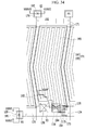
- FIG. 34 is a plan view of still another exemplary embodiment of a TFT array panel according to the invention
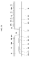
- FIG. 35 is a cross-sectional view illustrating the TFT array panel taken along line XXXV-XXXV' of FIG. 34
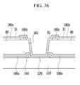
- FIG. 36 is a cross-sectional view illustrating the TFT array panel taken along line XXXVI-XXXVI of FIG. 34
- FIG. 37 is a cross-sectional view illustrating the TFT array panel taken along line XXXVII-XXXVII of FIG. 34 .
- one or more gate line 121 is disposed on an insulation substrate 110.
- the gate line 121 includes a gate electrode 124 and a gate pad portion 129 extending from a main portion thereof.
- a gate insulating layer 140 is disposed on a gate conductor 121, 124 and 129.
- a semiconductor 154 is disposed on the gate insulating layer 140.
- Ohmic contacts 163 and 165 are disposed on the semiconductor 154.
- the semiconductor 154 may include an oxide semiconductor, and where the semiconductor 154 is an oxide semiconductor, the ohmic contacts 163 and 165 may be omitted.
- One or more data line 171 and one or more drain electrode 175 is disposed on the ohmic contacts 163 and 165.
- the data line 171 includes a source electrode 173 protruded from a main portion thereof and extending toward the gate electrode 124, and a data pad portion 179.
- a first semiconductor 159 and a first ohmic contact 169 are disposed under the data pad portion 179.
- the first semiconductor 159 and the first ohmic contact 169 may be omitted.
- a first passivation layer 180x is disposed on a data conductor 171, 173, 175, and 179 and the exposed semiconductor 154, and the first passivation layer 180x may include an organic insulating material or an inorganic insulating material.
- An organic film 80 is disposed on the first passivation layer 180x.
- the organic film 80 may be relatively thicker than the first passivation layer 180x in a cross-sectional direction, and may have a flat surface.
- a common electrode 131 and a blocking member 31 are disposed on the organic film 80.
- the common electrode 131 and the blocking member 31 may include a transparent conductive material, such as ITO or IZO.
- a first opening 138 is defined in the common electrode 131 at a position overlapping a portion of the drain electrode 175.
- the common electrode 131 is disposed in a display region of the liquid crystal display in which a plurality of pixels is disposed to display an image
- the blocking member 31 is disposed in a peripheral region of the liquid crystal display in which the gate pad portion 129 and the data pad portion 179 are disposed.
- a second passivation layer 180y is disposed on the common electrode 131 and the blocking member 31.
- a plane shape of the second passivation layer 180y is substantially the same as a plane shape of the common electrode 131 and the blocking member 31. That is, the second passivation layer 180y overlaps edges of the common electrode 131 and the blocking member 31.
- the second passivation layer 180y, the common electrode 131 and the blocking member 31 may be formed (e.g., provided) together by using one photo mask, such that the plane shape of the second passivation layer 180y is substantially the same as the plane shape of the common electrode 131 and the blocking member 31.
- an edge of the second passivation layer 180y protrudes further than an edge of the common electrode 131 and the blocking member 31, at openings where the drain electrode 175, the gate pad portion 129 and the data pad portion 179 are exposed. That is, the common electrode 131 and the blocking member 31, and the second passivation layer 180y disposed on the common electrode 131 and the blocking member 31, have an inverse taper structure in which an upper layer protrudes further towards the openings than a lower layer.
- a third passivation layer 180z is disposed at the edges of the common electrode 131 and the blocking member 31, such as adjacent and/or contacting the edges of the common electrode 131 and the blocking member 31.
- the third passivation layer 180z is disposed under the second passivation layer 180y, and is disposed to surround the openings where the edges of the common electrode 131 and the blocking member 31 are disposed.
- An edge of the third passivation layer 180z is disposed to substantially meet or coincide with the edge of the second passivation layer 180y.
- the side surfaces at the edges of the second and third passivation layers 180y and 180z at the openings may be aligned or coplanar with each other.
- the common electrode 131 and the blocking layer 31 expose an edge of the second passivation layer 180y.
- the second and third passivation layers 180y and 180z expose an edge of the organic film 80.
- the exemplary embodiment of the TFT array panel according to the invention includes a third passivation layer 180z disposed under the second passivation layer 180y and surrounding openings at the edges of the common electrode 131 and the blocking member 31, so that the common electrode 131, the blocking member 31 and the third passivation layer 180z are disposed on a same layer of the TFT array panel, and the second passivation layer 180y disposed on the common electrode 131, the blocking member 31 and the third passivation layer 180z removes or compensates for the inverse taper structure formed by the second passivation layer 180y disposed on the common electrode 131 and the blocking member 31.
- a first contact hole 184 exposing a portion of the drain electrode 175 is defined in the organic film 80 and the first passivation layer 180x.
- a second contact hole 181 exposing a portion of the gate pad portion 129 is defined in the organic film 80, the first passivation layer 180x and the gate insulating layer 140.
- a third contact hole 182 exposing a data pad portion 179 is defined in the organic film 80 and the first passivation layer 180x.
- a pixel electrode 191, a first contact assistant 81 and a second contact assistant 82 are disposed on the second passivation layer 180y and the third passivation layer 180z.
- the pixel electrode 191, the first contact assistant 81 and the second contact assistant 82 may include a transparent conductive material, such as ITO or IZO.
- the pixel electrode 191 is electrically connected with the drain electrode 175 through the first contact hole 184 to receive a data voltage.
- the pixel electrode 191 includes a plurality of branch electrodes 193 generally extended in the vertical direction, parallel to each other and spaced apart from each other, and lower and upper horizontal portions 192 connecting upper and lower end portions of the branch electrodes 193.
- the branch electrodes 193 of the pixel electrode 191 may be parallel to the data lines 171. Where the data lines 171 are bent, the branch electrodes 193 may also be bent and extend along the data lines 171.
- the branch electrodes 193 may be defined by openings or cutouts defined in the pixel electrode 191.
- the first contact assistant 81 is disposed on the gate pad portion 129 exposed through the second contact hole 181, and the second contact assistant 82 is disposed on the data pad portion 179 exposed through the third contact hole 182.
- the pixel electrode 191 receiving the data voltage generates an electric field in a liquid crystal layer disposed on the TFT array panel, together with the common electrode 131 receiving a common voltage.
- the second passivation layer 180y, the common electrode 131 and the blocking member 31 may be formed together by using one photo mask. Accordingly, it is possible to reduce or effectively prevent an increase of manufacturing cost of the liquid crystal display. Further, it is possible to reduce or effectively prevent static electricity and the like introduced from outside the liquid crystal display from being introduced in a signal line by forming the blocking member 31 around the gate pad portion 129 and the data pad portion 179.
- the signal line may include the gate line 121 and/or the data line 171.
- any one of the common electrode 131 and the pixel electrode 191 may have the branch electrode, and the other one may have a planar shape, but the invention is not limited thereto.
- an electrode may be a single, unitary, indivisible member and/or disposed on an entire of a substrate, without an opening defined therein.
- the branch electrodes may be defined by openings or cutouts defined in the respective electrode.
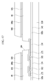
- FIGS. 38 , 41 , 44 , 47 , 50 and 53 are cross-sectional views illustrating an exemplary embodiment of a method of manufacturing the TFT array panel according to the invention, taken along line XXXV- XXXV' of FIG. 34 .
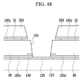
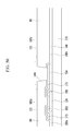
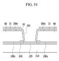
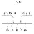
- FIGS. 39 , 42 , 45 , 48 , 51 and 54 are cross-sectional views illustrating the exemplary embodiment of the method of manufacturing the TFT array panel according to the invention, taken along line XXXVI-XXXVI of FIG. 34 .
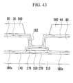
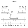
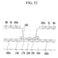
- FIGS. 40 , 43 , 46 , 49 , 52 and 55 are cross-sectional views illustrating the exemplary embodiment of the method of manufacturing the TFT array panel according to the invention, taken along line XXXVII-XXXVII of FIG. 34 .
- the gate conductor 121, 124 and 129 including the gate lines 121, the gate electrodes 124 and the gate pad portions 129 is formed (e.g., provided) on the insulation substrate 110, and the gate insulating layer 140 is deposited on the gate conductor 121, 124 and 129.
- the semiconductor 154, the first semiconductor 159, the ohmic contacts 163 and 165, the first ohmic contact 169 and the data conductor 171, 173, 175, and 179 including the data lines 171, the source electrodes 173, the drain electrodes 175, and the data pad portions 179 are formed on the gate insulating layer 140.
- the first passivation layer 180x is deposited on the data conductor 171, 173, 175, and 179, and the exposed semiconductor 154.
- the organic film 80 is formed on the first passivation layer 180x, and the first passivation layer 180x and the gate insulating layer 140 are etched to define the first contact hole 184 exposing a portion of the drain electrode 175, the second contact hole 181 exposing a portion of the gate pad portion 129, and the third contact hole 182 a portion the data pad portion 179.
- a second conductive layer 30 is deposited on the organic film 80, and a first insulating layer 40 is deposited on the second conductive layer 30.
- a photosensitive film is deposited on the first insulating layer 40 and then is exposed and developed to form a second photosensitive film pattern 500.
- the first insulating layer 40 is etched by using the second photosensitive film pattern 500 as an etching mask to form the second passivation layer 180y.
- the second conducive layer 30 is etched by using the second photosensitive film pattern 500 as an etching mask to form the common electrode 131 and the blocking member 31.
- An etchant capable of etching only the second conductive layer 30 and incapable of etching the drain electrode 175, the gate pad portion 129 and the data pad portion 179 is used.
- edges of the common electrode 131 and the blocking member 31 are disposed at an inner side of the edge of the second passivation layer 180y by sufficiently etching the common electrode 131 and the blocking member 31. Accordingly, the edge of the second passivation layer 180y protrudes further toward the first, second and third contact holes 184, 181 and 182 than the edges of the common electrode 131 and the blocking member 31.
- the second photosensitive film pattern 500 is removed by ashing and the like.
- a second insulating layer 50 having a sufficient thickness is deposited on the second passivation layer 180y, and between the organic film 80 and the overhanging second passivation layer 180y at the first, second and third contact holes 184, 181 and 182.
- the third passivation layer 180z surrounding the edges of the common electrode 131 and the blocking member 31 is formed by removing the second passivation layer 180y and the second insulating layer 50 disposed in the contact holes 184, 181 and 182 by dry-etching the second insulating layer 50.
- the common electrode 131 and the blocking member 31, and the second passivation layer 180y disposed on the common electrode 131 and the blocking member 31, are formed together by using one photo mask.
- the third passivation layer 180z disposed under the second passivation layer 180y and surrounding the edges of the common electrode 131 and the blocking member 31 is formed, so that the common electrode 131, the blocking member 31 and the third passivation layer 180z disposed in a the same layer as the TFT array panel and the second passivation layer 180y disposed on the common electrode 131, the blocking member 31 and the third passivation layer 180z do not have an inverse taper structure.
- the pixel electrode 191, the first contact assistant 81 and the second contact assistant 82 are formed on the second passivation layer 180y and the third passivation layer 180z.
- the pixel electrode 191 is electrically connected with the drain electrode 175 through the first contact hole 184.
- the first contact assistant 81 is disposed on the gate pad portion 129 exposed through the second contact hole 181, and the second contact assistant 82 is disposed on the data pad portion 179 exposed through the third contact hole 182.
- the third passivation layer 180 surrounding the edges of the common electrode 131 and the blocking member 31 is formed, so that the common electrode 131, the blocking member 31 and the third passivation layer 180z disposed in the same layer of the TFT array panel, and the second passivation layer 180y disposed on the common electrode 131, the blocking member 31 and the third passivation layer 180z do not have the inverse taper structure. Accordingly, it is possible to reduce or effectively prevent a short circuit of the pixel electrode 191 disposed on the second passivation layer 180y and the third passivation layer 180z, the first contact assistant 81, and the second contact assistant 82 due to the inverse taper structure.
- the common electrode 131 and the blocking member 31, and the second passivation layer 180y disposed on the common electrode 131 and the blocking member 31, are formed together by using one photo mask. Accordingly, it is possible to reduce or effectively prevent an increase of manufacturing cost of the liquid crystal display.
- the characteristics of one or more of the previously described exemplary embodiment of a TFT array panel are applicable to a liquid crystal display in which the common electrode and the pixel electrode as the two field generating electrodes are disposed on the TFT display panel including only one single substrate.
- an electrode may be a single, unitary, indivisible member and/or disposed on an entire of a substrate, without an opening defined therein.
- the branch electrodes may be defined by openings or cutouts defined in the respective electrode.
- a passivation layer disposed between a first field generating electrode and a second field generating electrode overlapping each other is thin and includes a transparent photosensitive organic material.
- the passivation layer is used as a photosensitive film when providing the first field generating electrode, so that the passivation layer and the first field generating electrode disposed under the passivation layer may be formed together by using one photo mask. Accordingly, it is possible to prevent an increase in manufacturing cost of the thin film transistor array panel.
Landscapes
- Physics & Mathematics (AREA)
- Nonlinear Science (AREA)
- Mathematical Physics (AREA)
- Chemical & Material Sciences (AREA)
- Crystallography & Structural Chemistry (AREA)
- General Physics & Mathematics (AREA)
- Optics & Photonics (AREA)
- Engineering & Computer Science (AREA)
- Microelectronics & Electronic Packaging (AREA)
- Geometry (AREA)
- Liquid Crystal (AREA)
Abstract
Description
- The invention relates to a thin film transistor array panel and a method of manufacturing the same.
- A liquid crystal display, is one of the most widely used flat panel displays. The liquid crystal display is a display device which adjusts a quantity of penetrated light by applying a voltage to an electrode of a display panel and re-arranges liquid crystal molecules of a liquid crystal layer of the display panel.
- The liquid crystal display may be manufactured to be relatively thin. However, the liquid crystal display has a disadvantage in that side visibility thereof is worse than front visibility, so that various types of liquid crystal arrangements and driving methods have been developed in order to overcome the disadvantage.
- One or more exemplary embodiment of the invention provides a liquid crystal display capable of reducing or effectively preventing an increase in manufacturing cost even when two field generating electrodes are disposed on a single substrate of one display panel, and a method of manufacturing the same.
- An exemplary embodiment of the invention provides a thin film transistor array panel, including: an insulation substrate; a gate line and a data line on the insulation substrate; a first passivation layer on the gate line and the data line; an organic layer on the first passivation layer; a first electrode on the organic layer; a second passivation layer on the first electrode; and a second electrode on the second passivation layer. An edge of the organic layer is exposed by an edge of the first electrode.
- The gate line may include a gate pad portion, the data line may include a data pad portion, and the thin film transistor array panel may further include a blocking member at a peripheral region of the gate pad portion and the data pad portion, and on the organic layer.
- The blocking member may be in a same layer as the first electrode.
- The blocking member at the peripheral region of the gate pad portion and the data pad portion may overlap an edge of the organic layer at the peripheral region of the gate pad portion and the data pad portion.
- One of the first electrode and the second electrode may have a planar shape, and the other of the first electrode and the second electrode includes a branch electrode.
- The thin film transistor array panel may further include a common voltage line in a same layer as the gate line or the data line. An opening may be defined in the organic layer and the first electrode and expose a portion of the common voltage line, a contact hole may be defined in the second passivation layer and expose the first electrode, and the thin film transistor array panel may further include a connecting member covering the common voltage line exposed through the opening and the first electrode exposed through the contact hole.
- The connecting member may be spaced apart from the second electrode, and may be in a same layer as the second electrode.
- Another exemplary embodiment of the invention provides a thin film transistor array panel, including: an insulation substrate; a gate line and a data line on the insulation substrate; a first passivation layer on the gate line and the data line; an organic layer on the first passivation layer; a first electrode on the organic layer; a second passivation layer on the first electrode; a second electrode on the second passivation layer; and a third passivation layer covering a side surface of an edge of the first electrode. The second passivation layer overlaps the side surface and the edge of the first electrode in a plan view.
- The first electrode exposes an edge of the second passivation layer.
- An edge of the third passivation layer may substantially coincide with the edge of the second passivation layer.
- The gate line may include a gate pad portion, the data line may include a data pad portion, and the thin film transistor array panel may further include a blocking member at a peripheral region of the gate pad portion and the data pad portion, and on the organic layer. The second passivation layer at the peripheral region of the gate pad portion and the data pad portion may overlap an edge of the blocking member at the peripheral region of the gate pad portion and the data pad portion.
- The blocking member exposes an edge of the second passivation layer at the peripheral region of the gate pad portion and the data pad portion.
- The third passivation layer may cover a side surface at the edge of the blocking member, and an edge of the third passivation layer at the peripheral region of the gate pad portion and the data pad portion may substantially coincide with the edge of the second passivation layer at the peripheral region of the gate pad portion and the data pad portion.
- Yet another exemplary embodiment of the invention provides a method of manufacturing a thin film transistor array panel, including: providing a gate line and a data line on an insulation substrate; providing a first passivation layer on the gate line and the data line; providing an organic layer on the first passivation layer; depositing a conductive layer on the organic layer; providing a photosensitive film pattern on the conductive layer; providing a first electrode by etching the conductive layer by using the photosensitive film pattern as a mask; providing an organic film by etching the organic layer by using the photosensitive film pattern as a mask; providing the second passivation layer on the first electrode; and providing a second electrode on the second passivation layer. An edge of the organic layer is exposed by the first electrode.
- The providing of the gate line may include providing a gate pad portion connected to the gate line, the providing of the data line may include providing a data pad portion connected to the data line, and the method may further include providing a blocking member at a peripheral region of the gate pad portion and the data pad portion by etching the conductive layer by using the photosensitive film pattern as the mask.
- The blocking member at the peripheral region of the gate pad portion and the data pad portion may expose an edge of the organic layer at the peripheral region of the gate pad portion and the data pad portion.
- In the method of manufacturing the thin film transistor array panel, one of the first electrode and the second electrode may have a planar shape, and the other the first electrode and the second electrode may include a branch electrode.
- The providing of the gate lines or the providing of the data lines may further include providing a common voltage line. The providing of the organic film and the first electrode may further include defining an opening exposing a portion of the common voltage line, the providing of the second passivation layer may further include defining a contact hole exposing the first electrode, and the method may further include providing a connecting member covering the common voltage line exposed through the opening and the first electrode exposed through the contact hole.
- The connecting member may be in a same layer as that of the second electrode.
- Still another exemplary embodiment of the invention provides a method of manufacturing a thin film transistor array panel, including: providing a gate line and a data line on an insulation substrate; providing a first passivation layer on the gate line and the data line; providing an organic layer on the first passivation layer; depositing a conductive layer on the organic layer; depositing an insulating layer on the conductive layer; providing a photosensitive film pattern on the insulating layer; providing a second passivation layer by etching the insulating layer by using the photosensitive film pattern as a mask; providing a first electrode by etching the conductive layer by using the photosensitive film pattern as a mask; providing a third passivation layer covering a side surface of an edge of the first electrode; and providing a second electrode on the second passivation layer and the third passivation layer.
- The providing the first electrode may include etching the conductive layer so that the first electrode exposes an edge of the second passivation layer.
- The providing of the third passivation layer may include providing the third passivation layer so that an edge of the third passivation layer substantially coincides with the edge of the second passivation layer.
- The providing of the gate line may include providing the gate pad portion connected to the gate line, the providing of the data line may include providing a data pad portion connected to the data line, and the method may further include providing a blocking member at the peripheral region of the gate pad portion and the data pad portion by etching the conductive layer by using the photosensitive film pattern as the mask. In the method of manufacturing the thin film transistor array panel, the second passivation layer at the peripheral region of the gate pad portion and the data pad portion may overlap an edge of the blocking member at the peripheral region of the gate pad portion and the data pad portion.
- In the method of manufacturing the thin film transistor array panel, the blocking member exposes an edge of the second passivation layer at the peripheral region of the gate pad portion and the data pad portion.
- The providing of the third passivation layer may further include providing a fourth passivation layer covering a side surface at the edge of the blocking member, and an edge of the fourth passivation layer at the peripheral region of the gate pad portion and the data pad portion may substantially coincide with the edge of the second passivation layer at the peripheral region of the gate pad portion and the data pad portion.
- According to one or more exemplary embodiment of the thin film transistor array panel and the method of manufacturing the same according to the invention, it is possible to reduce or effectively prevent an increase in manufacturing cost even when providing two field generating electrodes on a single substrate of one display panel.
- The above and other features of this disclosure will become more apparent by describing in further detail exemplary embodiments thereof with reference to the accompanying drawings, in which:
-
FIG. 1 is a plan view of an exemplary embodiment of a thin film transistor array panel according to the invention. -
FIG. 2 is a cross-sectional view illustrating the thin film transistor array panel taken along line II-II' ofFIG. 1 . -
FIG. 3 is a cross-sectional view illustrating the thin film transistor array panel taken along line III-III ofFIG. 1 . -
FIG. 4 is a cross-sectional view illustrating the thin film transistor array panel taken along line IV-IV ofFIG. 1 . -
FIGS. 5 ,8 ,11 ,14 ,17 ,20 ,23 ,26 and29 are cross-sectional views illustrating an exemplary embodiment of a method of manufacturing the thin film transistor array panel according to the invention, taken along line II-II' ofFIG. 1 . -
FIGS. 6 ,9 ,12 ,15 ,18 ,21 ,24 ,27 and30 are cross-sectional views sequentially illustrating the exemplary embodiment of the method of manufacturing the thin film transistor array panel according to the invention, I taken along line III-III ofFIG. 1 . -
FIGS. 7 ,10 ,13 ,16 ,19 ,22 ,25 ,28 and31 are cross-sectional views sequentially illustrating the exemplary embodiment of the method of manufacturing the thin film transistor array panel according to the invention, taken along line IV-IV ofFIG. 1 . -
FIG. 32 is a plan view of another exemplary embodiment of a thin film transistor array panel according to the invention. -
FIG. 33 is a cross-sectional view illustrating the thin film transistor array panel taken along line XXXIII- XXXIII ofFIG. 32 . -
FIG. 34 is a plan view of still another exemplary embodiment of a thin film transistor array panel according to the invention. -
FIG. 35 is a cross-sectional view illustrating the thin film transistor array panel taken along line XXXV-XXXV' ofFIG. 34 . -
FIG. 36 is a cross-sectional view illustrating the thin film transistor array panel taken along line XXXVI-XXXVI ofFIG. 34 . -
FIG. 37 is a cross-sectional view illustrating the thin film transistor array panel taken along line XXXVII-XXXVII ofFIG. 34 . -
FIGS. 38 ,41 ,44 ,47 ,50 ,53 and56 are cross-sectional views sequentially illustrating an exemplary embodiment of a method of manufacturing the thin film transistor array panel according to the invention, taken along line XXXV- XXXV' ofFIG. 34 . -
FIGS. 39 ,42 ,45 ,48 ,51 ,54 and57 are cross-sectional views sequentially illustrating the exemplary embodiment of the method of manufacturing the thin film transistor array panel according to the invention, taken along line XXXVI-XXXVI ofFIG. 34 . -
FIGS. 40 ,43 ,46 ,49 ,52 ,55 and58 are cross-sectional views sequentially illustrating the exemplary embodiment of the method of manufacturing the thin film transistor array panel according to the invention, taken along line XXXVII-XXXVII ofFIG. 34 . - The invention will be described more fully hereinafter with reference to the accompanying drawings, in which exemplary embodiments of the invention are shown. As those skilled in the art would realize, the described embodiments may be modified in various different ways, all without departing from the scope of the invention.
- In the drawings, the thickness of layers, films, panels, regions, etc., are exaggerated for clarity. Like reference numerals designate like elements throughout the specification. It will be understood that when an element such as a layer, film, region, or substrate is referred to as being "on" another element, it can be directly on the other element or intervening elements may also be present. In contrast, when an element is referred to as being "directly on" another element, there are no intervening elements present. As used herein, connected may refer to elements being physically and/or electrically connected to each other. As used herein, the term "and/or" includes any and all combinations of one or more of the associated listed items.
- It will be understood that, although the terms first, second, third, etc., may be used herein to describe various elements, components, regions, layers and/or sections, these elements, components, regions, layers and/or sections should not be limited by these terms. These terms are only used to distinguish one element, component, region, layer or section from another element, component, region, layer or section. Thus, a first element, component, region, layer or section discussed below could be termed a second element, component, region, layer or section without departing from the teachings of the invention.
- Spatially relative terms, such as "lower," "under," "above," "upper" and the like, may be used herein for ease of description to describe the relationship of one element or feature to another element(s) or feature(s) as illustrated in the figures. It will be understood that the spatially relative terms are intended to encompass different orientations of the device in use or operation, in addition to the orientation depicted in the figures. For example, if the device in the figures is turned over, elements described as "under" relative to other elements or features would then be oriented "above" relative to the other elements or features. Thus, the exemplary term "under" can encompass both an orientation of above and below. The device may be otherwise oriented (rotated 90 degrees or at other orientations) and the spatially relative descriptors used herein interpreted accordingly.
- The terminology used herein is for the purpose of describing particular embodiments only and is not intended to be limiting of the invention. As used herein, the singular forms "a," "an" and "the" are intended to include the plural forms as well, unless the context clearly indicates otherwise. It will be further understood that the terms "comprises," "comprising," "includes" and/or "including," when used in this specification, specify the presence of stated features, integers, operations, elements, and/or components, but do not preclude the presence or addition of one or more other features, integers, steps, operations, elements, components, and/or groups thereof.
- Embodiments of the invention are described herein with reference to cross-section illustrations that are schematic illustrations of idealized embodiments (and intermediate structures) of the invention. As such, variations from the shapes of the illustrations as a result, for example, of manufacturing techniques and/or tolerances, are to be expected. Thus, embodiments of the invention should not be construed as limited to the particular shapes of regions illustrated herein but are to include deviations in shapes that result, for example, from manufacturing.
- Unless otherwise defined, all terms (including technical and scientific terms) used herein have the same meaning as commonly understood by one of ordinary skill in the art to which this invention belongs. It will be further understood that terms, such as those defined in commonly used dictionaries, should be interpreted as having a meaning that is consistent with their meaning in the context of the relevant art and will not be interpreted in an idealized or overly formal sense unless expressly so defined herein.
- All methods described herein can be performed in a suitable order unless otherwise indicated herein or otherwise clearly contradicted by context. The use of any and all examples, or exemplary language (e.g., "such as"), is intended merely to better illustrate the invention and does not pose a limitation on the scope of the invention unless otherwise claimed. No language in the specification should be construed as indicating any non-claimed element as essential to the practice of the invention as used herein.
- As a method of implementing a wide viewing angle, a liquid crystal display includes a display panel in which field generating electrodes such as a pixel electrode and a common electrode are disposed on one single substrate of the display panel has attracted attention.
- According to the liquid crystal display having the aforementioned structural elements, a plurality of cutout portions are defined in at least one of the two field generating electrodes among the pixel electrode and the common electrode therein, and the respective field generating electrode includes a plurality of branch electrodes defined by the plurality of cutout portions. Where the two field generating electrodes are disposed in one display panel including the one single substrate, in order to form each field generating electrode in a manufacturing process of the display panel, different photo masks are necessary and thus manufacturing cost is undesirably increased. Therefore, there remains a need for an improved display device and method of manufacturing thereof, which is simplified and has a reduced cost.
- First, an exemplary embodiment of a thin film transistor array panel of a liquid crystal display according to the invention will be described with reference to
FIGS. 1 to 4 .FIG. 1 is a plan view of an exemplary embodiment of a thin film transistor array panel according to the invention,FIG. 2 is a cross-sectional view illustrating the thin film transistor array panel taken along line II-II' ofFIG. 1 ,FIG. 3 is a cross-sectional view illustrating the thin film transistor array panel taken along line III-III ofFIG. 1 , andFIG. 4 is a cross-sectional view illustrating the thin film transistor array panel taken along line IV-IV ofFIG. 1 . - Referring to
FIGS. 1 to 4 , one ormore gate line 121 is disposed on aninsulation substrate 110. - Each
gate line 121 of a plurality ofgate lines 121 includes a widegate pad portion 129 at a distal end thereof, and a plurality ofgate electrodes 124 protruding from a main portion thereof. The widegate pad portion 129 connects the plurality ofgate electrodes 124 with another layer of the thin film transistor array panel or an external driving circuit (not shown). A gate driving circuit (not illustrated) generating a gate signal may be mounted on a flexible printed circuit film (not illustrated) attached to theinsulation substrate 110, or may be directly mounted on theinsulation substrate 110. - A gate conductor includes the
gate line 121, thegate electrode 124 and the widegate pad portion 129. The elements of the gate conductor are in a same layer of the thin film transistor array panel, and may have a single layer structure, or a multilayer structure including two or more conductive layers. - The
gate insulating layer 140 is disposed on thegate conductor gate insulating layer 140 may include an inorganic insulating material, such as silicon nitride (SiNx) or silicon oxide (SiOx). - A
semiconductor 154 is disposed on thegate insulating layer 140.Ohmic contacts semiconductor 154. - The
semiconductor 154 may include an oxide semiconductor. Where thesemiconductor 154 is an oxide semiconductor, theohmic contacts - A data conductor including one or
more data line 171 and one ormore drain electrode 175 is disposed on theohmic contacts - Referring to
FIG. 1 , thedata line 171 transmits a data signal, and mainly extends in a vertical direction to intersect thegate line 121. Each of a plurality ofdata lines 171 includes asource electrode 173 extending toward agate electrode 124, and a widedata pad portion 179 for connecting thedata line 171 to another layer of the thin film transistor array panel or to an external driving circuit. A data driving circuit (not illustrated) for generating a data signal may be mounted on a flexible printed circuit film (not illustrated) attached to theinsulation substrate 110, or may be directly mounted on theinsulation substrate 110. - In the plan view, the
drain electrode 175 includes an elongated rod-shaped first end portion facing thesource electrode 173 with respect to thegate electrode 124, and a wide planar area second end portion opposite to the first end portion. - A
first semiconductor 159 and a firstohmic contact 169 are disposed under thedata pad portion 179. In an alternative exemplary embodiment, thefirst semiconductor 159 and the firstohmic contact 169 may be omitted. - The
data conductor - The
gate electrode 124, thesource electrode 173 and thedrain electrode 175 form a thin film transistor ("TFT") together with thesemiconductor 154. Thesemiconductor 154 is exposed between the source and drainelectrodes semiconductor 154 may have substantially the same plane shape as those of thedata conductor - A
first passivation layer 180x is disposed on thedata conductor semiconductor 154. Thefirst passivation layer 180x may include an organic insulating material or an inorganic insulating material. - An
organic film 80 is disposed on thefirst passivation layer 180x. Theorganic film 80 has a larger cross-sectional thickness than that of thefirst passivation layer 180x. Theorganic film 80 may have a substantially flat surface to planarize underlying layers of the TFT array panel. - A
common electrode 131 and a blockingmember 31 are disposed on theorganic film 80. Thecommon electrode 131 and the blockingmember 31 may include a transparent conductive material, such as indium tin oxide ("ITO") or indium zinc oxide ("IZO"). Thecommon electrode 131 and the blockingmember 31 may be in a same layer of the TFT array panel. - The liquid crystal display includes a display region in which a plurality of pixels is disposed to display an image, and a non-display (e.g., peripheral) region in which the image is not displayed. The
common electrode 131 is disposed in the display region, and the blockingmember 31 is disposed in the peripheral region along with thegate pad portion 129 and thedata pad portion 179. - The
organic film 80, and thecommon electrode 131 and the blockingmember 31 disposed on theorganic film 80, may have substantially the same plane shape as each other. More particularly, edges or boundaries of thecommon electrode 131 and the blockingmember 31 substantially meet and may be aligned with an edge of theorganic film 80, but the invention is not limited thereto. An edge of theorganic layer 80 may be exposed by thecommon electrode 131 and the blockingmember 31, such that edges of thecommon electrode 131 and the blockingmember 31 overlap theorganic film 80. In an exemplary embodiment of manufacturing the liquid crystal display device, theorganic film 80, and thecommon electrode 131 and the blockingmember 31 disposed on theorganic film 80, are simultaneously formed (e.g., provided) such as through a single photolithography process. - A
first opening 138 is defined in theorganic film 80 and thecommon electrode 131 at a position overlapping a portion of thedrain electrode 175. - A
second opening 139a is defined in theorganic film 80 and the blockingmember 31 at a position overlapping a portion of thegate pad portion 129, and athird opening 139b is defined in theorganic film 80 and the blockingmember 31 at a position overlapping a portion of thedata pad portion 179. - A
second passivation layer 180y is disposed on thecommon electrode 131 and the blockingmember 31. Thesecond passivation layer 180y may include an organic insulating material or an inorganic insulating material. - A
first contact hole 184 is defined in thesecond passivation layer 180y and thefirst passivation layer 180x and exposes a portion of thedrain electrode 175. Thefirst contact hole 184 is disposed inside thefirst opening 138 defined in theorganic film 80 and thecommon electrode 131. Thefirst contact hole 184 is aligned with thefirst opening 138. - A
second contact hole 181 is defined in thesecond passivation layer 180y, thefirst passivation layer 180x and thegate insulating layer 140 and exposes thegate pad portion 129. Thesecond contact hole 181 is disposed inside thesecond opening 139a defined in theorganic film 80 and the blockingmember 31. Thesecond contact hole 181 is aligned with thesecond opening 139a. - A
third contact hole 182 is defined in thesecond passivation layer 180y and thefirst passivation layer 180x and exposes thedata pad portion 179. Thethird contact hole 182 is disposed inside thethird opening portion 139b defined in theorganic film 80 and the blockingmember 31. Thethird contact hole 182 is aligned with thethird opening 139b. - A
pixel electrode 191, afirst contact assistant 81 and asecond contact assistant 82 are disposed on thesecond passivation layer 180y. Thepixel electrode 191, thefirst contact assistant 81 and thesecond contact assistant 82 may include a transparent conductive material, such as ITO or IZO. Thepixel electrode 191, thefirst contact assistant 81 and thesecond contact assistant 82 may be in a same layer of the TFT array panel. - The
pixel electrode 191 is electrically connected with thedrain electrode 175 through thefirst contact hole 184 to receive a data voltage. Thepixel electrode 191 includes a plurality ofbranch electrodes 193 generally extended in the vertical direction, parallel to each other and spaced apart from each other, and lower and upperhorizontal portions 192 connecting upper and lower end portions of thebranch electrodes 193. Thebranch electrodes 193 of thepixel electrode 191 may be parallel to the data lines 171. Where thedata lines 171 are bent, thebranch electrodes 193 may also be bent and extend along the data lines 171. Thebranch electrodes 193 may be defined by openings or cutouts defined in thepixel electrode 191. - The
first contact assistant 81 is disposed on thegate pad portion 129 exposed through thesecond contact hole 181, and thesecond contact assistant 82 is disposed on thedata pad portion 179 exposed through thethird contact hole 182. - The
pixel electrode 191 receiving the data voltage generates an electric field in a liquid crystal layer disposed on the TFT array panel, together with thecommon electrode 131 receiving a common voltage. - According to an exemplary embodiment of manufacturing the TFT array panel according to the invention, the
organic film 80, and thecommon electrode 131 and the blockingmember 31 disposed on theorganic film 80, may be formed together by using one photo mask. Accordingly, it is possible to reduce or effectively prevent an increase in manufacturing cost of the liquid crystal display. Further, since theorganic film 80, and thecommon electrode 131 and the blockingmember 31 disposed on theorganic film 80, have substantially the same plane shape, it is possible to reduce or effectively prevent a decrease in a planar area of thecommon electrode 131 compared to a case where an opening is defined in thecommon electrode 131 to be wider than an opening defined in theorganic film 80. Further, it is possible to reduce or effectively prevent static electricity and the like introduced from outside the liquid crystal display from being introduced to a signal line by disposing the blockingmember 31 in a peripheral region of thegate pad portion 129 and thedata pad portion 179. The signal line may include thegate line 121 and/or thedata line 171. - According to the exemplary embodiment of the TFT array panel according to the invention, any one of the
common electrode 131 and thepixel electrode 191 may have the branch electrode, and the other one may have a planar shape, but the invention is not limited thereto. As the planar shape, an electrode may be a single, unitary, indivisible member and/or disposed on an entire of a substrate, without an opening defined therein. The branch electrodes may be defined by openings or cutouts defined in the respective electrode. - An exemplary embodiment of a method of manufacturing the TFT array panel according to the invention will be described with reference to
FIGS. 5 to 31 together withFIGS. 1 to 4 .FIGS. 5 ,8 ,11 ,14 ,17 ,20 ,23 ,26 and29 are cross-sectional views illustrating an exemplary embodiment of a method of manufacturing the TFT array panel according to the invention, taken along line II-II' ofFIG. 1 .FIGS. 6 ,9 ,12 ,15 ,18 ,21 ,24 ,27 and30 are cross-sectional views illustrating the exemplary embodiment of the method of manufacturing the TFT array panel according to the invention, taken along line III-III ofFIG. 1 .FIGS. 7 ,10 ,13 ,16 ,19 ,22 ,25 ,28 and31 are cross-sectional views illustrating the exemplary embodiment of the method of manufacturing the TFT array panel according to the invention, taken along line IV-IV ofFIG. 1 . - Referring to
FIGS. 5 to 7 , thegate conductor gate line 121, thegate electrode 124 and thegate pad portion 129 is formed (e.g., provided) on theinsulation substrate 110, and thegate insulating layer 140 is deposited on thegate conductor semiconductor 154, thefirst semiconductor 159, theohmic contacts ohmic contact 169 and thedata conductor data line 171, thesource electrode 173, thedrain electrode 175 and thedata pad portion 179 are formed on thegate insulating layer 140. - The
first passivation layer 180x is deposited on thedata conductor semiconductor 154. - As illustrated in
FIGS. 8 to 10 , theorganic film 80 is deposited on thefirst passivation layer 180x. - Referring to
FIGS. 11 to 13 , a firstconductive layer 10 is deposited on theorganic film 80. - As illustrated in
FIGS. 14 to 16 , a photosensitive film is deposited and then exposed and developed to form a firstphotosensitive film pattern 400. - As illustrated in
FIGS. 17 to 19 , the firstconductive layer 10 is etched by using the firstphotosensitive film pattern 400 as a mask to form thecommon electrode 131 and the blockingmember 31. - Referring to
FIGS. 20 to 22 , thefirst opening 138 at the position overlapping the part of thedrain electrode 175, thesecond opening 139a at the position overlapping the part of thegate pad portion 129, and thethird opening 139b at the position overlapping the part of thedata pad portion 179 are defined in theorganic film 80 such as through ashing theorganic film 80 by using thecommon electrode 131 and the blockingmember 31 as a mask. - In defining the
first opening 138, thesecond opening 139a and thethird opening 139b, a portion of the firstphotosensitive film pattern 400 is ashed together with theorganic film 80, so that a height of the firstphotosensitive film pattern 400 is decreased from an original height thereof to be a first height H1. The first height H1 may be approximately 2.5 micrometers (µm) or more. The first height H1 of the firstphotosensitive film pattern 400 is maintained, so that it is possible to prevent haze of thecommon electrode 131 and the blockingmember 31 disposed under theorganic film 80. - As illustrated in
FIGS. 23 to 25 , the firstphotosensitive film pattern 400 is removed. - Referring to
FIGS. 26 to 28 , thesecond passivation layer 180y is deposited on theorganic film 80 and the blockingmember 31. - Then, as illustrated in
FIGS. 29 to 31 , thefirst contact hole 184 exposing a portion of thedrain electrode 175 is defined in thesecond passivation layer 180y and thefirst passivation layer 180x, thesecond contact hole 181 exposing thegate pad portion 129 is defined in thesecond passivation layer 180y, thefirst passivation layer 180x, and thegate insulating layer 140 and thethird contact hole 182 exposing thedata pad portion 179 is defined in thesecond passivation layer 180y and thefirst passivation layer 180x. - The
first contact hole 184 is disposed inside thefirst opening 138 defined in theorganic film 80 and thecommon electrode 131, thesecond contact hole 181 is disposed inside thesecond opening 139a defined in theorganic film 80 and the blockingmember 31, and thethird contact hole 182 is disposed inside thethird opening 139b defined in theorganic film 80 and the blockingmember 31. - Referring again to
FIGS. 2 to 4 , thepixel electrode 191, thefirst contact assistant 81 and thesecond contact assistant 82 are formed on thesecond passivation layer 180y. - The
pixel electrode 191 is electrically connected with thedrain electrode 175 through thefirst contact hole 184. Thefirst contact assistant 81 is disposed on thegate pad portion 129 exposed through thesecond contact hole 181, and thesecond contact assistant 82 is disposed on thedata pad portion 179 exposed through thethird contact hole 182. - According to the exemplary embodiment of the method of manufacturing the TFT array panel according to the invention, the
organic film 80, and thecommon electrode 131 and the blockingmember 31 disposed on theorganic film 80, are formed together by using one photo mask. Accordingly, it is possible to reduce or effectively prevent an increase of manufacturing cost of the liquid crystal display. - Next, another exemplary embodiment of a TFT array panel according to the invention will be described with reference to
FIGS. 32 and33 together withFIGS. 1 to 4 .FIG. 32 is a plan view of another exemplary embodiment of a TFT array panel according to the invention, andFIG. 33 is a cross-sectional view illustrating the TFT array panel taken along line XXXIII- XXXIII ofFIG. 32 . - Referring to
FIG. 32 , the exemplary embodiment of TFT array panel according to the invention is substantially similar to the exemplary embodiment of the TFT array panel described with reference toFIGS. 1 to 4 . - A detailed description of the same constituent element will be omitted.
- Referring to
FIGS. 32 and33 , different from the TFT array panel described with reference toFIGS. 1 to 4 , the exemplary embodiment of the TFT array panel inFIGS. 32 and33 includes one or morecommon voltage line 125 disposed in and/or on a same layer as that of thegate line 121. - The
common voltage line 125 may transmit a predetermined voltage, such as a common voltage, and may be generally extended in a horizontal direction, and substantially parallel to thegate line 121. Thecommon voltage line 125 may include anexpansion portion 126. - A
gate insulating layer 140, afirst passivation layer 180x, anorganic film 80, acommon electrode 131 and asecond passivation layer 180y are sequentially disposed on thecommon voltage line 125. Afourth opening 139c is defined in theorganic film 80 and thecommon electrode 131 at a position overlapping theexpansion portion 126 of thecommon voltage line 125. Further, afourth contact hole 185 exposing theexpansion portion 126 of thecommon voltage line 125 is defined in thesecond passivation layer 180y, thefirst passivation layer 180x and thegate insulating layer 140, and afifth contact hole 186 exposing a portion of thecommon electrode 131 is defined in thesecond passivation layer 180y. Thefourth contact hole 185 is disposed inside thefourth opening 139c defined in theorganic film 80 and thecommon electrode 131. - A first connecting
member 93 is disposed on thesecond passivation layer 180y. The first connectingmember 93 is in and/or on a same layer as that of apixel electrode 191 and is spaced apart from thepixel electrode 191. The first connectingmember 93 connects theexpansion portion 126 of thecommon voltage line 125 and thecommon electrode 131 with each other by covering theexpansion portion 126 of thecommon voltage line 125 exposed through thefourth contact hole 185 and thecommon electrode 131 exposed through thefifth contact hole 186. Accordingly, a common voltage transmitted through thecommon voltage line 125 is transmitted to thecommon electrode 131. - The exemplary embodiment of the TFT array panel according to the invention includes the
common voltage line 125 disposed in the same layer as that of thegate line 121, but the invention is not limited thereto. In an alternative exemplary embodiment of a TFT array panel according to the invention, a common voltage line may be disposed in a same layer as that of adata line 171. Where the common voltage line is in the same layer as thedata line 171, the contact hole exposing the expansion portion of the common voltage line may be defined in thesecond passivation layer 180y and thefirst passivation layer 180x. Further, the common voltage line may be extended along thedata line 171 to be side-by-side (e.g., adjacent with) thedata line 171. - The many characteristics of the TFT array panel previously described with reference to
FIGS. 1 to 4 are applicable to the TFT array panel described with reference toFIGS. 32 and33 . - Still another exemplary embodiment of a TFT array panel according to the invention will be described with reference to
FIGS. 34 to 37 . -
FIG. 34 is a plan view of still another exemplary embodiment of a TFT array panel according to the invention,FIG. 35 is a cross-sectional view illustrating the TFT array panel taken along line XXXV-XXXV' ofFIG. 34 ,FIG. 36 is a cross-sectional view illustrating the TFT array panel taken along line XXXVI-XXXVI ofFIG. 34 , andFIG. 37 is a cross-sectional view illustrating the TFT array panel taken along line XXXVII-XXXVII ofFIG. 34 . - Referring to
FIGS. 34 to 37 , one ormore gate line 121 is disposed on aninsulation substrate 110. Thegate line 121 includes agate electrode 124 and agate pad portion 129 extending from a main portion thereof. - A
gate insulating layer 140 is disposed on agate conductor semiconductor 154 is disposed on thegate insulating layer 140.Ohmic contacts semiconductor 154. - The
semiconductor 154 may include an oxide semiconductor, and where thesemiconductor 154 is an oxide semiconductor, theohmic contacts - One or
more data line 171 and one ormore drain electrode 175 is disposed on theohmic contacts data line 171 includes asource electrode 173 protruded from a main portion thereof and extending toward thegate electrode 124, and adata pad portion 179. - A
first semiconductor 159 and a firstohmic contact 169 are disposed under thedata pad portion 179. In an alternative exemplary embodiment, thefirst semiconductor 159 and the firstohmic contact 169 may be omitted. - A
first passivation layer 180x is disposed on adata conductor semiconductor 154, and thefirst passivation layer 180x may include an organic insulating material or an inorganic insulating material. - An
organic film 80 is disposed on thefirst passivation layer 180x. Theorganic film 80 may be relatively thicker than thefirst passivation layer 180x in a cross-sectional direction, and may have a flat surface. - A
common electrode 131 and a blockingmember 31 are disposed on theorganic film 80. Thecommon electrode 131 and the blockingmember 31 may include a transparent conductive material, such as ITO or IZO. - A
first opening 138 is defined in thecommon electrode 131 at a position overlapping a portion of thedrain electrode 175. - The
common electrode 131 is disposed in a display region of the liquid crystal display in which a plurality of pixels is disposed to display an image, and the blockingmember 31 is disposed in a peripheral region of the liquid crystal display in which thegate pad portion 129 and thedata pad portion 179 are disposed. - A
second passivation layer 180y is disposed on thecommon electrode 131 and the blockingmember 31. A plane shape of thesecond passivation layer 180y is substantially the same as a plane shape of thecommon electrode 131 and the blockingmember 31. That is, thesecond passivation layer 180y overlaps edges of thecommon electrode 131 and the blockingmember 31. In an exemplary embodiment of manufacturing the liquid crystal display, thesecond passivation layer 180y, thecommon electrode 131 and the blockingmember 31 may be formed (e.g., provided) together by using one photo mask, such that the plane shape of thesecond passivation layer 180y is substantially the same as the plane shape of thecommon electrode 131 and the blockingmember 31. - However, referring to
FIGS. 36 to 38 , an edge of thesecond passivation layer 180y protrudes further than an edge of thecommon electrode 131 and the blockingmember 31, at openings where thedrain electrode 175, thegate pad portion 129 and thedata pad portion 179 are exposed. That is, thecommon electrode 131 and the blockingmember 31, and thesecond passivation layer 180y disposed on thecommon electrode 131 and the blockingmember 31, have an inverse taper structure in which an upper layer protrudes further towards the openings than a lower layer. - A
third passivation layer 180z is disposed at the edges of thecommon electrode 131 and the blockingmember 31, such as adjacent and/or contacting the edges of thecommon electrode 131 and the blockingmember 31. Thethird passivation layer 180z is disposed under thesecond passivation layer 180y, and is disposed to surround the openings where the edges of thecommon electrode 131 and the blockingmember 31 are disposed. - An edge of the
third passivation layer 180z is disposed to substantially meet or coincide with the edge of thesecond passivation layer 180y. The side surfaces at the edges of the second andthird passivation layers common electrode 131 and theblocking layer 31 expose an edge of thesecond passivation layer 180y. The second andthird passivation layers organic film 80. - As described above, the exemplary embodiment of the TFT array panel according to the invention includes a
third passivation layer 180z disposed under thesecond passivation layer 180y and surrounding openings at the edges of thecommon electrode 131 and the blockingmember 31, so that thecommon electrode 131, the blockingmember 31 and thethird passivation layer 180z are disposed on a same layer of the TFT array panel, and thesecond passivation layer 180y disposed on thecommon electrode 131, the blockingmember 31 and thethird passivation layer 180z removes or compensates for the inverse taper structure formed by thesecond passivation layer 180y disposed on thecommon electrode 131 and the blockingmember 31. - A
first contact hole 184 exposing a portion of thedrain electrode 175 is defined in theorganic film 80 and thefirst passivation layer 180x. - A
second contact hole 181 exposing a portion of thegate pad portion 129 is defined in theorganic film 80, thefirst passivation layer 180x and thegate insulating layer 140. - A
third contact hole 182 exposing adata pad portion 179 is defined in theorganic film 80 and thefirst passivation layer 180x. - A
pixel electrode 191, afirst contact assistant 81 and asecond contact assistant 82 are disposed on thesecond passivation layer 180y and thethird passivation layer 180z. Thepixel electrode 191, thefirst contact assistant 81 and thesecond contact assistant 82 may include a transparent conductive material, such as ITO or IZO. - The
pixel electrode 191 is electrically connected with thedrain electrode 175 through thefirst contact hole 184 to receive a data voltage. Thepixel electrode 191 includes a plurality ofbranch electrodes 193 generally extended in the vertical direction, parallel to each other and spaced apart from each other, and lower and upperhorizontal portions 192 connecting upper and lower end portions of thebranch electrodes 193. Thebranch electrodes 193 of thepixel electrode 191 may be parallel to the data lines 171. Where thedata lines 171 are bent, thebranch electrodes 193 may also be bent and extend along the data lines 171. Thebranch electrodes 193 may be defined by openings or cutouts defined in thepixel electrode 191. - The
first contact assistant 81 is disposed on thegate pad portion 129 exposed through thesecond contact hole 181, and thesecond contact assistant 82 is disposed on thedata pad portion 179 exposed through thethird contact hole 182. - The
pixel electrode 191 receiving the data voltage generates an electric field in a liquid crystal layer disposed on the TFT array panel, together with thecommon electrode 131 receiving a common voltage. - According to the exemplary embodiment of TFT array panel according to the invention, the
second passivation layer 180y, thecommon electrode 131 and the blockingmember 31 may be formed together by using one photo mask. Accordingly, it is possible to reduce or effectively prevent an increase of manufacturing cost of the liquid crystal display. Further, it is possible to reduce or effectively prevent static electricity and the like introduced from outside the liquid crystal display from being introduced in a signal line by forming the blockingmember 31 around thegate pad portion 129 and thedata pad portion 179. The signal line may include thegate line 121 and/or thedata line 171. - According to the exemplary embodiment of TFT array panel according to the invention, any one of the
common electrode 131 and thepixel electrode 191 may have the branch electrode, and the other one may have a planar shape, but the invention is not limited thereto. As the planar shape, an electrode may be a single, unitary, indivisible member and/or disposed on an entire of a substrate, without an opening defined therein. The branch electrodes may be defined by openings or cutouts defined in the respective electrode. - Next, an exemplary embodiment of a method of manufacturing the TFT array panel according to the invention will be described with reference to
FIGS. 38 to 55 together withFIGS. 34 to 37 . -
FIGS. 38 ,41 ,44 ,47 ,50 and53 are cross-sectional views illustrating an exemplary embodiment of a method of manufacturing the TFT array panel according to the invention, taken along line XXXV- XXXV' ofFIG. 34 .FIGS. 39 ,42 ,45 ,48 ,51 and54 are cross-sectional views illustrating the exemplary embodiment of the method of manufacturing the TFT array panel according to the invention, taken along line XXXVI-XXXVI ofFIG. 34 .FIGS. 40 ,43 ,46 ,49 ,52 and55 are cross-sectional views illustrating the exemplary embodiment of the method of manufacturing the TFT array panel according to the invention, taken along line XXXVII-XXXVII ofFIG. 34 . - Referring to
FIGS. 38 to 40 -, thegate conductor gate lines 121, thegate electrodes 124 and thegate pad portions 129 is formed (e.g., provided) on theinsulation substrate 110, and thegate insulating layer 140 is deposited on thegate conductor semiconductor 154, thefirst semiconductor 159, theohmic contacts ohmic contact 169 and thedata conductor data lines 171, thesource electrodes 173, thedrain electrodes 175, and thedata pad portions 179 are formed on thegate insulating layer 140. - The
first passivation layer 180x is deposited on thedata conductor semiconductor 154. - The
organic film 80 is formed on thefirst passivation layer 180x, and thefirst passivation layer 180x and thegate insulating layer 140 are etched to define thefirst contact hole 184 exposing a portion of thedrain electrode 175, thesecond contact hole 181 exposing a portion of thegate pad portion 129, and the third contact hole 182 a portion thedata pad portion 179. - A second
conductive layer 30 is deposited on theorganic film 80, and a first insulatinglayer 40 is deposited on the secondconductive layer 30. - As illustrated in
FIGS. 41 to 43 , a photosensitive film is deposited on the first insulatinglayer 40 and then is exposed and developed to form a secondphotosensitive film pattern 500. - As illustrated in
FIGS. 44 to 46 , the first insulatinglayer 40 is etched by using the secondphotosensitive film pattern 500 as an etching mask to form thesecond passivation layer 180y. - As illustrated in
FIGS. 47 to 49 , the secondconducive layer 30 is etched by using the secondphotosensitive film pattern 500 as an etching mask to form thecommon electrode 131 and the blockingmember 31. - An etchant capable of etching only the second
conductive layer 30 and incapable of etching thedrain electrode 175, thegate pad portion 129 and thedata pad portion 179 is used. - Further, the edges of the
common electrode 131 and the blockingmember 31 are disposed at an inner side of the edge of thesecond passivation layer 180y by sufficiently etching thecommon electrode 131 and the blockingmember 31. Accordingly, the edge of thesecond passivation layer 180y protrudes further toward the first, second and third contact holes 184, 181 and 182 than the edges of thecommon electrode 131 and the blockingmember 31. - As illustrated in
FIGS. 50 to 52 , the secondphotosensitive film pattern 500 is removed by ashing and the like. - As illustrated in
FIGS. 53 to 55 , a second insulatinglayer 50 having a sufficient thickness is deposited on thesecond passivation layer 180y, and between theorganic film 80 and the overhangingsecond passivation layer 180y at the first, second and third contact holes 184, 181 and 182. - Referring to
FIGS. 56 to 58 , thethird passivation layer 180z surrounding the edges of thecommon electrode 131 and the blockingmember 31 is formed by removing thesecond passivation layer 180y and the second insulatinglayer 50 disposed in the contact holes 184, 181 and 182 by dry-etching the second insulatinglayer 50. - According to the exemplary embodiment of the method of manufacturing the TFT array panel according to the invention, the
common electrode 131 and the blockingmember 31, and thesecond passivation layer 180y disposed on thecommon electrode 131 and the blockingmember 31, are formed together by using one photo mask. Thethird passivation layer 180z disposed under thesecond passivation layer 180y and surrounding the edges of thecommon electrode 131 and the blockingmember 31 is formed, so that thecommon electrode 131, the blockingmember 31 and thethird passivation layer 180z disposed in a the same layer as the TFT array panel and thesecond passivation layer 180y disposed on thecommon electrode 131, the blockingmember 31 and thethird passivation layer 180z do not have an inverse taper structure. - Referring again to
FIGS. 35 to 37 , thepixel electrode 191, thefirst contact assistant 81 and thesecond contact assistant 82 are formed on thesecond passivation layer 180y and thethird passivation layer 180z. - The
pixel electrode 191 is electrically connected with thedrain electrode 175 through thefirst contact hole 184. Thefirst contact assistant 81 is disposed on thegate pad portion 129 exposed through thesecond contact hole 181, and thesecond contact assistant 82 is disposed on thedata pad portion 179 exposed through thethird contact hole 182. - As described above, the third passivation layer 180 surrounding the edges of the
common electrode 131 and the blockingmember 31 is formed, so that thecommon electrode 131, the blockingmember 31 and thethird passivation layer 180z disposed in the same layer of the TFT array panel, and thesecond passivation layer 180y disposed on thecommon electrode 131, the blockingmember 31 and thethird passivation layer 180z do not have the inverse taper structure. Accordingly, it is possible to reduce or effectively prevent a short circuit of thepixel electrode 191 disposed on thesecond passivation layer 180y and thethird passivation layer 180z, thefirst contact assistant 81, and thesecond contact assistant 82 due to the inverse taper structure. - According to the exemplary embodiment of the method of manufacturing the TFT array panel according to the invention, the
common electrode 131 and the blockingmember 31, and thesecond passivation layer 180y disposed on thecommon electrode 131 and the blockingmember 31, are formed together by using one photo mask. Accordingly, it is possible to reduce or effectively prevent an increase of manufacturing cost of the liquid crystal display. - The characteristics of one or more of the previously described exemplary embodiment of a TFT array panel are applicable to a liquid crystal display in which the common electrode and the pixel electrode as the two field generating electrodes are disposed on the TFT display panel including only one single substrate.
- The above-described exemplary embodiment of a TFT array panels according to the inventions have been described based on a structure where any one among the two overlapping field generating electrodes has a planar shape, and the other one has a branch portion, but the invention is applicable to other structures of TFT array panels having two field generating electrodes in one display panel. As the planar shape, an electrode may be a single, unitary, indivisible member and/or disposed on an entire of a substrate, without an opening defined therein. The branch electrodes may be defined by openings or cutouts defined in the respective electrode.
- In one or more exemplary embodiment of a TFT array panel and a method of manufacturing the same, a passivation layer disposed between a first field generating electrode and a second field generating electrode overlapping each other is thin and includes a transparent photosensitive organic material. The passivation layer is used as a photosensitive film when providing the first field generating electrode, so that the passivation layer and the first field generating electrode disposed under the passivation layer may be formed together by using one photo mask. Accordingly, it is possible to prevent an increase in manufacturing cost of the thin film transistor array panel.
- While this invention has been described in connection with what is presently considered to be practical exemplary embodiments, it is to be understood that the invention is not limited to the disclosed embodiments, but, on the contrary, is intended to cover various modifications and equivalent arrangements included within the scope of the appended claims.
Claims (10)
- A thin film transistor array panel, comprising:an insulation substrate;a gate line and a data line on the insulation substrate;a first passivation layer on the gate line and the data line;an organic layer on the first passivation layer;a first electrode on the organic layer;a second passivation layer on the first electrode; anda second electrode on the second passivation layer,wherein an edge of the organic layer is exposed by the first electrode.
- The thin film transistor array panel of claim 1, wherein:the gate line comprises a gate pad portion,the data line comprises a data pad portion, andfurther comprising a blocking member at a peripheral region of the gate pad portion and the data pad portion, and on the organic layer.
- The thin film transistor array panel of claim 2, wherein:the blocking member is in a same layer as the first electrode, andthe blocking member at the peripheral region of the gate pad portion and the data pad portion exposes an edge of the organic layer at the peripheral region of the gate pad portion and the data pad portion.
- The thin film transistor array panel of one of the preceding claims, wherein:one of the first electrode and the second electrode has a planar shape, and the other of the first electrode and the second electrode comprises a branch electrode defined by an opening portion defined in the other electrode.
- The thin film transistor array panel of one of the preceding claims, further comprising:a common voltage line in a same layer as the gate line or the data line,whereinan opening defined in the organic layer and the first electrode exposes a portion of the common voltage line, anda contact hole defined in the second passivation layer exposes the first electrode,further comprising a connecting member covering the common voltage line exposed through the opening and the first electrode exposed through the contact hole, andwherein:the connecting member is spaced apart from the second electrode, and is in a same layer as the second electrode.
- The thin film transistor array panel of claim 1, comprising:a third passivation layer covering a side surface at an edge of the first electrode,wherein the second passivation layer overlaps the side surface and the edge of the first electrode in a plan view.
- The thin film transistor array panel of claim 6, wherein:the first electrode exposes an edge of the second passivation layer, andan edge of the third passivation layer substantially coincides with the edge of the second passivation layer.
- The thin film transistor array panel of claim 7, wherein:the gate line comprises a gate pad portion,the data line comprises a data pad portion, andfurther comprising a blocking member at a peripheral region of the gate pad portion and the data pad portion, and on the organic layer, andwherein:the blocking member is in a same layer as the first electrode.
- The thin film transistor array panel of claim 8, wherein:the second passivation layer at the peripheral region of the gate pad portion and the data pad portion overlaps an edge of the blocking member at the peripheral region of the gate pad portion and the data pad portion,the blocking member exposes an edge of the second passivation layer at the peripheral region of the gate pad portion and the data pad portion,the third passivation layer covers a side surface at the edge of the blocking member at the peripheral region of the gate pad portion and the data pad portion, andan edge of the third passivation layer at the peripheral region of the gate pad portion and the data pad portion substantially coincides with the edge of the second passivation layer at the peripheral region of the gate pad portion and the data pad portion.
- The thin film transistor array panel of claim 6, wherein:one of the first electrode and the second electrode has a planar shape, and the other of the first electrode and the second electrode comprises a branch electrode defined by an opening portion defined in the other electrode.
Applications Claiming Priority (1)
| Application Number | Priority Date | Filing Date | Title |
|---|---|---|---|
| KR1020130039539A KR102071008B1 (en) | 2013-04-10 | 2013-04-10 | Thin film transistor array panel and manufacturing method thereof |
Publications (1)
| Publication Number | Publication Date |
|---|---|
| EP2790057A1 true EP2790057A1 (en) | 2014-10-15 |
Family
ID=50439261
Family Applications (1)
| Application Number | Title | Priority Date | Filing Date |
|---|---|---|---|
| EP20140163719 Withdrawn EP2790057A1 (en) | 2013-04-10 | 2014-04-07 | Thin film transistor array panel and manufacturing method thereof |
Country Status (4)
| Country | Link |
|---|---|
| US (1) | US9472582B2 (en) |
| EP (1) | EP2790057A1 (en) |
| KR (1) | KR102071008B1 (en) |
| CN (1) | CN104102057B (en) |
Families Citing this family (9)
| Publication number | Priority date | Publication date | Assignee | Title |
|---|---|---|---|---|
| KR20140145785A (en) | 2013-06-14 | 2014-12-24 | 삼성디스플레이 주식회사 | Thin film transistor array panel and manufacturing method thereof |
| KR102296734B1 (en) * | 2015-01-28 | 2021-09-01 | 삼성디스플레이 주식회사 | Display device and manufacturing method thereof |
| JP6457879B2 (en) * | 2015-04-22 | 2019-01-23 | 株式会社ジャパンディスプレイ | Display device and manufacturing method thereof |
| KR102345979B1 (en) * | 2015-04-30 | 2021-12-31 | 삼성디스플레이 주식회사 | Display device and manufacturing method thereof |
| KR102547501B1 (en) | 2016-04-28 | 2023-06-26 | 삼성디스플레이 주식회사 | Display device and method of manufacturing display device |
| JP6762845B2 (en) * | 2016-10-28 | 2020-09-30 | 株式会社ジャパンディスプレイ | Display device and wiring board |
| WO2019058485A1 (en) * | 2017-09-21 | 2019-03-28 | シャープ株式会社 | Display device |
| CN112987416B (en) * | 2021-04-14 | 2024-08-27 | 京东方科技集团股份有限公司 | Array substrate and preparation method thereof, and display panel |
| CN113671758A (en) * | 2021-08-09 | 2021-11-19 | Tcl华星光电技术有限公司 | Display panel and manufacturing method thereof |
Citations (4)
| Publication number | Priority date | Publication date | Assignee | Title |
|---|---|---|---|---|
| JP2000267128A (en) * | 1999-03-17 | 2000-09-29 | Semiconductor Energy Lab Co Ltd | Semiconductor device |
| JP2001154220A (en) * | 1999-11-24 | 2001-06-08 | Sharp Corp | Active matrix substrate and liquid crystal display device using the same |
| KR20130011856A (en) * | 2011-07-22 | 2013-01-30 | 삼성디스플레이 주식회사 | Display panel and fabrication method thereof |
| EP2573617A1 (en) * | 2011-09-23 | 2013-03-27 | Samsung Display Co., Ltd. | Active matrix liquid crystal display |
Family Cites Families (13)
| Publication number | Priority date | Publication date | Assignee | Title |
|---|---|---|---|---|
| JP4693219B2 (en) | 2000-10-05 | 2011-06-01 | 三菱電機株式会社 | TFT array substrate for liquid crystal display device and manufacturing method thereof |
| KR101054819B1 (en) | 2003-06-24 | 2011-08-05 | 엘지디스플레이 주식회사 | Array board for transverse electric field type liquid crystal display device and manufacturing method thereof |
| KR101039024B1 (en) * | 2004-06-14 | 2011-06-03 | 삼성전자주식회사 | Thin film transistor array panel using organic semiconductor and manufacturing method thereof |
| KR20060016920A (en) * | 2004-08-19 | 2006-02-23 | 삼성전자주식회사 | Thin film transistor array panel and manufacturing method thereof |
| JP5170985B2 (en) * | 2006-06-09 | 2013-03-27 | 株式会社ジャパンディスプレイイースト | Liquid crystal display |
| KR101245991B1 (en) | 2006-06-23 | 2013-03-20 | 엘지디스플레이 주식회사 | Liquid crystal display and fabricating method thereof |
| KR20080056811A (en) | 2006-12-19 | 2008-06-24 | 삼성전자주식회사 | A thin film transistor substrate, a method of manufacturing the same, and a liquid crystal display panel having the same |
| JP5079463B2 (en) * | 2007-11-20 | 2012-11-21 | 株式会社ジャパンディスプレイウェスト | Liquid crystal display device and manufacturing method thereof |
| JP5103279B2 (en) | 2008-05-29 | 2012-12-19 | 株式会社ジャパンディスプレイイースト | Liquid crystal display |
| KR20110071313A (en) | 2009-12-21 | 2011-06-29 | 엘지디스플레이 주식회사 | FFS mode liquid crystal display substrate and its manufacturing method |
| KR101394938B1 (en) * | 2011-05-03 | 2014-05-14 | 엘지디스플레이 주식회사 | Thin film transistor substrate and method of fabricating the same |
| KR101219050B1 (en) * | 2012-02-06 | 2013-01-09 | 삼성디스플레이 주식회사 | Thin film transistor array panel and method for manufacturing the same |
| KR101923717B1 (en) * | 2012-05-24 | 2018-11-30 | 엘지디스플레이 주식회사 | Array substrate for liquid crystal display and manufacturing method of the same |
-
2013
- 2013-04-10 KR KR1020130039539A patent/KR102071008B1/en active Active
-
2014
- 2014-03-19 US US14/219,198 patent/US9472582B2/en active Active
- 2014-04-07 EP EP20140163719 patent/EP2790057A1/en not_active Withdrawn
- 2014-04-10 CN CN201410143401.2A patent/CN104102057B/en active Active
Patent Citations (4)
| Publication number | Priority date | Publication date | Assignee | Title |
|---|---|---|---|---|
| JP2000267128A (en) * | 1999-03-17 | 2000-09-29 | Semiconductor Energy Lab Co Ltd | Semiconductor device |
| JP2001154220A (en) * | 1999-11-24 | 2001-06-08 | Sharp Corp | Active matrix substrate and liquid crystal display device using the same |
| KR20130011856A (en) * | 2011-07-22 | 2013-01-30 | 삼성디스플레이 주식회사 | Display panel and fabrication method thereof |
| EP2573617A1 (en) * | 2011-09-23 | 2013-03-27 | Samsung Display Co., Ltd. | Active matrix liquid crystal display |
Also Published As
| Publication number | Publication date |
|---|---|
| KR102071008B1 (en) | 2020-01-30 |
| CN104102057A (en) | 2014-10-15 |
| US20140306216A1 (en) | 2014-10-16 |
| KR20140122623A (en) | 2014-10-20 |
| US9472582B2 (en) | 2016-10-18 |
| CN104102057B (en) | 2020-03-10 |
Similar Documents
| Publication | Publication Date | Title |
|---|---|---|
| US9472582B2 (en) | Thin film transistor array panel and manufacturing method thereof | |
| KR101978326B1 (en) | Array substrate and manufacturing method and driving method therefor, and display device | |
| US9153600B2 (en) | Thin film transistor array panel and manufacturing method thereof | |
| US10379411B2 (en) | Liquid crystal display panel and liquid crystal display device | |
| US9960196B2 (en) | Array substrate, display panel, display device and mask plate | |
| US20120206684A1 (en) | Liquid crystal display and manufacturing method thereof | |
| US10466557B2 (en) | Array substrate, manufacturing method thereof, and display device | |
| US9459478B2 (en) | Display apparatus and method of manufacturing the same | |
| US9472577B2 (en) | Thin film transistor substrate, display apparatus having the same, and manufacturing method thereof | |
| US9853060B2 (en) | Thin film transistor substrate and method of manufacturing the same | |
| US9741748B2 (en) | Thin film transistor array panel and manufacturing method thereof | |
| KR20170054844A (en) | Backplane Substrate Having In-cell Type Touch Panel, and Liquid Crystal Display Device Using the Same and Method for Manufacturing the Same | |
| EP4095595A1 (en) | Array substrate and display device | |
| EP2434338A2 (en) | Liquid crystal display device, substrate producing method | |
| US7884912B2 (en) | Liquid crystal display device | |
| US9412767B2 (en) | Liquid crystal display device and method of manufacturing a liquid crystal display device | |
| KR101835525B1 (en) | Display device and method of fabrication the same | |
| KR20150086969A (en) | Liquid crystal display and method for manufacturing the same | |
| US10126610B2 (en) | Array substrate, manufacturing method thereof and display device | |
| KR20130129619A (en) | Fringe horizontal electric field type liquid crystal display device and method for manufacturing the same | |
| US9608015B2 (en) | Thin film transistor array panel and manufacturing method thereof | |
| US9595542B2 (en) | Thin film transistor array panel and manufacturing method thereof | |
| KR20180003381A (en) | Liquid Crystal Display Device | |
| US9224867B2 (en) | Thin film transistor array panel and method of manufacturing the same | |
| KR20170126074A (en) | Thin Film Transistor Substrate |
Legal Events
| Date | Code | Title | Description |
|---|---|---|---|
| PUAI | Public reference made under article 153(3) epc to a published international application that has entered the european phase |
Free format text: ORIGINAL CODE: 0009012 |
|
| 17P | Request for examination filed |
Effective date: 20140407 |
|
| AK | Designated contracting states |
Kind code of ref document: A1 Designated state(s): AL AT BE BG CH CY CZ DE DK EE ES FI FR GB GR HR HU IE IS IT LI LT LU LV MC MK MT NL NO PL PT RO RS SE SI SK SM TR |
|
| AX | Request for extension of the european patent |
Extension state: BA ME |
|
| R17P | Request for examination filed (corrected) |
Effective date: 20150415 |
|
| RBV | Designated contracting states (corrected) |
Designated state(s): AL AT BE BG CH CY CZ DE DK EE ES FI FR GB GR HR HU IE IS IT LI LT LU LV MC MK MT NL NO PL PT RO RS SE SI SK SM TR |
|
| RAP1 | Party data changed (applicant data changed or rights of an application transferred) |
Owner name: SAMSUNG DISPLAY CO., LTD. |
|
| 17Q | First examination report despatched |
Effective date: 20160913 |
|
| RIC1 | Information provided on ipc code assigned before grant |
Ipc: G02F 1/1343 20060101AFI20180425BHEP Ipc: G02F 1/1362 20060101ALN20180425BHEP |
|
| RIC1 | Information provided on ipc code assigned before grant |
Ipc: G02F 1/1343 20060101AFI20180523BHEP Ipc: G02F 1/1362 20060101ALN20180523BHEP |
|
| STAA | Information on the status of an ep patent application or granted ep patent |
Free format text: STATUS: THE APPLICATION IS DEEMED TO BE WITHDRAWN |
|
| 18D | Application deemed to be withdrawn |
Effective date: 20181101 |