EP2787616A2 - DC-to-AC power conversion system and method of operating the same - Google Patents
DC-to-AC power conversion system and method of operating the same Download PDFInfo
- Publication number
- EP2787616A2 EP2787616A2 EP20130175139 EP13175139A EP2787616A2 EP 2787616 A2 EP2787616 A2 EP 2787616A2 EP 20130175139 EP20130175139 EP 20130175139 EP 13175139 A EP13175139 A EP 13175139A EP 2787616 A2 EP2787616 A2 EP 2787616A2
- Authority
- EP
- European Patent Office
- Prior art keywords
- power switch
- filter inductor
- power
- switch
- bridge arm
- Prior art date
- Legal status (The legal status is an assumption and is not a legal conclusion. Google has not performed a legal analysis and makes no representation as to the accuracy of the status listed.)
- Granted
Links
Images






Classifications
-
- H—ELECTRICITY
- H02—GENERATION; CONVERSION OR DISTRIBUTION OF ELECTRIC POWER
- H02M—APPARATUS FOR CONVERSION BETWEEN AC AND AC, BETWEEN AC AND DC, OR BETWEEN DC AND DC, AND FOR USE WITH MAINS OR SIMILAR POWER SUPPLY SYSTEMS; CONVERSION OF DC OR AC INPUT POWER INTO SURGE OUTPUT POWER; CONTROL OR REGULATION THEREOF
- H02M7/00—Conversion of AC power input into DC power output; Conversion of DC power input into AC power output
- H02M7/42—Conversion of DC power input into AC power output without possibility of reversal
- H02M7/44—Conversion of DC power input into AC power output without possibility of reversal by static converters
- H02M7/48—Conversion of DC power input into AC power output without possibility of reversal by static converters using discharge tubes with control electrode or semiconductor devices with control electrode
- H02M7/53—Conversion of DC power input into AC power output without possibility of reversal by static converters using discharge tubes with control electrode or semiconductor devices with control electrode using devices of a triode or transistor type requiring continuous application of a control signal
- H02M7/537—Conversion of DC power input into AC power output without possibility of reversal by static converters using discharge tubes with control electrode or semiconductor devices with control electrode using devices of a triode or transistor type requiring continuous application of a control signal using semiconductor devices only, e.g. single switched pulse inverters
- H02M7/5387—Conversion of DC power input into AC power output without possibility of reversal by static converters using discharge tubes with control electrode or semiconductor devices with control electrode using devices of a triode or transistor type requiring continuous application of a control signal using semiconductor devices only, e.g. single switched pulse inverters in a bridge configuration
-
- H—ELECTRICITY
- H02—GENERATION; CONVERSION OR DISTRIBUTION OF ELECTRIC POWER
- H02M—APPARATUS FOR CONVERSION BETWEEN AC AND AC, BETWEEN AC AND DC, OR BETWEEN DC AND DC, AND FOR USE WITH MAINS OR SIMILAR POWER SUPPLY SYSTEMS; CONVERSION OF DC OR AC INPUT POWER INTO SURGE OUTPUT POWER; CONTROL OR REGULATION THEREOF
- H02M1/00—Details of apparatus for conversion
- H02M1/14—Arrangements for reducing ripples from DC input or output
- H02M1/15—Arrangements for reducing ripples from DC input or output using active elements
-
- H—ELECTRICITY
- H02—GENERATION; CONVERSION OR DISTRIBUTION OF ELECTRIC POWER
- H02M—APPARATUS FOR CONVERSION BETWEEN AC AND AC, BETWEEN AC AND DC, OR BETWEEN DC AND DC, AND FOR USE WITH MAINS OR SIMILAR POWER SUPPLY SYSTEMS; CONVERSION OF DC OR AC INPUT POWER INTO SURGE OUTPUT POWER; CONTROL OR REGULATION THEREOF
- H02M7/00—Conversion of AC power input into DC power output; Conversion of DC power input into AC power output
- H02M7/42—Conversion of DC power input into AC power output without possibility of reversal
- H02M7/44—Conversion of DC power input into AC power output without possibility of reversal by static converters
- H02M7/48—Conversion of DC power input into AC power output without possibility of reversal by static converters using discharge tubes with control electrode or semiconductor devices with control electrode
- H02M7/53—Conversion of DC power input into AC power output without possibility of reversal by static converters using discharge tubes with control electrode or semiconductor devices with control electrode using devices of a triode or transistor type requiring continuous application of a control signal
- H02M7/537—Conversion of DC power input into AC power output without possibility of reversal by static converters using discharge tubes with control electrode or semiconductor devices with control electrode using devices of a triode or transistor type requiring continuous application of a control signal using semiconductor devices only, e.g. single switched pulse inverters
- H02M7/5387—Conversion of DC power input into AC power output without possibility of reversal by static converters using discharge tubes with control electrode or semiconductor devices with control electrode using devices of a triode or transistor type requiring continuous application of a control signal using semiconductor devices only, e.g. single switched pulse inverters in a bridge configuration
- H02M7/53871—Conversion of DC power input into AC power output without possibility of reversal by static converters using discharge tubes with control electrode or semiconductor devices with control electrode using devices of a triode or transistor type requiring continuous application of a control signal using semiconductor devices only, e.g. single switched pulse inverters in a bridge configuration with automatic control of output voltage or current
-
- H—ELECTRICITY
- H02—GENERATION; CONVERSION OR DISTRIBUTION OF ELECTRIC POWER
- H02M—APPARATUS FOR CONVERSION BETWEEN AC AND AC, BETWEEN AC AND DC, OR BETWEEN DC AND DC, AND FOR USE WITH MAINS OR SIMILAR POWER SUPPLY SYSTEMS; CONVERSION OF DC OR AC INPUT POWER INTO SURGE OUTPUT POWER; CONTROL OR REGULATION THEREOF
- H02M1/00—Details of apparatus for conversion
- H02M1/32—Means for protecting converters other than automatic disconnection
- H02M1/34—Snubber circuits
- H02M1/342—Active non-dissipative snubbers
-
- H—ELECTRICITY
- H02—GENERATION; CONVERSION OR DISTRIBUTION OF ELECTRIC POWER
- H02M—APPARATUS FOR CONVERSION BETWEEN AC AND AC, BETWEEN AC AND DC, OR BETWEEN DC AND DC, AND FOR USE WITH MAINS OR SIMILAR POWER SUPPLY SYSTEMS; CONVERSION OF DC OR AC INPUT POWER INTO SURGE OUTPUT POWER; CONTROL OR REGULATION THEREOF
- H02M7/00—Conversion of AC power input into DC power output; Conversion of DC power input into AC power output
- H02M7/42—Conversion of DC power input into AC power output without possibility of reversal
- H02M7/44—Conversion of DC power input into AC power output without possibility of reversal by static converters
- H02M7/48—Conversion of DC power input into AC power output without possibility of reversal by static converters using discharge tubes with control electrode or semiconductor devices with control electrode
- H02M7/483—Converters with outputs that each can have more than two voltages levels
- H02M7/487—Neutral point clamped inverters
-
- Y—GENERAL TAGGING OF NEW TECHNOLOGICAL DEVELOPMENTS; GENERAL TAGGING OF CROSS-SECTIONAL TECHNOLOGIES SPANNING OVER SEVERAL SECTIONS OF THE IPC; TECHNICAL SUBJECTS COVERED BY FORMER USPC CROSS-REFERENCE ART COLLECTIONS [XRACs] AND DIGESTS
- Y02—TECHNOLOGIES OR APPLICATIONS FOR MITIGATION OR ADAPTATION AGAINST CLIMATE CHANGE
- Y02B—CLIMATE CHANGE MITIGATION TECHNOLOGIES RELATED TO BUILDINGS, e.g. HOUSING, HOUSE APPLIANCES OR RELATED END-USER APPLICATIONS
- Y02B70/00—Technologies for an efficient end-user side electric power management and consumption
- Y02B70/10—Technologies improving the efficiency by using switched-mode power supplies [SMPS], i.e. efficient power electronics conversion e.g. power factor correction or reduction of losses in power supplies or efficient standby modes
Definitions
- the present disclosure relates generally to a DC-to-AC power conversion system and a method of operating the same, and more particularly to a DC-to-AC power conversion system and a method of operating the same which are provided to reduce leakage currents caused by parasitic capacitance voltages.
- Fig. 1 is a circuit diagram of a prior art full-bridge inverter.
- the full-bridge inverter is provided to decouple the DC side and the AC side.
- V AN the voltage between point A and point N
- V BN the voltage between point B and point N
- V BN the voltage between point B and point N
- the leakage current Icp1, Icp2 would be rapidly changed once the parasitic capacitance voltages of the parasitic capacitances Cp1, Cp2 significantly change because the zero voltage conditions occur under the exchanging phase of the AC source. That is, the leakage currents get larger as the variation of the parasitic capacitance voltages gets larger.
- the voltage V AN and the voltage V BN are not exactly equal to a half of the DC voltage Vdc because the characteristics of circuit components and the parasitic capacitances Cp1, Cp2 are not identical, so that the common mode voltage of the point A and the point B is not fixed.
- auxiliary switch circuit is used to provide energy-releasing loops.
- the auxiliary switch circuit is connected to the neutral point to significantly reduce leakage currents caused by parasitic capacitance voltages.
- the DC-to-AC power conversion system is provided to convert a DC input voltage into an AC output voltage.
- the DC-to-AC power conversion system includes an input capacitor set, a bridge switching circuit, an auxiliary switch circuit, a filter circuit, and a control circuit.
- the input capacitor set has a first capacitor and a second capacitor.
- the first capacitor and the second capacitor are connected to a neutral point and configured to receive the DC input voltage.
- the bridge switching circuit is connected in parallel to the input capacitor set.
- the bridge switching circuit has a first bridge arm and a second bridge arm connected in parallel to the first bridge arm.
- the first bridge arm is composed of a first power switch and a second power switch connected in series to the first power switch.
- the second bridge arm is composed of a third power switch and a fourth power switch connected in series to the third power switch.
- the auxiliary switch circuit is connected between the neutral point and the bridge switching circuit.
- the auxiliary switch circuit has a third bridge arm and a fourth bridge arm connected in parallel to the third bridge arm.
- the third bridge arm is composed of a fifth power switch and a sixth power switch connected in series to the fifth power switch.
- the fourth bridge arm is composed of a seventh power switch and an eighth power switch connected in series to the seventh power switch.
- the filter circuit has a first filter inductor, a second filter inductor, and a filter capacitor.
- the filter capacitor is connected between the first filter inductor and the second filter inductor.
- the first filter inductor is connected to the first bridge arm and the third bridge arm
- the second filter inductor is connected to the second bridge arm and the fourth bridge arm.
- the control circuit produces a complementary switching signal pair and a complementary level signal pair.
- the complementary switching signal pair is configured to control the first and fourth power switches and the second and third power switches, respectively.
- the complementary level signal pair is configured to control the sixth and seventh power switches and the fifth and eighth power switches, respectively.
- the auxiliary switch circuit is configured to provide the energy-releasing loops of the first filter inductor and the second filter inductor to reduce leakage currents of the DC input voltage caused by parasitic capacitance voltages.
- Another object of the present disclosure is to provide a method of operating a DC-to-AC power conversion system to solve the above-mentioned problems. Accordingly, the method includes following steps: (a) providing an input capacitor set, the input capacitor set having a first capacitor and a second capacitor, and the first capacitor and the second capacitor connected to a neutral point and configured to receive the DC input voltage; (b) providing a bridge switching circuit, the bridge switching circuit connected in parallel to the input capacitor set, and the bridge switching circuit having a first bridge arm and a second bridge arm connected in parallel to the first bridge arm; wherein the first bridge arm is composed of a first power switch and a second power switch connected in series to the first power switch, and the second bridge arm is composed of a third power switch and a fourth power switch connected in series to the third power switch; (c) providing an auxiliary switch circuit, the auxiliary switch circuit connected between the neutral point and the bridge switching circuit, and the auxiliary switch circuit having a third bridge arm and a fourth bridge arm connected in parallel to the third bridge arm; wherein the third
- Fig. 2 is a circuit diagram of a DC-to-AC power conversion system according to a first embodiment of the present disclosure.
- the DC-to-AC power conversion system is provided to convert a DC input voltage Vdc into an AC output voltage Vac.
- the DC-to-AC power conversion system includes an input capacitor set 11, a bridge switching circuit 12, an auxiliary switch circuit 13, a filter circuit 14, and a control circuit 15.
- the input capacitor set 11 receives the DC input voltage Vdc.
- the input capacitor set 11 has a first capacitor C11 and a second capacitor C12.
- the first capacitor C11 and the second capacitor C12 are connected to a neutral point Po to maintain a voltage across the first capacitor C11 and a voltage across the second capacitor C12 are equal to a half of the DC input voltage Vdc.
- the bridge switching circuit 12 is connected in parallel to the input capacitor set 11.
- the bridge switching circuit 12 has a first bridge arm L11 and a second bridge arm L12 connected in parallel to the first bridge arm L11.
- the first bridge arm L11 is composed of a first power switch S11 and a second power switch S12 connected in series to the first power switch S11.
- the second bridge arm L12 is composed of a third power switch S13 and a fourth power switch S14 connected in series to the third power switch S13.
- the bridge switching circuit 12 is a full-bridge switching circuit.
- the auxiliary switch circuit 13 is connected between the neutral point Po and the bridge switching circuit 12.
- the auxiliary switch circuit 13 has a third bridge arm L13 and a fourth bridge arm L14 connected in parallel to the third bridge arm L13.
- the third bridge arm L13 is composed of a fifth power switch S15 and a sixth power switch S16 connected in series to the fifth power switch S15.
- the fourth bridge arm L14 is composed of a seventh power switch S17 and an eighth power switch S18 connected in series to the seventh power switch S17.
- the filter circuit 14 is connected to the bridge switching circuit 12 and the auxiliary switch circuit 13.
- the filter circuit 14 has a first filter inductor L11, a second filter inductor L12, and a filter capacitor C10.
- the filter capacitor C10 is connected between the first filter inductor L11 and the second filter inductor L12.
- the first filter inductor L11 is connected to the first bridge arm L11 and the third bridge arm L13
- the second filter inductor L12 is connected to the second bridge arm L12 and the fourth bridge arm L14.
- the control circuit 15 produces a complementary switching signal pair Sc1, Sc4 and Sc2, Sc3 and a complementary level signal pair Sc6, Sc7 and Sc5, Sc8.
- the complementary switching signal pair Sc1, Sc4 and Sc2, Sc3 is provided to control the first and fourth power switches S11, S14 and the second and third power switches S12, S13, respectively.
- the complementary level signal pair Sc6, Sc7 and Sc5, Sc8 is provided to control the sixth and seventh power switches S16, S17 and the fifth and eighth power switches S15, S18, respectively.
- the first power switch S11, the second power switch S12, the third power switch S13, and the fourth power switch S14 of the bridge switching circuit 12 are connected in parallel to a diode, respectively, namely, a first diode D11, a second diode D12, a third diode D13, and a fourth diode D14.
- the fifth power switch S15, the sixth power switch S16, the seventh power switch S17, and the eighth power switch S18 of the auxiliary switch circuit 13 are connected in parallel to a diode, respectively, namely, a fifth diode D15, a sixth diode D16, a seventh diode D17, and an eighth diode D18.
- a diode respectively, namely, a fifth diode D15, a sixth diode D16, a seventh diode D17, and an eighth diode D18.
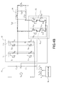
- Fig. 4A and Fig. 4B are circuit diagrams of the DC-to-AC power conversion system under a positive half-cycle energy-storing operation and a positive half-cycle energy-releasing operation, respectively, according to the first embodiment of the present disclosure.
- Fig. 3 is a waveform graph of switch control signals according to a first embodiment of the present disclosure.
- control circuit 15 produces the complementary level signal pair Sc6, Sc7 and Sc5, Sc8 to turn on the sixth power switch S16 and the seventh power switch S17 at high level and turn off the fifth power switch S15 and the eighth power switch S18 at low level.
- the control circuit 15 produces the complementary level signal pair Sc6, Sc7 and Sc5, Sc8 to turn on the sixth power switch S16 and the seventh power switch S17 at high level and turn off the fifth power switch S15 and the eighth power switch S18 at low level.
- the control circuit 15 produces the complementary level signal pair Sc6, Sc7 and Sc5, Sc8 to turn on the sixth power switch S16 and the seventh power switch S17 at high level and turn off the fifth power switch S15 and the eighth power switch S18 at low level.
- the first filter inductor L11 and the second filter inductor L12 are under the energy-storing operation through an energy-storing loop Lps1 sequentially formed by the DC input voltage Vdc, the first power switch S11, the first filter inductor L11, the AC output voltage Vac, the second filter inductor
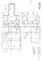
- Fig. 5A and Fig. 5B are circuit diagrams of the DC-to-AC power conversion system under a negative half-cycle energy-storing operation and a negative half-cycle energy-releasing operation, respectively, according to the first embodiment of the present disclosure.
- the control circuit 15 produces the complementary switching signal pair Sc2, Sc3 and Sc1, Sc4 to switch the second power switch S12 and the third power switch S13 and turn off the first power switch S11 and the fourth power switch S14 at low level.
- control circuit 15 produces the complementary level signal pair Sc5, Sc8 and Sc6, Sc7 to turn on the fifth power switch S15 and the eighth power switch S18 at high level and turn off the sixth power switch S16 and the seventh power switch S17 at low level.
- the control circuit 15 produces the complementary level signal pair Sc5, Sc8 and Sc6, Sc7 to turn on the fifth power switch S15 and the eighth power switch S18 at high level and turn off the sixth power switch S16 and the seventh power switch S17 at low level.
- the control circuit 15 produces the complementary level signal pair Sc5, Sc8 and Sc6, Sc7 to turn on the fifth power switch S15 and the eighth power switch S18 at high level and turn off the sixth power switch S16 and the seventh power switch S17 at low level.
- Fig. 6 is a circuit diagram of a DC-to-AC power conversion system according to a second embodiment of the present disclosure.
- the DC-to-AC power conversion system is provided to convert a DC input voltage Vdc into an AC output voltage Vac.
- the DC-to-AC power conversion system includes an input capacitor set 21, a first bridge switching circuit 221, a first auxiliary switch circuit 231, a second bridge switching circuit 222, a second auxiliary switch circuit 232, a first filter circuit 241, a second filter circuit 242, and a control circuit 25.
- the input capacitor set 21 receives the DC input voltage Vdc.
- the input capacitor set 21 has a first capacitor C21 and a second capacitor C22.
- the first capacitor C21 and the second capacitor C22 are connected to a neutral point Po to maintain a voltage across the first capacitor C11 and a voltage across the second capacitor C12 are equal to a half of the DC input voltage Vdc.
- the first bridge switching circuit 221 is connected in parallel to the input capacitor set 21.
- the first bridge switching circuit 221 has a first bridge arm L211 and a second bridge arm L221 connected in parallel to the first bridge arm L211.
- the first bridge arm L211 is composed of a first power switch S211 and a fifth diode D251 connected in series to the first power switch S211.
- the second bridge arm L221 is composed of a second power switch S221 and a sixth diode D261 connected in series to the second power switch S221.
- the first auxiliary switch circuit 231 is connected between the neutral point Po and the first bridge switching circuit 221.
- the first auxiliary switch circuit 231 has a third bridge arm L231 and a fourth bridge arm L241 connected in parallel to the third bridge arm L231.
- the third bridge arm L231 is composed of a third power switch S231 and a seventh diode D271 connected in series to the third power switch S231.
- the fourth bridge arm L241 is composed of a fourth power switch S241 and an eighth diode D281 connected in series to the fourth power switch S241.
- the second bridge switching circuit 222 is connected in parallel to the input capacitor set 21.
- the second bridge switching circuit 222 has a first bridge arm L212 and a second bridge arm L222 connected in parallel to the first bridge arm L212.
- the first bridge arm L212 is composed of a first power switch S212 and a fifth diode D252 connected in series to the first power switch S212.
- the second bridge arm L222 is composed of a second power switch S222 and a sixth diode D262 connected in series to the second power switch S222.
- the second auxiliary switch circuit 232 is connected between the neutral point Po and the second bridge switching circuit 222.
- the second auxiliary switch circuit 232 has a third bridge arm L232 and a fourth bridge arm L242 connected in parallel to the third bridge arm L232.
- the third bridge arm L232 is composed of a third power switch S232 and a seventh diode D272 connected in series to the third power switch S232.
- the fourth bridge arm L242 is composed of a fourth power switch S242 and an eighth diode D282 connected in series to the fourth power switch S242.
- the first filter circuit 241 is connected to the first bridge switching circuit 221 and the first auxiliary switch circuit 231.
- the first filter circuit 241 has a first filter inductor L211, a second filter inductor L221, and a filter capacitor C20.
- the second filter circuit 242 is connected to the second bridge switching circuit 222 and the second auxiliary switch circuit 232.
- the second filter circuit 242 has a first filter inductor L212, a second filter inductor L222, and the filter capacitor C20.
- the control circuit 25 produces a complementary switching signal pair Sc11, Sc21 and Sc12, Sc22 and a complementary level signal pair Sc31, Sc41 and Sc32, Sc42.
- the complementary switching signal pair Sc11, Sc21 and Sc12, Sc22 is provided to control the first and second power switches S211, S221 of the first bridge switching circuit 221 and the first and second power switches S212, S222 of the second bridge switching circuit 222, respectively.
- the complementary level signal pair Sc31, Sc41 and Sc32, Sc42 is provided to control the third and fourth power switches S231, S241 of the first auxiliary switch circuit 231 and the third and fourth power switches S232, S242 of the second auxiliary switch circuit 232, respectively.
- the first power switch S211 and the second power switch S221 of the first bridge switching circuit 221 are connected in parallel to a diode, respectively, namely, a first diode D211 and a second diode D221.
- the third power switch S231 and the fourth power switch S241 of the first auxiliary switch circuit 231 are connected in parallel to a diode, respectively, namely, a third diode D231 and a fourth diode D241.
- the first power switch S212 and the second power switch S222 of the second bridge switching circuit 222 are connected in parallel to a diode, respectively, namely, a first diode D212 and a second diode D222.
- the third power switch S232 and the fourth power switch S242 of the second auxiliary switch circuit 232 are connected in parallel to a diode, respectively, namely, a third diode D232 and a fourth diode D242.
- Fig. 8A and Fig. 8B are circuit diagrams of the DC-to-AC power conversion system under a positive half-cycle energy-storing operation and a positive half-cycle energy-releasing operation, respectively, according to the second embodiment of the present disclosure.
- Fig. 7 is a waveform graph of switch control signals according to a second embodiment of the present disclosure.
- the control circuit 25 When the AC output voltage Vac is under the positive half-cycle operation (during a time interval between time t0 and time t1), the control circuit 25 produces the complementary switching signal pair Sc11, Sc21 and Sc12, Sc22 to switch the first power switch S211 and the second power switch S221 of the first bridge switching circuit 221 and turn off the first power switch S212 and the second power switch S222 of the second bridge switching circuit 222 at low level. Also, the control circuit 25 produces the complementary level signal pair Sc31, Sc41 and Sc32, Sc42 to turn on the third power switch S231 and the fourth power switch S241 of the first auxiliary switch circuit 231 at high level and turn off the third power switch S232 and the fourth power switch S242 of the second auxiliary switch circuit 232 at low level.
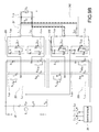
- Fig. 9A and Fig. 9B are circuit diagrams of the DC-to-AC power conversion system under a negative half-cycle energy-storing operation and a negative half-cycle energy-releasing operation, respectively, according to the second embodiment of the present disclosure.
- the control circuit 25 produces the complementary switching signal pair Sc12, Sc22 and Sc11, Sc21 to switch the first power switch S212 and the second power switch S222 of the second bridge switching circuit 222 and turn off the first power switch S211 and the second power switch S221 of the first bridge switching circuit 221 at low level.
- control circuit 25 produces the complementary level signal pair Sc32, Sc42 and Sc31, Sc41 to turn on the third power switch S232 and the fourth power switch S242 of the second auxiliary switch circuit 232 at high level and turn off the third power switch S231 and the fourth power switch S241 of the first auxiliary switch circuit 231 at low level.
- Fig. 9A when the first filter inductor L212 and the second filter inductor L222 are under the energy-storing operation through an energy-storing loop Lns2 sequentially formed by the DC input voltage Vdc, the first power switch S212, the first filter inductor L212, the AC output voltage Vac, the second filter inductor L222, the second power switch S222, and the DC input voltage Vdc.
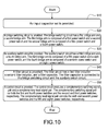
- Fig. 10 is a flowchart of a method of operating a DC-to-AC power conversion system according to the present disclosure.
- the DC-to-AC power conversion system converts a DC input voltage into an AC output voltage and the method includes following steps.
- an input capacitor set is provided (S10).
- the input capacitor set has a first capacitor and a second capacitor, and the first capacitor and the second capacitor are connected to a neutral point and configured to receive the DC input voltage so as to maintain a voltage across the first capacitor and a voltage across the second capacitor are equal to a half of the DC input voltage.
- a bridge switching circuit is provided (S20).
- the bridge switching circuit is connected in parallel to the input capacitor set, and the bridge switching circuit has a first bridge arm and a second bridge arm connected in parallel to the first bridge arm.
- the first bridge arm is composed of a first power switch and a second power switch connected in series to the first power switch
- the second bridge arm is composed of a third power switch and a fourth power switch connected in series to the third power switch.
- the first power switch, the second power switch, the third power switch, and the fourth power switch of the bridge switching circuit are connected in parallel to a diode, respectively, namely, a first diode, a second diode, a third diode, and a fourth diode.
- an auxiliary switch circuit is provided (S30).
- the auxiliary switch circuit is connected between the neutral point and the bridge switching circuit, and the auxiliary switch circuit has a third bridge arm and a fourth bridge arm connected in parallel to the third bridge arm.
- the third bridge arm is composed of a fifth power switch and a sixth power switch connected in series to the fifth power switch
- the fourth bridge arm is composed of a seventh power switch and an eighth power switch connected in series to the seventh power switch.
- the fifth power switch, the sixth power switch, the seventh power switch, and the eighth power switch of the auxiliary switch circuit are connected in parallel to a diode, respectively, namely, a fifth diode, a sixth diode, a seventh diode, and an eighth diode.
- a filter circuit is provided (S40).
- the filter circuit has a first filter inductor, a second filter inductor, and a filter capacitor.
- the filter capacitor is connected between the first filter inductor and the second filter inductor, the first filter inductor is connected to the first bridge arm and the third bridge arm, and the second filter inductor is connected to the second bridge arm and the fourth bridge arm.
- a control circuit is provided (S50).
- the control circuit is configured to produce a complementary switching signal pair and a complementary level signal pair.
- the complementary switching signal pair is configured to control the first and fourth power switches and the second and third power switches, respectively.
- the complementary level signal pair is configured to control the sixth and seventh power switches and the fifth and eighth power switches, respectively.
- the control circuit When the AC output voltage is under the positive half-cycle operation, the control circuit is configured to produce the complementary switching signal pair to switch the first power switch and the fourth power switch and turn off the second power switch and the third power switch at low level.
- the control circuit is configured to produce the complementary level signal pair to turn on the sixth power switch and the seventh power switch at high level and turn off the fifth power switch and the eighth power switch at low level.
- an energy-storing loop is sequentially formed by the DC input voltage, the first power switch, the first filter inductor, the AC output voltage, the second filter inductor, the fourth power switch, and the DC input voltage.
- the control circuit When the AC output voltage is under the positive half-cycle operation, the control circuit is configured to produce the complementary switching signal pair to switch the first power switch and the fourth power switch and turn off the second power switch and the third power switch at low level.
- the control circuit is configured to produce the complementary level signal pair to turn on the sixth power switch and the seventh power switch at high level and turn off the fifth power switch and the eighth power switch at low level.
- an energy-releasing loop is sequentially formed by the first filter inductor, the AC output voltage, the second filter inductor, the seventh power switch, the eighth diode, the sixth power switch, the fifth diode, and the first filter inductor.
- the control circuit When the AC output voltage is under the negative half-cycle operation, the control circuit is configured to produce the complementary switching signal pair to switch the second power switch and the third power switch and turn off the first power switch and the fourth power switch at low level.
- the control circuit is configured to produce the complementary level signal pair to turn on the fifth power switch and the eighth power switch at high level and turn off the sixth power switch and the seventh power switch at low level.
- an energy-storing loop is sequentially formed by the DC input voltage, the third power switch, the second filter inductor, the AC output voltage, the first filter inductor, the second power switch, and the DC input voltage.
- the control circuit When the AC output voltage is under the negative half-cycle operation, the control circuit is configured to produce the complementary switching signal pair to switch the second power switch and the third power switch and turn off the first power switch and the fourth power switch at low level.
- the control circuit is configured to produce the complementary level signal pair to turn on the fifth power switch and the eighth power switch at high level and turn off the sixth power switch and the seventh power switch at low level.
- an energy-releasing loop is sequentially formed by the second filter inductor, the AC output voltage, the first filter inductor, the fifth power switch, the sixth diode, the eighth power switch, the seventh diode, and the second filter inductor.
Landscapes
- Engineering & Computer Science (AREA)
- Power Engineering (AREA)
- Inverter Devices (AREA)
- Rectifiers (AREA)
Abstract
Description
- The present disclosure relates generally to a DC-to-AC power conversion system and a method of operating the same, and more particularly to a DC-to-AC power conversion system and a method of operating the same which are provided to reduce leakage currents caused by parasitic capacitance voltages.
- Reference is made to
Fig. 1 which is a circuit diagram of a prior art full-bridge inverter. Under the zero voltage condition, the full-bridge inverter is provided to decouple the DC side and the AC side. In theory, under the zero voltage condition, the voltage between point A and point N (referred to as "VAN" hereinafter) and the voltage between point B and point N (referred to as "VBN" hereinafter are a half of the DC voltage Vdc, namely, VAN=VBN=1/2Vdc. Hence, the common mode voltage of the point A and the point B is fixed to reduce leakage currents Icp1, Icp2 caused by parasitic capacitance voltages. However, the leakage current Icp1, Icp2 would be rapidly changed once the parasitic capacitance voltages of the parasitic capacitances Cp1, Cp2 significantly change because the zero voltage conditions occur under the exchanging phase of the AC source. That is, the leakage currents get larger as the variation of the parasitic capacitance voltages gets larger. In fact, the voltage VAN and the voltage VBN are not exactly equal to a half of the DC voltage Vdc because the characteristics of circuit components and the parasitic capacitances Cp1, Cp2 are not identical, so that the common mode voltage of the point A and the point B is not fixed. - Accordingly, it is desirable to provide a DC-to-AC power conversion system and a method of operating the same so that an auxiliary switch circuit is used to provide energy-releasing loops. Also, the auxiliary switch circuit is connected to the neutral point to significantly reduce leakage currents caused by parasitic capacitance voltages.
- An object of the present disclosure is to provide a DC-to-AC power conversion system to solve the above-mentioned problems. Accordingly, the DC-to-AC power conversion system is provided to convert a DC input voltage into an AC output voltage. The DC-to-AC power conversion system includes an input capacitor set, a bridge switching circuit, an auxiliary switch circuit, a filter circuit, and a control circuit. The input capacitor set has a first capacitor and a second capacitor. The first capacitor and the second capacitor are connected to a neutral point and configured to receive the DC input voltage. The bridge switching circuit is connected in parallel to the input capacitor set. The bridge switching circuit has a first bridge arm and a second bridge arm connected in parallel to the first bridge arm. The first bridge arm is composed of a first power switch and a second power switch connected in series to the first power switch. The second bridge arm is composed of a third power switch and a fourth power switch connected in series to the third power switch. The auxiliary switch circuit is connected between the neutral point and the bridge switching circuit. The auxiliary switch circuit has a third bridge arm and a fourth bridge arm connected in parallel to the third bridge arm. The third bridge arm is composed of a fifth power switch and a sixth power switch connected in series to the fifth power switch. The fourth bridge arm is composed of a seventh power switch and an eighth power switch connected in series to the seventh power switch. The filter circuit has a first filter inductor, a second filter inductor, and a filter capacitor. The filter capacitor is connected between the first filter inductor and the second filter inductor. The first filter inductor is connected to the first bridge arm and the third bridge arm, and the second filter inductor is connected to the second bridge arm and the fourth bridge arm. The control circuit produces a complementary switching signal pair and a complementary level signal pair. The complementary switching signal pair is configured to control the first and fourth power switches and the second and third power switches, respectively. The complementary level signal pair is configured to control the sixth and seventh power switches and the fifth and eighth power switches, respectively. In particular, the auxiliary switch circuit is configured to provide the energy-releasing loops of the first filter inductor and the second filter inductor to reduce leakage currents of the DC input voltage caused by parasitic capacitance voltages.
- Another object of the present disclosure is to provide a method of operating a DC-to-AC power conversion system to solve the above-mentioned problems. Accordingly, the method includes following steps: (a) providing an input capacitor set, the input capacitor set having a first capacitor and a second capacitor, and the first capacitor and the second capacitor connected to a neutral point and configured to receive the DC input voltage; (b) providing a bridge switching circuit, the bridge switching circuit connected in parallel to the input capacitor set, and the bridge switching circuit having a first bridge arm and a second bridge arm connected in parallel to the first bridge arm; wherein the first bridge arm is composed of a first power switch and a second power switch connected in series to the first power switch, and the second bridge arm is composed of a third power switch and a fourth power switch connected in series to the third power switch; (c) providing an auxiliary switch circuit, the auxiliary switch circuit connected between the neutral point and the bridge switching circuit, and the auxiliary switch circuit having a third bridge arm and a fourth bridge arm connected in parallel to the third bridge arm; wherein the third bridge arm is composed of a fifth power switch and a sixth power switch connected in series to the fifth power switch, and the fourth bridge arm is composed of a seventh power switch and an eighth power switch connected in series to the seventh power switch; (d) providing a filter circuit, the filter circuit having a first filter inductor, a second filter inductor, and a filter capacitor; wherein the filter capacitor is connected between the first filter inductor and the second filter inductor, the first filter inductor is connected to the first bridge arm and the third bridge arm, and the second filter inductor is connected to the second bridge arm and the fourth bridge arm; (e) providing a control circuit, the control circuit configured to produce a complementary switching signal pair and a complementary level signal pair; wherein the complementary switching signal pair is configured to control the first and fourth power switches and the second and third power switches, respectively; the complementary level signal pair is configured to control the sixth and seventh power switches and the fifth and eighth power switches, respectively.
- It is to be understood that both the foregoing general description and the following detailed description are exemplary, and are intended to provide further explanation of the present disclosure as claimed. Other advantages and features of the present disclosure will be apparent from the following description, drawings and claims.
- The features of the present disclosure believed to be novel are set forth with particularity in the appended claims. The present disclosure itself, however, may be best understood by reference to the following detailed description of the present disclosure, which describes an exemplary embodiment of the present disclosure, taken in conjunction with the accompanying drawings, in which:
-
Fig. 1 is a circuit diagram of a prior art full-bridge inverter; -
Fig. 2 is a circuit diagram of a DC-to-AC power conversion system according to a first embodiment of the present disclosure; -
Fig. 3 is a waveform graph of switch control signals according to a first embodiment of the present disclosure; -
Fig. 4A is a circuit diagram of the DC-to-AC power conversion system under a positive half-cycle and energy-storing operation according to the first embodiment of the present disclosure; -
Fig. 4B is a circuit diagram of the DC-to-AC power conversion system under a positive half-cycle and energy-releasing operation according to the first embodiment of the present disclosure; -
Fig. 5A is a circuit diagram of the DC-to-AC power conversion system under a negative half-cycle and energy-storing operation according to the first embodiment of the present disclosure; -
Fig. 5B is a circuit diagram of the DC-to-AC power conversion system under a negative half-cycle and energy-releasing operation according to the first embodiment of the present disclosure; -
Fig. 6 is a circuit diagram of a DC-to-AC power conversion system according to a second embodiment of the present disclosure; -
Fig. 7 is a waveform graph of switch control signals according to a second embodiment of the present disclosure; -
Fig. 8A is a circuit diagram of the DC-to-AC power conversion system under a positive half-cycle and energy-storing operation according to the second embodiment of the present disclosure; -
Fig. 8B is a circuit diagram of the DC-to-AC power conversion system under a positive half-cycle and energy-releasing operation according to the second embodiment of the present disclosure; -
Fig. 9A is a circuit diagram of the DC-to-AC power conversion system under a negative half-cycle and energy-storing operation according to the second embodiment of the present disclosure; -
Fig. 9B is a circuit diagram of the DC-to-AC power conversion system under a negative half-cycle and energy-releasing operation according to the second embodiment of the present disclosure; and -
Fig. 10 is a flowchart of a method of operating a DC-to-AC power conversion system according to the present disclosure. - Reference will now be made to the drawing figures to describe the present disclosure in detail.
- Reference is made to
Fig. 2 which is a circuit diagram of a DC-to-AC power conversion system according to a first embodiment of the present disclosure. The DC-to-AC power conversion system is provided to convert a DC input voltage Vdc into an AC output voltage Vac. The DC-to-AC power conversion system includes an input capacitor set 11, abridge switching circuit 12, anauxiliary switch circuit 13, afilter circuit 14, and acontrol circuit 15. The input capacitor set 11 receives the DC input voltage Vdc. The input capacitor set 11 has a first capacitor C11 and a second capacitor C12. The first capacitor C11 and the second capacitor C12 are connected to a neutral point Po to maintain a voltage across the first capacitor C11 and a voltage across the second capacitor C12 are equal to a half of the DC input voltage Vdc. Thebridge switching circuit 12 is connected in parallel to the input capacitor set 11. Thebridge switching circuit 12 has a first bridge arm L11 and a second bridge arm L12 connected in parallel to the first bridge arm L11. The first bridge arm L11 is composed of a first power switch S11 and a second power switch S12 connected in series to the first power switch S11. The second bridge arm L12 is composed of a third power switch S13 and a fourth power switch S14 connected in series to the third power switch S13. In this embodiment, thebridge switching circuit 12 is a full-bridge switching circuit. Theauxiliary switch circuit 13 is connected between the neutral point Po and thebridge switching circuit 12. Theauxiliary switch circuit 13 has a third bridge arm L13 and a fourth bridge arm L14 connected in parallel to the third bridge arm L13. The third bridge arm L13 is composed of a fifth power switch S15 and a sixth power switch S16 connected in series to the fifth power switch S15. The fourth bridge arm L14 is composed of a seventh power switch S17 and an eighth power switch S18 connected in series to the seventh power switch S17. - The
filter circuit 14 is connected to thebridge switching circuit 12 and theauxiliary switch circuit 13. Thefilter circuit 14 has a first filter inductor L11, a second filter inductor L12, and a filter capacitor C10. The filter capacitor C10 is connected between the first filter inductor L11 and the second filter inductor L12. The first filter inductor L11 is connected to the first bridge arm L11 and the third bridge arm L13, and the second filter inductor L12 is connected to the second bridge arm L12 and the fourth bridge arm L14. Thecontrol circuit 15 produces a complementary switching signal pair Sc1, Sc4 and Sc2, Sc3 and a complementary level signal pair Sc6, Sc7 and Sc5, Sc8. The complementary switching signal pair Sc1, Sc4 and Sc2, Sc3 is provided to control the first and fourth power switches S11, S14 and the second and third power switches S12, S13, respectively. The complementary level signal pair Sc6, Sc7 and Sc5, Sc8 is provided to control the sixth and seventh power switches S16, S17 and the fifth and eighth power switches S15, S18, respectively. In addition, the first power switch S11, the second power switch S12, the third power switch S13, and the fourth power switch S14 of thebridge switching circuit 12 are connected in parallel to a diode, respectively, namely, a first diode D11, a second diode D12, a third diode D13, and a fourth diode D14. The fifth power switch S15, the sixth power switch S16, the seventh power switch S17, and the eighth power switch S18 of theauxiliary switch circuit 13 are connected in parallel to a diode, respectively, namely, a fifth diode D15, a sixth diode D16, a seventh diode D17, and an eighth diode D18. The detailed operation of the DC-to-AC power conversion system will be described hereinafter as follows. - Reference is made to
Fig. 4A andFig. 4B which are circuit diagrams of the DC-to-AC power conversion system under a positive half-cycle energy-storing operation and a positive half-cycle energy-releasing operation, respectively, according to the first embodiment of the present disclosure. In addition, reference is made toFig. 3 which is a waveform graph of switch control signals according to a first embodiment of the present disclosure. When the AC output voltage Vac is under the positive half-cycle operation (during a time interval between time t0 and time t1), thecontrol circuit 15 produces the complementary switching signal pair Sc1, Sc4 and Sc2, Sc3 to switch the first power switch S11 and the fourth power switch S14 and turn off the second power switch S12 and the third power switch S13 at low level. Also, thecontrol circuit 15 produces the complementary level signal pair Sc6, Sc7 and Sc5, Sc8 to turn on the sixth power switch S16 and the seventh power switch S17 at high level and turn off the fifth power switch S15 and the eighth power switch S18 at low level. As shown inFig. 4A , when the first filter inductor L11 and the second filter inductor L12 are under the energy-storing operation through an energy-storing loop Lps1 sequentially formed by the DC input voltage Vdc, the first power switch S11, the first filter inductor L11, the AC output voltage Vac, the second filter inductor L12, the fourth power switch S14, and the DC input voltage Vdc. As shown inFig. 4B , when the first filter inductor L11 and the second filter inductor L12 are under the energy-releasing operation through an energy-releasing loop Lpr1 sequentially formed by the first filter inductor L11, the AC output voltage Vac, the second filter inductor L12, the seventh power switch S17, the eighth diode D18, the sixth power switch S16, the fifth diode D15, and the first filter inductor L11. - Reference is made to
Fig. 5A andFig. 5B which are circuit diagrams of the DC-to-AC power conversion system under a negative half-cycle energy-storing operation and a negative half-cycle energy-releasing operation, respectively, according to the first embodiment of the present disclosure. When the AC output voltage Vac is under the negative half-cycle operation (during a time interval between time t1 and time t2), thecontrol circuit 15 produces the complementary switching signal pair Sc2, Sc3 and Sc1, Sc4 to switch the second power switch S12 and the third power switch S13 and turn off the first power switch S11 and the fourth power switch S14 at low level. Also, thecontrol circuit 15 produces the complementary level signal pair Sc5, Sc8 and Sc6, Sc7 to turn on the fifth power switch S15 and the eighth power switch S18 at high level and turn off the sixth power switch S16 and the seventh power switch S17 at low level. As shown inFig. 5A , when the first filter inductor L11 and the second filter inductor L12 are under the energy-storing operation through an energy-storing loop Lns1 sequentially formed by the DC input voltage Vdc, the third power switch S13, the second filter inductor L12, the AC output voltage Vac, the first filter inductor L11, the second power switch S12, and the DC input voltage Vdc. As shown inFig. 5B , when the first filter inductor L11 and the second filter inductor L12 are under the energy-releasing operation through an energy-releasing loop Lnr1 sequentially formed by the second filter inductor L12, the AC output voltage Vac, the first filter inductor L11, the fifth power switch S15, the sixth diode D16, the eighth power switch S18, the seventh diode D17, and the second filter inductor L12. - Reference is made to
Fig. 6 which is a circuit diagram of a DC-to-AC power conversion system according to a second embodiment of the present disclosure. The DC-to-AC power conversion system is provided to convert a DC input voltage Vdc into an AC output voltage Vac. The DC-to-AC power conversion system includes an input capacitor set 21, a firstbridge switching circuit 221, a firstauxiliary switch circuit 231, a secondbridge switching circuit 222, a secondauxiliary switch circuit 232, afirst filter circuit 241, asecond filter circuit 242, and acontrol circuit 25. The input capacitor set 21 receives the DC input voltage Vdc. The input capacitor set 21 has a first capacitor C21 and a second capacitor C22. The first capacitor C21 and the second capacitor C22 are connected to a neutral point Po to maintain a voltage across the first capacitor C11 and a voltage across the second capacitor C12 are equal to a half of the DC input voltage Vdc. The firstbridge switching circuit 221 is connected in parallel to the input capacitor set 21. The firstbridge switching circuit 221 has a first bridge arm L211 and a second bridge arm L221 connected in parallel to the first bridge arm L211. The first bridge arm L211 is composed of a first power switch S211 and a fifth diode D251 connected in series to the first power switch S211. The second bridge arm L221 is composed of a second power switch S221 and a sixth diode D261 connected in series to the second power switch S221. The firstauxiliary switch circuit 231 is connected between the neutral point Po and the firstbridge switching circuit 221. The firstauxiliary switch circuit 231 has a third bridge arm L231 and a fourth bridge arm L241 connected in parallel to the third bridge arm L231. The third bridge arm L231 is composed of a third power switch S231 and a seventh diode D271 connected in series to the third power switch S231. The fourth bridge arm L241 is composed of a fourth power switch S241 and an eighth diode D281 connected in series to the fourth power switch S241. - The second
bridge switching circuit 222 is connected in parallel to the input capacitor set 21. The secondbridge switching circuit 222 has a first bridge arm L212 and a second bridge arm L222 connected in parallel to the first bridge arm L212. The first bridge arm L212 is composed of a first power switch S212 and a fifth diode D252 connected in series to the first power switch S212. The second bridge arm L222 is composed of a second power switch S222 and a sixth diode D262 connected in series to the second power switch S222. The secondauxiliary switch circuit 232 is connected between the neutral point Po and the secondbridge switching circuit 222. The secondauxiliary switch circuit 232 has a third bridge arm L232 and a fourth bridge arm L242 connected in parallel to the third bridge arm L232. The third bridge arm L232 is composed of a third power switch S232 and a seventh diode D272 connected in series to the third power switch S232. The fourth bridge arm L242 is composed of a fourth power switch S242 and an eighth diode D282 connected in series to the fourth power switch S242. - The
first filter circuit 241 is connected to the firstbridge switching circuit 221 and the firstauxiliary switch circuit 231. Thefirst filter circuit 241 has a first filter inductor L211, a second filter inductor L221, and a filter capacitor C20. Thesecond filter circuit 242 is connected to the secondbridge switching circuit 222 and the secondauxiliary switch circuit 232. Thesecond filter circuit 242 has a first filter inductor L212, a second filter inductor L222, and the filter capacitor C20. Thecontrol circuit 25 produces a complementary switching signal pair Sc11, Sc21 and Sc12, Sc22 and a complementary level signal pair Sc31, Sc41 and Sc32, Sc42. The complementary switching signal pair Sc11, Sc21 and Sc12, Sc22 is provided to control the first and second power switches S211, S221 of the firstbridge switching circuit 221 and the first and second power switches S212, S222 of the secondbridge switching circuit 222, respectively. The complementary level signal pair Sc31, Sc41 and Sc32, Sc42 is provided to control the third and fourth power switches S231, S241 of the firstauxiliary switch circuit 231 and the third and fourth power switches S232, S242 of the secondauxiliary switch circuit 232, respectively. In addition, the first power switch S211 and the second power switch S221 of the firstbridge switching circuit 221 are connected in parallel to a diode, respectively, namely, a first diode D211 and a second diode D221. The third power switch S231 and the fourth power switch S241 of the firstauxiliary switch circuit 231 are connected in parallel to a diode, respectively, namely, a third diode D231 and a fourth diode D241. The first power switch S212 and the second power switch S222 of the secondbridge switching circuit 222 are connected in parallel to a diode, respectively, namely, a first diode D212 and a second diode D222. The third power switch S232 and the fourth power switch S242 of the secondauxiliary switch circuit 232 are connected in parallel to a diode, respectively, namely, a third diode D232 and a fourth diode D242. The detailed operation of the DC-to-AC power conversion system will be described hereinafter as follows. - Reference is made to
Fig. 8A andFig. 8B which are circuit diagrams of the DC-to-AC power conversion system under a positive half-cycle energy-storing operation and a positive half-cycle energy-releasing operation, respectively, according to the second embodiment of the present disclosure. In addition, reference is made toFig. 7 which is a waveform graph of switch control signals according to a second embodiment of the present disclosure. When the AC output voltage Vac is under the positive half-cycle operation (during a time interval between time t0 and time t1), thecontrol circuit 25 produces the complementary switching signal pair Sc11, Sc21 and Sc12, Sc22 to switch the first power switch S211 and the second power switch S221 of the firstbridge switching circuit 221 and turn off the first power switch S212 and the second power switch S222 of the secondbridge switching circuit 222 at low level. Also, thecontrol circuit 25 produces the complementary level signal pair Sc31, Sc41 and Sc32, Sc42 to turn on the third power switch S231 and the fourth power switch S241 of the firstauxiliary switch circuit 231 at high level and turn off the third power switch S232 and the fourth power switch S242 of the secondauxiliary switch circuit 232 at low level. As shown inFig. 8A , when the first filter inductor L211 and the second filter inductor L221 are under the energy-storing operation through an energy-storing loop Lps2 sequentially formed by the DC input voltage Vdc, the first power switch S211, the first filter inductor L211, the AC output voltage Vac, the second filter inductor L221, the second power switch S221, and the DC input voltage Vdc. As shown inFig. 8B , when the first filter inductor L211 and the second filter inductor L221 are under the energy-releasing operation through an energy-releasing loop Lpr2 sequentially formed by the first filter inductor L211, the AC output voltage Vac, the second filter inductor L221, the fourth power switch S241, the eighth diode D281, the third power switch S231, the seventh diode D271, and the first filter inductor L211. - Reference is made to
Fig. 9A andFig. 9B which are circuit diagrams of the DC-to-AC power conversion system under a negative half-cycle energy-storing operation and a negative half-cycle energy-releasing operation, respectively, according to the second embodiment of the present disclosure. When the AC output voltage Vac is under the negative half-cycle operation (during a time interval between time t1 and time t2), thecontrol circuit 25 produces the complementary switching signal pair Sc12, Sc22 and Sc11, Sc21 to switch the first power switch S212 and the second power switch S222 of the secondbridge switching circuit 222 and turn off the first power switch S211 and the second power switch S221 of the firstbridge switching circuit 221 at low level. Also, thecontrol circuit 25 produces the complementary level signal pair Sc32, Sc42 and Sc31, Sc41 to turn on the third power switch S232 and the fourth power switch S242 of the secondauxiliary switch circuit 232 at high level and turn off the third power switch S231 and the fourth power switch S241 of the firstauxiliary switch circuit 231 at low level. As shown inFig. 9A , when the first filter inductor L212 and the second filter inductor L222 are under the energy-storing operation through an energy-storing loop Lns2 sequentially formed by the DC input voltage Vdc, the first power switch S212, the first filter inductor L212, the AC output voltage Vac, the second filter inductor L222, the second power switch S222, and the DC input voltage Vdc. As shown inFig. 9B , when the first filter inductor L212 and the second filter inductor L222 are under the energy-releasing operation through an energy-releasing loop Lnr2 sequentially formed by the first filter inductor L212, the AC output voltage Vac, the second filter inductor L222, the fourth power switch S242, the eighth diode D282, the third power switch S232, the seventh diode D272, and the first filter inductor L212. - Reference is made to
Fig. 10 which is a flowchart of a method of operating a DC-to-AC power conversion system according to the present disclosure. The DC-to-AC power conversion system converts a DC input voltage into an AC output voltage and the method includes following steps. First, an input capacitor set is provided (S10). The input capacitor set has a first capacitor and a second capacitor, and the first capacitor and the second capacitor are connected to a neutral point and configured to receive the DC input voltage so as to maintain a voltage across the first capacitor and a voltage across the second capacitor are equal to a half of the DC input voltage. Afterward, a bridge switching circuit is provided (S20). The bridge switching circuit is connected in parallel to the input capacitor set, and the bridge switching circuit has a first bridge arm and a second bridge arm connected in parallel to the first bridge arm. The first bridge arm is composed of a first power switch and a second power switch connected in series to the first power switch, and the second bridge arm is composed of a third power switch and a fourth power switch connected in series to the third power switch. In particular, the first power switch, the second power switch, the third power switch, and the fourth power switch of the bridge switching circuit are connected in parallel to a diode, respectively, namely, a first diode, a second diode, a third diode, and a fourth diode. - Afterward, an auxiliary switch circuit is provided (S30). The auxiliary switch circuit is connected between the neutral point and the bridge switching circuit, and the auxiliary switch circuit has a third bridge arm and a fourth bridge arm connected in parallel to the third bridge arm. The third bridge arm is composed of a fifth power switch and a sixth power switch connected in series to the fifth power switch, and the fourth bridge arm is composed of a seventh power switch and an eighth power switch connected in series to the seventh power switch. In particular, the fifth power switch, the sixth power switch, the seventh power switch, and the eighth power switch of the auxiliary switch circuit are connected in parallel to a diode, respectively, namely, a fifth diode, a sixth diode, a seventh diode, and an eighth diode. Afterward, a filter circuit is provided (S40). The filter circuit has a first filter inductor, a second filter inductor, and a filter capacitor. The filter capacitor is connected between the first filter inductor and the second filter inductor, the first filter inductor is connected to the first bridge arm and the third bridge arm, and the second filter inductor is connected to the second bridge arm and the fourth bridge arm. Afterward, a control circuit is provided (S50). The control circuit is configured to produce a complementary switching signal pair and a complementary level signal pair. The complementary switching signal pair is configured to control the first and fourth power switches and the second and third power switches, respectively. The complementary level signal pair is configured to control the sixth and seventh power switches and the fifth and eighth power switches, respectively.
- When the AC output voltage is under the positive half-cycle operation, the control circuit is configured to produce the complementary switching signal pair to switch the first power switch and the fourth power switch and turn off the second power switch and the third power switch at low level. The control circuit is configured to produce the complementary level signal pair to turn on the sixth power switch and the seventh power switch at high level and turn off the fifth power switch and the eighth power switch at low level. When the first filter inductor and the second filter inductor are under the energy-storing operation, an energy-storing loop is sequentially formed by the DC input voltage, the first power switch, the first filter inductor, the AC output voltage, the second filter inductor, the fourth power switch, and the DC input voltage.
- When the AC output voltage is under the positive half-cycle operation, the control circuit is configured to produce the complementary switching signal pair to switch the first power switch and the fourth power switch and turn off the second power switch and the third power switch at low level. The control circuit is configured to produce the complementary level signal pair to turn on the sixth power switch and the seventh power switch at high level and turn off the fifth power switch and the eighth power switch at low level. When the first filter inductor and the second filter inductor are under the energy-releasing operation, an energy-releasing loop is sequentially formed by the first filter inductor, the AC output voltage, the second filter inductor, the seventh power switch, the eighth diode, the sixth power switch, the fifth diode, and the first filter inductor.
- When the AC output voltage is under the negative half-cycle operation, the control circuit is configured to produce the complementary switching signal pair to switch the second power switch and the third power switch and turn off the first power switch and the fourth power switch at low level. The control circuit is configured to produce the complementary level signal pair to turn on the fifth power switch and the eighth power switch at high level and turn off the sixth power switch and the seventh power switch at low level. When the first filter inductor and the second filter inductor are under the energy-storing operation, an energy-storing loop is sequentially formed by the DC input voltage, the third power switch, the second filter inductor, the AC output voltage, the first filter inductor, the second power switch, and the DC input voltage.
- When the AC output voltage is under the negative half-cycle operation, the control circuit is configured to produce the complementary switching signal pair to switch the second power switch and the third power switch and turn off the first power switch and the fourth power switch at low level. The control circuit is configured to produce the complementary level signal pair to turn on the fifth power switch and the eighth power switch at high level and turn off the sixth power switch and the seventh power switch at low level. When the first filter inductor and the second filter inductor are under the energy-releasing operation, an energy-releasing loop is sequentially formed by the second filter inductor, the AC output voltage, the first filter inductor, the fifth power switch, the sixth diode, the eighth power switch, the seventh diode, and the second filter inductor.
- In conclusion, the present disclosure has following advantages:
- 1. The auxiliary switch circuit is used to provide the energy-releasing loops. Also, the auxiliary switch circuit is connected to the neutral point so that the first capacitor and the second capacitor are used to limit the VAN and VBN are equal to a half of the DC input voltage under the zero voltage condition. Accordingly, the common mode voltage of the point A and the point B is fixed to significantly reduce leakage currents caused by parasitic capacitance voltages.
Claims (13)
- A DC-to-AC power conversion system converting a DC input voltage (Vdc) into an AC output voltage (Vac), the DC-to-AC power conversion system comprising:an input capacitor set (11) having a first capacitor (C11) and a second capacitor (C12), and the first capacitor (C11) and the second capacitor (C12) connected to a neutral point (Po) and configured to receive the DC input voltage (Vdc);a bridge switching circuit (12) connected in parallel to the input capacitor set, and the bridge switching circuit (12) having a first bridge arm (L11) and a second bridge arm (L12) connected in parallel to the first bridge arm (L11); wherein the first bridge arm (L11) is composed of a first power switch (S11) and a second power switch (S12) connected in series to the first power switch (S11), and the second bridge arm (L12) is composed of a third power switch (S13) and a fourth power switch (S14) connected in series to the third power switch (S13);an auxiliary switch circuit (13) connected between the neutral point (Po) and the bridge switching circuit (12), and the auxiliary switch circuit (13) having a third bridge arm (L13) and a fourth bridge arm (L14) connected in parallel to the third bridge arm (L13); wherein the third bridge arm (L13) is composed of a fifth power switch (S15) and a sixth power switch (S16) connected in series to the fifth power switch (S15), and the fourth bridge arm (L14) is composed of a seventh power switch (S17) and an eighth power switch (S18) connected in series to the seventh power switch (S17);a filter circuit (14) having a first filter inductor (L11), a second filter inductor (L12), and a filter capacitor (C10); wherein the filter capacitor (C10) is connected between the first filter inductor (L11) and the second filter inductor (L12), the first filter inductor (L11) is connected to the first bridge arm (L11) and the third bridge arm (L13), and the second filter inductor (L12) is connected to the second bridge arm (L12) and the fourth bridge arm (L14); anda control circuit (15) configured to produce a complementary switching signal pair (Sc1, Sc4 and Sc2, Sc3) and a complementary level signal pair (Sc6, Sc7 and Sc5, Sc8); wherein the complementary switching signal pair (Sc1, Sc4 and Sc2, Sc3) is configured to control the first and fourth power switches (S11, S14) and the second and third power switches (S12, S13), respectively; the complementary level signal pair (Sc6, Sc7 and Sc5, Sc8) is configured to control the sixth and seventh power switches (S16, S17) and the fifth and eighth power switches (S15, S18), respectively;wherein the auxiliary switch circuit (13) is configured to provide the energy-releasing loops of the first filter inductor (L11) and the second filter inductor (L12) to reduce leakage currents of the DC input voltage (Vdc) caused by parasitic capacitance voltages.
- The DC-to-AC power conversion system in claim 1, wherein the first power switch (S11), the second power switch (S12), the third power switch (S13), and the fourth power switch (S14) of the bridge switching circuit (12) are connected in parallel to a first diode (D11), a second diode (D12), a third diode (D13), and a fourth diode (D14), respectively; the fifth power switch (S15), the sixth power switch (S16), the seventh power switch (S17), and the eighth power switch (S18) of the auxiliary switch circuit (13) are connected in parallel to a fifth diode (D15), a sixth diode (D16), a seventh diode (D17), and an eighth diode (D18), respectively.
- The DC-to-AC power conversion system in claim 2, wherein when the AC output voltage (Vac) is under the positive half-cycle operation, the control circuit (15) is configured to produce the complementary switching signal pair (Sc1, Sc4 and Sc2, Sc3) to switch the first power switch (S11) and the fourth power switch (S14) and turn off the second power switch (S12) and the third power switch (S13) at low level; and the control circuit (15) is configured to produce the complementary level signal pair (Sc6, Sc7 and Sc5, Sc8) to turn on the sixth power switch (S16) and the seventh power switch (S17) at high level and turn off the fifth power switch (S15) and the eighth power switch (S18) at low level; when the first filter inductor (L11) and the second filter inductor (L12) are under the energy-storing operation, an energy-storing loop (Lps1) is sequentially formed by the DC input voltage (Vdc), the first power switch (S11), the first filter inductor (L11), the AC output voltage (Vac), the second filter inductor (L12), the fourth power switch (S14), and the DC input voltage (Vdc).
- The DC-to-AC power conversion system in claim 2, wherein when the AC output voltage (Vac) is under the positive half-cycle operation, the control circuit (15) is configured to produce the complementary switching signal pair (Sc1, Sc4 and Sc2, Sc3) to switch the first power switch (S11) and the fourth power switch (S14) and turn off the second power switch (S12) and the third power switch (S13) at low level; and the control circuit (15) is configured to produce the complementary level signal pair (Sc6, Sc7 and Sc5, Sc8) to turn on the sixth power switch (S16) and the seventh power switch (S17) at high level and turn off the fifth power switch (S15) and the eighth power switch (S18) at low level; when the first filter inductor (L11) and the second filter inductor (L12) are under the energy-releasing operation, an energy-releasing loop (Lpr1) is sequentially formed by the first filter inductor (L11), the AC output voltage (Vac), the second filter inductor (L12), the seventh power switch (S17), the eighth diode (D18), the sixth power switch (S16), the fifth diode (D15), and the first filter inductor (L11).
- The DC-to-AC power conversion system in claim 2, wherein when the AC output voltage (Vac) is under the negative half-cycle operation, the control circuit (15) is configured to produce the complementary switching signal pair (Sc1, Sc4 and Sc2, Sc3) to switch the second power switch (S12) and the third power switch (S13) and turn off the first power switch (S11) and the fourth power switch (S14) at low level; and the control circuit (15) is configured to produce the complementary level signal pair (Sc6, Sc7 and Sc5, Sc8) to turn on the fifth power switch (S15) and the eighth power switch (S18) at high level and turn off the sixth power switch (S16) and the seventh power switch (S17) at low level; when the first filter inductor (L11) and the second filter inductor (L12) are under the energy-storing operation, an energy-storing loop (Lns1) is sequentially formed by the DC input voltage (Vdc), the third power switch (S13), the second filter inductor (L12), the AC output voltage (Vac), the first filter inductor (L11), the second power switch (S12), and the DC input voltage (Vdc).
- The DC-to-AC power conversion system in claim 2, wherein when the AC output voltage (Vac) is under the negative half-cycle operation, the control circuit (15) is configured to produce the complementary switching signal pair (Sc1, Sc4 and Sc2, Sc3) to switch the second power switch (S12) and the third power switch (S13) and turn off the first power switch (S11) and the fourth power switch (S14) at low level; and the control circuit (15) is configured to produce the complementary level signal pair (Sc6, Sc7 and Sc5, Sc8) to turn on the fifth power switch (S15) and the eighth power switch (S18) at high level and turn off the sixth power switch (S16) and the seventh power switch (S17) at low level; when the first filter inductor (L11) and the second filter inductor (L12) are under the energy-releasing operation, an energy-releasing loop (Lnr1) is sequentially formed by the second filter inductor (L12), the AC output voltage (Vac), the first filter inductor (L11), the fifth power switch (S15), the sixth diode (D16), the eighth power switch (S18), the seventh diode (D17), and the second filter inductor (L12).
- The DC-to-AC power conversion system in claim 1, wherein the first capacitor (C11) and the second capacitor (C12) are connected to a neutral point (Po) to maintain a voltage across the first capacitor (C11) and a voltage across the second capacitor (C12) are equal to a half of the DC input voltage (Vdc).
- A method of operating a DC-to-AC power conversion system, the DC-to-AC power conversion system converting a DC input voltage (Vdc) into an AC output voltage (Vac), the method comprising following steps:(a) providing an input capacitor set (11), the input capacitor set (11) having a first capacitor (C11) and a second capacitor (C12), and the first capacitor (C11) and the second capacitor (C12) connected to a neutral point (Po) and configured to receive the DC input voltage (Vdc) (S10);(b) providing a bridge switching circuit (12), the bridge switching circuit (12) connected in parallel to the input capacitor set (11), and the bridge switching circuit (12) having a first bridge arm (L11) and a second bridge arm (L12) connected in parallel to the first bridge arm (L11); wherein the first bridge arm (L11) is composed of a first power switch (S11) and a second power switch (S12) connected in series to the first power switch (S11), and the second bridge arm (L12) is composed of a third power switch (S13) and a fourth power switch (S14) connected in series to the third power switch (S13) (S20);(c) providing an auxiliary switch circuit (13), the auxiliary switch circuit (13) connected between the neutral point (Po) and the bridge switching circuit (12), and the auxiliary switch circuit (13) having a third bridge arm (L13) and a fourth bridge arm (L14) connected in parallel to the third bridge arm (L13); wherein the third bridge arm (L13) is composed of a fifth power switch (S15) and a sixth power switch (S16) connected in series to the fifth power switch (S15), and the fourth bridge arm (L14) is composed of a seventh power switch (S17) and an eighth power switch (S18) connected in series to the seventh power switch (S17) (S30);(d) providing a filter circuit (14), the filter circuit (14) having a first filter inductor (L11), a second filter inductor (L12), and a filter capacitor (C10); wherein the filter capacitor (C10) is connected between the first filter inductor (L11) and the second filter inductor (L12), the first filter inductor (L11) is connected to the first bridge arm (L11) and the third bridge arm (L13), and the second filter inductor (L12) is connected to the second bridge arm (L12) and the fourth bridge arm (L14) (S40); and(e) providing a control circuit (15), the control circuit (15) configured to produce a complementary switching signal pair (Sc1, Sc4 and Sc2, Sc3) and a complementary level signal pair (Sc6, Sc7 and Sc5, Sc8); wherein the complementary switching signal pair (Sc1, Sc4 and Sc2, Sc3) is configured to control the first and fourth power switches (S11, S14) and the second and third power switches (S12, S13), respectively; the complementary level signal pair (Sc6, Sc7 and Sc5, Sc8) is configured to control the sixth and seventh power switches (S16, S17) and the fifth and eighth power switches (S15, S18), respectively (S50).
- The method of operating the DC-to-AC power conversion system in claim 8, wherein the first power switch (S11), the second power switch (S12), the third power switch (S13), and the fourth power switch (S14) of the bridge switching circuit (12) are connected in parallel to a first diode (D11), a second diode (D12), a third diode (D13), and a fourth diode (D14), respectively; the fifth power switch (S15), the sixth power switch (S16), the seventh power switch (S17), and the eighth power switch (S18) of the auxiliary switch circuit (13) are connected in parallel to a fifth diode (D15), a sixth diode (D16), a seventh diode (D17), and an eighth diode (D18), respectively; wherein the first capacitor (C11) and the second capacitor (C12) are connected to a neutral point (Po) to maintain a voltage across the first capacitor (C11) and a voltage across the second capacitor (C12) are equal to a half of the DC input voltage (Vdc).
- The method of operating the DC-to-AC power conversion system in claim 9, wherein when the AC output voltage (Vac) is under the positive half-cycle operation, the control circuit (15) is configured to produce the complementary switching signal pair (Sc1, Sc4 and Sc2, Sc3) to switch the first power switch (S11) and the fourth power switch (S14) and turn off the second power switch (S12) and the third power switch (S13) at low level; and the control circuit (15) is configured to produce the complementary level signal pair (Sc6, Sc7 and Sc5, Sc8) to turn on the sixth power switch (S16) and the seventh power switch (S17) at high level and turn off the fifth power switch (S15) and the eighth power switch (S18) at low level; when the first filter inductor (L11) and the second filter inductor (L12) are under the energy-storing operation, an energy-storing loop (Lps1) is sequentially formed by the DC input voltage (Vdc), the first power switch (S11), the first filter inductor (L11), the AC output voltage (Vac), the second filter inductor (L12), the fourth power switch (S14), and the DC input voltage (Vdc).
- The method of operating the DC-to-AC power conversion system in claim 9, wherein when the AC output voltage (Vac) is under the positive half-cycle operation, the control circuit (15) is configured to produce the complementary switching signal pair (Sc1, Sc4 and Sc2, Sc3) to switch the first power switch (S11) and the fourth power switch (S14) and turn off the second power switch (S12) and the third power switch (S13) at low level; and the control circuit (15) is configured to produce the complementary level signal pair (Sc6, Sc7 and Sc5, Sc8) to turn on the sixth power switch (S16) and the seventh power switch (S17) at high level and turn off the fifth power switch (S15) and the eighth power switch (S18) at low level; when the first filter inductor (L11) and the second filter inductor (L12) are under the energy-releasing operation, an energy-releasing loop (Lpr1) is sequentially formed by the first filter inductor (L11), the AC output voltage (Vac), the second filter inductor (L12), the seventh power switch (S17), the eighth diode (D18), the sixth power switch (S16), the fifth diode (D15), and the first filter inductor (L11).
- The method of operating the DC-to-AC power conversion system in claim 9, wherein when the AC output voltage (Vac) is under the negative half-cycle operation, the control circuit (15) is configured to produce the complementary switching signal pair (Sc1, Sc4 and Sc2, Sc3) to switch the second power switch (S12) and the third power switch (S13) and turn off the first power switch (S11) and the fourth power switch (S14) at low level; and the control circuit (15) is configured to produce the complementary level signal pair (Sc6, Sc7 and Sc5, Sc8) to turn on the fifth power switch (S15) and the eighth power switch (S18) at high level and turn off the sixth power switch (S16) and the seventh power switch (S17) at low level; when the first filter inductor (L11) and the second filter inductor (L12) are under the energy-storing operation, an energy-storing loop (Lns1) is sequentially formed by the DC input voltage (Vdc), the third power switch (S13), the second filter inductor (L12), the AC output voltage (Vac), the first filter inductor (L11), the second power switch (S12), and the DC input voltage (Vdc).
- The method of operating the DC-to-AC power conversion system in claim 9, wherein when the AC output voltage (Vac) is under the negative half-cycle operation, the control circuit (15) is configured to produce the complementary switching signal pair (Sc1, Sc4 and Sc2, Sc3) to switch the second power switch (S12) and the third power switch (S13) and turn off the first power switch (S11) and the fourth power switch (S14) at low level; and the control circuit (15) is configured to produce the complementary level signal pair (Sc6, Sc7 and Sc5, Sc8) to turn on the fifth power switch (S15) and the eighth power switch (S18) at high level and turn off the sixth power switch (S16) and the seventh power switch (S17) at low level; when the first filter inductor (L11) and the second filter inductor (L12) are under the energy-releasing operation, an energy-releasing loop (Lnr1) is sequentially formed by the second filter inductor (L12), the AC output voltage (Vac), the first filter inductor (L11), the fifth power switch (S15), the sixth diode (D16), the eighth power switch (S18), the seventh diode (D17), and the second filter inductor (L12).
Applications Claiming Priority (1)
| Application Number | Priority Date | Filing Date | Title |
|---|---|---|---|
| TW102112008A TWI488421B (en) | 2013-04-03 | 2013-04-03 | DC to AC power conversion system and operation method thereof |
Publications (3)
| Publication Number | Publication Date |
|---|---|
| EP2787616A2 true EP2787616A2 (en) | 2014-10-08 |
| EP2787616A3 EP2787616A3 (en) | 2015-06-10 |
| EP2787616B1 EP2787616B1 (en) | 2018-01-31 |
Family
ID=48740956
Family Applications (1)
| Application Number | Title | Priority Date | Filing Date |
|---|---|---|---|
| EP13175139.8A Active EP2787616B1 (en) | 2013-04-03 | 2013-07-04 | DC-to-AC power conversion system and method of operating the same |
Country Status (5)
| Country | Link |
|---|---|
| US (1) | US9019736B2 (en) |
| EP (1) | EP2787616B1 (en) |
| JP (1) | JP5736415B2 (en) |
| ES (1) | ES2662424T3 (en) |
| TW (1) | TWI488421B (en) |
Cited By (2)
| Publication number | Priority date | Publication date | Assignee | Title |
|---|---|---|---|---|
| JP2015142504A (en) * | 2014-01-29 | 2015-08-03 | 台達電子工業股▲ふん▼有限公司Delta Electronics,Inc. | Power conversion system and operation method thereof |
| EP3051685A1 (en) * | 2015-01-29 | 2016-08-03 | Delta Electronics, Inc. | Dc-to-ac conversion apparatus and method of operating the same |
Families Citing this family (15)
| Publication number | Priority date | Publication date | Assignee | Title |
|---|---|---|---|---|
| TWI508424B (en) * | 2013-10-11 | 2015-11-11 | Delta Electronics Inc | Solar photovoltaic power conversion system and method of operating the same |
| WO2015105795A1 (en) * | 2014-01-07 | 2015-07-16 | Arizona Board Of Regents On Behalf Of Arizona State University | Zero-voltage transition in power converters with an auxiliary circuit |
| JP6189246B2 (en) * | 2014-04-10 | 2017-08-30 | タイム技研株式会社 | Single phase inverter |
| JP2017060344A (en) * | 2015-09-18 | 2017-03-23 | 株式会社日本自動車部品総合研究所 | Power converter |
| US9780669B2 (en) * | 2016-01-05 | 2017-10-03 | Cisco Technology, Inc. | Inrush control power supply |
| WO2017162892A1 (en) | 2016-03-22 | 2017-09-28 | Ingeteam Power Technology, S.A. | Direct current balancing in order to eliminate current transients in common mode during the connection of a photovoltaic inverter |
| CN107317503B (en) * | 2016-04-19 | 2019-04-09 | 台达电子企业管理(上海)有限公司 | Inverter and its control method |
| EP3499704A4 (en) * | 2016-08-09 | 2020-04-29 | Hitachi Automotive Systems, Ltd. | INDUCED VOLTAGE SUPPRESSION DEVICE, MOTOR SYSTEM, AND POWER CONVERSION SYSTEM |
| US10993292B2 (en) | 2017-10-23 | 2021-04-27 | Whirlpool Corporation | System and method for tuning an induction circuit |
| US10038393B1 (en) * | 2017-11-02 | 2018-07-31 | National Chung-Shan Institute Of Science & Technology | Single-phase non-isolated inverter |
| US11228257B2 (en) * | 2018-05-04 | 2022-01-18 | Aalborg Universitet | Power circuits for modular multi-level converters (MMC) and modular multi-level converters |
| EP3813246B1 (en) * | 2019-10-25 | 2023-09-06 | ABB E-mobility B.V. | Full-bridge inverter with unipolar switching scheme and its method of operation |
| CN114631254A (en) * | 2019-11-21 | 2022-06-14 | Abb瑞士股份有限公司 | Power factor correction circuit and industrial robot |
| US11601036B2 (en) * | 2021-04-16 | 2023-03-07 | Delta Electronics, Inc. | AC-DC power conversion system with zero voltage switching |
| CN117937964B (en) * | 2024-03-22 | 2024-05-28 | 华中科技大学 | Three-phase four-bridge arm inverter carrier modulation method capable of reducing output filter inductance |
Family Cites Families (19)
| Publication number | Priority date | Publication date | Assignee | Title |
|---|---|---|---|---|
| US5710698A (en) * | 1994-09-30 | 1998-01-20 | Lockheed Martin Energy Systems, Inc. | Delta connected resonant snubber circuit |
| US6111770A (en) * | 1997-10-28 | 2000-08-29 | Lockheed Martin Energy Research Corporation | Auxiliary resonant DC tank converter |
| DE10221592A1 (en) * | 2002-05-15 | 2003-12-04 | Fraunhofer Ges Forschung | Inverter and method for converting a DC electrical voltage into an AC current |
| JP4389446B2 (en) * | 2003-01-15 | 2009-12-24 | 富士電機システムズ株式会社 | Power converter |
| US7423894B2 (en) * | 2006-03-03 | 2008-09-09 | Advanced Energy Industries, Inc. | Interleaved soft switching bridge power converter |
| JP2008048483A (en) * | 2006-08-11 | 2008-02-28 | Toyota Industries Corp | Dc-ac converter |
| DE102009002860A1 (en) * | 2009-05-06 | 2010-11-18 | Robert Bosch Gmbh | Inverter arrangement with a decoupling switching element |
| CN102055340B (en) * | 2009-11-03 | 2013-03-20 | 络能(上海)电子技术有限公司 | Method for controlling full-bridge direct current-direct current converter |
| CN102474200B (en) * | 2010-02-26 | 2014-10-22 | 三洋电机株式会社 | Power conversion apparatus, grid connection apparatus, and grid connection system |
| JP2011229215A (en) * | 2010-04-15 | 2011-11-10 | Sumitomo Electric Ind Ltd | Dc-ac conversion apparatus |
| TWM397656U (en) * | 2010-09-16 | 2011-02-01 | Allis Electric Co Ltd | Three-phase power supply with three-phase three-level dc/dc converter |
| CN102158110A (en) * | 2011-04-07 | 2011-08-17 | 江苏斯达工业科技有限公司 | Main circuit of non-isolated photovoltaic grid inverter and control realizing method thereof |
| WO2012169521A1 (en) * | 2011-06-10 | 2012-12-13 | 富士電機株式会社 | Semiconductor module, upper and lower arm kit and three-level inverter |
| TWI437812B (en) * | 2011-07-08 | 2014-05-11 | Delta Electronics Inc | Dc-ac conversion circuit |
| TWI441441B (en) * | 2011-07-13 | 2014-06-11 | 台達電子工業股份有限公司 | Inverter circuit |
| CN102437765B (en) * | 2011-10-17 | 2015-09-23 | 华为技术有限公司 | A kind of inverter topology circuit, inverse method and a kind of inverter |
| US9048756B2 (en) * | 2012-03-07 | 2015-06-02 | Virginia Tech Intellectual Properties, Inc. | DC-side leakage current reduction for single phase full-bridge power converter/inverter |
| ES2718807T3 (en) * | 2012-06-07 | 2019-07-04 | Abb Research Ltd | Zero sequence damping and voltage balancing procedure in a three-level converter with split DC link capacitors and virtually grounded LCL filter |
| EP2770624B1 (en) * | 2013-02-22 | 2017-02-22 | ABB Research Ltd. | Method and apparatus for producing three-phase current |
-
2013
- 2013-04-03 TW TW102112008A patent/TWI488421B/en not_active IP Right Cessation
- 2013-07-03 JP JP2013140120A patent/JP5736415B2/en not_active Expired - Fee Related
- 2013-07-04 ES ES13175139.8T patent/ES2662424T3/en active Active
- 2013-07-04 EP EP13175139.8A patent/EP2787616B1/en active Active
- 2013-07-12 US US13/940,781 patent/US9019736B2/en active Active
Non-Patent Citations (1)
| Title |
|---|
| None |
Cited By (4)
| Publication number | Priority date | Publication date | Assignee | Title |
|---|---|---|---|---|
| JP2015142504A (en) * | 2014-01-29 | 2015-08-03 | 台達電子工業股▲ふん▼有限公司Delta Electronics,Inc. | Power conversion system and operation method thereof |
| EP2903144A1 (en) * | 2014-01-29 | 2015-08-05 | Delta Electronics, Inc. | Power conversion system and method of operating the same |
| US9306474B2 (en) | 2014-01-29 | 2016-04-05 | Delta Electronics, Inc. | Power conversion system and method of operating the same |
| EP3051685A1 (en) * | 2015-01-29 | 2016-08-03 | Delta Electronics, Inc. | Dc-to-ac conversion apparatus and method of operating the same |
Also Published As
| Publication number | Publication date |
|---|---|
| EP2787616B1 (en) | 2018-01-31 |
| TW201440407A (en) | 2014-10-16 |
| JP5736415B2 (en) | 2015-06-17 |
| TWI488421B (en) | 2015-06-11 |
| EP2787616A3 (en) | 2015-06-10 |
| ES2662424T3 (en) | 2018-04-06 |
| US9019736B2 (en) | 2015-04-28 |
| US20140301123A1 (en) | 2014-10-09 |
| JP2014204661A (en) | 2014-10-27 |
Similar Documents
| Publication | Publication Date | Title |
|---|---|---|
| EP2787616B1 (en) | DC-to-AC power conversion system and method of operating the same | |
| WO2014174809A1 (en) | Bidirectional dc-dc convertor | |
| JP7501172B2 (en) | Power conversion device and power system | |
| US9306474B2 (en) | Power conversion system and method of operating the same | |
| EP3358733A1 (en) | Power conversion device | |
| CN110999059B (en) | Converter | |
| EP2860866A1 (en) | Solar photovoltaic power conversion system and method of operating the same | |
| JPWO2011161729A1 (en) | DC-DC converter | |
| WO2019039489A1 (en) | Converter | |
| WO2018020570A1 (en) | Resonant power conversion device | |
| JP2008048483A (en) | Dc-ac converter | |
| KR101300391B1 (en) | Even-level inverter | |
| WO2018198893A1 (en) | Power conversion system | |
| JP4391496B2 (en) | DC-DC converter | |
| CN104104249B (en) | DC-to-AC power conversion system and operation method thereof | |
| JP2013115916A (en) | Switching power circuit | |
| EP3075070A1 (en) | Inverter for inductive power transmitter | |
| KR20120006930A (en) | Resonant Inverter Device | |
| JP2010161900A (en) | Switching power supply and motor system using same | |
| JP6579622B2 (en) | Bi-directional isolated DC / DC converter | |
| JP4635584B2 (en) | Switching power supply | |
| Chan et al. | Soft-switching vector control for resonant snubber based inverters | |
| JP5153299B2 (en) | Switching power supply | |
| JP2020022299A (en) | Power supply | |
| WO2025046255A1 (en) | Method for controlling power conversion device, and power conversion device |
Legal Events
| Date | Code | Title | Description |
|---|---|---|---|
| PUAI | Public reference made under article 153(3) epc to a published international application that has entered the european phase |
Free format text: ORIGINAL CODE: 0009012 |
|
| 17P | Request for examination filed |
Effective date: 20130704 |
|
| AK | Designated contracting states |
Kind code of ref document: A2 Designated state(s): AL AT BE BG CH CY CZ DE DK EE ES FI FR GB GR HR HU IE IS IT LI LT LU LV MC MK MT NL NO PL PT RO RS SE SI SK SM TR |
|
| AX | Request for extension of the european patent |
Extension state: BA ME |
|
| PUAL | Search report despatched |
Free format text: ORIGINAL CODE: 0009013 |
|
| AK | Designated contracting states |
Kind code of ref document: A3 Designated state(s): AL AT BE BG CH CY CZ DE DK EE ES FI FR GB GR HR HU IE IS IT LI LT LU LV MC MK MT NL NO PL PT RO RS SE SI SK SM TR |
|
| AX | Request for extension of the european patent |
Extension state: BA ME |
|
| RIC1 | Information provided on ipc code assigned before grant |
Ipc: H02M 7/5387 20070101ALI20150504BHEP Ipc: H02M 1/15 20060101AFI20150504BHEP |
|
| R17P | Request for examination filed (corrected) |
Effective date: 20151209 |
|
| RBV | Designated contracting states (corrected) |
Designated state(s): AL AT BE BG CH CY CZ DE DK EE ES FI FR GB GR HR HU IE IS IT LI LT LU LV MC MK MT NL NO PL PT RO RS SE SI SK SM TR |
|
| GRAP | Despatch of communication of intention to grant a patent |
Free format text: ORIGINAL CODE: EPIDOSNIGR1 |
|
| INTG | Intention to grant announced |
Effective date: 20171002 |
|
| GRAS | Grant fee paid |
Free format text: ORIGINAL CODE: EPIDOSNIGR3 |
|
| GRAA | (expected) grant |
Free format text: ORIGINAL CODE: 0009210 |
|
| AK | Designated contracting states |
Kind code of ref document: B1 Designated state(s): AL AT BE BG CH CY CZ DE DK EE ES FI FR GB GR HR HU IE IS IT LI LT LU LV MC MK MT NL NO PL PT RO RS SE SI SK SM TR |
|
| REG | Reference to a national code |
Ref country code: GB Ref legal event code: FG4D Ref country code: CH Ref legal event code: EP |
|
| REG | Reference to a national code |
Ref country code: AT Ref legal event code: REF Ref document number: 968207 Country of ref document: AT Kind code of ref document: T Effective date: 20180215 |
|
| REG | Reference to a national code |
Ref country code: IE Ref legal event code: FG4D |
|
| REG | Reference to a national code |
Ref country code: DE Ref legal event code: R096 Ref document number: 602013032504 Country of ref document: DE |
|
| REG | Reference to a national code |
Ref country code: NL Ref legal event code: FP |
|
| REG | Reference to a national code |
Ref country code: ES Ref legal event code: FG2A Ref document number: 2662424 Country of ref document: ES Kind code of ref document: T3 Effective date: 20180406 |
|
| REG | Reference to a national code |
Ref country code: FR Ref legal event code: PLFP Year of fee payment: 6 |
|
| REG | Reference to a national code |
Ref country code: LT Ref legal event code: MG4D |
|
| REG | Reference to a national code |
Ref country code: AT Ref legal event code: MK05 Ref document number: 968207 Country of ref document: AT Kind code of ref document: T Effective date: 20180131 |
|
| PG25 | Lapsed in a contracting state [announced via postgrant information from national office to epo] |
Ref country code: NO Free format text: LAPSE BECAUSE OF FAILURE TO SUBMIT A TRANSLATION OF THE DESCRIPTION OR TO PAY THE FEE WITHIN THE PRESCRIBED TIME-LIMIT Effective date: 20180430 Ref country code: LT Free format text: LAPSE BECAUSE OF FAILURE TO SUBMIT A TRANSLATION OF THE DESCRIPTION OR TO PAY THE FEE WITHIN THE PRESCRIBED TIME-LIMIT Effective date: 20180131 Ref country code: HR Free format text: LAPSE BECAUSE OF FAILURE TO SUBMIT A TRANSLATION OF THE DESCRIPTION OR TO PAY THE FEE WITHIN THE PRESCRIBED TIME-LIMIT Effective date: 20180131 Ref country code: FI Free format text: LAPSE BECAUSE OF FAILURE TO SUBMIT A TRANSLATION OF THE DESCRIPTION OR TO PAY THE FEE WITHIN THE PRESCRIBED TIME-LIMIT Effective date: 20180131 |
|
| PG25 | Lapsed in a contracting state [announced via postgrant information from national office to epo] |
Ref country code: GR Free format text: LAPSE BECAUSE OF FAILURE TO SUBMIT A TRANSLATION OF THE DESCRIPTION OR TO PAY THE FEE WITHIN THE PRESCRIBED TIME-LIMIT Effective date: 20180501 Ref country code: LV Free format text: LAPSE BECAUSE OF FAILURE TO SUBMIT A TRANSLATION OF THE DESCRIPTION OR TO PAY THE FEE WITHIN THE PRESCRIBED TIME-LIMIT Effective date: 20180131 Ref country code: AT Free format text: LAPSE BECAUSE OF FAILURE TO SUBMIT A TRANSLATION OF THE DESCRIPTION OR TO PAY THE FEE WITHIN THE PRESCRIBED TIME-LIMIT Effective date: 20180131 Ref country code: PL Free format text: LAPSE BECAUSE OF FAILURE TO SUBMIT A TRANSLATION OF THE DESCRIPTION OR TO PAY THE FEE WITHIN THE PRESCRIBED TIME-LIMIT Effective date: 20180131 Ref country code: RS Free format text: LAPSE BECAUSE OF FAILURE TO SUBMIT A TRANSLATION OF THE DESCRIPTION OR TO PAY THE FEE WITHIN THE PRESCRIBED TIME-LIMIT Effective date: 20180131 Ref country code: BG Free format text: LAPSE BECAUSE OF FAILURE TO SUBMIT A TRANSLATION OF THE DESCRIPTION OR TO PAY THE FEE WITHIN THE PRESCRIBED TIME-LIMIT Effective date: 20180430 Ref country code: IS Free format text: LAPSE BECAUSE OF FAILURE TO SUBMIT A TRANSLATION OF THE DESCRIPTION OR TO PAY THE FEE WITHIN THE PRESCRIBED TIME-LIMIT Effective date: 20180531 Ref country code: SE Free format text: LAPSE BECAUSE OF FAILURE TO SUBMIT A TRANSLATION OF THE DESCRIPTION OR TO PAY THE FEE WITHIN THE PRESCRIBED TIME-LIMIT Effective date: 20180131 |
|
| PG25 | Lapsed in a contracting state [announced via postgrant information from national office to epo] |
Ref country code: EE Free format text: LAPSE BECAUSE OF FAILURE TO SUBMIT A TRANSLATION OF THE DESCRIPTION OR TO PAY THE FEE WITHIN THE PRESCRIBED TIME-LIMIT Effective date: 20180131 Ref country code: AL Free format text: LAPSE BECAUSE OF FAILURE TO SUBMIT A TRANSLATION OF THE DESCRIPTION OR TO PAY THE FEE WITHIN THE PRESCRIBED TIME-LIMIT Effective date: 20180131 Ref country code: RO Free format text: LAPSE BECAUSE OF FAILURE TO SUBMIT A TRANSLATION OF THE DESCRIPTION OR TO PAY THE FEE WITHIN THE PRESCRIBED TIME-LIMIT Effective date: 20180131 |
|
| REG | Reference to a national code |
Ref country code: DE Ref legal event code: R097 Ref document number: 602013032504 Country of ref document: DE |
|
| PG25 | Lapsed in a contracting state [announced via postgrant information from national office to epo] |
Ref country code: CZ Free format text: LAPSE BECAUSE OF FAILURE TO SUBMIT A TRANSLATION OF THE DESCRIPTION OR TO PAY THE FEE WITHIN THE PRESCRIBED TIME-LIMIT Effective date: 20180131 Ref country code: DK Free format text: LAPSE BECAUSE OF FAILURE TO SUBMIT A TRANSLATION OF THE DESCRIPTION OR TO PAY THE FEE WITHIN THE PRESCRIBED TIME-LIMIT Effective date: 20180131 Ref country code: SM Free format text: LAPSE BECAUSE OF FAILURE TO SUBMIT A TRANSLATION OF THE DESCRIPTION OR TO PAY THE FEE WITHIN THE PRESCRIBED TIME-LIMIT Effective date: 20180131 Ref country code: SK Free format text: LAPSE BECAUSE OF FAILURE TO SUBMIT A TRANSLATION OF THE DESCRIPTION OR TO PAY THE FEE WITHIN THE PRESCRIBED TIME-LIMIT Effective date: 20180131 |
|
| PLBE | No opposition filed within time limit |
Free format text: ORIGINAL CODE: 0009261 |
|
| STAA | Information on the status of an ep patent application or granted ep patent |
Free format text: STATUS: NO OPPOSITION FILED WITHIN TIME LIMIT |
|
| 26N | No opposition filed |
Effective date: 20181102 |
|
| PG25 | Lapsed in a contracting state [announced via postgrant information from national office to epo] |
Ref country code: SI Free format text: LAPSE BECAUSE OF FAILURE TO SUBMIT A TRANSLATION OF THE DESCRIPTION OR TO PAY THE FEE WITHIN THE PRESCRIBED TIME-LIMIT Effective date: 20180131 |
|
| REG | Reference to a national code |
Ref country code: CH Ref legal event code: PL |
|
| PG25 | Lapsed in a contracting state [announced via postgrant information from national office to epo] |
Ref country code: LU Free format text: LAPSE BECAUSE OF NON-PAYMENT OF DUE FEES Effective date: 20180704 Ref country code: MC Free format text: LAPSE BECAUSE OF FAILURE TO SUBMIT A TRANSLATION OF THE DESCRIPTION OR TO PAY THE FEE WITHIN THE PRESCRIBED TIME-LIMIT Effective date: 20180131 |
|
| REG | Reference to a national code |
Ref country code: BE Ref legal event code: MM Effective date: 20180731 |
|
| REG | Reference to a national code |
Ref country code: IE Ref legal event code: MM4A |
|
| PG25 | Lapsed in a contracting state [announced via postgrant information from national office to epo] |
Ref country code: CH Free format text: LAPSE BECAUSE OF NON-PAYMENT OF DUE FEES Effective date: 20180731 Ref country code: IE Free format text: LAPSE BECAUSE OF NON-PAYMENT OF DUE FEES Effective date: 20180704 Ref country code: LI Free format text: LAPSE BECAUSE OF NON-PAYMENT OF DUE FEES Effective date: 20180731 |
|
| PG25 | Lapsed in a contracting state [announced via postgrant information from national office to epo] |
Ref country code: BE Free format text: LAPSE BECAUSE OF NON-PAYMENT OF DUE FEES Effective date: 20180731 |
|
| PG25 | Lapsed in a contracting state [announced via postgrant information from national office to epo] |
Ref country code: MT Free format text: LAPSE BECAUSE OF NON-PAYMENT OF DUE FEES Effective date: 20180704 |
|
| PG25 | Lapsed in a contracting state [announced via postgrant information from national office to epo] |
Ref country code: TR Free format text: LAPSE BECAUSE OF FAILURE TO SUBMIT A TRANSLATION OF THE DESCRIPTION OR TO PAY THE FEE WITHIN THE PRESCRIBED TIME-LIMIT Effective date: 20180131 |
|
| PG25 | Lapsed in a contracting state [announced via postgrant information from national office to epo] |
Ref country code: PT Free format text: LAPSE BECAUSE OF FAILURE TO SUBMIT A TRANSLATION OF THE DESCRIPTION OR TO PAY THE FEE WITHIN THE PRESCRIBED TIME-LIMIT Effective date: 20180131 Ref country code: HU Free format text: LAPSE BECAUSE OF FAILURE TO SUBMIT A TRANSLATION OF THE DESCRIPTION OR TO PAY THE FEE WITHIN THE PRESCRIBED TIME-LIMIT; INVALID AB INITIO Effective date: 20130704 |
|
| PG25 | Lapsed in a contracting state [announced via postgrant information from national office to epo] |
Ref country code: MK Free format text: LAPSE BECAUSE OF NON-PAYMENT OF DUE FEES Effective date: 20180131 Ref country code: CY Free format text: LAPSE BECAUSE OF FAILURE TO SUBMIT A TRANSLATION OF THE DESCRIPTION OR TO PAY THE FEE WITHIN THE PRESCRIBED TIME-LIMIT Effective date: 20180131 |
|
| PGFP | Annual fee paid to national office [announced via postgrant information from national office to epo] |
Ref country code: GB Payment date: 20240606 Year of fee payment: 12 |
|
| PGFP | Annual fee paid to national office [announced via postgrant information from national office to epo] |
Ref country code: NL Payment date: 20240613 Year of fee payment: 12 |
|
| PGFP | Annual fee paid to national office [announced via postgrant information from national office to epo] |
Ref country code: FR Payment date: 20240611 Year of fee payment: 12 |
|
| PGFP | Annual fee paid to national office [announced via postgrant information from national office to epo] |
Ref country code: IT Payment date: 20240612 Year of fee payment: 12 |
|
| PGFP | Annual fee paid to national office [announced via postgrant information from national office to epo] |
Ref country code: DE Payment date: 20240604 Year of fee payment: 12 |
|
| PGFP | Annual fee paid to national office [announced via postgrant information from national office to epo] |
Ref country code: ES Payment date: 20240807 Year of fee payment: 12 |
|
| REG | Reference to a national code |
Ref country code: DE Ref legal event code: R119 Ref document number: 602013032504 Country of ref document: DE |
|
| REG | Reference to a national code |
Ref country code: NL Ref legal event code: MM Effective date: 20250801 |
|
| GBPC | Gb: european patent ceased through non-payment of renewal fee |
Effective date: 20250704 |
|
| PG25 | Lapsed in a contracting state [announced via postgrant information from national office to epo] |
Ref country code: GB Free format text: LAPSE BECAUSE OF NON-PAYMENT OF DUE FEES Effective date: 20250704 |
|
| PG25 | Lapsed in a contracting state [announced via postgrant information from national office to epo] |
Ref country code: DE Free format text: LAPSE BECAUSE OF NON-PAYMENT OF DUE FEES Effective date: 20260203 |
|
| PG25 | Lapsed in a contracting state [announced via postgrant information from national office to epo] |
Ref country code: NL Free format text: LAPSE BECAUSE OF NON-PAYMENT OF DUE FEES Effective date: 20250801 |
|
| PG25 | Lapsed in a contracting state [announced via postgrant information from national office to epo] |
Ref country code: FR Free format text: LAPSE BECAUSE OF NON-PAYMENT OF DUE FEES Effective date: 20250731 |