EP2785153B1 - Plasma waveguide using step part and block part - Google Patents
Plasma waveguide using step part and block part Download PDFInfo
- Publication number
- EP2785153B1 EP2785153B1 EP14161587.2A EP14161587A EP2785153B1 EP 2785153 B1 EP2785153 B1 EP 2785153B1 EP 14161587 A EP14161587 A EP 14161587A EP 2785153 B1 EP2785153 B1 EP 2785153B1
- Authority
- EP
- European Patent Office
- Prior art keywords
- waveguide
- height
- block part
- plasma
- block
- Prior art date
- Legal status (The legal status is an assumption and is not a legal conclusion. Google has not performed a legal analysis and makes no representation as to the accuracy of the status listed.)
- Active
Links
Images

Classifications
-
- H—ELECTRICITY
- H01—ELECTRIC ELEMENTS
- H01P—WAVEGUIDES; RESONATORS, LINES, OR OTHER DEVICES OF THE WAVEGUIDE TYPE
- H01P3/00—Waveguides; Transmission lines of the waveguide type
- H01P3/12—Hollow waveguides
- H01P3/123—Hollow waveguides with a complex or stepped cross-section, e.g. ridged or grooved waveguides
-
- H—ELECTRICITY
- H01—ELECTRIC ELEMENTS
- H01J—ELECTRIC DISCHARGE TUBES OR DISCHARGE LAMPS
- H01J37/00—Discharge tubes with provision for introducing objects or material to be exposed to the discharge, e.g. for the purpose of examination or processing thereof
- H01J37/32—Gas-filled discharge tubes
- H01J37/32009—Arrangements for generation of plasma specially adapted for examination or treatment of objects, e.g. plasma sources
- H01J37/32192—Microwave generated discharge
- H01J37/32211—Means for coupling power to the plasma
- H01J37/32229—Waveguides
-
- H—ELECTRICITY
- H03—ELECTRONIC CIRCUITRY
- H03H—IMPEDANCE NETWORKS, e.g. RESONANT CIRCUITS; RESONATORS
- H03H7/00—Multiple-port networks comprising only passive electrical elements as network components
- H03H7/38—Impedance-matching networks
-
- H—ELECTRICITY
- H05—ELECTRIC TECHNIQUES NOT OTHERWISE PROVIDED FOR
- H05H—PLASMA TECHNIQUE; PRODUCTION OF ACCELERATED ELECTRICALLY-CHARGED PARTICLES OR OF NEUTRONS; PRODUCTION OR ACCELERATION OF NEUTRAL MOLECULAR OR ATOMIC BEAMS
- H05H1/00—Generating plasma; Handling plasma
- H05H1/24—Generating plasma
- H05H1/46—Generating plasma using applied electromagnetic fields, e.g. high frequency or microwave energy
-
- H—ELECTRICITY
- H05—ELECTRIC TECHNIQUES NOT OTHERWISE PROVIDED FOR
- H05H—PLASMA TECHNIQUE; PRODUCTION OF ACCELERATED ELECTRICALLY-CHARGED PARTICLES OR OF NEUTRONS; PRODUCTION OR ACCELERATION OF NEUTRAL MOLECULAR OR ATOMIC BEAMS
- H05H1/00—Generating plasma; Handling plasma
- H05H1/24—Generating plasma
- H05H1/46—Generating plasma using applied electromagnetic fields, e.g. high frequency or microwave energy
- H05H1/461—Microwave discharges
- H05H1/4622—Microwave discharges using waveguides
-
- H—ELECTRICITY
- H01—ELECTRIC ELEMENTS
- H01P—WAVEGUIDES; RESONATORS, LINES, OR OTHER DEVICES OF THE WAVEGUIDE TYPE
- H01P5/00—Coupling devices of the waveguide type
- H01P5/02—Coupling devices of the waveguide type with invariable factor of coupling
- H01P5/022—Transitions between lines of the same kind and shape, but with different dimensions
- H01P5/024—Transitions between lines of the same kind and shape, but with different dimensions between hollow waveguides
Definitions
- Korean Patent No. 10-1196966 discloses a waveguide of a multi-taper structure.
- a 3-stub matching system 20 is used as shown in FIG. 1 .
- US 4 891 614 discloses a waveguide with inductive and capacitive matching elements.
- the waveguide has a plurality of step parts formed at one first side of an inner side surface of the waveguide and a plurality of block parts forming capacitive elements that are arranged in predetermined distance from the step parts.
- the step parts are a taper part with a height decreasing at a predetermined angle.
- the block part is coupled with the inner side surface of the waveguide, and a location of the block part is adjustable.
- the present disclosure forms a step part having a height decreasing to a predetermined level within a waveguide, and provides a block part of a predetermined height at an inner side surface of the waveguide opposite to the step part of the waveguide.
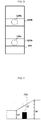
- FIG. 2 is a cross-sectional view illustrating a waveguide system according to an exemplary embodiment.
- FIG. 3 is a cutaway plane view illustrating the waveguide according to an exemplary embodiment.
- the waveguide includes the at least two step parts 120a and 120b at one side of the waveguide, and at the other side of the waveguide opposite to the step parts 120a and 120b, the block parts 130a and 130b protruding to the predetermined height from the other side.
- a block part 210 is configured to sit opposite to a step part 220 of a waveguide in which a height difference occurs.
- the step part 220 has at least two heights; one is a high height h1 and the other is a low height h2.
- a height of the block part 210 is, based on the low height h2, preferably from 30% to 70% of the low height of the waveguide. If the height of the block part 210 is less than the numerical range, an effect of microwave matching by the block part 210 reduces, and as microwaves of various wavelengths propagate simultaneously to the low height part of the step part, an effect of microwave concentration also reduces. In contrast, if the height of the block part 210 exceeds the numerical range, microwaves reflect by the block part 210 and the reflected microwaves interfere with incoming microwaves.
- the present disclosure provides a waveguide system using a cascade-shaped step part having a vertically decreasing height, rather than a step part of a tapering shape with a height decreasing at a predetermined angle, and simultaneously with a corresponding block part.
- the waveguide 300 has a plurality of step parts, and a block part of a predetermined height at an inner side surface of the waveguide opposite to a height boundary surface of the step parts.
- the block part is a separate member from the waveguide, and is disposed at the inner side surface of the waveguide as it is. Accordingly, a location of the block part is adjustable by a user in a simple manner based on a matching condition as shown in FIG. 6 , and further, because the block part does not penetrate into a wall of the waveguide, a problem of microwaves leaking out through the waveguide is prevented.
- the present disclosure may greatly increase a microwave density within the step part by matching microwaves of various frequencies generated and propagated from the waveguide. That is, the block part according to the present disclosure is not physically fixed at and coupled to the inner side surface of the waveguide, and is a separate member that may be disposed on the inner side surface.
- the separate member may be made from the same material as the waveguide or a different material from the waveguide, and according to necessity, any design change may be made based on a purpose of use of a plasma by changing its shape freely.
Landscapes
- Physics & Mathematics (AREA)
- Engineering & Computer Science (AREA)
- Plasma & Fusion (AREA)
- Electromagnetism (AREA)
- Spectroscopy & Molecular Physics (AREA)
- Chemical & Material Sciences (AREA)
- Analytical Chemistry (AREA)
- Plasma Technology (AREA)
- Waveguide Connection Structure (AREA)
- Drying Of Semiconductors (AREA)
Description
- The present disclosure relates to a plasma waveguide using a step part and a block part, and more particularly, to a plasma waveguide using a step part and a block part that may produce an effect of microwave matching while maximizing an effect of microwave concentration within the waveguide having a gradual reduction in height in a microwave propagation direction by using the step part simultaneously with the block part of a predetermined height provided at an inner side surface of the waveguide.
- A conventional plasma generator includes a waveguide to transmit electromagnetic waves, a 3-stub to tune a plasma impedance, and a plasma generation unit to generate a plasma, and the plasma generation unit is equipped with a discharge tube. When electromagnetic waves are transmitted to the waveguide, an electric field concentrates on the plasma generation unit of the waveguide where a plasma is generated.
- Accordingly, how to concentrate an electric field effectively is an important design factor of a waveguide.
- A waveguide has been developed on a trend toward gradual decrease in height from a traditional rectangular flat structure.
-
FIG. 1 is a full diagram illustrating a plasma reactor disclosed in Korean Patent Publication No.10-2008-0033408 - Referring to
FIG. 1 , a plasma reactor according to the related art 1 has a tapering shape with a height decreasing at a predetermined angle to concentrate an electric field (electromagnetic waves) being applied within a waveguide, and includes a reactor chamber at a rear end of the waveguide, in which a plasma is generated by application of the electric field. However, the related art 1 discloses the tapered waveguide designed to minimize reflection of electromagnetic waves, but in practice, an effect of electric field concentration in the chamber where the plasma is generated, is lower than that of the rear end of the waveguide. - To solve this problem, Korean Patent No.
10-1196966 - For fine tuning of microwaves, a 3-
stub matching system 20 is used as shown inFIG. 1 . - The 3-stub matching system has triple stubs installed at a stub interval of λg/4 when λg is a wavelength in a
waveguide 18, and serves to match a characteristic impedance of thewaveguide 18 with a load impedance of a low height part of thewaveguide 18 to transmit maximum power to a load. - However, such a 3-stub matching system is designed for maximum power transfer to a load in applications of a waveguide of a flat structure. Also, by a structure of the 3-stub matching system penetrating through the waveguide, leaks of a weak electromagnetic field out of the waveguide and its resultant arcing occur. To solve this problem, a high-cost sealing apparatus is separately required to prevent an electromagnetic field from leaking out of the waveguide.
-
US 2 432 094 A discloses an impedance transformer for waveguides wherein a rectangular section of a waveguide is interposed between two rectangular waveguides that differ in characteristic impedance. Hence, step parts are formed on two opposite sides of an inner side surface of the combined waveguide. In order to neutralize a capacitive effect of the stepped junction points, flaps are arranged at the junction points to introduce a shunt inductive reactance, hence, the height of these flaps correspond to the lowest heights of the corresponding step part formed by the junctions. -
US 4 891 614 discloses a waveguide with inductive and capacitive matching elements. The waveguide has a plurality of step parts formed at one first side of an inner side surface of the waveguide and a plurality of block parts forming capacitive elements that are arranged in predetermined distance from the step parts. -
US 2003/0020939 A1 shows a waveguide having a plurality of step parts which are taper parts with a height decreasing at a predetermined angle. This document forms the preamble of claim 1. -
WO 2012/121132 A1 discloses a plasma generating apparatus comprising a microwave generating apparatus, generating microwaves, and a rectangular waveguide which is connected to the microwave generating apparatus. Further, a phase shift apparatus is provided having a block part that can be introduced into the rectangular waveguide and retracted from the rectangular waveguide. - It is thus an object of the present disclosure to provide a novel plasma waveguide system with improved economic and technical efficiency.
- For solving this object, the invention proposes a magnetron and a plasma waveguide in accordance with claim 1.
- Advantageous embodiments are given in the dependent claims.
- In one embodiment, the step parts are a taper part with a height decreasing at a predetermined angle.
- In one embodiment, the block part is included within an area opposite to the taper part.
- In one embodiment, the block part is coupled with the inner side surface of the waveguide, and a location of the block part is adjustable.
- The present disclosure forms a step part having a height decreasing to a predetermined level within a waveguide, and provides a block part of a predetermined height at an inner side surface of the waveguide opposite to the step part of the waveguide. Thereby, a problem with microwave leaks involved in a 3-stub system penetrating through an overall waveguide and a problem with damage to an external system due to microwaves traveling outward may be effectively solved. Further, because the block part of the predetermined height provided at the inner side surface of the waveguide is located at an opposite surface to the step part, an effect of microwave concentration within the waveguide having a gradual reduction in height in a microwave propagation direction may be maximized.
-
-
FIG. 1 is a full diagram illustrating a plasma reactor disclosed in Korean Patent Publication No.10-2008-0033408 -
FIG. 2 is a cross-sectional view illustrating a waveguide system according to an exemplary embodiment. -
FIG. 3 is a cutaway plane view illustrating a waveguide according to an exemplary embodiment. -
FIG. 4 is a diagram illustrating a height ratio of a block part according to an exemplary embodiment. -
FIG. 5 is a diagram illustrating a waveguide system according to an exemplary embodiment. -
FIG. 6 is a cross-sectional view illustrating a waveguide including a block part according to an exemplary embodiment. - To solve the above problem, the present disclosure forms a step part having a height decreasing to a predetermined level within a waveguide, and provides a block part of a predetermined height at an inner side surface of the waveguide opposite to the step part of the waveguide. Thereby, a problem with microwave leaks involved in a 3-stub system penetrating through an overall waveguide and a problem with damage to an external system due to microwaves traveling outward may be effectively solved. Further, because the block part of the predetermined height provided at the inner side surface of the waveguide is located at an opposite surface to the step part, an effect of microwave concentration within the waveguide having a gradual reduction in height in a microwave propagation direction is maximized.
- Hereinafter, a waveguide system according to the present disclosure is described in detail using the drawings.
-
FIG. 2 is a cross-sectional view illustrating a waveguide system according to an exemplary embodiment. - Referring to
FIG. 2 , the waveguide system according to an exemplary embodiment includes amagnetron 110 from which microwaves are generated. The microwaves generated from themagnetron 110 propagate in one direction inside awaveguide 100, and in this instance, the waveguide system has at least onestep part FIG. 2 . - Particularly, the Inventor discovered that, in the case of a conventional waveguide of a double taper structure which has been published and registered, a substantial effect of microwave concentration was not high, and further, microwaves concentrated on only a reduced height part (that is, a rear end of a taper) of a waveguide, which in turn, an increase in microwave density was not achieved throughout the overall waveguide. Further, in case a 3-stub matching system penetrating through a waveguide from an outside is used in a waveguide of a double taper structure, the Inventor found out a problem with microwave leaks at stub penetration regions by reflection of unconcentrated microwaves or the like, causing damage to an external equipment.
- To solve the problem, the plasma waveguide system according to an exemplary embodiment has
block parts step parts - In an exemplary embodiment, a number of the
block parts FIG. 2 , the waveguide has the twotapered step parts block parts -
FIG. 3 is a cutaway plane view illustrating the waveguide according to an exemplary embodiment. - Referring to
FIG. 3 , the waveguide according to an exemplary embodiment includes the at least twostep parts step parts block parts - In an exemplary embodiment, locations of the
block parts tapered step parts - In the present disclosure, the height of the block parts is very important in an effect of microwave concentration and matching at the step part, and its description is provided below.
-
FIG. 4 is a diagram illustrating a height ratio of the block part according to an exemplary embodiment. - Referring to
FIG. 4 , ablock part 210 according to an exemplary embodiment is configured to sit opposite to astep part 220 of a waveguide in which a height difference occurs. - The
step part 220 has at least two heights; one is a high height h1 and the other is a low height h2. In this instance, a height of theblock part 210 is, based on the low height h2, preferably from 30% to 70% of the low height of the waveguide. If the height of theblock part 210 is less than the numerical range, an effect of microwave matching by theblock part 210 reduces, and as microwaves of various wavelengths propagate simultaneously to the low height part of the step part, an effect of microwave concentration also reduces. In contrast, if the height of theblock part 210 exceeds the numerical range, microwaves reflect by theblock part 210 and the reflected microwaves interfere with incoming microwaves. - Accordingly, preferably, the block part used at a location opposite to the step part is so high as to limit the lowest height part of the step part to a predetermined level, and an effect of microwave matching/concentration by the simultaneous use of the step part and the block part is maximized.
- Further, the present disclosure provides a waveguide system using a cascade-shaped step part having a vertically decreasing height, rather than a step part of a tapering shape with a height decreasing at a predetermined angle, and simultaneously with a corresponding block part.
-
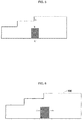
FIG. 5 is a diagram illustrating a waveguide system according to an exemplary embodiment. - Referring to
FIG. 5 , a waveguide includes a plurality of step parts having a vertically decreasing height, and a block part of a predetermined height at an inner side surface of the waveguide opposite to the step parts. - In such construction, an area (a) having the block part is configured to include a surface (b') opposite to a boundary surface of the step parts (that is, a waveguide location (b) at which a height reduction occurs). Thereby, similar to a block part included within a taper area, an effect of microwave concentration and matching may be maximized within the waveguide area in which the taper and the block part are provided simultaneously.
- In another exemplary embodiment, the block part is a separate member that is not physically coupled to the waveguide, and its location is adjustable.
-
FIG. 6 is a cross-sectional view illustrating a waveguide including a block part according to an exemplary embodiment. - Referring to
FIG. 6 , thewaveguide 300 has a plurality of step parts, and a block part of a predetermined height at an inner side surface of the waveguide opposite to a height boundary surface of the step parts. In this instance, the block part is a separate member from the waveguide, and is disposed at the inner side surface of the waveguide as it is. Accordingly, a location of the block part is adjustable by a user in a simple manner based on a matching condition as shown inFIG. 6 , and further, because the block part does not penetrate into a wall of the waveguide, a problem of microwaves leaking out through the waveguide is prevented. - As described hereinabove, through a step part and a block part of a predetermined height as a separate member provided at one side of the waveguide opposite to the step part, the present disclosure may greatly increase a microwave density within the step part by matching microwaves of various frequencies generated and propagated from the waveguide. That is, the block part according to the present disclosure is not physically fixed at and coupled to the inner side surface of the waveguide, and is a separate member that may be disposed on the inner side surface. Thus, the separate member may be made from the same material as the waveguide or a different material from the waveguide, and according to necessity, any design change may be made based on a purpose of use of a plasma by changing its shape freely.
- It should be understood that unless specially stated to the contrary, the terms "including", "comprising", or "having" used herein specify the presence of stated components, but do not preclude the presence or addition of one or more other components. Unless otherwise defined, all terms including technical and scientific terms used herein have the same meaning as commonly understood by one of ordinary skill in the art to which this invention belongs. It will be further understood that terms, such as those defined in commonly used dictionaries, should be interpreted as having a meaning that is consistent with their meaning in the context of the relevant art and will not be interpreted in an idealized or overly formal sense unless expressly so defined herein.
<Reference Sign List> 100: Waveguide 110: Magnetron 120a, 120b, 220: Step parts 130a, 130b, 210: Block parts 300: Waveguide
Claims (5)
- A magnetron (110) and a plasma waveguide (100, 300) for a plasma reactor wherein the magnetron is configured to generate a microwave arranged to move through the plasma waveguide (100, 300), the plasma waveguide (100, 300) comprising:a plurality of step parts (120a, 120b, 220) formed at a first side on an inner surface of the waveguide (100, 300) wherein the step parts (120a, 120b, 220) have at least a high height (h1) and a low height (h2) so that the step parts (120a, 120b, 220) represent structures in which an effective height within the waveguide reduces in a microwave propagation direction for effecting a microwave concentration;characterized in that a block part (130a, 130b, 210) is formed at a second side on the inner surface of the waveguide in a position opposite to each of the step parts (120a, 120b, 220), or in a position opposite to a boundary surface between two step parts and protruding to a predetermined height from the second side, andin that the height of the block part (130a, 130b, 210) occupies from 30% to 70% of the low height (h2) of the step parts (120a, 120b, 220).
- The magnetron (110) and plasma waveguide (100, 300) according to claim 1, wherein the step parts (120a, 120b, 220) are taper parts with a height decreasing at a predetermined angle.
- The magnetron (110) and plasma waveguide (100, 300) according to claim 2, wherein the block part (130a, 130b, 210) is included within an area opposite to the taper part.
- The magnetron (110) and plasma waveguide (100, 300) according to any of the claims 1 to 3, wherein the block part (130a, 130b, 210) is coupled with the inner surface of the waveguide (100, 300).
- The magnetron and plasma waveguide according to any of the claims 1 to 4, wherein the block part (130a, 130b, 210) is a separate member that is not physically coupled with the inner surface of the waveguide (100, 300), and a location of the block part (130a, 130b, 210) is adjustable in the microwave propagation direction.
Applications Claiming Priority (1)
| Application Number | Priority Date | Filing Date | Title |
|---|---|---|---|
| KR1020130032748A KR101427720B1 (en) | 2013-03-27 | 2013-03-27 | Plasma waveguide using step part and block part |
Publications (3)
| Publication Number | Publication Date |
|---|---|
| EP2785153A2 EP2785153A2 (en) | 2014-10-01 |
| EP2785153A3 EP2785153A3 (en) | 2014-11-05 |
| EP2785153B1 true EP2785153B1 (en) | 2019-05-01 |
Family
ID=50440471
Family Applications (1)
| Application Number | Title | Priority Date | Filing Date |
|---|---|---|---|
| EP14161587.2A Active EP2785153B1 (en) | 2013-03-27 | 2014-03-25 | Plasma waveguide using step part and block part |
Country Status (6)
| Country | Link |
|---|---|
| US (1) | US9576774B2 (en) |
| EP (1) | EP2785153B1 (en) |
| JP (1) | JP5767356B2 (en) |
| KR (1) | KR101427720B1 (en) |
| CN (1) | CN104078735B (en) |
| TW (1) | TWI563720B (en) |
Families Citing this family (3)
| Publication number | Priority date | Publication date | Assignee | Title |
|---|---|---|---|---|
| EP3571900B1 (en) | 2017-01-18 | 2024-11-13 | SHINE Technologies, LLC | Device comprising a waveguide with an inverted impedance matcher and system with the same |
| CN114050389B (en) * | 2021-12-01 | 2022-10-21 | 散裂中子源科学中心 | High-power ferrite load |
| CN119401969B (en) * | 2025-01-03 | 2025-04-29 | 成都沃特塞恩电子技术有限公司 | Automatic impedance matching method, device, system and microwave equipment |
Family Cites Families (31)
| Publication number | Priority date | Publication date | Assignee | Title |
|---|---|---|---|---|
| NL73887C (en) * | 1942-07-30 | |||
| GB2193044B (en) * | 1986-05-29 | 1990-09-19 | Nat Res Dev | Matching one or more asymmetrical discontinuities in transmission lines |
| US4866346A (en) * | 1987-06-22 | 1989-09-12 | Applied Science & Technology, Inc. | Microwave plasma generator |
| DE3803355A1 (en) * | 1988-02-05 | 1989-08-17 | Leybold Ag | PARTICLE SOURCE FOR A REACTIVE ION BEAM OR PLASMA POSITIONING PLANT |
| US4851630A (en) * | 1988-06-23 | 1989-07-25 | Applied Science & Technology, Inc. | Microwave reactive gas generator |
| JPH0495394A (en) * | 1990-06-28 | 1992-03-27 | Nippon Steel Corp | Method for forming electron cyclotron resonant plasma and processing apparatus for the same |
| US5804033A (en) * | 1990-09-26 | 1998-09-08 | Hitachi, Ltd. | Microwave plasma processing method and apparatus |
| EP0502269A1 (en) * | 1991-03-06 | 1992-09-09 | Hitachi, Ltd. | Method of and system for microwave plasma treatments |
| KR930020761A (en) * | 1992-03-06 | 1993-10-20 | 강진구 | Waveguide Structure of Microwave Heating Equipment |
| US5389153A (en) * | 1993-02-19 | 1995-02-14 | Texas Instruments Incorporated | Plasma processing system using surface wave plasma generating apparatus and method |
| TW264601B (en) * | 1993-09-17 | 1995-12-01 | Hitachi Seisakusyo Kk | |
| US6174424B1 (en) * | 1995-11-20 | 2001-01-16 | Cirrex Corp. | Couplers for optical fibers |
| US6031333A (en) * | 1996-04-22 | 2000-02-29 | Fusion Lighting, Inc. | Compact microwave lamp having a tuning block and a dielectric located in a lamp cavity |
| JPH1083896A (en) * | 1996-09-06 | 1998-03-31 | Hitachi Ltd | Plasma processing equipment |
| JP3878267B2 (en) * | 1996-12-27 | 2007-02-07 | 株式会社ダイヘン | Plasma processing equipment |
| US6706334B1 (en) * | 1997-06-04 | 2004-03-16 | Tokyo Electron Limited | Processing method and apparatus for removing oxide film |
| KR100375423B1 (en) * | 2000-09-27 | 2003-03-15 | 홍용철 | Plasma device for removing exhaust gas from diesel engine |
| WO2004033753A1 (en) * | 2002-10-09 | 2004-04-22 | Toyo Seikan Kaisha,Ltd. | Method of forming metal oxide film and microwave power source unit for use in the method |
| JP3996880B2 (en) * | 2003-07-29 | 2007-10-24 | 京セラ株式会社 | Waveguide branch structure |
| JP4390604B2 (en) * | 2004-03-19 | 2009-12-24 | 株式会社 液晶先端技術開発センター | Plasma processing equipment |
| GB0516695D0 (en) | 2005-08-15 | 2005-09-21 | Boc Group Plc | Microwave plasma reactor |
| JP4703371B2 (en) * | 2005-11-04 | 2011-06-15 | 国立大学法人東北大学 | Plasma processing equipment |
| GB0907947D0 (en) * | 2009-05-08 | 2009-06-24 | Ceravision Ltd | Light source |
| KR101065793B1 (en) * | 2009-07-10 | 2011-09-20 | 엘지전자 주식회사 | Electrodeless lighting equipment |
| KR101196966B1 (en) | 2010-01-28 | 2012-11-05 | (주)트리플코어스코리아 | Atmospheric plasma equipment and waveguide for the same |
| KR20110088658A (en) * | 2010-01-29 | 2011-08-04 | (주)에스피에스 | Plasma Generator Using Electromagnetic Wave and Waveguide for the Same |
| JP5921241B2 (en) * | 2011-03-10 | 2016-05-24 | 国立大学法人名古屋大学 | Plasma generating apparatus, plasma processing apparatus, and plasma processing method |
| US8653911B2 (en) * | 2011-07-22 | 2014-02-18 | Triple Cores Korea | Atmospheric plasma equipment and waveguide for the same |
| JP2013026118A (en) * | 2011-07-25 | 2013-02-04 | Triplecores Korea | Normal pressure plasma device and waveguide therefor |
| WO2013125260A1 (en) * | 2012-02-23 | 2013-08-29 | 東京エレクトロン株式会社 | Plasma processing device and high-frequency generator |
| US9273393B2 (en) * | 2014-01-25 | 2016-03-01 | Yuri Glukhoy | Torch system for depositing protective coatings on interior walls and recesses present on the flat surface of an object |
-
2013
- 2013-03-27 KR KR1020130032748A patent/KR101427720B1/en active Active
-
2014
- 2014-03-20 TW TW103110533A patent/TWI563720B/en active
- 2014-03-25 JP JP2014061315A patent/JP5767356B2/en active Active
- 2014-03-25 EP EP14161587.2A patent/EP2785153B1/en active Active
- 2014-03-26 US US14/225,693 patent/US9576774B2/en active Active
- 2014-03-26 CN CN201410116865.4A patent/CN104078735B/en active Active
Non-Patent Citations (1)
| Title |
|---|
| None * |
Also Published As
| Publication number | Publication date |
|---|---|
| EP2785153A3 (en) | 2014-11-05 |
| CN104078735A (en) | 2014-10-01 |
| TW201440310A (en) | 2014-10-16 |
| TWI563720B (en) | 2016-12-21 |
| JP5767356B2 (en) | 2015-08-19 |
| CN104078735B (en) | 2017-05-24 |
| US9576774B2 (en) | 2017-02-21 |
| US20140292195A1 (en) | 2014-10-02 |
| JP2014192158A (en) | 2014-10-06 |
| KR101427720B1 (en) | 2014-08-13 |
| EP2785153A2 (en) | 2014-10-01 |
Similar Documents
| Publication | Publication Date | Title |
|---|---|---|
| US10916849B2 (en) | Dual-band antenna | |
| EP2351151B1 (en) | Horn antenna, waveguide or apparatus including low index dielectric material | |
| CN101694903B (en) | Dual-arm coupling quadrature mode coupler with high cross polarization discrimination | |
| CN104716407B (en) | Microwave mode converter | |
| CN104979638A (en) | Dual-band and dual-polarization millimeter wave feed source | |
| US11881622B2 (en) | Antenna element with filtering function, filtering radiation unit, and antenna | |
| CA2869200A1 (en) | Waveguide circulator having stepped floor/ceiling and quarter-wave dielectric transformer | |
| US9576774B2 (en) | Plasma wavguide using step part and block part | |
| CN117153647A (en) | H-face ultra-compact strip-shaped traveling wave tube coupler with arc resonator | |
| CN205029021U (en) | Open ended waveguide antenna array unit and system with calibrate function | |
| CN104051205A (en) | Novel gyro traveling-wave tube coupling input structure | |
| CN205029020U (en) | Dual -frenquency double polarization millimeter wave feed | |
| CN109786970B (en) | A kind of X/Ka multi-frequency broadband multi-mode feed | |
| Hijazi et al. | 3D-Printed Ultra-Wideband In-Band Full-Duplex Antenna System with Grating Lobes Reduction | |
| JP6391415B2 (en) | Waveguide bandstop filter | |
| CN110190380A (en) | A kind of radio frequency snail orbital angular momentum antenna based on annular pin array | |
| EP3091611B1 (en) | Antenna and wireless device | |
| KR101724215B1 (en) | Traveling wave antenna with rectangular waveguide feeding structure | |
| CN113365380A (en) | Structural member for radiation heating, assembly and heating equipment | |
| CN105322260A (en) | Electromagnetic Mode Converter | |
| Letizia et al. | Photonic bandgap coupler for 346 GHz sheet-beam BWO | |
| CN105609934A (en) | Terahertz circularly polarized antenna | |
| CN118249093A (en) | Broadband pattern diversity antenna and communication system based on rectangular micro-coaxial technology | |
| CN121584255A (en) | Leakage cable based on symmetrical slots to suppress higher-order modes | |
| Li et al. | Improvement of the radiation and impedance performance for the dielectric rod antenna |
Legal Events
| Date | Code | Title | Description |
|---|---|---|---|
| 17P | Request for examination filed |
Effective date: 20140325 |
|
| AK | Designated contracting states |
Kind code of ref document: A2 Designated state(s): AL AT BE BG CH CY CZ DE DK EE ES FI FR GB GR HR HU IE IS IT LI LT LU LV MC MK MT NL NO PL PT RO RS SE SI SK SM TR |
|
| AX | Request for extension of the european patent |
Extension state: BA ME |
|
| PUAI | Public reference made under article 153(3) epc to a published international application that has entered the european phase |
Free format text: ORIGINAL CODE: 0009012 |
|
| PUAL | Search report despatched |
Free format text: ORIGINAL CODE: 0009013 |
|
| AK | Designated contracting states |
Kind code of ref document: A3 Designated state(s): AL AT BE BG CH CY CZ DE DK EE ES FI FR GB GR HR HU IE IS IT LI LT LU LV MC MK MT NL NO PL PT RO RS SE SI SK SM TR |
|
| AX | Request for extension of the european patent |
Extension state: BA ME |
|
| RIC1 | Information provided on ipc code assigned before grant |
Ipc: H01P 5/02 20060101ALI20141001BHEP Ipc: H05H 1/46 20060101AFI20141001BHEP Ipc: H01J 37/32 20060101ALI20141001BHEP Ipc: H03C 7/02 20060101ALI20141001BHEP |
|
| R17P | Request for examination filed (corrected) |
Effective date: 20150504 |
|
| RBV | Designated contracting states (corrected) |
Designated state(s): AL AT BE BG CH CY CZ DE DK EE ES FI FR GB GR HR HU IE IS IT LI LT LU LV MC MK MT NL NO PL PT RO RS SE SI SK SM TR |
|
| GRAP | Despatch of communication of intention to grant a patent |
Free format text: ORIGINAL CODE: EPIDOSNIGR1 |
|
| STAA | Information on the status of an ep patent application or granted ep patent |
Free format text: STATUS: GRANT OF PATENT IS INTENDED |
|
| INTG | Intention to grant announced |
Effective date: 20181105 |
|
| GRAS | Grant fee paid |
Free format text: ORIGINAL CODE: EPIDOSNIGR3 |
|
| GRAA | (expected) grant |
Free format text: ORIGINAL CODE: 0009210 |
|
| STAA | Information on the status of an ep patent application or granted ep patent |
Free format text: STATUS: THE PATENT HAS BEEN GRANTED |
|
| AK | Designated contracting states |
Kind code of ref document: B1 Designated state(s): AL AT BE BG CH CY CZ DE DK EE ES FI FR GB GR HR HU IE IS IT LI LT LU LV MC MK MT NL NO PL PT RO RS SE SI SK SM TR |
|
| REG | Reference to a national code |
Ref country code: GB Ref legal event code: FG4D |
|
| REG | Reference to a national code |
Ref country code: CH Ref legal event code: EP Ref country code: AT Ref legal event code: REF Ref document number: 1128676 Country of ref document: AT Kind code of ref document: T Effective date: 20190515 |
|
| REG | Reference to a national code |
Ref country code: DE Ref legal event code: R096 Ref document number: 602014045619 Country of ref document: DE |
|
| REG | Reference to a national code |
Ref country code: IE Ref legal event code: FG4D |
|
| REG | Reference to a national code |
Ref country code: NL Ref legal event code: MP Effective date: 20190501 |
|
| REG | Reference to a national code |
Ref country code: LT Ref legal event code: MG4D |
|
| PG25 | Lapsed in a contracting state [announced via postgrant information from national office to epo] |
Ref country code: AL Free format text: LAPSE BECAUSE OF FAILURE TO SUBMIT A TRANSLATION OF THE DESCRIPTION OR TO PAY THE FEE WITHIN THE PRESCRIBED TIME-LIMIT Effective date: 20190501 Ref country code: PT Free format text: LAPSE BECAUSE OF FAILURE TO SUBMIT A TRANSLATION OF THE DESCRIPTION OR TO PAY THE FEE WITHIN THE PRESCRIBED TIME-LIMIT Effective date: 20190901 Ref country code: FI Free format text: LAPSE BECAUSE OF FAILURE TO SUBMIT A TRANSLATION OF THE DESCRIPTION OR TO PAY THE FEE WITHIN THE PRESCRIBED TIME-LIMIT Effective date: 20190501 Ref country code: LT Free format text: LAPSE BECAUSE OF FAILURE TO SUBMIT A TRANSLATION OF THE DESCRIPTION OR TO PAY THE FEE WITHIN THE PRESCRIBED TIME-LIMIT Effective date: 20190501 Ref country code: HR Free format text: LAPSE BECAUSE OF FAILURE TO SUBMIT A TRANSLATION OF THE DESCRIPTION OR TO PAY THE FEE WITHIN THE PRESCRIBED TIME-LIMIT Effective date: 20190501 Ref country code: NL Free format text: LAPSE BECAUSE OF FAILURE TO SUBMIT A TRANSLATION OF THE DESCRIPTION OR TO PAY THE FEE WITHIN THE PRESCRIBED TIME-LIMIT Effective date: 20190501 Ref country code: SE Free format text: LAPSE BECAUSE OF FAILURE TO SUBMIT A TRANSLATION OF THE DESCRIPTION OR TO PAY THE FEE WITHIN THE PRESCRIBED TIME-LIMIT Effective date: 20190501 Ref country code: NO Free format text: LAPSE BECAUSE OF FAILURE TO SUBMIT A TRANSLATION OF THE DESCRIPTION OR TO PAY THE FEE WITHIN THE PRESCRIBED TIME-LIMIT Effective date: 20190801 Ref country code: ES Free format text: LAPSE BECAUSE OF FAILURE TO SUBMIT A TRANSLATION OF THE DESCRIPTION OR TO PAY THE FEE WITHIN THE PRESCRIBED TIME-LIMIT Effective date: 20190501 |
|
| PG25 | Lapsed in a contracting state [announced via postgrant information from national office to epo] |
Ref country code: RS Free format text: LAPSE BECAUSE OF FAILURE TO SUBMIT A TRANSLATION OF THE DESCRIPTION OR TO PAY THE FEE WITHIN THE PRESCRIBED TIME-LIMIT Effective date: 20190501 Ref country code: BG Free format text: LAPSE BECAUSE OF FAILURE TO SUBMIT A TRANSLATION OF THE DESCRIPTION OR TO PAY THE FEE WITHIN THE PRESCRIBED TIME-LIMIT Effective date: 20190801 Ref country code: GR Free format text: LAPSE BECAUSE OF FAILURE TO SUBMIT A TRANSLATION OF THE DESCRIPTION OR TO PAY THE FEE WITHIN THE PRESCRIBED TIME-LIMIT Effective date: 20190802 Ref country code: LV Free format text: LAPSE BECAUSE OF FAILURE TO SUBMIT A TRANSLATION OF THE DESCRIPTION OR TO PAY THE FEE WITHIN THE PRESCRIBED TIME-LIMIT Effective date: 20190501 |
|
| REG | Reference to a national code |
Ref country code: AT Ref legal event code: MK05 Ref document number: 1128676 Country of ref document: AT Kind code of ref document: T Effective date: 20190501 |
|
| PG25 | Lapsed in a contracting state [announced via postgrant information from national office to epo] |
Ref country code: IS Free format text: LAPSE BECAUSE OF FAILURE TO SUBMIT A TRANSLATION OF THE DESCRIPTION OR TO PAY THE FEE WITHIN THE PRESCRIBED TIME-LIMIT Effective date: 20190901 |
|
| PG25 | Lapsed in a contracting state [announced via postgrant information from national office to epo] |
Ref country code: CZ Free format text: LAPSE BECAUSE OF FAILURE TO SUBMIT A TRANSLATION OF THE DESCRIPTION OR TO PAY THE FEE WITHIN THE PRESCRIBED TIME-LIMIT Effective date: 20190501 Ref country code: RO Free format text: LAPSE BECAUSE OF FAILURE TO SUBMIT A TRANSLATION OF THE DESCRIPTION OR TO PAY THE FEE WITHIN THE PRESCRIBED TIME-LIMIT Effective date: 20190501 Ref country code: DK Free format text: LAPSE BECAUSE OF FAILURE TO SUBMIT A TRANSLATION OF THE DESCRIPTION OR TO PAY THE FEE WITHIN THE PRESCRIBED TIME-LIMIT Effective date: 20190501 Ref country code: AT Free format text: LAPSE BECAUSE OF FAILURE TO SUBMIT A TRANSLATION OF THE DESCRIPTION OR TO PAY THE FEE WITHIN THE PRESCRIBED TIME-LIMIT Effective date: 20190501 Ref country code: EE Free format text: LAPSE BECAUSE OF FAILURE TO SUBMIT A TRANSLATION OF THE DESCRIPTION OR TO PAY THE FEE WITHIN THE PRESCRIBED TIME-LIMIT Effective date: 20190501 Ref country code: SK Free format text: LAPSE BECAUSE OF FAILURE TO SUBMIT A TRANSLATION OF THE DESCRIPTION OR TO PAY THE FEE WITHIN THE PRESCRIBED TIME-LIMIT Effective date: 20190501 |
|
| REG | Reference to a national code |
Ref country code: DE Ref legal event code: R097 Ref document number: 602014045619 Country of ref document: DE |
|
| PG25 | Lapsed in a contracting state [announced via postgrant information from national office to epo] |
Ref country code: IT Free format text: LAPSE BECAUSE OF FAILURE TO SUBMIT A TRANSLATION OF THE DESCRIPTION OR TO PAY THE FEE WITHIN THE PRESCRIBED TIME-LIMIT Effective date: 20190501 Ref country code: SM Free format text: LAPSE BECAUSE OF FAILURE TO SUBMIT A TRANSLATION OF THE DESCRIPTION OR TO PAY THE FEE WITHIN THE PRESCRIBED TIME-LIMIT Effective date: 20190501 |
|
| PLBE | No opposition filed within time limit |
Free format text: ORIGINAL CODE: 0009261 |
|
| STAA | Information on the status of an ep patent application or granted ep patent |
Free format text: STATUS: NO OPPOSITION FILED WITHIN TIME LIMIT |
|
| PG25 | Lapsed in a contracting state [announced via postgrant information from national office to epo] |
Ref country code: TR Free format text: LAPSE BECAUSE OF FAILURE TO SUBMIT A TRANSLATION OF THE DESCRIPTION OR TO PAY THE FEE WITHIN THE PRESCRIBED TIME-LIMIT Effective date: 20190501 |
|
| 26N | No opposition filed |
Effective date: 20200204 |
|
| PG25 | Lapsed in a contracting state [announced via postgrant information from national office to epo] |
Ref country code: PL Free format text: LAPSE BECAUSE OF FAILURE TO SUBMIT A TRANSLATION OF THE DESCRIPTION OR TO PAY THE FEE WITHIN THE PRESCRIBED TIME-LIMIT Effective date: 20190501 |
|
| PG25 | Lapsed in a contracting state [announced via postgrant information from national office to epo] |
Ref country code: SI Free format text: LAPSE BECAUSE OF FAILURE TO SUBMIT A TRANSLATION OF THE DESCRIPTION OR TO PAY THE FEE WITHIN THE PRESCRIBED TIME-LIMIT Effective date: 20190501 |
|
| PG25 | Lapsed in a contracting state [announced via postgrant information from national office to epo] |
Ref country code: MC Free format text: LAPSE BECAUSE OF FAILURE TO SUBMIT A TRANSLATION OF THE DESCRIPTION OR TO PAY THE FEE WITHIN THE PRESCRIBED TIME-LIMIT Effective date: 20190501 |
|
| REG | Reference to a national code |
Ref country code: CH Ref legal event code: PL |
|
| REG | Reference to a national code |
Ref country code: BE Ref legal event code: MM Effective date: 20200331 |
|
| PG25 | Lapsed in a contracting state [announced via postgrant information from national office to epo] |
Ref country code: LU Free format text: LAPSE BECAUSE OF NON-PAYMENT OF DUE FEES Effective date: 20200325 |
|
| PG25 | Lapsed in a contracting state [announced via postgrant information from national office to epo] |
Ref country code: LI Free format text: LAPSE BECAUSE OF NON-PAYMENT OF DUE FEES Effective date: 20200331 Ref country code: IE Free format text: LAPSE BECAUSE OF NON-PAYMENT OF DUE FEES Effective date: 20200325 Ref country code: CH Free format text: LAPSE BECAUSE OF NON-PAYMENT OF DUE FEES Effective date: 20200331 Ref country code: FR Free format text: LAPSE BECAUSE OF NON-PAYMENT OF DUE FEES Effective date: 20200331 |
|
| PG25 | Lapsed in a contracting state [announced via postgrant information from national office to epo] |
Ref country code: BE Free format text: LAPSE BECAUSE OF NON-PAYMENT OF DUE FEES Effective date: 20200331 |
|
| GBPC | Gb: european patent ceased through non-payment of renewal fee |
Effective date: 20200325 |
|
| PG25 | Lapsed in a contracting state [announced via postgrant information from national office to epo] |
Ref country code: GB Free format text: LAPSE BECAUSE OF NON-PAYMENT OF DUE FEES Effective date: 20200325 |
|
| PG25 | Lapsed in a contracting state [announced via postgrant information from national office to epo] |
Ref country code: MT Free format text: LAPSE BECAUSE OF FAILURE TO SUBMIT A TRANSLATION OF THE DESCRIPTION OR TO PAY THE FEE WITHIN THE PRESCRIBED TIME-LIMIT Effective date: 20190501 Ref country code: CY Free format text: LAPSE BECAUSE OF FAILURE TO SUBMIT A TRANSLATION OF THE DESCRIPTION OR TO PAY THE FEE WITHIN THE PRESCRIBED TIME-LIMIT Effective date: 20190501 |
|
| PG25 | Lapsed in a contracting state [announced via postgrant information from national office to epo] |
Ref country code: MK Free format text: LAPSE BECAUSE OF FAILURE TO SUBMIT A TRANSLATION OF THE DESCRIPTION OR TO PAY THE FEE WITHIN THE PRESCRIBED TIME-LIMIT Effective date: 20190501 |
|
| REG | Reference to a national code |
Ref country code: DE Ref legal event code: R081 Ref document number: 602014045619 Country of ref document: DE Owner name: TRIPLE CORES TECHNOLOGY CO., LTD., YONGIN-SI, KR Free format text: FORMER OWNER: TRIPLE CORES KOREA CO., LTD., YONGIN-SI, GYEONGGI-DO, KR |
|
| PGFP | Annual fee paid to national office [announced via postgrant information from national office to epo] |
Ref country code: DE Payment date: 20250417 Year of fee payment: 12 |