EP2784815A1 - Semiconductor device - Google Patents
Semiconductor device Download PDFInfo
- Publication number
- EP2784815A1 EP2784815A1 EP14153568.2A EP14153568A EP2784815A1 EP 2784815 A1 EP2784815 A1 EP 2784815A1 EP 14153568 A EP14153568 A EP 14153568A EP 2784815 A1 EP2784815 A1 EP 2784815A1
- Authority
- EP
- European Patent Office
- Prior art keywords
- semiconductor device
- electrode
- signal
- substrate
- slit
- Prior art date
- Legal status (The legal status is an assumption and is not a legal conclusion. Google has not performed a legal analysis and makes no representation as to the accuracy of the status listed.)
- Granted
Links
Images




Classifications
-
- H—ELECTRICITY
- H10—SEMICONDUCTOR DEVICES; ELECTRIC SOLID-STATE DEVICES NOT OTHERWISE PROVIDED FOR
- H10W—GENERIC PACKAGES, INTERCONNECTIONS, CONNECTORS OR OTHER CONSTRUCTIONAL DETAILS OF DEVICES COVERED BY CLASS H10
- H10W20/00—Interconnections in chips, wafers or substrates
- H10W20/20—Interconnections within wafers or substrates, e.g. through-silicon vias [TSV]
-
- H—ELECTRICITY
- H10—SEMICONDUCTOR DEVICES; ELECTRIC SOLID-STATE DEVICES NOT OTHERWISE PROVIDED FOR
- H10W—GENERIC PACKAGES, INTERCONNECTIONS, CONNECTORS OR OTHER CONSTRUCTIONAL DETAILS OF DEVICES COVERED BY CLASS H10
- H10W20/00—Interconnections in chips, wafers or substrates
- H10W20/40—Interconnections external to wafers or substrates, e.g. back-end-of-line [BEOL] metallisations or vias connecting to gate electrodes
- H10W20/41—Interconnections external to wafers or substrates, e.g. back-end-of-line [BEOL] metallisations or vias connecting to gate electrodes characterised by their conductive parts
- H10W20/423—Shielding layers
-
- H—ELECTRICITY
- H10—SEMICONDUCTOR DEVICES; ELECTRIC SOLID-STATE DEVICES NOT OTHERWISE PROVIDED FOR
- H10W—GENERIC PACKAGES, INTERCONNECTIONS, CONNECTORS OR OTHER CONSTRUCTIONAL DETAILS OF DEVICES COVERED BY CLASS H10
- H10W20/00—Interconnections in chips, wafers or substrates
- H10W20/40—Interconnections external to wafers or substrates, e.g. back-end-of-line [BEOL] metallisations or vias connecting to gate electrodes
- H10W20/495—Capacitive arrangements or effects of, or between wiring layers
- H10W20/496—Capacitor integral with wiring layers
-
- H—ELECTRICITY
- H10—SEMICONDUCTOR DEVICES; ELECTRIC SOLID-STATE DEVICES NOT OTHERWISE PROVIDED FOR
- H10W—GENERIC PACKAGES, INTERCONNECTIONS, CONNECTORS OR OTHER CONSTRUCTIONAL DETAILS OF DEVICES COVERED BY CLASS H10
- H10W44/00—Electrical arrangements for controlling or matching impedance
- H10W44/20—Electrical arrangements for controlling or matching impedance at high-frequency [HF] or radio frequency [RF]
-
- H—ELECTRICITY
- H10—SEMICONDUCTOR DEVICES; ELECTRIC SOLID-STATE DEVICES NOT OTHERWISE PROVIDED FOR
- H10W—GENERIC PACKAGES, INTERCONNECTIONS, CONNECTORS OR OTHER CONSTRUCTIONAL DETAILS OF DEVICES COVERED BY CLASS H10
- H10W44/00—Electrical arrangements for controlling or matching impedance
- H10W44/20—Electrical arrangements for controlling or matching impedance at high-frequency [HF] or radio frequency [RF]
- H10W44/203—Electrical connections
-
- H—ELECTRICITY
- H10—SEMICONDUCTOR DEVICES; ELECTRIC SOLID-STATE DEVICES NOT OTHERWISE PROVIDED FOR
- H10W—GENERIC PACKAGES, INTERCONNECTIONS, CONNECTORS OR OTHER CONSTRUCTIONAL DETAILS OF DEVICES COVERED BY CLASS H10
- H10W44/00—Electrical arrangements for controlling or matching impedance
- H10W44/20—Electrical arrangements for controlling or matching impedance at high-frequency [HF] or radio frequency [RF]
- H10W44/241—Electrical arrangements for controlling or matching impedance at high-frequency [HF] or radio frequency [RF] for passive devices or passive elements
- H10W44/243—Electrical arrangements for controlling or matching impedance at high-frequency [HF] or radio frequency [RF] for passive devices or passive elements for decoupling, e.g. bypass capacitors
Definitions
- a semiconductor device that processes an ultra-high frequency signal of a millimeterwave and the like may been put in practical use.
- the wavelength of a signal (radio frequency (RF) signal) becomes short as the operating frequency of the signal becomes high.
- a resonant mode occurs between the rear face of the chip and the circuit pattern of a front face.
- the output signal is fed back to the input terminal due to the resonance, which causes the oscillation or the deterioration of the band characteristic or the like.
- a multilayer wiring structure in which a ground plane (GND shield) is arranged in a lower layer so that a substrate is shielded from a signal electrode (pad electrode) in order to establish a structure that prevents an RF signal from leaking to the substrate.
- GND shield ground plane
- pad electrode signal electrode
- the GND shield is arranged in the lower layer of the pad electrode, e.g., the deterioration of a high frequency characteristic will be caused by a capacitance between the pad electrode and the GND shield.
- Patent Document 1 Japanese Laid-open Patent Publication No. 2003-224189
- a semiconductor device includes a first electrode formed on a substrate, the first electrode being a first electrical potential; and a second electrode formed on the first electrode, the second electrode including a signal wiring that transmits a signal and a planar electrode part with a prescribed area.
- a shape of the first electrode corresponding to the planar electrode part is made into a slit shape such that a longitudinal direction of a slit is parallel to a direction in which the signal proceeds in the planar electrode part.
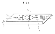
- FIG. 1 is a schematic diagram depicting an example of a semiconductor device.
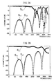
- FIGS. 2A and 2B depict examples of the dependence of S-parameter vs. frequency for different substrate thicknesses in the semiconductor device depicted in FIG. 1 .
- FIGS. 2A and 2B depict simulation results for the substrate thickness of 100 ⁇ m and of 50 ⁇ m, respectively.
- reference sign 1 denotes a substrate (semiconductor substrate)
- reference sign 2 denotes an amplifier
- reference sign D denotes a substrate thickness.
- S-parameters (Scattering parameters) S 11 , S 22 and S 21 are defined as follows.
- S 11 represents an S-parameter which is detected (reflected) from the input IN for an incidence to the input IN
- S 22 represents an S-parameter which is detected from the output OUT for an incidence to the output OUT
- S 21 represents an S-parameter which is detected from the output OUT for an incidence to the input IN.
- both of the S-parameter S 11 representing the reflection of the input and the S-parameter S 22 representing the reflection of the output increase abruptly, e.g., at around a frequency exceeding 200 GHz.
- the S-parameter S 21 representing the passage of a signal through the semiconductor device, in which the signal input into the input IN is amplified by the amplifier 2 and is output from the output OUT, begins to decrease, e.g., at around a frequency exceeding 200 GHz, and becomes smaller than the S-parameters S 11 and S 22 art around 220 GHz.
- the S-parameter S 21 temporarily becomes larger than the S-parameters S 11 and S 22 , e.g., at around 240 GHz, but may be a minimum value (-30dB) at around 300 GHz, indicating that the signal may hardly pass through the semiconductor device. Accordingly, when the thickness D of the substrate 1 is 100 ⁇ m, it is difficult to use the semiconductor device up to 300 GHz, and a use frequency will be almost restricted to 200 GHz or less.
- the S-parameters S 11 and S 22 increase, e.g., as the frequency becomes high, and become larger than the S-parameter S 21 at frequencies exceeding 300 GHz.
- the S-parameter S 21 varies so that it exhibits an opposite characteristic for a frequency change as compared to those of the S-parameters S 11 and S 22 , and becomes smaller than the S-parameters S 11 and S 22 at frequencies exceeding about 300 GHz, as mentioned above. Accordingly, the semiconductor device is usable up to about 300 GHz, but its characteristic deteriorates due to large reflection at frequencies exceeding 300 GHz.
- a microstripline structure is applied, e.g., in which shielding is performed by a ground wiring.
- FIGS. 3A and 3B are explanatory diagrams for a microstripline structure in a semiconductor device.
- FIG. 3A depicts a cross section of a microstripline structure
- FIG. 3B depicts an example of the dependence of each S-parameter vs. frequency in the microstripline structure depicted in FIG. 3A .
- reference sign 1 denotes a substrate
- reference sign 11 denotes a ground wiring (GND shield)
- reference sign 12 denotes an insulating layer
- reference sign 13 denotes a signal wiring.
- the ground wiring (GND shield) 11 on which a ground (GND) electrical potential is applied by a metal wiring layer, is formed on the substrate 1.
- the signal wiring 13 by a metal wiring layer is formed on the GND shield 11 via the insulating layer 12.
- a distance between the GND shield 11 and the signal wiring 13, i.e., the thickness d of the insulating layer 12, is about 1 ⁇ m, and the thickness D of the substrate 1 is about 100 ⁇ m.
- the S-parameter S 12 which represents the passage of a signal through the semiconductor device, hardly decreases and maintains 0 dB even when the frequency increases and, e.g., exceeds 300 GHz.
- the S-parameters S 11 and S 22 which represent the reflection of the input and the output respectively, vary, e.g., in a range between -20 dB and -30 dB with the period of about 100 GHz, the S-parameters do not increase drastically. In other words, it is understandable that the microstripline structure enables a good signal transmission even for a signal with a frequency exceeding 300 GHz.
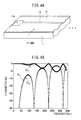
- FIGS. 4A and 4B are explanatory diagrams for a GND shield structure in a semiconductor device.
- FIG. 4A depicts a perspective view
- FIG. 4B depicts an example of the dependence of each S-parameter vs. frequency in the GND structure depicted in FIG. 4A .
- FIG. 4A depicts a part (end part) of the substrate 1.
- a GND shield 11 on which a GND electrical potential is applied by a metal wiring, is formed on a substrate 1, in a similar manner to that of the microstripline structure of FIG. 3A mentioned above.
- a signal wiring 13 by a metal wiring layer is formed on the GND shield 11 via an insulating layer 12.
- a distance between the GND shield 11 and the signal wiring 13, i.e. the thickness d of the insulating layer, is about 1 ⁇ m, and the thickness D of the substrate 1 is about 100 ⁇ m.
- a planar electrode part (pad electrode) 13a which may be an area of a certain size for an input/output pad and the like, is typically formed on the end part of the signal wiring 13. Since the pad electrode 13a like this faces the GND shield 11 via the insulating layer 12, a capacitance is to be formed.
- the S-parameter S 21 almost coincides with the S-parameters S 11 , S 22 at around 180 GHz, originating from the capacitance formed by the pad electrode 13a.
- the magnitude of attenuation of a signal passing through the semiconductor device becomes substantially equal to the magnitude of attenuation of a signal reflected at an input/output terminal.
- the S-parameters S 11 and S 22 become larger than the S-parameter S 21 , in other words, a signal passing through the semiconductor device becomes smaller than a signal reflected from the input/output terminal.
- arranging the GND shield 11 in the lower layer of the pad electrode 13a causes the deterioration of a high frequency characteristic by the capacitance, e.g., between the pad electrode 13a and the GND shield 11.
- FIGS. 5A and 5B are explanatory diagrams for the semiconductor device of a first embodiment.
- FIG. 5A depicts a perspective view
- FIG. 5B depicts an example of the dependence of each S-parameter vs. frequency in a GND shield structure depicted in FIG. 5A.
- FIG. 5A depicts a part (end part) of a semiconductor substrate (substrate) 1.
- a GND shield 11 on which a ground (GND) electrical potential by a metal wiring layer on the substrate 1 is applied, is formed in a slit shape (reed shape) in the periphery of the substrate 1 on which a pad electrode 13a is provided.
- the slit parts 11a of the GND shield 11 may not be formed, e.g., on all the periphery of the substrate 1 on which the input/output pad electrode is arranged, but may be formed on an area corresponding to the pad electrode 13a, and a solid shape one may be formed on other area.
- the GND shield 11 corresponding to the pad electrode 13a is made into the slit shape (the slit parts) 11a, such that a longitudinal direction of a slit is in parallel to a direction in which the signal proceeds in the pad electrode 13a.
- the longitudinal direction of the slit parts 11a of the GND shield 11 is in agreement with a direction in which a signal wiring 13, which connects to the pad electrode 13a, extends from the pad electrode 13a.
- an insulating layer 12 is provided, as depicted in FIG. 3A mentioned above.
- the thickness d of the insulating layer 12 is one-fourth of a signal wavelength or less.
- a pitch P between each of the slit parts 11a of the GND shield 11 is also one-fourth of the signal wavelength or less.
- the wavelength (length per one wave) of a signal corresponds to a value that is obtained, e.g., when a velocity at which the signal is propagated on the substrate 1 is divided by the frequency of the signal.
- the S-parameter S 21 is sufficiently larger than the S-parameters S 11 and S 22 .
- this is because an electric field is generated between the pad electrode 13a and the slit parts 11a of the GND shield 11 and the leakage of a signal (RF signal) to the substrate 1 may be reduced.
- the capacitance may be reduced by decreasing an area opposite to the pad electrode 13a, and the deterioration of a high frequency characteristic may be suppressed. Accordingly, it is understandable that the semiconductor device of the first embodiment is usable in all the bands, e.g., of the signal frequency of 0 to 350 GHz.
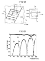
- FIGS. 6A and 6B depict a pad part and an example of the dependence of each S-parameter vs. frequency, respectively, in the semiconductor device depicted in FIGS. 5A and 5B .
- FIGS. 6A and 6B depict a case where the longitudinal direction of the slit parts 11a of the GND shield 11 is in agreement with a direction in which a signal proceeds in the pad electrode 13a, as is the case of FIGS. 5A and 5B mentioned above.
- FIG. 6A depicts the shape of the slit parts 11a
- FIG. 6B depicts an example of the dependence of each S-parameter vs. frequency in that case.
- FIGS. 7A and 7B depict a case where the longitudinal direction of the slit parts 11a of the GND shield 11 is perpendicular to a direction in which a signal proceeds in the pad electrode 13a.
- FIG. 7A depicts the shape of the slit parts 11a
- FIG. 7B depicts an example of the dependence of each S-parameter vs. frequency in that case. Note that in FIG. 7A , a plurality of slits 11c are connected with the GND shield 11, e.g., by a connecting wiring 11d, receiving a same electrical potential (GND-level electrical potential).
- Reference sign 10 denotes a signal supply pad in FIGS. 6B and 7B , and supplying a signal from the signal supply pad 10 causes the signal to flow (proceed) from the signal supply pad 10 toward the signal wiring 13 in the pad electrode 13a.
- a shielding effect may be confirmed when the direction of the slit parts 11a of the GND shield 11 is in agreement with the direction in which the signal proceeds in the pad electrode 13a, but the shielding effect may not be confirmed when the direction of the slit part 11a is perpendicular to the direction in which the signal proceeds.
- the slit parts 11a of the GND shield 11 and preferably formed so that that the direction thereof is in agreement with (in parallel with) the direction in which the signal proceeds in the pad electrode 13a.
- FIG. 8 is an explanatory diagram for the semiconductor device of a second embodiment, depicting an example in which a capacitance such as an MIM (Metal-Insulator-Metal) capacitor is formed on a substrate 1 by pad electrodes (planar electrode parts) 13b and 14b of two wirings 13 and 14 provided in parallel with each other.
- a capacitance such as an MIM (Metal-Insulator-Metal) capacitor is formed on a substrate 1 by pad electrodes (planar electrode parts) 13b and 14b of two wirings 13 and 14 provided in parallel with each other.
- MIM Metal-Insulator-Metal
- an insulating layer (dielectric layer) is provided between the pad electrode 13b and the pad electrode 14b, and a capacitance is formed by a structure in which the insulating layer is sandwiched by two electrodes 13b and 14b.
- the pad electrodes 13a, 13b and 14b are not limited to a pad electrode which forms an input/output pad and a capacitance in a semiconductor device, but may be broadly applied to an electrode part, e.g., with a larger area as compared with a wiring width.
Landscapes
- Semiconductor Integrated Circuits (AREA)
- Internal Circuitry In Semiconductor Integrated Circuit Devices (AREA)
- Waveguides (AREA)
- Waveguide Connection Structure (AREA)
- Engineering & Computer Science (AREA)
- Power Engineering (AREA)
Abstract
Description
- The embodiments discussed herein are related to a semiconductor device.
- In recent years, a semiconductor device that processes an ultra-high frequency signal of a millimeterwave and the like may been put in practical use. In such a case, the wavelength of a signal (radio frequency (RF) signal) becomes short as the operating frequency of the signal becomes high.
- Apart from that, in a semiconductor device (semiconductor integrated circuit or LSI chip) on which a high frequency circuit such as an amplifier is mounted, e.g., when a chip (semiconductor substrate) is thicker than one-fourth (1/4) of a signal wavelength that is used, a resonant mode occurs between the rear face of the chip and the circuit pattern of a front face.
- In other words, in the case of an amplifying circuit, it is known that an output signal is fed back to an input terminal due to a resonance, which causes a problem such as an oscillation. Even if an oscillation does not occur, there may arise a problem, e.g., that a band characteristic deteriorates at a resonant frequency.
- As mentioned above, e.g., in the semiconductor device including the amplifying circuit, the output signal is fed back to the input terminal due to the resonance, which causes the oscillation or the deterioration of the band characteristic or the like.
- For that reason, e.g., it may be considered that a multilayer wiring structure is used, in which a ground plane (GND shield) is arranged in a lower layer so that a substrate is shielded from a signal electrode (pad electrode) in order to establish a structure that prevents an RF signal from leaking to the substrate.
- However, when the GND shield is arranged in the lower layer of the pad electrode, e.g., the deterioration of a high frequency characteristic will be caused by a capacitance between the pad electrode and the GND shield.
- Now, in a related semiconductor device that uses a high frequency signal, an idea may been proposed in order to reduce high frequency loss in a pad electrode and the like.
- Patent Document 1: Japanese Laid-open Patent Publication No.
2003-224189 - Accordingly, it is an object of one aspect of the embodiment to provide a semiconductor device enabling to reduce an oscillation and a deterioration of a band characteristic.
- According to an aspect of the embodiments, a semiconductor device includes a first electrode formed on a substrate, the first electrode being a first electrical potential; and a second electrode formed on the first electrode, the second electrode including a signal wiring that transmits a signal and a planar electrode part with a prescribed area.
- A shape of the first electrode corresponding to the planar electrode part is made into a slit shape such that a longitudinal direction of a slit is parallel to a direction in which the signal proceeds in the planar electrode part.
-
-
FIG. 1 is a schematic diagram depicting an example of a semiconductor device; -
FIGS. 2A and 2B depict examples of the dependence of each S-parameter vs. frequency for different substrate thicknesses in the semiconductor device depicted inFIG. 1 ; -
FIGS. 3A and 3B are explanatory diagrams for a microstripline structure in a semiconductor device; -
FIGS. 4A and 4B are explanatory diagrams for a GND shield in a semiconductor device; -
FIGS. 5A and 5B are explanatory diagrams for a semiconductor device of a first embodiment; -
FIGS. 6A and 6B are diagrams for depicting a pad electrode part and an example of the dependence of each S-parameter vs. frequency, respectively, in the semiconductor device depicted inFIGS. 5A and 5B ; -
FIGS. 7A and 7B are diagrams for depicting a pad electrode part and an example of the dependence of each S-parameter vs. frequency, respectively, in a semiconductor device for comparison; and -
FIG. 8 is an explanatory diagram for a semiconductor device of a second embodiment. - First, before describing the embodiments of a semiconductor device in detail, an example of the semiconductor device and its problems will be described with reference to
FIG. 1 to FIG. 4B . -
FIG. 1 is a schematic diagram depicting an example of a semiconductor device.FIGS. 2A and 2B depict examples of the dependence of S-parameter vs. frequency for different substrate thicknesses in the semiconductor device depicted inFIG. 1 .FIGS. 2A and 2B depict simulation results for the substrate thickness of 100µm and of 50µm, respectively. - In
FIG. 1 ,reference sign 1 denotes a substrate (semiconductor substrate),reference sign 2 denotes an amplifier, and reference sign D denotes a substrate thickness. Assuming that an input IN of theamplifier 2 is S1 and an output OUT of theamplifier 2 is S2 inFIG. 1 , S-parameters (Scattering parameters) S11, S22 and S21 are defined as follows. - S11 represents an S-parameter which is detected (reflected) from the input IN for an incidence to the input IN, S22 represents an S-parameter which is detected from the output OUT for an incidence to the output OUT, and S21 represents an S-parameter which is detected from the output OUT for an incidence to the input IN.
- Although one wavelength of a signal in a semiconductor device depends on, e.g., a material used as the substrate 1 (e.g., a type of a compound semiconductor), an impurity concentration, the characteristic of an surface (interface) and the like in a region where the signal passes, a simulation was performed by assuming the relative dielectric constant of 11 as an example. Accordingly, the quarter wavelength of a 300-GHz signal on the
substrate 1 is found to be 3 x 10¹⁴/3 x 1011/4/111/2 =̃ 75.5 [µm]. - First, as depicted in
FIG. 2A , when the thickness of thesubstrate 1 is 100 µm, both of the S-parameter S11 representing the reflection of the input and the S-parameter S22 representing the reflection of the output increase abruptly, e.g., at around a frequency exceeding 200 GHz. - On the other hand, the S-parameter S21 representing the passage of a signal through the semiconductor device, in which the signal input into the input IN is amplified by the
amplifier 2 and is output from the output OUT, begins to decrease, e.g., at around a frequency exceeding 200 GHz, and becomes smaller than the S-parameters S11 and S22 art around 220 GHz. - Furthermore, the S-parameter S21 temporarily becomes larger than the S-parameters S11 and S22, e.g., at around 240 GHz, but may be a minimum value (-30dB) at around 300 GHz, indicating that the signal may hardly pass through the semiconductor device. Accordingly, when the thickness D of the
substrate 1 is 100 µm, it is difficult to use the semiconductor device up to 300 GHz, and a use frequency will be almost restricted to 200 GHz or less. - Next, as depicted in
FIG. 2B , when the thickness D of thesubstrate 1 is 50 µm, the S-parameters S11 and S22 increase, e.g., as the frequency becomes high, and become larger than the S-parameter S21 at frequencies exceeding 300 GHz. - In addition, the S-parameter S21 varies so that it exhibits an opposite characteristic for a frequency change as compared to those of the S-parameters S11 and S22, and becomes smaller than the S-parameters S11 and S22 at frequencies exceeding about 300 GHz, as mentioned above. Accordingly, the semiconductor device is usable up to about 300 GHz, but its characteristic deteriorates due to large reflection at frequencies exceeding 300 GHz.
- Thus, it is understandable that large reflection makes it difficult to use the semiconductor device when the thickness D of the
substrate 1 is larger than one-fourth of a signal wavelength that is used. Conceivably, this is because a resonant mode occurs between a rear face of thesubstrate 1 and a circuit pattern of a front face thereof, which causes problems such as an oscillation and the deterioration of a band characteristic. - Now, when the thickness D of the
substrate 1 is thinned, not only the mechanical strength of the substrate deteriorates, but also the level of manufacturing difficulty for thinning the substrate rises, causing the increase of a manufacturing cost. Accordingly, it is considered that a microstripline structure is applied, e.g., in which shielding is performed by a ground wiring. -
FIGS. 3A and 3B are explanatory diagrams for a microstripline structure in a semiconductor device.FIG. 3A depicts a cross section of a microstripline structure, andFIG. 3B depicts an example of the dependence of each S-parameter vs. frequency in the microstripline structure depicted inFIG. 3A . - In
FIG. 3A ,reference sign 1 denotes a substrate,reference sign 11 denotes a ground wiring (GND shield),reference sign 12 denotes an insulating layer, andreference sign 13 denotes a signal wiring. - As depicted in
FIG. 3A , in the microstripline structure, the ground wiring (GND shield) 11, on which a ground (GND) electrical potential is applied by a metal wiring layer, is formed on thesubstrate 1. - Furthermore, the
signal wiring 13 by a metal wiring layer is formed on theGND shield 11 via the insulatinglayer 12. A distance between theGND shield 11 and thesignal wiring 13, i.e., the thickness d of the insulatinglayer 12, is about 1 µm, and the thickness D of thesubstrate 1 is about 100 µm. - As depicted in
FIG. 3B , in the microstripline structure depicted inFIG. 3A , it is understandable that the S-parameter S12, which represents the passage of a signal through the semiconductor device, hardly decreases and maintains 0 dB even when the frequency increases and, e.g., exceeds 300 GHz. - Although the S-parameters S11 and S22, which represent the reflection of the input and the output respectively, vary, e.g., in a range between -20 dB and -30 dB with the period of about 100 GHz, the S-parameters do not increase drastically. In other words, it is understandable that the microstripline structure enables a good signal transmission even for a signal with a frequency exceeding 300 GHz.
-
FIGS. 4A and 4B are explanatory diagrams for a GND shield structure in a semiconductor device.FIG. 4A depicts a perspective view, andFIG. 4B depicts an example of the dependence of each S-parameter vs. frequency in the GND structure depicted inFIG. 4A . Note thatFIG. 4A depicts a part (end part) of thesubstrate 1. - As depicted in
FIG. 4A , in the GND shield structure, aGND shield 11, on which a GND electrical potential is applied by a metal wiring, is formed on asubstrate 1, in a similar manner to that of the microstripline structure ofFIG. 3A mentioned above. - Furthermore, a
signal wiring 13 by a metal wiring layer is formed on theGND shield 11 via an insulatinglayer 12. A distance between theGND shield 11 and thesignal wiring 13, i.e. the thickness d of the insulating layer, is about 1 µm, and the thickness D of thesubstrate 1 is about 100 µm. - Now, in a semiconductor device, e.g., a planar electrode part (pad electrode) 13a, which may be an area of a certain size for an input/output pad and the like, is typically formed on the end part of the
signal wiring 13. Since thepad electrode 13a like this faces theGND shield 11 via the insulatinglayer 12, a capacitance is to be formed. - Accordingly, as depicted in
FIG. 4B , in the GND shield structure depicted inFIG. 4A , e.g., the S-parameter S21 almost coincides with the S-parameters S11, S22 at around 180 GHz, originating from the capacitance formed by thepad electrode 13a. In other words, the magnitude of attenuation of a signal passing through the semiconductor device becomes substantially equal to the magnitude of attenuation of a signal reflected at an input/output terminal. - Furthermore, when the frequency of a signal increases up to around 280 GHz, the S-parameters S11 and S22 become larger than the S-parameter S21, in other words, a signal passing through the semiconductor device becomes smaller than a signal reflected from the input/output terminal.
- This indicates that a substantial portion (e.g., about three-fourth) of a signal input from the
pad electrode 13a is reflected and the remainder (e.g., about one-fourth) of the signal is actually processed by the semiconductor device and output, e.g., for the signal of 280 GHz. - Thus, arranging the
GND shield 11 in the lower layer of thepad electrode 13a causes the deterioration of a high frequency characteristic by the capacitance, e.g., between thepad electrode 13a and theGND shield 11. - Hereinafter, a semiconductor device of the present embodiment will be described in detail with reference to the accompanying drawings.
FIGS. 5A and 5B are explanatory diagrams for the semiconductor device of a first embodiment.FIG. 5A depicts a perspective view, andFIG. 5B depicts an example of the dependence of each S-parameter vs. frequency in a GND shield structure depicted inFIG. 5A. FIG. 5A depicts a part (end part) of a semiconductor substrate (substrate) 1. - As is apparent from a comparison between
FIG. 5A andFIG. 4A , in the semiconductor device of the first embodiment, aGND shield 11, on which a ground (GND) electrical potential by a metal wiring layer on thesubstrate 1 is applied, is formed in a slit shape (reed shape) in the periphery of thesubstrate 1 on which apad electrode 13a is provided. - The
slit parts 11a of theGND shield 11 may not be formed, e.g., on all the periphery of thesubstrate 1 on which the input/output pad electrode is arranged, but may be formed on an area corresponding to thepad electrode 13a, and a solid shape one may be formed on other area. - The
GND shield 11 corresponding to thepad electrode 13a is made into the slit shape (the slit parts) 11a, such that a longitudinal direction of a slit is in parallel to a direction in which the signal proceeds in thepad electrode 13a. In other words, the longitudinal direction of theslit parts 11a of theGND shield 11 is in agreement with a direction in which asignal wiring 13, which connects to thepad electrode 13a, extends from thepad electrode 13a. - In addition, between the
wiring 13 and thepad electrode 13a, and theGND shield 11 and theslit part 11a, e.g., an insulatinglayer 12 is provided, as depicted inFIG. 3A mentioned above. The thickness d of the insulatinglayer 12 is one-fourth of a signal wavelength or less. - Furthermore, a pitch P between each of the
slit parts 11a of theGND shield 11 is also one-fourth of the signal wavelength or less. Note that the wavelength (length per one wave) of a signal corresponds to a value that is obtained, e.g., when a velocity at which the signal is propagated on thesubstrate 1 is divided by the frequency of the signal. - In this way, e.g., by making the shape of the GND shield 11 (11a), which corresponds to the pad electrode (planar electrode part) 13a with a prescribed area for an input pad and the like, into a slit shape, a good band characteristic (propagation characteristic) may be obtained.
- In other words, as is apparent from a comparison between
FIG. 5B and the above-mentionedFIG. 4B , according to the semiconductor device of the first embodiment depicted inFIG. 5A , e.g., even at around 180 GHz and 280 GHz, the S-parameter S21 is sufficiently larger than the S-parameters S11 and S22. - Conceivably, this is because an electric field is generated between the
pad electrode 13a and theslit parts 11a of theGND shield 11 and the leakage of a signal (RF signal) to thesubstrate 1 may be reduced. - Furthermore, in comparison with the case where complete shielding is performed with the
GND shield 11 as described with reference toFIGS. 4A and 4B , the capacitance may be reduced by decreasing an area opposite to thepad electrode 13a, and the deterioration of a high frequency characteristic may be suppressed. Accordingly, it is understandable that the semiconductor device of the first embodiment is usable in all the bands, e.g., of the signal frequency of 0 to 350 GHz. -
FIGS. 6A and 6B depict a pad part and an example of the dependence of each S-parameter vs. frequency, respectively, in the semiconductor device depicted inFIGS. 5A and 5B .FIGS. 7A and 7B depict a pad part and an example of the dependence of each S-parameter vs. frequency, respectively, in a semiconductor device for comparison. -
FIGS. 6A and 6B depict a case where the longitudinal direction of theslit parts 11a of theGND shield 11 is in agreement with a direction in which a signal proceeds in thepad electrode 13a, as is the case ofFIGS. 5A and 5B mentioned above.FIG. 6A depicts the shape of theslit parts 11a, andFIG. 6B depicts an example of the dependence of each S-parameter vs. frequency in that case. -
FIGS. 7A and 7B depict a case where the longitudinal direction of theslit parts 11a of theGND shield 11 is perpendicular to a direction in which a signal proceeds in thepad electrode 13a.FIG. 7A depicts the shape of theslit parts 11a, andFIG. 7B depicts an example of the dependence of each S-parameter vs. frequency in that case. Note that inFIG. 7A , a plurality ofslits 11c are connected with theGND shield 11, e.g., by a connectingwiring 11d, receiving a same electrical potential (GND-level electrical potential). - How the S-parameters change in
FIG. 6B was obtained from a simulation, e.g., by setting a distance P between the neighboringslit parts 11a (a pitch between each of the slits) at 30 µm and the width W of oneslit part 11a at 1 µm, as depicted inFIG. 6A . - The values of 30 µm as the pitch P between the slits and of µm as the slit width W, and the like mentioned above are mere examples, and it is needless to say that various modifications and variations are possible according to the band of a signal that is used.
-
Reference sign 10 denotes a signal supply pad inFIGS. 6B and7B , and supplying a signal from thesignal supply pad 10 causes the signal to flow (proceed) from thesignal supply pad 10 toward thesignal wiring 13 in thepad electrode 13a. - As is apparent from a comparison between
FIG. 6B andFIG. 7B , with respect to a slit at a position corresponding to thepad electrode 13a, when the longitudinal direction of the slit is parallel to (in agreement with) a direction in which the signal proceeds, a good characteristic is obtained; when the longitudinal direction of the slit is perpendicular to the direction in which the signal proceeds, there appears a deterioration in the characteristic. - Thus, understandably, a shielding effect may be confirmed when the direction of the
slit parts 11a of theGND shield 11 is in agreement with the direction in which the signal proceeds in thepad electrode 13a, but the shielding effect may not be confirmed when the direction of theslit part 11a is perpendicular to the direction in which the signal proceeds. - In this way, the
slit parts 11a of theGND shield 11 and preferably formed so that that the direction thereof is in agreement with (in parallel with) the direction in which the signal proceeds in thepad electrode 13a. -
FIG. 8 is an explanatory diagram for the semiconductor device of a second embodiment, depicting an example in which a capacitance such as an MIM (Metal-Insulator-Metal) capacitor is formed on asubstrate 1 by pad electrodes (planar electrode parts) 13b and 14b of twowirings - Needless to say, an insulating layer (dielectric layer) is provided between the
pad electrode 13b and thepad electrode 14b, and a capacitance is formed by a structure in which the insulating layer is sandwiched by twoelectrodes - As depicted in
FIG. 8 , when a capacitance is formed on thesubstrate 1, by making the shape of theGND shield 11 which corresponds to thepad electrode 13b (14b) into a slit shape (slit parts) 11b, the direction of which is parallel to a direction in which a signal proceeds, a band characteristic may be improved. - In the above, the
pad electrodes
Claims (10)
- A semiconductor device comprising:a first electrode formed on a substrate, the first electrode being a first electrical potential; anda second electrode formed on the first electrode, the second electrode including a signal wiring configured to transmit a signal and a planar electrode part with a prescribed area, whereina shape of the first electrode corresponding to the planar electrode part is made into a slit shape such that a longitudinal direction of a slit is parallel to a direction in which the signal proceeds in the planar electrode part.
- The semiconductor device according to claim 1, the semiconductor device further comprising:an insulating layer formed between the first electrode and the second electrode.
- The semiconductor device according to claim 1 or 2, wherein
a shape of the first electrode which does not correspond to the planar electrode part is made into a solid shape. - The semiconductor device according to any one of claims 1 to 3, wherein
the first electrode and the second electrode are provided in a metal wiring layer. - The semiconductor device according to any one of claims 1 to 4, wherein
the first electrical potential is a ground electrical potential. - The semiconductor device according to any one of claims 1 to 5, wherein
a pitch between each of slits in the first electrode, a shape of which is made into the slit shape corresponding to the planar electrode part, is one-fourth of a wavelength of the signal or less. - The semiconductor device according to any one of claims 2 to 6, wherein
a thickness of the insulating layer is one-fourth of a wavelength of the signal or less. - The semiconductor device according to any one of claims 1 to 7, wherein
the planar electrode part is an input pad for inputting the signal into the semiconductor device. - The semiconductor device according to any one of claims 1 to 7, wherein
the planar electrode part is one of capacitance electrodes which form a capacitance in the semiconductor device. - The semiconductor device according to claim 9, the semiconductor device further comprising:a third electrode formed on the second electrode via an insulating layer, whereinthe third electrode includes a planar electrode part which is the other capacitance electrode corresponding to the planar electrode part.
Applications Claiming Priority (1)
| Application Number | Priority Date | Filing Date | Title |
|---|---|---|---|
| JP2013062777A JP6089852B2 (en) | 2013-03-25 | 2013-03-25 | Semiconductor device |
Publications (2)
| Publication Number | Publication Date |
|---|---|
| EP2784815A1 true EP2784815A1 (en) | 2014-10-01 |
| EP2784815B1 EP2784815B1 (en) | 2019-07-17 |
Family
ID=50028934
Family Applications (1)
| Application Number | Title | Priority Date | Filing Date |
|---|---|---|---|
| EP14153568.2A Active EP2784815B1 (en) | 2013-03-25 | 2014-01-31 | Semiconductor device |
Country Status (5)
| Country | Link |
|---|---|
| US (1) | US9252078B2 (en) |
| EP (1) | EP2784815B1 (en) |
| JP (1) | JP6089852B2 (en) |
| CN (1) | CN104078434B (en) |
| TW (1) | TWI550817B (en) |
Citations (3)
| Publication number | Priority date | Publication date | Assignee | Title |
|---|---|---|---|---|
| US20030141501A1 (en) * | 2002-01-30 | 2003-07-31 | Hiroshi Komurasaki | Semiconductor integrated circuit device |
| US20040257179A1 (en) * | 2003-06-23 | 2004-12-23 | Dov Lewis R. | Apparatus and method to form ground connections |
| US20050184825A1 (en) * | 2004-02-19 | 2005-08-25 | Ekrem Oran | RF package |
Family Cites Families (6)
| Publication number | Priority date | Publication date | Assignee | Title |
|---|---|---|---|---|
| JPH04192805A (en) * | 1990-11-27 | 1992-07-13 | Sumitomo Electric Ind Ltd | Multistage amplifier |
| JPH0964602A (en) * | 1995-08-23 | 1997-03-07 | Mitsubishi Electric Corp | Transmission line |
| TW480813B (en) | 1999-05-20 | 2002-03-21 | Ind Tech Res Inst | Miniaturized multi-layered ceramic low-pass filter |
| WO2004013928A1 (en) * | 2002-08-01 | 2004-02-12 | Matsushita Electric Industrial Co., Ltd. | Transmission line and semiconductor integrated circuit device |
| JP4283820B2 (en) * | 2006-05-31 | 2009-06-24 | ユーディナデバイス株式会社 | Electronic equipment |
| JP2009004460A (en) * | 2007-06-19 | 2009-01-08 | Opnext Japan Inc | Optical communication module and forming method of wiring pattern |
-
2013
- 2013-03-25 JP JP2013062777A patent/JP6089852B2/en not_active Expired - Fee Related
-
2014
- 2014-01-31 EP EP14153568.2A patent/EP2784815B1/en active Active
- 2014-02-04 US US14/172,020 patent/US9252078B2/en not_active Expired - Fee Related
- 2014-02-21 TW TW103105794A patent/TWI550817B/en not_active IP Right Cessation
- 2014-02-26 CN CN201410066514.7A patent/CN104078434B/en not_active Expired - Fee Related
Patent Citations (4)
| Publication number | Priority date | Publication date | Assignee | Title |
|---|---|---|---|---|
| US20030141501A1 (en) * | 2002-01-30 | 2003-07-31 | Hiroshi Komurasaki | Semiconductor integrated circuit device |
| JP2003224189A (en) | 2002-01-30 | 2003-08-08 | Mitsubishi Electric Corp | Semiconductor integrated circuit device |
| US20040257179A1 (en) * | 2003-06-23 | 2004-12-23 | Dov Lewis R. | Apparatus and method to form ground connections |
| US20050184825A1 (en) * | 2004-02-19 | 2005-08-25 | Ekrem Oran | RF package |
Also Published As
| Publication number | Publication date |
|---|---|
| EP2784815B1 (en) | 2019-07-17 |
| TWI550817B (en) | 2016-09-21 |
| CN104078434B (en) | 2018-07-20 |
| CN104078434A (en) | 2014-10-01 |
| JP2014187653A (en) | 2014-10-02 |
| JP6089852B2 (en) | 2017-03-08 |
| TW201442195A (en) | 2014-11-01 |
| US20140284804A1 (en) | 2014-09-25 |
| US9252078B2 (en) | 2016-02-02 |
Similar Documents
| Publication | Publication Date | Title |
|---|---|---|
| US6822528B2 (en) | Transmission line to waveguide transition including antenna patch and ground ring | |
| KR101405068B1 (en) | High-frequency signal line | |
| JP6482456B2 (en) | Millimeter wave antenna and millimeter wave sensor using the same | |
| US20100156523A1 (en) | Arrangement structure of electromagnetic band-gap for suppressing noise and improving signal integrity | |
| US10505260B2 (en) | Antenna device, method of manufacturing antenna device, and wireless device | |
| CN111224233B (en) | Antenna structure | |
| US11233303B2 (en) | High frequency filter | |
| US20230223696A1 (en) | Planar antenna device | |
| CN106104923A (en) | Microstrip antenna | |
| US20150222003A1 (en) | Microwave circuit | |
| EP2784815B1 (en) | Semiconductor device | |
| JP2003163466A (en) | Multilayer printed circuit board and multilayer printed circuit board device having the same | |
| US20070222533A1 (en) | Capacitance-compensated differential circuit line layout structure | |
| TWM644167U (en) | Dual antenna device | |
| JP4913875B2 (en) | Coplanar track | |
| JP2008085796A (en) | High frequency circuit board | |
| US12512590B2 (en) | Wideband antenna structure | |
| JP5439521B2 (en) | Waveguide with power detector | |
| US11490549B2 (en) | High-frequency module | |
| US20170172001A1 (en) | Electronic device | |
| JP7072743B2 (en) | Heat dissipation structure, high frequency circuit and antenna device | |
| JP6232235B2 (en) | converter | |
| KR20230049048A (en) | Quadri-Polarization Antenna Apparatus And Antenna Array | |
| JP4542531B2 (en) | Transmission mode conversion structure | |
| CN119137804A (en) | Mode conversion structure |
Legal Events
| Date | Code | Title | Description |
|---|---|---|---|
| 17P | Request for examination filed |
Effective date: 20140131 |
|
| AK | Designated contracting states |
Kind code of ref document: A1 Designated state(s): AL AT BE BG CH CY CZ DE DK EE ES FI FR GB GR HR HU IE IS IT LI LT LU LV MC MK MT NL NO PL PT RO RS SE SI SK SM TR |
|
| AX | Request for extension of the european patent |
Extension state: BA ME |
|
| PUAI | Public reference made under article 153(3) epc to a published international application that has entered the european phase |
Free format text: ORIGINAL CODE: 0009012 |
|
| R17P | Request for examination filed (corrected) |
Effective date: 20141006 |
|
| RBV | Designated contracting states (corrected) |
Designated state(s): AL AT BE BG CH CY CZ DE DK EE ES FI FR GB GR HR HU IE IS IT LI LT LU LV MC MK MT NL NO PL PT RO RS SE SI SK SM TR |
|
| STAA | Information on the status of an ep patent application or granted ep patent |
Free format text: STATUS: EXAMINATION IS IN PROGRESS |
|
| 17Q | First examination report despatched |
Effective date: 20170607 |
|
| GRAP | Despatch of communication of intention to grant a patent |
Free format text: ORIGINAL CODE: EPIDOSNIGR1 |
|
| STAA | Information on the status of an ep patent application or granted ep patent |
Free format text: STATUS: GRANT OF PATENT IS INTENDED |
|
| RIC1 | Information provided on ipc code assigned before grant |
Ipc: H01L 23/48 20060101ALI20190215BHEP Ipc: H01L 23/66 20060101AFI20190215BHEP Ipc: H01L 23/522 20060101ALI20190215BHEP |
|
| INTG | Intention to grant announced |
Effective date: 20190318 |
|
| GRAS | Grant fee paid |
Free format text: ORIGINAL CODE: EPIDOSNIGR3 |
|
| GRAA | (expected) grant |
Free format text: ORIGINAL CODE: 0009210 |
|
| STAA | Information on the status of an ep patent application or granted ep patent |
Free format text: STATUS: THE PATENT HAS BEEN GRANTED |
|
| AK | Designated contracting states |
Kind code of ref document: B1 Designated state(s): AL AT BE BG CH CY CZ DE DK EE ES FI FR GB GR HR HU IE IS IT LI LT LU LV MC MK MT NL NO PL PT RO RS SE SI SK SM TR |
|
| REG | Reference to a national code |
Ref country code: GB Ref legal event code: FG4D |
|
| REG | Reference to a national code |
Ref country code: CH Ref legal event code: EP |
|
| REG | Reference to a national code |
Ref country code: IE Ref legal event code: FG4D |
|
| REG | Reference to a national code |
Ref country code: DE Ref legal event code: R096 Ref document number: 602014050045 Country of ref document: DE |
|
| REG | Reference to a national code |
Ref country code: AT Ref legal event code: REF Ref document number: 1156634 Country of ref document: AT Kind code of ref document: T Effective date: 20190815 |
|
| REG | Reference to a national code |
Ref country code: NL Ref legal event code: MP Effective date: 20190717 |
|
| REG | Reference to a national code |
Ref country code: LT Ref legal event code: MG4D |
|
| REG | Reference to a national code |
Ref country code: AT Ref legal event code: MK05 Ref document number: 1156634 Country of ref document: AT Kind code of ref document: T Effective date: 20190717 |
|
| PG25 | Lapsed in a contracting state [announced via postgrant information from national office to epo] |
Ref country code: FI Free format text: LAPSE BECAUSE OF FAILURE TO SUBMIT A TRANSLATION OF THE DESCRIPTION OR TO PAY THE FEE WITHIN THE PRESCRIBED TIME-LIMIT Effective date: 20190717 Ref country code: HR Free format text: LAPSE BECAUSE OF FAILURE TO SUBMIT A TRANSLATION OF THE DESCRIPTION OR TO PAY THE FEE WITHIN THE PRESCRIBED TIME-LIMIT Effective date: 20190717 Ref country code: AT Free format text: LAPSE BECAUSE OF FAILURE TO SUBMIT A TRANSLATION OF THE DESCRIPTION OR TO PAY THE FEE WITHIN THE PRESCRIBED TIME-LIMIT Effective date: 20190717 Ref country code: SE Free format text: LAPSE BECAUSE OF FAILURE TO SUBMIT A TRANSLATION OF THE DESCRIPTION OR TO PAY THE FEE WITHIN THE PRESCRIBED TIME-LIMIT Effective date: 20190717 Ref country code: NO Free format text: LAPSE BECAUSE OF FAILURE TO SUBMIT A TRANSLATION OF THE DESCRIPTION OR TO PAY THE FEE WITHIN THE PRESCRIBED TIME-LIMIT Effective date: 20191017 Ref country code: PT Free format text: LAPSE BECAUSE OF FAILURE TO SUBMIT A TRANSLATION OF THE DESCRIPTION OR TO PAY THE FEE WITHIN THE PRESCRIBED TIME-LIMIT Effective date: 20191118 Ref country code: NL Free format text: LAPSE BECAUSE OF FAILURE TO SUBMIT A TRANSLATION OF THE DESCRIPTION OR TO PAY THE FEE WITHIN THE PRESCRIBED TIME-LIMIT Effective date: 20190717 Ref country code: BG Free format text: LAPSE BECAUSE OF FAILURE TO SUBMIT A TRANSLATION OF THE DESCRIPTION OR TO PAY THE FEE WITHIN THE PRESCRIBED TIME-LIMIT Effective date: 20191017 Ref country code: LT Free format text: LAPSE BECAUSE OF FAILURE TO SUBMIT A TRANSLATION OF THE DESCRIPTION OR TO PAY THE FEE WITHIN THE PRESCRIBED TIME-LIMIT Effective date: 20190717 |
|
| PG25 | Lapsed in a contracting state [announced via postgrant information from national office to epo] |
Ref country code: ES Free format text: LAPSE BECAUSE OF FAILURE TO SUBMIT A TRANSLATION OF THE DESCRIPTION OR TO PAY THE FEE WITHIN THE PRESCRIBED TIME-LIMIT Effective date: 20190717 Ref country code: AL Free format text: LAPSE BECAUSE OF FAILURE TO SUBMIT A TRANSLATION OF THE DESCRIPTION OR TO PAY THE FEE WITHIN THE PRESCRIBED TIME-LIMIT Effective date: 20190717 Ref country code: LV Free format text: LAPSE BECAUSE OF FAILURE TO SUBMIT A TRANSLATION OF THE DESCRIPTION OR TO PAY THE FEE WITHIN THE PRESCRIBED TIME-LIMIT Effective date: 20190717 Ref country code: GR Free format text: LAPSE BECAUSE OF FAILURE TO SUBMIT A TRANSLATION OF THE DESCRIPTION OR TO PAY THE FEE WITHIN THE PRESCRIBED TIME-LIMIT Effective date: 20191018 Ref country code: IS Free format text: LAPSE BECAUSE OF FAILURE TO SUBMIT A TRANSLATION OF THE DESCRIPTION OR TO PAY THE FEE WITHIN THE PRESCRIBED TIME-LIMIT Effective date: 20191117 Ref country code: RS Free format text: LAPSE BECAUSE OF FAILURE TO SUBMIT A TRANSLATION OF THE DESCRIPTION OR TO PAY THE FEE WITHIN THE PRESCRIBED TIME-LIMIT Effective date: 20190717 |
|
| PGFP | Annual fee paid to national office [announced via postgrant information from national office to epo] |
Ref country code: FR Payment date: 20191120 Year of fee payment: 7 |
|
| PG25 | Lapsed in a contracting state [announced via postgrant information from national office to epo] |
Ref country code: TR Free format text: LAPSE BECAUSE OF FAILURE TO SUBMIT A TRANSLATION OF THE DESCRIPTION OR TO PAY THE FEE WITHIN THE PRESCRIBED TIME-LIMIT Effective date: 20190717 |
|
| PG25 | Lapsed in a contracting state [announced via postgrant information from national office to epo] |
Ref country code: PL Free format text: LAPSE BECAUSE OF FAILURE TO SUBMIT A TRANSLATION OF THE DESCRIPTION OR TO PAY THE FEE WITHIN THE PRESCRIBED TIME-LIMIT Effective date: 20190717 Ref country code: EE Free format text: LAPSE BECAUSE OF FAILURE TO SUBMIT A TRANSLATION OF THE DESCRIPTION OR TO PAY THE FEE WITHIN THE PRESCRIBED TIME-LIMIT Effective date: 20190717 Ref country code: IT Free format text: LAPSE BECAUSE OF FAILURE TO SUBMIT A TRANSLATION OF THE DESCRIPTION OR TO PAY THE FEE WITHIN THE PRESCRIBED TIME-LIMIT Effective date: 20190717 Ref country code: DK Free format text: LAPSE BECAUSE OF FAILURE TO SUBMIT A TRANSLATION OF THE DESCRIPTION OR TO PAY THE FEE WITHIN THE PRESCRIBED TIME-LIMIT Effective date: 20190717 Ref country code: RO Free format text: LAPSE BECAUSE OF FAILURE TO SUBMIT A TRANSLATION OF THE DESCRIPTION OR TO PAY THE FEE WITHIN THE PRESCRIBED TIME-LIMIT Effective date: 20190717 |
|
| PGFP | Annual fee paid to national office [announced via postgrant information from national office to epo] |
Ref country code: GB Payment date: 20191104 Year of fee payment: 7 Ref country code: DE Payment date: 20191104 Year of fee payment: 7 |
|
| PG25 | Lapsed in a contracting state [announced via postgrant information from national office to epo] |
Ref country code: IS Free format text: LAPSE BECAUSE OF FAILURE TO SUBMIT A TRANSLATION OF THE DESCRIPTION OR TO PAY THE FEE WITHIN THE PRESCRIBED TIME-LIMIT Effective date: 20200224 Ref country code: SM Free format text: LAPSE BECAUSE OF FAILURE TO SUBMIT A TRANSLATION OF THE DESCRIPTION OR TO PAY THE FEE WITHIN THE PRESCRIBED TIME-LIMIT Effective date: 20190717 Ref country code: CZ Free format text: LAPSE BECAUSE OF FAILURE TO SUBMIT A TRANSLATION OF THE DESCRIPTION OR TO PAY THE FEE WITHIN THE PRESCRIBED TIME-LIMIT Effective date: 20190717 Ref country code: SK Free format text: LAPSE BECAUSE OF FAILURE TO SUBMIT A TRANSLATION OF THE DESCRIPTION OR TO PAY THE FEE WITHIN THE PRESCRIBED TIME-LIMIT Effective date: 20190717 |
|
| REG | Reference to a national code |
Ref country code: DE Ref legal event code: R097 Ref document number: 602014050045 Country of ref document: DE |
|
| PLBE | No opposition filed within time limit |
Free format text: ORIGINAL CODE: 0009261 |
|
| STAA | Information on the status of an ep patent application or granted ep patent |
Free format text: STATUS: NO OPPOSITION FILED WITHIN TIME LIMIT |
|
| PG2D | Information on lapse in contracting state deleted |
Ref country code: IS |
|
| 26N | No opposition filed |
Effective date: 20200603 |
|
| PG25 | Lapsed in a contracting state [announced via postgrant information from national office to epo] |
Ref country code: SI Free format text: LAPSE BECAUSE OF FAILURE TO SUBMIT A TRANSLATION OF THE DESCRIPTION OR TO PAY THE FEE WITHIN THE PRESCRIBED TIME-LIMIT Effective date: 20190717 Ref country code: MC Free format text: LAPSE BECAUSE OF FAILURE TO SUBMIT A TRANSLATION OF THE DESCRIPTION OR TO PAY THE FEE WITHIN THE PRESCRIBED TIME-LIMIT Effective date: 20190717 |
|
| REG | Reference to a national code |
Ref country code: CH Ref legal event code: PL |
|
| REG | Reference to a national code |
Ref country code: BE Ref legal event code: MM Effective date: 20200131 |
|
| PG25 | Lapsed in a contracting state [announced via postgrant information from national office to epo] |
Ref country code: LU Free format text: LAPSE BECAUSE OF NON-PAYMENT OF DUE FEES Effective date: 20200131 |
|
| PG25 | Lapsed in a contracting state [announced via postgrant information from national office to epo] |
Ref country code: BE Free format text: LAPSE BECAUSE OF NON-PAYMENT OF DUE FEES Effective date: 20200131 Ref country code: CH Free format text: LAPSE BECAUSE OF NON-PAYMENT OF DUE FEES Effective date: 20200131 Ref country code: LI Free format text: LAPSE BECAUSE OF NON-PAYMENT OF DUE FEES Effective date: 20200131 |
|
| REG | Reference to a national code |
Ref country code: DE Ref legal event code: R082 Ref document number: 602014050045 Country of ref document: DE Representative=s name: HL KEMPNER PATENTANWALT, RECHTSANWALT, SOLICIT, DE |
|
| PG25 | Lapsed in a contracting state [announced via postgrant information from national office to epo] |
Ref country code: IE Free format text: LAPSE BECAUSE OF NON-PAYMENT OF DUE FEES Effective date: 20200131 |
|
| REG | Reference to a national code |
Ref country code: DE Ref legal event code: R119 Ref document number: 602014050045 Country of ref document: DE |
|
| GBPC | Gb: european patent ceased through non-payment of renewal fee |
Effective date: 20210131 |
|
| PG25 | Lapsed in a contracting state [announced via postgrant information from national office to epo] |
Ref country code: FR Free format text: LAPSE BECAUSE OF NON-PAYMENT OF DUE FEES Effective date: 20210131 |
|
| PG25 | Lapsed in a contracting state [announced via postgrant information from national office to epo] |
Ref country code: DE Free format text: LAPSE BECAUSE OF NON-PAYMENT OF DUE FEES Effective date: 20210803 Ref country code: GB Free format text: LAPSE BECAUSE OF NON-PAYMENT OF DUE FEES Effective date: 20210131 |
|
| PG25 | Lapsed in a contracting state [announced via postgrant information from national office to epo] |
Ref country code: MT Free format text: LAPSE BECAUSE OF FAILURE TO SUBMIT A TRANSLATION OF THE DESCRIPTION OR TO PAY THE FEE WITHIN THE PRESCRIBED TIME-LIMIT Effective date: 20190717 Ref country code: CY Free format text: LAPSE BECAUSE OF FAILURE TO SUBMIT A TRANSLATION OF THE DESCRIPTION OR TO PAY THE FEE WITHIN THE PRESCRIBED TIME-LIMIT Effective date: 20190717 |
|
| PG25 | Lapsed in a contracting state [announced via postgrant information from national office to epo] |
Ref country code: MK Free format text: LAPSE BECAUSE OF FAILURE TO SUBMIT A TRANSLATION OF THE DESCRIPTION OR TO PAY THE FEE WITHIN THE PRESCRIBED TIME-LIMIT Effective date: 20190717 |