EP2779460A2 - Fine timing adjustment method - Google Patents
Fine timing adjustment method Download PDFInfo
- Publication number
- EP2779460A2 EP2779460A2 EP20140157771 EP14157771A EP2779460A2 EP 2779460 A2 EP2779460 A2 EP 2779460A2 EP 20140157771 EP20140157771 EP 20140157771 EP 14157771 A EP14157771 A EP 14157771A EP 2779460 A2 EP2779460 A2 EP 2779460A2
- Authority
- EP
- European Patent Office
- Prior art keywords
- circuit
- load
- load circuits
- stages
- transistor
- Prior art date
- Legal status (The legal status is an assumption and is not a legal conclusion. Google has not performed a legal analysis and makes no representation as to the accuracy of the status listed.)
- Granted
Links
Images


Classifications
-
- H—ELECTRICITY
- H02—GENERATION; CONVERSION OR DISTRIBUTION OF ELECTRIC POWER
- H02J—CIRCUIT ARRANGEMENTS OR SYSTEMS FOR SUPPLYING OR DISTRIBUTING ELECTRIC POWER; SYSTEMS FOR STORING ELECTRIC ENERGY
- H02J4/00—Circuit arrangements for mains or distribution networks not specified as ac or dc
-
- H—ELECTRICITY
- H03—ELECTRONIC CIRCUITRY
- H03M—CODING; DECODING; CODE CONVERSION IN GENERAL
- H03M1/00—Analogue/digital conversion; Digital/analogue conversion
- H03M1/10—Calibration or testing
- H03M1/1009—Calibration
-
- H—ELECTRICITY
- H03—ELECTRONIC CIRCUITRY
- H03M—CODING; DECODING; CODE CONVERSION IN GENERAL
- H03M1/00—Analogue/digital conversion; Digital/analogue conversion
- H03M1/12—Analogue/digital converters
- H03M1/1205—Multiplexed conversion systems
- H03M1/121—Interleaved, i.e. using multiple converters or converter parts for one channel
-
- H—ELECTRICITY
- H03—ELECTRONIC CIRCUITRY
- H03M—CODING; DECODING; CODE CONVERSION IN GENERAL
- H03M1/00—Analogue/digital conversion; Digital/analogue conversion
- H03M1/66—Digital/analogue converters
- H03M1/662—Multiplexed conversion systems
-
- H—ELECTRICITY
- H03—ELECTRONIC CIRCUITRY
- H03M—CODING; DECODING; CODE CONVERSION IN GENERAL
- H03M1/00—Analogue/digital conversion; Digital/analogue conversion
- H03M1/66—Digital/analogue converters
- H03M1/74—Simultaneous conversion
- H03M1/742—Simultaneous conversion using current sources as quantisation value generators
Definitions
- the present invention relates to timing adjustment in multistage circuit systems.
- Multistage circuit systems include several segments that are driven by signals. During circuit operation, a given number of segments may be driven by the signals. Ideally, the segment outputs need to be aligned with respect to time. However, with the continued increase in operating speed and desired output frequency in multistage circuits, timing related errors are the most challenging and demanding problems. These errors include phase noise on the clock signal, duty cycle distortion, and segment to segment timing mismatch.
- Timing mismatch in multistage circuits causes frequency and data distortion.
- Existing schemes for fixing timing related errors are far too invasive and susceptible to noise.
- Some schemes require additional circuitry and control signals on a clock signal for every segment or include overly complex adjustment circuitry for every clock line. These schemes downgrade performance by providing additional coupling paths.
- Other schemes involve integrating varactors on each clocked line, however, they only allow fine resolution for small voltage adjustment. Moreover, because the varactor schemes utilize voltage for timing adjustment, they are more susceptible to noise.
- the inventor therefore perceives a need in the art for improved fine timing adjustment in multistage circuits without the need for adding significant circuitry or control lines.
- an integrated circuit comprising: a circuit system having a plurality of circuit stages to receive respective signals; and a plurality of load circuits, one provided for each circuit stage, having inputs for the signals, each load circuit having a current source, programmable independently of the other load circuits, to propagate a current through a transistor that receives the signal.
- the integrated circuit may further comprise a controller to vary the current propagated by each current source to account for timing mismatch between the circuit stages.
- the circuit stages and the load circuits are made of transistors of a common type.
- the current propagating through the transistor may alter a load on a signal line that carries the signal.
- circuit stages and the load circuits are in an analog-to-digital converter.
- circuit stages and the load circuits are in a digital-to-analog converter.
- the circuit stages are buffers in a clock distribution circuit that also comprises the load circuits.
- a method comprising: receiving a plurality of signals at corresponding circuit stages; providing a load circuit, in parallel to selected circuit stages, that receives a same signal at an input transistor thereof; and driving respective bias currents through the input transistors of the load circuits to counteract timing mismatch between the signals.
- the selected circuit stages and the load circuits may be made of transistors of a common type.
- the current propagating through the transistor alters a load on a signal line that carries the signal.
- the selected circuit stages and the load circuits are in an analog-to-digital converter.
- circuit stages and the load circuits are in a digital-to-analog converter.
- the circuit stages may be buffers in a clock distribution circuit that also comprises the load circuits.
- a system comprising: a circuit system having a plurality of circuit stages to receive respective signals; a plurality of load circuits, one for each circuit stage, having inputs for the signals, each load circuit having a unique programmable current source that propagates a current through a transistor that receives the signal; and a controller to vary the current propagated by each unique programmable current source to reduce timing mismatch between the circuit stages.
- the circuit stages and the load circuits are made of transistors of a common type.
- the current propagating through the transistor may alter a load on a signal line that carries the signal.
- the circuit stages and the load circuits are in an analog-to-digital converter.
- circuit stages and the load circuits are in a digital-to-analog converter.
- the circuit stages may be buffers in a clock distribution circuit that also comprises the load circuits.
- the circuit stages and the load circuits may have different circuit configurations.
- Embodiments of the present invention may provide non-invasive techniques for adjusting timing in multistage circuit systems.
- a multistage circuit system may include a plurality of circuit stages coupled to signal lines that carry signals.
- the system may also include a plurality of load circuits, one provided in for each circuit stage.
- the load circuits may have inputs coupled to the signal lines that carry the signals.
- Each load circuit may include a current source programmable independently of the other load circuits that propagates current through an input transistor in the respective load circuit that receives the signal. The current propagating through the input transistor may provide a load on the corresponding signal line, allowing fine timing adjustment for each stage.
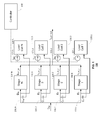
- FIG. 1 is a block diagram of a multistage circuit system 100 according to an embodiment of the present invention.
- the system 100 may include a plurality of circuit stages 110.1 - 110.N, a plurality of load cells 120.1 - 120.N, one for each circuit stage, signal lines 130.1 - 130.N, and a controller 140.
- the signal lines 130.1 - 130.N may carry synchronous data signals D 1 - D N (which may be bits of a signal D IN ) that, ideally, would be input to the circuit stages 110.1 - 110.N simultaneously with each other.
- Each signal line 130.1, ..., 130.N is input to an associated circuit stage 110.1, ..., 110.N and to an associated load cell 120.1, ..., 120.N.
- the signals D 1 - D N may be data signals, clock signals, or other signals having transitions that would be input to the circuit stages 110.1 - 110.N simultaneously with each other, notwithstanding differences in conductor length, capacitive loading, or other variations among the signal lines 130.1 - 130.N.
- the load cells 120.1 - 120.N may be tunable devices that present a variable capacitive load to the signal lines 130.1 - 130.N, shown in FIG. 1 as variable capacitors C 1 - C N .
- the load cells 120.1 - 120.N therefore, may present tunable capacitive loads to the signal lines 130.1 - 130.N that counteract effects that may cause transitions in the data signals D 1 - D N to be received out of synchronism.
- the load cells 120.1 - 120.N may have inputs coupled to the signal lines 130.1-130.N.
- Each load cell 120.1 - 120.N may include a programmable current source 121.1 - 121.N that generates a bias current I D1 - I DN through an input circuit (not shown) in a respective load stage 120.1, ..., 120.N.
- the currents I D1 - I DN flowing through each load cell 120.1 - 120.N may define the capacitive load C 1 - C N that is imposed on the signal lines 130.1 - 130.N.
- the load cells 120.1 - 120.N may have various circuit configurations.
- the load cells 120.1 - 120.N may have circuit configurations that are similar to corresponding circuit stages 110.1 - 110.N. According to other embodiments of the present invention, the load cells 120.1 - 120.N may have circuit configurations that are not similar to corresponding circuit stages 110.1 - 110.N. The configuration of the load cells 120.1 - 120.N may be unique to the multistage circuit system they are being integrated into.
- the controller 140 may be an on chip processor or state machine that stores drive strength values for the programmable current sources 121.1 - 121.N.
- the drive strength data may be derived from stored data, including estimates of signal mismatch that may be obtained, for example, from circuit simulations or test data.
- the controller 140 may include, for example, any suitable processing platform, computing platform, computing device, processing device, computing system, processing system, computer, processor, or the like, and may be implemented using any suitable combination of hardware and/or software.
- circuit stages 110.1 - 110.N are shown as driving output currents I OUT1 - I OUTN to a common output node I OUT_TOT in response to a signal D IN .
- the principles of the present invention also find application in circuit systems in which circuit stages generate output voltages in response to control signals or in which different circuit stages drive output signals, whether they be currents or voltages, to separate output nodes (e.g., analog-to-digital converters or digital-to-analog converters).
- output nodes e.g., analog-to-digital converters or digital-to-analog converters.
- the bits D 1 - D n of the signal D IN may drive the corresponding circuit stages 110.1 - 110.N during each operation, based on the value of the bits D 1 - D N .
- the circuit stages 110.1 and 110.N may be driven to output currents I OUT_1 and I OUT_N , respectively.
- the circuit stages 110.2 and 110.3 may not be driven if the bits D 2 and D 3 have a low value (in other words, I OUT_2 and I OUT_3 may be equal to 0).
- the total output current I OUT_TOT may equal I OUT_1 + I OUT_N .
- the values of D 1 - D N may vary during subsequent circuit operations, therefore, the output current I OUT_TOT may also vary for those operations.
- the current I D1 - I DN flowing through each load cell 120.1 - 120.N may provide a capacitive load on the corresponding signal lines 130.1 - 130.N to minimize timing mismatch between the output currents I OUT_1 - I OUT_N for a given circuit operation.
- the controller 140 may control the programmable current sources 121.1 and 121.N to generate the currents I D1 and I DN , respectively, based on the existing mismatch data.
- the currents I D1 and I DN flowing through the respective load cells 120.1 and 120.N may define the capacitive loads C 1 and C 4 (shown in dashed lines) that are imposed on the signal lines 130.1 and 130.N, respectively.
- the capacitive loads C 1 and C 4 provided on the signal lines D 1 and D 4 may be varied for the given operation X to allow fine timing adjustment between the circuit stages 110.1 and 110.N.
- the currents I D1 - I D4 may provide capacitive loads on the signal lines 130.1 - 130.N (depending on which bits are high and which bits are low for the operation in question) to allow fine timing adjustment between the circuit stages 110.1 - 110.N of the system 100.
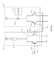
- Figures 2(a) and (b) are circuit diagrams each illustrating exemplary circuit stages and load stages according to embodiments of the present invention.
- Figure 2(a) is a block diagram of a circuit stage 210.1 and a load circuit 220.1 in a multistage circuit system according to an embodiment of the present invention.
- the load circuit 220.1 may be in parallel to the circuit stage 210.1.
- the inputs of the load circuit 220.1 and the circuit stage 210.1 may be coupled to a common signal line 115.1 that carries signal SIG IN .
- figure 2(a) only shows one circuit stage 210.1 and one load circuit 220.1
- a multistage circuit system according to embodiments of the present invention may include a plurality of circuit stages (210.1 - 210.N) and corresponding load circuits (220.1 - 220.N) in a configuration that may be similar to the multistage circuit system 100 in figure 1 .
- the circuit stage 210.1 may include an impedance 211.1 and a transistor 213.1 and.
- the transistor 213.1 may be p-type metal-oxide-semiconductor (PMOS) transistors, n-type metal-oxide-semiconductor (NMOS) transistors, or other types of transistors that are suitable for use in the circuit stage 210.1.
- the impedance 211.1 may be coupled to a voltage VDD on one end and a source terminal of the transistor 213.1 on the other end.
- a gate terminal of the transistor 213.1 may be coupled to the signal line 215.1.
- the current flowing through the impedance 211.1 may be steered by the transistor 213.1, which may act as a switch. If the signal SIG IN is high, the transistor 213.1 may be switched on, and the current flowing through the impedance 211.1 may be output to a node I OUT by the circuit stage 210.1.
- the load circuit 220.1 may include a programmable current source 221.1, a controller 222.1, and a transistor 223.1.
- the transistor 223.1 may be of a same type (PMOS, NMOS, etc.) as the transistor 213.1 in the circuit stage 210.1.
- the programmable current source 221.1 may be similar to the programmable current sources 121.1 - 121.N in figure 1 .
- the controller 222.1 may be similar to the controller 140 in figure 1 and may govern a bias current generated by the programmable current source 221.1 based on stored timing mismatch data.
- the programmable current source 221.1 may be coupled to a voltage VDD on one end and a source terminal of the transistor 223.1 on the other end.
- a gate terminal of the transistor 223.1 may be coupled to signal line 215.1 and a drain terminal of the transistor 223.1 may be coupled to ground. If the signal SIG IN is high, the transistor 223.1 may be switched on, and the current generated by the programmable current source 221.1 may flow through transistor 223.1 towards ground.
- the controller 222.1 may control the programmable current source 221.1 to generate a bias current based on the existing mismatch data.
- the bias current may flow through the transistor 223.1 toward ground and may define a gate-to-drain capacitance 214.1 (shown in dashed lines) of the transistor 213.1.
- a capacitive load 214.1 may be provided on signal line 215.1 to allow fine timing adjustment of the circuit stage 210.1.
- the controller 222.1 may vary the load presented on the signal line 215.1 by adjusting the bias current generated by the programmable current source 221.1.
- the same timing adjustment scheme may be used in the other circuit stages 210.2 - 210.N (not shown) of a multistage circuit system.
- Figure 2(b) is a block diagram of a circuit stage 230.1 and a corresponding load circuit 240.1 according to another embodiment of the present invention.
- the circuit stage 230.1 is a differential version of the circuit stage 210.1 in figure 2(a) .
- the load circuit 240.1 is a differential version of the load circuit 220.1 of figure 2(a) .
- the load circuit 240.1 may be in parallel to the circuit stage 230.1.
- a multistage circuit system may include a plurality of circuit stages (230.1 - 230.N) and corresponding load circuits (240.1 - 240.N) in a configuration that may be similar to the multistage circuit system 100 in figure 1 .
- the circuit stage 230.1 may include an impedance 231.1 and transistors 233.1 - 234.1.
- the transistors 233.1 - 234.1 may be PMOS transistors, NMOS transistors, or other types of transistors that are suitable for use in the circuit stage 230.1.
- the impedance 231.1 may be coupled to a voltage VDD on one end and source terminals of the transistors 233.1 and 234.1.
- a gate terminal of the transistor 233.1 may be coupled to a signal line 237.1 that carries a signal SIG IN1 .
- a gate terminal of the transistor 234.1 may be coupled a signal line 238.1 that carries a signal SIG IN2 .
- the transistors 233.1 and 234.1 may act as switches to steer a current flowing through the impedance 231.1. If the signal SIG IN1 is high, the transistor 233.1 may be switched on, and the current flowing through impedance 231.1 may be steered to an output I OUTP . Alternatively, if the signal SIG IN2 is high, the transistor 234.1 may be switched on, and the current flowing through the transistor 231.1 may be steered to an output I OUTN .
- the load circuit 240.1 may include a programmable current source 241.1, a controller 242.1, and a pair of transistor 243.1 and 244.1.
- the transistors 243.1 and 244.1 may be of a same type (PMOS, NMOS, etc.) as the transistors 233.1 and 234.1 in the circuit stage 230.1.
- the programmable current source 241.1 may be similar to the programmable current sources 121.1 - 121.N in figure 1 .
- the controller 242.1 may be similar to the controller 140 in figure 1 and may govern a bias current generated by the programmable current source 241.1 based on stored timing mismatch data.
- the programmable current source 241.1 may be coupled to VDD on one end and a source terminal of each transistor 243.1 and 244.1 on the other end.
- a gate terminal of the transistor 243.1 may be coupled to the signal line 2371.1 and a drain terminal of the transistor 243.1 may be coupled to ground.
- a gate terminal of the transistor 244.1 may be coupled to the signal line 238.1 and a drain terminal of the transistor 244.1 may be coupled to ground.
- the controller 242.1 may control the programmable current source 241.1 to generate a bias current based on the existing mismatch data. If the signal SIG IN1 is high, the bias current may flow through the transistor 243.1 to ground and define a gate-to-drain capacitance 235.1 (shown in dashed lines) of the transistor 233.1. Alternatively, if the signal SIG IN2 is high, the bias current may flow through the transistor 244.1 to ground and may define a gate-to-drain capacitance 236.1 (shown in dashed lines) of the transistor 234.1. In this manner, a capacitive load may be provided on the signal lines 237.1 and 238.1 to allow fine timing adjustment of the circuit stage 230.1.
- the controller 242.1 may vary the load presented on the signal lines 237.1 and 238.1 by adjusting the bias current generated by the programmable current source 241.1.
- the same adjustment scheme may be used in the other circuit stages 220.2 - 220.N (not shown) of a multistage circuit system.
- FIG. 3 is a block diagram of a multistage clock distribution circuit 300 according to an embodiment of the present invention.
- the clock distribution circuit 300 may include a plurality of buffer circuits 310.1 - 310.N, a plurality of load inverters 320.1 - 320.N, one for each buffer circuit 310.1 - 310.N, signal lines 330.1 - 330.N, and a controller 340.
- the signal lines 330.1 - 330.N may carry synchronous clock signals CLK 1 - CLK N (which represent distributed versions of the clock signal CLK that are present at each buffer 310.1 - 310.N) that, ideally, would be input to the buffers 310.1 - 310.N simultaneously with each other.
- Each signal line 330.1, ..., 330.N is input to an associated buffer 310.1, ..., 310.N and to an associated load inverter 320.1, ..., 320.N.
- the distributed clock signals CLK 1 - CLK N would be input the buffers 310.1 - 310.N simultaneously with each other, notwithstanding differences in conductor length, capacitive loading, or other variations among the signal lines 330.1- 330.N.
- the load inverters 320.1 - 320.N may be tunable devices that present a variable capacitive load to the signal lines 330.1 - 330.N, shown in FIG. 3 as variable capacitors C 1 - C N .
- the load inverters 320.1 - 320.N therefore, may present tunable capacitive loads to the signal lines 330.1 - 330.N that counteract some other effects that may cause transitions in the clock signals CLK 1 - CLK N to be received out of synchronism.
- Each buffer 310.1 - 310.N may include an inverter 312.1 - 312.N.
- the buffers 310.1 - 310.N may each receive a distributed clock signal CLK 1 - CLK N and output a corresponding buffered clock signal CLK BUFF1 - CLK BUFF4 .
- the buffered clock signals CLK BUFF1 - CLK BUFF4 may be provided to ADCs, DACs, or other components (not shown) that may be driven by a clock signal.
- the load inverters 320.1 - 320.N may have inputs coupled to the signal lines 330.1 - 330.N.
- Each load inverter 320.1 - 320.N may include a programmable current source 321.1 - 321.N that generates a bias current I D1 - I DN through an input circuit (not shown) in a respective load inverters 320.1, ..., 320.N.
- the currents I D1 - I DN flowing through each load inverter 320.1 - 320.N may define the capacitive load C 1 - C N that is imposed on the signal lines 330.1 - 330.N.
- the controller 340 may be an on chip processor or state machine that stores drive strength values for the programmable current sources 321.1 - 321.N.
- the drive strength data may be derived from stored data, including estimates of signal mismatch that may be obtained, for example, from circuit simulations or test data.
- the controller 340 may include, for example, any suitable processing platform, computing platform, computing device, processing device, computing system, processing system, computer, processor, or the like, and may be implemented using any suitable combination of hardware and/or software.
- the principles of the present invention find application with a variety of circuit systems.
- the buffers 310.1 - 310.N are shown as providing a clock signal CLK (in a distributed form) to a plurality of circuits, such as ADCs or DACs (not shown).
- CLK clock signal
- the principles of the present invention also find application in circuit systems including circuit stages that receive signals and are required to provide synchronized outputs in response to the signals. Examples of such circuits may include the embodiments described above with respect to figures 1 and 2 (as well as other systems not specifically mentioned in this discussion).
- the controller 340 may control the programmable current sources 321.1 - 321.N to generate the bias currents I D1 - I D4 , respectively, based on the existing mismatch data.
- the bias currents I D1 - I DN flowing through the respective load inverters 321.1 - 321.N may define the capacitive loads C 1 - C N (shown in dashed lines) to the signal lines 330.1 - 330.N. In this manner, a predetermined capacitive load may be provided to each signal line 330.1 - 330.N for a given clock cycle Y to allow fine timing adjustment between the buffers 310.1 - 310.N.
- the bias currents I D1 - I DN may provide capacitive loads to the signal lines 330.1 - 330.N to allow fine timing adjustment for the clock distribution circuit 300. Consequently, the buffered clock signals CLK BUFF1 - CLK BUFF4 may be aligned with respect to time.
- embodiments described above with respect to figures 1 - 3 include load circuits for each circuit stage in a multistage circuit system, other embodiments may not require such a one-to-one configuration. In order to minimize costs and conserve space on a dye, some embodiments of the present invention may only require load circuits for selected circuit stages that need to be tuned. Embodiments of the present invention may therefore be configured to meet the needs of the system they are being integrated in.
- circuit stages and the load circuits described in figures 2 and 3 are similar (e.g., similar structures and the same types of transistors), embodiments of the present invention are not limited to such configurations.
- the circuit stages and the load circuits need not be similar to each other (i.e., different circuit structures or configurations).
- the load circuits may not be similar to the circuit stages, as long as the load circuits and the circuit stages are in parallel and the load circuits include programmable current sources to vary loads presented on signal lines carrying signals that are being input into the circuit stages.
- Embodiments of the present invention provide techniques for very fine timing adjustment in the femto-second range. For example, say we have a given circuit stage in a multistage circuit system with an input transistor (similar to transistor 213.1 in fig. 2(a) ) having a width of 6.4 microns and a length of 0.08 microns. According to embodiments of the present invention, a load circuit with a corresponding input transistor (similar to transistor 223.1 in fig. 2(a) ) of a similar size (approximately 6.4 microns by 0.08 microns) may be placed in parallel to the circuit stage. Varying a current through the load circuit transistor may shift the timing of a signal (similar to SIG IN in fig.
- a load circuit with a corresponding input transistor may be placed in parallel to the circuit stage. Varying a current through the load circuit transistor may shift the timing of a signal being input to the circuit stage transistor and the load transistor by approximately 1.5 pico-seconds.
- the benefit of the described techniques is the ability to provide fine adjustment without the need to add significant circuitry or control lines. Moreover, the techniques described above are not as susceptible to noise errors as traditional timing adjustment methods.
Abstract
Description
- The present invention relates to timing adjustment in multistage circuit systems.
- Multistage circuit systems include several segments that are driven by signals. During circuit operation, a given number of segments may be driven by the signals. Ideally, the segment outputs need to be aligned with respect to time. However, with the continued increase in operating speed and desired output frequency in multistage circuits, timing related errors are the most challenging and demanding problems. These errors include phase noise on the clock signal, duty cycle distortion, and segment to segment timing mismatch.
- Timing mismatch in multistage circuits, such as converters, causes frequency and data distortion. Existing schemes for fixing timing related errors are far too invasive and susceptible to noise. Some schemes require additional circuitry and control signals on a clock signal for every segment or include overly complex adjustment circuitry for every clock line. These schemes downgrade performance by providing additional coupling paths. Other schemes involve integrating varactors on each clocked line, however, they only allow fine resolution for small voltage adjustment. Moreover, because the varactor schemes utilize voltage for timing adjustment, they are more susceptible to noise.
- The inventor therefore perceives a need in the art for improved fine timing adjustment in multistage circuits without the need for adding significant circuitry or control lines.
- According to a first aspect of the present invention there is provided an integrated circuit, comprising: a circuit system having a plurality of circuit stages to receive respective signals; and a plurality of load circuits, one provided for each circuit stage, having inputs for the signals, each load circuit having a current source, programmable independently of the other load circuits, to propagate a current through a transistor that receives the signal.
- The integrated circuit may further comprise a controller to vary the current propagated by each current source to account for timing mismatch between the circuit stages. Advantageously, the circuit stages and the load circuits are made of transistors of a common type.
- The current propagating through the transistor may alter a load on a signal line that carries the signal.
- Preferably the circuit stages and the load circuits are in an analog-to-digital converter.
- Alternatively, the circuit stages and the load circuits are in a digital-to-analog converter.
- Advantageously, the circuit stages are buffers in a clock distribution circuit that also comprises the load circuits.
- According to a second aspect of the present invention there is provided a method comprising: receiving a plurality of signals at corresponding circuit stages; providing a load circuit, in parallel to selected circuit stages, that receives a same signal at an input transistor thereof; and driving respective bias currents through the input transistors of the load circuits to counteract timing mismatch between the signals.
- The selected circuit stages and the load circuits may be made of transistors of a common type.
- Advantageously, the current propagating through the transistor alters a load on a signal line that carries the signal.
- Preferably, the selected circuit stages and the load circuits are in an analog-to-digital converter.
- Alternatively, the circuit stages and the load circuits are in a digital-to-analog converter.
- The circuit stages may be buffers in a clock distribution circuit that also comprises the load circuits.
- According to a further aspect of the present invention there is provided a system comprising: a circuit system having a plurality of circuit stages to receive respective signals; a plurality of load circuits, one for each circuit stage, having inputs for the signals, each load circuit having a unique programmable current source that propagates a current through a transistor that receives the signal; and a controller to vary the current propagated by each unique programmable current source to reduce timing mismatch between the circuit stages.
- Preferably, the circuit stages and the load circuits are made of transistors of a common type.
- Additionally, the current propagating through the transistor may alter a load on a signal line that carries the signal.
- Preferably, the circuit stages and the load circuits are in an analog-to-digital converter.
- Alternatively, the circuit stages and the load circuits are in a digital-to-analog converter.
- The circuit stages may be buffers in a clock distribution circuit that also comprises the load circuits.
- The circuit stages and the load circuits may have different circuit configurations.
-
-
Fig. 1 is a block diagram of a multistage circuit system according to an embodiment of the present invention. -
Fig. 2(a) is a block diagram of a single stage in a multistage circuit system according to an embodiment of the present invention. -
Fig. 2(b) is a block diagram of a single stage in a multistage circuit system according to an embodiment of the present invention. -
Fig. 3 is a block diagram of a clock distribution circuit according to an embodiment of the present invention. - Embodiments of the present invention may provide non-invasive techniques for adjusting timing in multistage circuit systems. A multistage circuit system according to embodiments of the present invention may include a plurality of circuit stages coupled to signal lines that carry signals. The system may also include a plurality of load circuits, one provided in for each circuit stage. The load circuits may have inputs coupled to the signal lines that carry the signals. Each load circuit may include a current source programmable independently of the other load circuits that propagates current through an input transistor in the respective load circuit that receives the signal. The current propagating through the input transistor may provide a load on the corresponding signal line, allowing fine timing adjustment for each stage.
-
Figure 1 is a block diagram of amultistage circuit system 100 according to an embodiment of the present invention. Thesystem 100 may include a plurality of circuit stages 110.1 - 110.N, a plurality of load cells 120.1 - 120.N, one for each circuit stage, signal lines 130.1 - 130.N, and acontroller 140. The signal lines 130.1 - 130.N may carry synchronous data signals D1 - DN (which may be bits of a signal DIN) that, ideally, would be input to the circuit stages 110.1 - 110.N simultaneously with each other. Each signal line 130.1, ..., 130.N is input to an associated circuit stage 110.1, ..., 110.N and to an associated load cell 120.1, ..., 120.N. - The signals D1 - DN may be data signals, clock signals, or other signals having transitions that would be input to the circuit stages 110.1 - 110.N simultaneously with each other, notwithstanding differences in conductor length, capacitive loading, or other variations among the signal lines 130.1 - 130.N. The load cells 120.1 - 120.N may be tunable devices that present a variable capacitive load to the signal lines 130.1 - 130.N, shown in
FIG. 1 as variable capacitors C1 - CN. The load cells 120.1 - 120.N, therefore, may present tunable capacitive loads to the signal lines 130.1 - 130.N that counteract effects that may cause transitions in the data signals D1 - DN to be received out of synchronism. - The load cells 120.1 - 120.N may have inputs coupled to the signal lines 130.1-130.N. Each load cell 120.1 - 120.N may include a programmable current source 121.1 - 121.N that generates a bias current ID1 - IDN through an input circuit (not shown) in a respective load stage 120.1, ..., 120.N. The currents ID1 - IDN flowing through each load cell 120.1 - 120.N may define the capacitive load C1 - CN that is imposed on the signal lines 130.1 - 130.N. The load cells 120.1 - 120.N may have various circuit configurations. According to some embodiments of the present invention, the load cells 120.1 - 120.N may have circuit configurations that are similar to corresponding circuit stages 110.1 - 110.N. According to other embodiments of the present invention, the load cells 120.1 - 120.N may have circuit configurations that are not similar to corresponding circuit stages 110.1 - 110.N. The configuration of the load cells 120.1 - 120.N may be unique to the multistage circuit system they are being integrated into.
- The
controller 140 may be an on chip processor or state machine that stores drive strength values for the programmable current sources 121.1 - 121.N. The drive strength data may be derived from stored data, including estimates of signal mismatch that may be obtained, for example, from circuit simulations or test data. Moreover, thecontroller 140 may include, for example, any suitable processing platform, computing platform, computing device, processing device, computing system, processing system, computer, processor, or the like, and may be implemented using any suitable combination of hardware and/or software. - The principles of the present invention find application with a variety of circuit systems. In the system illustrated in
FIG. 1 , the circuit stages 110.1 - 110.N are shown as driving output currents IOUT1 - IOUTN to a common output node IOUT_TOT in response to a signal DIN. However, the principles of the present invention also find application in circuit systems in which circuit stages generate output voltages in response to control signals or in which different circuit stages drive output signals, whether they be currents or voltages, to separate output nodes (e.g., analog-to-digital converters or digital-to-analog converters). In that regard, the structure and operation of the circuit stages is immaterial to the present discussion. - During operation, the bits D1 - Dn of the signal DIN may drive the corresponding circuit stages 110.1 - 110.N during each operation, based on the value of the bits D1 - DN. For example, for a given operation X of the
multistage circuit system 100, if the bits D1 and DN have a high value (1) and D2 and D3 have a low value (0), the circuit stages 110.1 and 110.N may be driven to output currents IOUT_1 and IOUT_N, respectively. The circuit stages 110.2 and 110.3 may not be driven if the bits D2 and D3 have a low value (in other words, IOUT_2 and IOUT_3 may be equal to 0). Consequently, for the operation X, the total output current IOUT_TOT may equal IOUT_1 + IOUT_N. The values of D1 - DN may vary during subsequent circuit operations, therefore, the output current IOUT_TOT may also vary for those operations. As described below, the current ID1 - IDN flowing through each load cell 120.1 - 120.N may provide a capacitive load on the corresponding signal lines 130.1 - 130.N to minimize timing mismatch between the output currents IOUT_1 - IOUT_N for a given circuit operation. - Continuing with the example above, during the given operation X (where the bits D1 and DN have a high value and the bits D2 and D3 have a low value), the
controller 140 may control the programmable current sources 121.1 and 121.N to generate the currents ID1 and IDN, respectively, based on the existing mismatch data. The currents ID1 and IDN flowing through the respective load cells 120.1 and 120.N may define the capacitive loads C1 and C4 (shown in dashed lines) that are imposed on the signal lines 130.1 and 130.N, respectively. In this manner, the capacitive loads C1 and C4 provided on the signal lines D1 and D4 may be varied for the given operation X to allow fine timing adjustment between the circuit stages 110.1 and 110.N. In a similar fashion, during subsequent operations, the currents ID1 - ID4 may provide capacitive loads on the signal lines 130.1 - 130.N (depending on which bits are high and which bits are low for the operation in question) to allow fine timing adjustment between the circuit stages 110.1 - 110.N of thesystem 100. -
Figures 2(a) and(b) are circuit diagrams each illustrating exemplary circuit stages and load stages according to embodiments of the present invention. -
Figure 2(a) is a block diagram of a circuit stage 210.1 and a load circuit 220.1 in a multistage circuit system according to an embodiment of the present invention. The load circuit 220.1 may be in parallel to the circuit stage 210.1. In other words, the inputs of the load circuit 220.1 and the circuit stage 210.1 may be coupled to a common signal line 115.1 that carries signal SIGIN. Althoughfigure 2(a) only shows one circuit stage 210.1 and one load circuit 220.1, a multistage circuit system according to embodiments of the present invention may include a plurality of circuit stages (210.1 - 210.N) and corresponding load circuits (220.1 - 220.N) in a configuration that may be similar to themultistage circuit system 100 infigure 1 . - The circuit stage 210.1 may include an impedance 211.1 and a transistor 213.1 and. The transistor 213.1 may be p-type metal-oxide-semiconductor (PMOS) transistors, n-type metal-oxide-semiconductor (NMOS) transistors, or other types of transistors that are suitable for use in the circuit stage 210.1. The impedance 211.1 may be coupled to a voltage VDD on one end and a source terminal of the transistor 213.1 on the other end. A gate terminal of the transistor 213.1 may be coupled to the signal line 215.1.
- The current flowing through the impedance 211.1 may be steered by the transistor 213.1, which may act as a switch. If the signal SIGIN is high, the transistor 213.1 may be switched on, and the current flowing through the impedance 211.1 may be output to a node IOUT by the circuit stage 210.1.
- The load circuit 220.1 may include a programmable current source 221.1, a controller 222.1, and a transistor 223.1. The transistor 223.1 may be of a same type (PMOS, NMOS, etc.) as the transistor 213.1 in the circuit stage 210.1. The programmable current source 221.1 may be similar to the programmable current sources 121.1 - 121.N in
figure 1 . The controller 222.1 may be similar to thecontroller 140 infigure 1 and may govern a bias current generated by the programmable current source 221.1 based on stored timing mismatch data. - The programmable current source 221.1 may be coupled to a voltage VDD on one end and a source terminal of the transistor 223.1 on the other end. A gate terminal of the transistor 223.1 may be coupled to signal line 215.1 and a drain terminal of the transistor 223.1 may be coupled to ground. If the signal SIGIN is high, the transistor 223.1 may be switched on, and the current generated by the programmable current source 221.1 may flow through transistor 223.1 towards ground.
- During operation, the controller 222.1 may control the programmable current source 221.1 to generate a bias current based on the existing mismatch data. When the signal SIGIN is high, the bias current may flow through the transistor 223.1 toward ground and may define a gate-to-drain capacitance 214.1 (shown in dashed lines) of the transistor 213.1. In this manner, a capacitive load 214.1 may be provided on signal line 215.1 to allow fine timing adjustment of the circuit stage 210.1. The controller 222.1 may vary the load presented on the signal line 215.1 by adjusting the bias current generated by the programmable current source 221.1. The same timing adjustment scheme may be used in the other circuit stages 210.2 - 210.N (not shown) of a multistage circuit system.
-
Figure 2(b) is a block diagram of a circuit stage 230.1 and a corresponding load circuit 240.1 according to another embodiment of the present invention. The circuit stage 230.1 is a differential version of the circuit stage 210.1 infigure 2(a) . Similarly, the load circuit 240.1 is a differential version of the load circuit 220.1 offigure 2(a) . According to this embodiment, the load circuit 240.1 may be in parallel to the circuit stage 230.1. Althoughfigure 2(b) only shows one circuit stage 230.1 and one load circuit 240.1, a multistage circuit system according to embodiments of the present invention may include a plurality of circuit stages (230.1 - 230.N) and corresponding load circuits (240.1 - 240.N) in a configuration that may be similar to themultistage circuit system 100 infigure 1 . - The circuit stage 230.1 may include an impedance 231.1 and transistors 233.1 - 234.1. The transistors 233.1 - 234.1 may be PMOS transistors, NMOS transistors, or other types of transistors that are suitable for use in the circuit stage 230.1. The impedance 231.1 may be coupled to a voltage VDD on one end and source terminals of the transistors 233.1 and 234.1. A gate terminal of the transistor 233.1 may be coupled to a signal line 237.1 that carries a signal SIGIN1. Similarly, a gate terminal of the transistor 234.1 may be coupled a signal line 238.1 that carries a signal SIGIN2.
- The transistors 233.1 and 234.1 may act as switches to steer a current flowing through the impedance 231.1. If the signal SIGIN1 is high, the transistor 233.1 may be switched on, and the current flowing through impedance 231.1 may be steered to an output IOUTP. Alternatively, if the signal SIGIN2 is high, the transistor 234.1 may be switched on, and the current flowing through the transistor 231.1 may be steered to an output IOUTN.
- The load circuit 240.1 may include a programmable current source 241.1, a controller 242.1, and a pair of transistor 243.1 and 244.1. The transistors 243.1 and 244.1 may be of a same type (PMOS, NMOS, etc.) as the transistors 233.1 and 234.1 in the circuit stage 230.1. The programmable current source 241.1 may be similar to the programmable current sources 121.1 - 121.N in
figure 1 . The controller 242.1 may be similar to thecontroller 140 infigure 1 and may govern a bias current generated by the programmable current source 241.1 based on stored timing mismatch data. - The programmable current source 241.1 may be coupled to VDD on one end and a source terminal of each transistor 243.1 and 244.1 on the other end. A gate terminal of the transistor 243.1 may be coupled to the signal line 2371.1 and a drain terminal of the transistor 243.1 may be coupled to ground. Similarly, a gate terminal of the transistor 244.1 may be coupled to the signal line 238.1 and a drain terminal of the transistor 244.1 may be coupled to ground.
- During operation, the controller 242.1 may control the programmable current source 241.1 to generate a bias current based on the existing mismatch data. If the signal SIGIN1 is high, the bias current may flow through the transistor 243.1 to ground and define a gate-to-drain capacitance 235.1 (shown in dashed lines) of the transistor 233.1. Alternatively, if the signal SIGIN2 is high, the bias current may flow through the transistor 244.1 to ground and may define a gate-to-drain capacitance 236.1 (shown in dashed lines) of the transistor 234.1. In this manner, a capacitive load may be provided on the signal lines 237.1 and 238.1 to allow fine timing adjustment of the circuit stage 230.1. The controller 242.1 may vary the load presented on the signal lines 237.1 and 238.1 by adjusting the bias current generated by the programmable current source 241.1. The same adjustment scheme may be used in the other circuit stages 220.2 - 220.N (not shown) of a multistage circuit system.
-
Figure 3 is a block diagram of a multistage clock distribution circuit 300 according to an embodiment of the present invention. The clock distribution circuit 300 may include a plurality of buffer circuits 310.1 - 310.N, a plurality of load inverters 320.1 - 320.N, one for each buffer circuit 310.1 - 310.N, signal lines 330.1 - 330.N, and acontroller 340. The signal lines 330.1 - 330.N may carry synchronous clock signals CLK1 - CLKN (which represent distributed versions of the clock signal CLK that are present at each buffer 310.1 - 310.N) that, ideally, would be input to the buffers 310.1 - 310.N simultaneously with each other. Each signal line 330.1, ..., 330.N is input to an associated buffer 310.1, ..., 310.N and to an associated load inverter 320.1, ..., 320.N. - Ideally, the distributed clock signals CLK1 - CLKN would be input the buffers 310.1 - 310.N simultaneously with each other, notwithstanding differences in conductor length, capacitive loading, or other variations among the signal lines 330.1- 330.N. The load inverters 320.1 - 320.N may be tunable devices that present a variable capacitive load to the signal lines 330.1 - 330.N, shown in
FIG. 3 as variable capacitors C1 - CN. The load inverters 320.1 - 320.N, therefore, may present tunable capacitive loads to the signal lines 330.1 - 330.N that counteract some other effects that may cause transitions in the clock signals CLK1 - CLKN to be received out of synchronism. - Each buffer 310.1 - 310.N may include an inverter 312.1 - 312.N. The buffers 310.1 - 310.N may each receive a distributed clock signal CLK1 - CLKN and output a corresponding buffered clock signal CLKBUFF1 - CLKBUFF4. According to embodiments of the present invention, the buffered clock signals CLKBUFF1 - CLKBUFF4 may be provided to ADCs, DACs, or other components (not shown) that may be driven by a clock signal.
- The load inverters 320.1 - 320.N may have inputs coupled to the signal lines 330.1 - 330.N. Each load inverter 320.1 - 320.N may include a programmable current source 321.1 - 321.N that generates a bias current ID1 - IDN through an input circuit (not shown) in a respective load inverters 320.1, ..., 320.N. The currents ID1 - IDN flowing through each load inverter 320.1 - 320.N may define the capacitive load C1 - CN that is imposed on the signal lines 330.1 - 330.N.
- The
controller 340 may be an on chip processor or state machine that stores drive strength values for the programmable current sources 321.1 - 321.N. The drive strength data may be derived from stored data, including estimates of signal mismatch that may be obtained, for example, from circuit simulations or test data. Moreover, thecontroller 340 may include, for example, any suitable processing platform, computing platform, computing device, processing device, computing system, processing system, computer, processor, or the like, and may be implemented using any suitable combination of hardware and/or software. - The principles of the present invention find application with a variety of circuit systems. In the system 300 illustrated in
FIG. 3 , the buffers 310.1 - 310.N are shown as providing a clock signal CLK (in a distributed form) to a plurality of circuits, such as ADCs or DACs (not shown). However, the principles of the present invention also find application in circuit systems including circuit stages that receive signals and are required to provide synchronized outputs in response to the signals. Examples of such circuits may include the embodiments described above with respect tofigures 1 and2 (as well as other systems not specifically mentioned in this discussion). - During a given clock cycle Y, the
controller 340 may control the programmable current sources 321.1 - 321.N to generate the bias currents ID1 - ID4, respectively, based on the existing mismatch data. The bias currents ID1 - IDN flowing through the respective load inverters 321.1 - 321.N may define the capacitive loads C1 - CN (shown in dashed lines) to the signal lines 330.1 - 330.N. In this manner, a predetermined capacitive load may be provided to each signal line 330.1 - 330.N for a given clock cycle Y to allow fine timing adjustment between the buffers 310.1 - 310.N. In a similar fashion, during subsequent clock cycles, the bias currents ID1 - IDN may provide capacitive loads to the signal lines 330.1 - 330.N to allow fine timing adjustment for the clock distribution circuit 300. Consequently, the buffered clock signals CLKBUFF1 - CLKBUFF4 may be aligned with respect to time. - Although the embodiments described above with respect to
figures 1 - 3 include load circuits for each circuit stage in a multistage circuit system, other embodiments may not require such a one-to-one configuration. In order to minimize costs and conserve space on a dye, some embodiments of the present invention may only require load circuits for selected circuit stages that need to be tuned. Embodiments of the present invention may therefore be configured to meet the needs of the system they are being integrated in. - Moreover, although the circuit stages and the load circuits described in
figures 2 and3 are similar (e.g., similar structures and the same types of transistors), embodiments of the present invention are not limited to such configurations. The circuit stages and the load circuits need not be similar to each other (i.e., different circuit structures or configurations). According to other embodiments of the present invention, the load circuits may not be similar to the circuit stages, as long as the load circuits and the circuit stages are in parallel and the load circuits include programmable current sources to vary loads presented on signal lines carrying signals that are being input into the circuit stages. - Embodiments of the present invention provide techniques for very fine timing adjustment in the femto-second range. For example, say we have a given circuit stage in a multistage circuit system with an input transistor (similar to transistor 213.1 in
fig. 2(a) ) having a width of 6.4 microns and a length of 0.08 microns. According to embodiments of the present invention, a load circuit with a corresponding input transistor (similar to transistor 223.1 infig. 2(a) ) of a similar size (approximately 6.4 microns by 0.08 microns) may be placed in parallel to the circuit stage. Varying a current through the load circuit transistor may shift the timing of a signal (similar to SIGIN infig. 2(a) ) being input to the circuit stage transistor and the load transistor by approximately 400 femto-seconds. Similarly, say we have a given circuit stage in a multistage circuit system with an input transistor having a width of 1.6 microns and a length of 0.08 microns. According to embodiments of the present invention, a load circuit with a corresponding input transistor, having a length of 11.2 microns and a width 0.08 microns, may be placed in parallel to the circuit stage. Varying a current through the load circuit transistor may shift the timing of a signal being input to the circuit stage transistor and the load transistor by approximately 1.5 pico-seconds. - The benefit of the described techniques is the ability to provide fine adjustment without the need to add significant circuitry or control lines. Moreover, the techniques described above are not as susceptible to noise errors as traditional timing adjustment methods.
- Although the foregoing techniques have been described above with reference to specific embodiments, the invention is not limited to the above embodiments and the specific configurations shown in the drawings. For example, some components shown may be combined with each other as one embodiment, or a component may be divided into several subcomponents, or any other known or available component may be added. Those skilled in the art will appreciate that these techniques may be implemented in other ways without departing from the spirit and substantive features of the invention. The present embodiments are therefore to be considered in all respects as illustrative and not restrictive.
Claims (14)
- An integrated circuit, comprising:a circuit system having a plurality of circuit stages to receive respective signals; anda plurality of load circuits, one provided for each circuit stage, having inputs for the signals, each load circuit having a current source, programmable independently of the other load circuits, to propagate a current through a transistor that receives the signal.
- The circuit of claim 1, further comprising a controller to vary the current propagated by each current source to account for timing mismatch between the circuit stages.
- The circuit of claim 1 or 2, wherein the circuit stages and the load circuits are made of transistors of a common type.
- The circuit of any preceding claim, wherein the current propagating through the transistor alters a load on a signal line that carries the signal.
- The circuit of any preceding claim, in which at least one of the following applies:a) the circuit stages and the load circuits are in an analog-to-digital converter;b) the circuit stages and the load circuits are in a digital-to-analog converter;c) the circuit stages are buffers in a clock distribution circuit that also comprises the load circuits.
- A method comprising:receiving a plurality of signals at corresponding circuit stages;providing a load circuit, in parallel to selected circuit stages, that receives a same signal at an input transistor thereof; anddriving respective bias currents through the input transistors of the load circuits to counteract timing mismatch between the signals.
- The method of claim 6, wherein the selected circuit stages and the load circuits are made of transistors of a common type.
- The method of claim 6 or 7, wherein the current propagating through the transistor alters a load on a signal line that carries the signal.
- The method of any one of claims 6 to 8, in whihc at least one of the following applies:a) the selected circuit stages and the load circuits are in an analog-to-digital converter;b) the circuit stages and the load circuits are in a digital-to-analog converter;c) the circuit stages are buffers in a clock distribution circuit that also comprises the load circuits.
- A system comprising:a circuit system having a plurality of circuit stages to receive respective signals;a plurality of load circuits, one for each circuit stage, having inputs for the signals, each load circuit having a unique programmable current source that propagatesa current through a transistor that receives the signal; anda controller to vary the current propagated by each unique programmable current source to reduce timing mismatch between the circuit stages.
- The system of claim 10, wherein the circuit stages and the load circuits are made of transistors of a common type.
- The system of claim 10 or 11, wherein the current propagating through the transistor alters a load on a signal line that carries the signal.
- The system of any one of claims 10 to 12, in which at least one of the following applies:a) the circuit stages and the load circuits are in an analog-to-digital converter;b) the circuit stages and the load circuits are in a digital-to-analog converter;c) the circuit stages are buffers in a clock distribution circuit that also comprises the load circuits.
- The system of any one of claims 10 to 12, wherein the circuit stages and the load circuits have different circuit configurations.
Applications Claiming Priority (1)
| Application Number | Priority Date | Filing Date | Title |
|---|---|---|---|
| US13/829,889 US9887552B2 (en) | 2013-03-14 | 2013-03-14 | Fine timing adjustment method |
Publications (3)
| Publication Number | Publication Date |
|---|---|
| EP2779460A2 true EP2779460A2 (en) | 2014-09-17 |
| EP2779460A3 EP2779460A3 (en) | 2015-12-23 |
| EP2779460B1 EP2779460B1 (en) | 2021-02-24 |
Family
ID=50389782
Family Applications (1)
| Application Number | Title | Priority Date | Filing Date |
|---|---|---|---|
| EP14157771.8A Active EP2779460B1 (en) | 2013-03-14 | 2014-03-05 | Fine timing adjustment method |
Country Status (4)
| Country | Link |
|---|---|
| US (1) | US9887552B2 (en) |
| EP (1) | EP2779460B1 (en) |
| CN (1) | CN104052437B (en) |
| ES (1) | ES2864130T3 (en) |
Families Citing this family (1)
| Publication number | Priority date | Publication date | Assignee | Title |
|---|---|---|---|---|
| JP2015008025A (en) * | 2013-06-25 | 2015-01-15 | マイクロン テクノロジー, インク. | Semiconductor device |
Family Cites Families (30)
| Publication number | Priority date | Publication date | Assignee | Title |
|---|---|---|---|---|
| US5663241A (en) * | 1994-12-13 | 1997-09-02 | Minnesota Mining And Manufacturing Company | Removable pressure sensitive adhesive and article |
| JP4090088B2 (en) * | 1996-09-17 | 2008-05-28 | 富士通株式会社 | Semiconductor device system and semiconductor device |
| US5945863A (en) * | 1997-06-18 | 1999-08-31 | Applied Micro Circuits Corporation | Analog delay circuit |
| JPH11203866A (en) * | 1998-01-16 | 1999-07-30 | Mitsubishi Electric Corp | Semiconductor storage device |
| JP3271610B2 (en) * | 1999-04-05 | 2002-04-02 | 日本電気株式会社 | Semiconductor device |
| US6194962B1 (en) * | 1999-04-13 | 2001-02-27 | Analog Devices, Inc. | Adaptive operational amplifier offset voltage trimming system |
| US6530062B1 (en) * | 2000-03-10 | 2003-03-04 | Rambus Inc. | Active impedance compensation |
| TW536066U (en) * | 2001-03-13 | 2003-06-01 | Realtek Semiconductor Corp | Impedance matching circuit |
| US6617926B2 (en) * | 2001-06-29 | 2003-09-09 | Intel Corporation | Tail current node equalization for a variable offset amplifier |
| US6614371B2 (en) * | 2001-07-19 | 2003-09-02 | Broadcom Corporation | Synchronous data serialization circuit |
| US6535534B1 (en) * | 2001-09-10 | 2003-03-18 | Agere Systems Inc. | Optical source driver with bias circuit for controlling output overshoot |
| US6501314B1 (en) * | 2002-03-06 | 2002-12-31 | Teradyne, Inc. | Programmable differential D flip-flop |
| US8064508B1 (en) * | 2002-09-19 | 2011-11-22 | Silicon Image, Inc. | Equalizer with controllably weighted parallel high pass and low pass filters and receiver including such an equalizer |
| US6831516B2 (en) * | 2003-02-20 | 2004-12-14 | Semiconductor Components Industries, L.L.C. | Method of forming a variable propagation delay semiconductor device and structure therefor |
| US6819155B1 (en) * | 2003-06-23 | 2004-11-16 | Teradyne, Inc. | High-speed duty cycle control circuit |
| US6919833B2 (en) * | 2003-09-04 | 2005-07-19 | Regan N. Mills | Parallel converter topology for reducing non-linearity errors |
| US7049889B2 (en) * | 2004-03-31 | 2006-05-23 | Analog Devices, Inc. | Differential stage voltage offset trim circuitry |
| US7193468B2 (en) * | 2004-05-14 | 2007-03-20 | Electronics And Telecommunications Research Institute | Active load circuit for low-voltage CMOS voltage gain amplifier with wide bandwidth and high gain characteristic |
| US7466200B2 (en) * | 2004-10-06 | 2008-12-16 | Agere Systems Inc. | Composite output stage for hard disk drive preamplifier |
| US7071858B2 (en) * | 2004-10-29 | 2006-07-04 | Broadcom Corporation | Method and system for a glitch-free differential current steering switch circuit for high speed, high resolution digital-to-analog conversion |
| KR100644273B1 (en) * | 2004-12-21 | 2006-11-10 | 한국전자통신연구원 | Low noise amplifier of wide-band tunable matching |
| US20060238235A1 (en) * | 2005-01-19 | 2006-10-26 | James Wey | Switchable current mirror with feedback |
| US7532065B2 (en) * | 2005-07-12 | 2009-05-12 | Agere Systems Inc. | Analog amplifier having DC offset cancellation circuit and method of offset cancellation for analog amplifiers |
| US7720015B2 (en) * | 2005-08-17 | 2010-05-18 | Teranetics, Inc. | Receiver ADC clock delay base on echo signals |
| US7598788B2 (en) * | 2005-09-06 | 2009-10-06 | Broadcom Corporation | Current-controlled CMOS (C3MOS) fully differential integrated delay cell with variable delay and high bandwidth |
| US7545194B2 (en) * | 2006-06-30 | 2009-06-09 | Intel Corporation | Programmable delay for clock phase error correction |
| US7425909B2 (en) * | 2006-07-31 | 2008-09-16 | Analog Devices, Inc. | Low-noise programmable current source |
| US7668153B2 (en) * | 2007-03-27 | 2010-02-23 | Adc Telecommunications, Inc. | Method for data converter sample clock distribution |
| US8536944B2 (en) * | 2011-02-15 | 2013-09-17 | Cavium, Inc. | Differential amplifier with de-emphasis |
| US9306509B2 (en) * | 2012-07-27 | 2016-04-05 | Xilinx, Inc. | Receiver having a wide common mode input range |
-
2013
- 2013-03-14 US US13/829,889 patent/US9887552B2/en active Active
-
2014
- 2014-03-05 EP EP14157771.8A patent/EP2779460B1/en active Active
- 2014-03-05 ES ES14157771T patent/ES2864130T3/en active Active
- 2014-03-14 CN CN201410093892.4A patent/CN104052437B/en active Active
Non-Patent Citations (1)
| Title |
|---|
| None |
Also Published As
| Publication number | Publication date |
|---|---|
| CN104052437A (en) | 2014-09-17 |
| US9887552B2 (en) | 2018-02-06 |
| EP2779460B1 (en) | 2021-02-24 |
| ES2864130T3 (en) | 2021-10-13 |
| CN104052437B (en) | 2018-03-13 |
| EP2779460A3 (en) | 2015-12-23 |
| US20140265578A1 (en) | 2014-09-18 |
Similar Documents
| Publication | Publication Date | Title |
|---|---|---|
| US8552783B2 (en) | Programmable delay generator and cascaded interpolator | |
| EP2352228A1 (en) | Comparator and analog/digital converter | |
| US20190163231A1 (en) | Semiconductor integrated circuit, and method for supplying clock signals in semiconductor integrated circuit | |
| US7649957B2 (en) | Non-overlapping multi-stage clock generator system | |
| US7956785B2 (en) | Return to zero digital to analog converter and converting method thereof | |
| KR101038470B1 (en) | Digital controlled oscillator with wide dynamic range | |
| US20130207698A1 (en) | Clock distribution system and method for a multi-bit latch | |
| US20110037511A1 (en) | Multiple signal switching circuit, current switching cell circuit, latch circuit, current steering type dac, semiconductor integrated circuit, video device, and communication device | |
| US6617909B2 (en) | Phase blender and multi-phase generator using the same | |
| JP2019215881A (en) | Semiconductor integrated circuit and clock supply method for semiconductor integrated circuit | |
| US10367506B1 (en) | Digital circuit based on a modified tristate circuit | |
| US9419636B1 (en) | Clocked current-steering circuit for a digital-to-analog converter | |
| US10135600B2 (en) | Multiplexers | |
| EP2779460B1 (en) | Fine timing adjustment method | |
| KR100691108B1 (en) | Delay chain capable of reducing skew between input and output signals | |
| US8830101B1 (en) | Single phase clock D/A converter with built-in data combiner | |
| JP2012234088A (en) | Driving circuit and display device with the same | |
| US20130176151A1 (en) | Serializer | |
| US9712182B1 (en) | Digital to analog conversion circuit and method | |
| JP6075191B2 (en) | Interpolation circuit and reception circuit | |
| EP1903678A2 (en) | Sequence independent non-overlapping digital signal generator with programmable delay | |
| US7969224B2 (en) | Circuit to reduce duty cycle distortion | |
| US9201813B2 (en) | Signal distribution circuitry | |
| JP2017207857A (en) | Signal multiplexing device | |
| US8994408B2 (en) | Electronic circuit |
Legal Events
| Date | Code | Title | Description |
|---|---|---|---|
| PUAI | Public reference made under article 153(3) epc to a published international application that has entered the european phase |
Free format text: ORIGINAL CODE: 0009012 |
|
| 17P | Request for examination filed |
Effective date: 20140305 |
|
| AK | Designated contracting states |
Kind code of ref document: A2 Designated state(s): AL AT BE BG CH CY CZ DE DK EE ES FI FR GB GR HR HU IE IS IT LI LT LU LV MC MK MT NL NO PL PT RO RS SE SI SK SM TR |
|
| AX | Request for extension of the european patent |
Extension state: BA ME |
|
| PUAL | Search report despatched |
Free format text: ORIGINAL CODE: 0009013 |
|
| AK | Designated contracting states |
Kind code of ref document: A3 Designated state(s): AL AT BE BG CH CY CZ DE DK EE ES FI FR GB GR HR HU IE IS IT LI LT LU LV MC MK MT NL NO PL PT RO RS SE SI SK SM TR |
|
| AX | Request for extension of the european patent |
Extension state: BA ME |
|
| RIC1 | Information provided on ipc code assigned before grant |
Ipc: H03M 1/10 20060101AFI20151117BHEP Ipc: H03M 1/74 20060101ALN20151117BHEP Ipc: H03M 1/66 20060101ALN20151117BHEP Ipc: H03M 1/12 20060101ALN20151117BHEP |
|
| R17P | Request for examination filed (corrected) |
Effective date: 20160621 |
|
| RBV | Designated contracting states (corrected) |
Designated state(s): AL AT BE BG CH CY CZ DE DK EE ES FI FR GB GR HR HU IE IS IT LI LT LU LV MC MK MT NL NO PL PT RO RS SE SI SK SM TR |
|
| STAA | Information on the status of an ep patent application or granted ep patent |
Free format text: STATUS: EXAMINATION IS IN PROGRESS |
|
| 17Q | First examination report despatched |
Effective date: 20180123 |
|
| RIC1 | Information provided on ipc code assigned before grant |
Ipc: H03M 1/66 20060101ALN20200630BHEP Ipc: H03M 1/10 20060101AFI20200630BHEP Ipc: H03M 1/12 20060101ALN20200630BHEP Ipc: H03M 1/74 20060101ALN20200630BHEP |
|
| REG | Reference to a national code |
Ref country code: DE Ref legal event code: R079 Ref document number: 602014075061 Country of ref document: DE Free format text: PREVIOUS MAIN CLASS: H03M0001060000 Ipc: H03M0001100000 |
|
| GRAP | Despatch of communication of intention to grant a patent |
Free format text: ORIGINAL CODE: EPIDOSNIGR1 |
|
| STAA | Information on the status of an ep patent application or granted ep patent |
Free format text: STATUS: GRANT OF PATENT IS INTENDED |
|
| RIC1 | Information provided on ipc code assigned before grant |
Ipc: H03M 1/66 20060101ALN20200827BHEP Ipc: H03M 1/12 20060101ALN20200827BHEP Ipc: H03M 1/74 20060101ALN20200827BHEP Ipc: H03M 1/10 20060101AFI20200827BHEP |
|
| INTG | Intention to grant announced |
Effective date: 20200911 |
|
| RIC1 | Information provided on ipc code assigned before grant |
Ipc: H03M 1/66 20060101ALN20200828BHEP Ipc: H03M 1/10 20060101AFI20200828BHEP Ipc: H03M 1/12 20060101ALN20200828BHEP Ipc: H03M 1/74 20060101ALN20200828BHEP |
|
| GRAS | Grant fee paid |
Free format text: ORIGINAL CODE: EPIDOSNIGR3 |
|
| GRAA | (expected) grant |
Free format text: ORIGINAL CODE: 0009210 |
|
| STAA | Information on the status of an ep patent application or granted ep patent |
Free format text: STATUS: THE PATENT HAS BEEN GRANTED |
|
| AK | Designated contracting states |
Kind code of ref document: B1 Designated state(s): AL AT BE BG CH CY CZ DE DK EE ES FI FR GB GR HR HU IE IS IT LI LT LU LV MC MK MT NL NO PL PT RO RS SE SI SK SM TR |
|
| REG | Reference to a national code |
Ref country code: GB Ref legal event code: FG4D |
|
| REG | Reference to a national code |
Ref country code: CH Ref legal event code: EP |
|
| REG | Reference to a national code |
Ref country code: DE Ref legal event code: R096 Ref document number: 602014075061 Country of ref document: DE |
|
| REG | Reference to a national code |
Ref country code: AT Ref legal event code: REF Ref document number: 1365781 Country of ref document: AT Kind code of ref document: T Effective date: 20210315 |
|
| REG | Reference to a national code |
Ref country code: IE Ref legal event code: FG4D |
|
| REG | Reference to a national code |
Ref country code: FI Ref legal event code: FGE |
|
| REG | Reference to a national code |
Ref country code: SE Ref legal event code: TRGR |
|
| REG | Reference to a national code |
Ref country code: LT Ref legal event code: MG9D |
|
| REG | Reference to a national code |
Ref country code: NL Ref legal event code: MP Effective date: 20210224 |
|
| PG25 | Lapsed in a contracting state [announced via postgrant information from national office to epo] |
Ref country code: GR Free format text: LAPSE BECAUSE OF FAILURE TO SUBMIT A TRANSLATION OF THE DESCRIPTION OR TO PAY THE FEE WITHIN THE PRESCRIBED TIME-LIMIT Effective date: 20210525 Ref country code: HR Free format text: LAPSE BECAUSE OF FAILURE TO SUBMIT A TRANSLATION OF THE DESCRIPTION OR TO PAY THE FEE WITHIN THE PRESCRIBED TIME-LIMIT Effective date: 20210224 Ref country code: PT Free format text: LAPSE BECAUSE OF FAILURE TO SUBMIT A TRANSLATION OF THE DESCRIPTION OR TO PAY THE FEE WITHIN THE PRESCRIBED TIME-LIMIT Effective date: 20210624 Ref country code: LT Free format text: LAPSE BECAUSE OF FAILURE TO SUBMIT A TRANSLATION OF THE DESCRIPTION OR TO PAY THE FEE WITHIN THE PRESCRIBED TIME-LIMIT Effective date: 20210224 Ref country code: BG Free format text: LAPSE BECAUSE OF FAILURE TO SUBMIT A TRANSLATION OF THE DESCRIPTION OR TO PAY THE FEE WITHIN THE PRESCRIBED TIME-LIMIT Effective date: 20210524 Ref country code: NO Free format text: LAPSE BECAUSE OF FAILURE TO SUBMIT A TRANSLATION OF THE DESCRIPTION OR TO PAY THE FEE WITHIN THE PRESCRIBED TIME-LIMIT Effective date: 20210524 |
|
| REG | Reference to a national code |
Ref country code: AT Ref legal event code: MK05 Ref document number: 1365781 Country of ref document: AT Kind code of ref document: T Effective date: 20210224 |
|
| RAP4 | Party data changed (patent owner data changed or rights of a patent transferred) |
Owner name: ANALOG DEVICES, INC. |
|
| PG25 | Lapsed in a contracting state [announced via postgrant information from national office to epo] |
Ref country code: RS Free format text: LAPSE BECAUSE OF FAILURE TO SUBMIT A TRANSLATION OF THE DESCRIPTION OR TO PAY THE FEE WITHIN THE PRESCRIBED TIME-LIMIT Effective date: 20210224 Ref country code: NL Free format text: LAPSE BECAUSE OF FAILURE TO SUBMIT A TRANSLATION OF THE DESCRIPTION OR TO PAY THE FEE WITHIN THE PRESCRIBED TIME-LIMIT Effective date: 20210224 Ref country code: LV Free format text: LAPSE BECAUSE OF FAILURE TO SUBMIT A TRANSLATION OF THE DESCRIPTION OR TO PAY THE FEE WITHIN THE PRESCRIBED TIME-LIMIT Effective date: 20210224 Ref country code: PL Free format text: LAPSE BECAUSE OF FAILURE TO SUBMIT A TRANSLATION OF THE DESCRIPTION OR TO PAY THE FEE WITHIN THE PRESCRIBED TIME-LIMIT Effective date: 20210224 |
|
| PG25 | Lapsed in a contracting state [announced via postgrant information from national office to epo] |
Ref country code: IS Free format text: LAPSE BECAUSE OF FAILURE TO SUBMIT A TRANSLATION OF THE DESCRIPTION OR TO PAY THE FEE WITHIN THE PRESCRIBED TIME-LIMIT Effective date: 20210624 |
|
| REG | Reference to a national code |
Ref country code: ES Ref legal event code: FG2A Ref document number: 2864130 Country of ref document: ES Kind code of ref document: T3 Effective date: 20211013 |
|
| PG25 | Lapsed in a contracting state [announced via postgrant information from national office to epo] |
Ref country code: SM Free format text: LAPSE BECAUSE OF FAILURE TO SUBMIT A TRANSLATION OF THE DESCRIPTION OR TO PAY THE FEE WITHIN THE PRESCRIBED TIME-LIMIT Effective date: 20210224 Ref country code: EE Free format text: LAPSE BECAUSE OF FAILURE TO SUBMIT A TRANSLATION OF THE DESCRIPTION OR TO PAY THE FEE WITHIN THE PRESCRIBED TIME-LIMIT Effective date: 20210224 Ref country code: CZ Free format text: LAPSE BECAUSE OF FAILURE TO SUBMIT A TRANSLATION OF THE DESCRIPTION OR TO PAY THE FEE WITHIN THE PRESCRIBED TIME-LIMIT Effective date: 20210224 Ref country code: AT Free format text: LAPSE BECAUSE OF FAILURE TO SUBMIT A TRANSLATION OF THE DESCRIPTION OR TO PAY THE FEE WITHIN THE PRESCRIBED TIME-LIMIT Effective date: 20210224 |
|
| REG | Reference to a national code |
Ref country code: CH Ref legal event code: PL |
|
| REG | Reference to a national code |
Ref country code: DE Ref legal event code: R097 Ref document number: 602014075061 Country of ref document: DE |
|
| PG25 | Lapsed in a contracting state [announced via postgrant information from national office to epo] |
Ref country code: MC Free format text: LAPSE BECAUSE OF FAILURE TO SUBMIT A TRANSLATION OF THE DESCRIPTION OR TO PAY THE FEE WITHIN THE PRESCRIBED TIME-LIMIT Effective date: 20210224 Ref country code: DK Free format text: LAPSE BECAUSE OF FAILURE TO SUBMIT A TRANSLATION OF THE DESCRIPTION OR TO PAY THE FEE WITHIN THE PRESCRIBED TIME-LIMIT Effective date: 20210224 Ref country code: RO Free format text: LAPSE BECAUSE OF FAILURE TO SUBMIT A TRANSLATION OF THE DESCRIPTION OR TO PAY THE FEE WITHIN THE PRESCRIBED TIME-LIMIT Effective date: 20210224 Ref country code: SK Free format text: LAPSE BECAUSE OF FAILURE TO SUBMIT A TRANSLATION OF THE DESCRIPTION OR TO PAY THE FEE WITHIN THE PRESCRIBED TIME-LIMIT Effective date: 20210224 |
|
| REG | Reference to a national code |
Ref country code: BE Ref legal event code: MM Effective date: 20210331 |
|
| PLBE | No opposition filed within time limit |
Free format text: ORIGINAL CODE: 0009261 |
|
| STAA | Information on the status of an ep patent application or granted ep patent |
Free format text: STATUS: NO OPPOSITION FILED WITHIN TIME LIMIT |
|
| PG25 | Lapsed in a contracting state [announced via postgrant information from national office to epo] |
Ref country code: IE Free format text: LAPSE BECAUSE OF NON-PAYMENT OF DUE FEES Effective date: 20210305 Ref country code: LI Free format text: LAPSE BECAUSE OF NON-PAYMENT OF DUE FEES Effective date: 20210331 Ref country code: LU Free format text: LAPSE BECAUSE OF NON-PAYMENT OF DUE FEES Effective date: 20210305 Ref country code: CH Free format text: LAPSE BECAUSE OF NON-PAYMENT OF DUE FEES Effective date: 20210331 Ref country code: AL Free format text: LAPSE BECAUSE OF FAILURE TO SUBMIT A TRANSLATION OF THE DESCRIPTION OR TO PAY THE FEE WITHIN THE PRESCRIBED TIME-LIMIT Effective date: 20210224 |
|
| 26N | No opposition filed |
Effective date: 20211125 |
|
| REG | Reference to a national code |
Ref country code: DE Ref legal event code: R081 Ref document number: 602014075061 Country of ref document: DE Owner name: ANALOG DEVICES, INC., WILMINGTON, US Free format text: FORMER OWNER: ANALOG DEVICES, INC., NORWOOD, MASS., US |
|
| PG25 | Lapsed in a contracting state [announced via postgrant information from national office to epo] |
Ref country code: SI Free format text: LAPSE BECAUSE OF FAILURE TO SUBMIT A TRANSLATION OF THE DESCRIPTION OR TO PAY THE FEE WITHIN THE PRESCRIBED TIME-LIMIT Effective date: 20210224 |
|
| PG25 | Lapsed in a contracting state [announced via postgrant information from national office to epo] |
Ref country code: IS Free format text: LAPSE BECAUSE OF FAILURE TO SUBMIT A TRANSLATION OF THE DESCRIPTION OR TO PAY THE FEE WITHIN THE PRESCRIBED TIME-LIMIT Effective date: 20210624 |
|
| PGFP | Annual fee paid to national office [announced via postgrant information from national office to epo] |
Ref country code: IT Payment date: 20220217 Year of fee payment: 9 |
|
| PG25 | Lapsed in a contracting state [announced via postgrant information from national office to epo] |
Ref country code: BE Free format text: LAPSE BECAUSE OF NON-PAYMENT OF DUE FEES Effective date: 20210331 |
|
| PGFP | Annual fee paid to national office [announced via postgrant information from national office to epo] |
Ref country code: FR Payment date: 20230222 Year of fee payment: 10 Ref country code: FI Payment date: 20230223 Year of fee payment: 10 |
|
| PG25 | Lapsed in a contracting state [announced via postgrant information from national office to epo] |
Ref country code: HU Free format text: LAPSE BECAUSE OF FAILURE TO SUBMIT A TRANSLATION OF THE DESCRIPTION OR TO PAY THE FEE WITHIN THE PRESCRIBED TIME-LIMIT; INVALID AB INITIO Effective date: 20140305 |
|
| PGFP | Annual fee paid to national office [announced via postgrant information from national office to epo] |
Ref country code: SE Payment date: 20230222 Year of fee payment: 10 Ref country code: GB Payment date: 20230221 Year of fee payment: 10 Ref country code: DE Payment date: 20230221 Year of fee payment: 10 |
|
| PG25 | Lapsed in a contracting state [announced via postgrant information from national office to epo] |
Ref country code: CY Free format text: LAPSE BECAUSE OF FAILURE TO SUBMIT A TRANSLATION OF THE DESCRIPTION OR TO PAY THE FEE WITHIN THE PRESCRIBED TIME-LIMIT Effective date: 20210224 |
|
| PGFP | Annual fee paid to national office [announced via postgrant information from national office to epo] |
Ref country code: ES Payment date: 20230403 Year of fee payment: 10 |