EP2777093B1 - Directional slot antenna with a dielectric insert - Google Patents
Directional slot antenna with a dielectric insert Download PDFInfo
- Publication number
- EP2777093B1 EP2777093B1 EP12847616.5A EP12847616A EP2777093B1 EP 2777093 B1 EP2777093 B1 EP 2777093B1 EP 12847616 A EP12847616 A EP 12847616A EP 2777093 B1 EP2777093 B1 EP 2777093B1
- Authority
- EP
- European Patent Office
- Prior art keywords
- reflector
- antenna
- dielectric material
- spacing cavity
- reflector spacing
- Prior art date
- Legal status (The legal status is an assumption and is not a legal conclusion. Google has not performed a legal analysis and makes no representation as to the accuracy of the status listed.)
- Active
Links
Images

Classifications
-
- H—ELECTRICITY
- H01—ELECTRIC ELEMENTS
- H01Q—ANTENNAS, i.e. RADIO AERIALS
- H01Q13/00—Waveguide horns or mouths; Slot antennas; Leaky-waveguide antennas; Equivalent structures causing radiation along the transmission path of a guided wave
- H01Q13/10—Resonant slot antennas
- H01Q13/18—Resonant slot antennas the slot being backed by, or formed in boundary wall of, a resonant cavity ; Open cavity antennas
-
- H—ELECTRICITY
- H01—ELECTRIC ELEMENTS
- H01Q—ANTENNAS, i.e. RADIO AERIALS
- H01Q1/00—Details of, or arrangements associated with, antennas
- H01Q1/36—Structural form of radiating elements, e.g. cone, spiral, umbrella; Particular materials used therewith
- H01Q1/38—Structural form of radiating elements, e.g. cone, spiral, umbrella; Particular materials used therewith formed by a conductive layer on an insulating support
-
- H—ELECTRICITY
- H01—ELECTRIC ELEMENTS
- H01Q—ANTENNAS, i.e. RADIO AERIALS
- H01Q13/00—Waveguide horns or mouths; Slot antennas; Leaky-waveguide antennas; Equivalent structures causing radiation along the transmission path of a guided wave
- H01Q13/10—Resonant slot antennas
- H01Q13/106—Microstrip slot antennas
-
- H—ELECTRICITY
- H01—ELECTRIC ELEMENTS
- H01Q—ANTENNAS, i.e. RADIO AERIALS
- H01Q19/00—Combinations of primary active antenna elements and units with secondary devices, e.g. with quasi-optical devices, for giving the antenna a desired directional characteristic
- H01Q19/10—Combinations of primary active antenna elements and units with secondary devices, e.g. with quasi-optical devices, for giving the antenna a desired directional characteristic using reflecting surfaces
-
- H—ELECTRICITY
- H01—ELECTRIC ELEMENTS
- H01Q—ANTENNAS, i.e. RADIO AERIALS
- H01Q21/00—Antenna arrays or systems
- H01Q21/24—Combinations of antenna units polarised in different directions for transmitting or receiving circularly and elliptically polarised waves or waves linearly polarised in any direction
Definitions
- the present invention relates generally to antennas, and, more particularly, to directional antennas with gaps between radiating components and reflectors.
- GNSS receivers use antennas to receive GNSS signals, such as L1, L2, and L5 signals, transmitted by GNSS satellites.
- GNSS signals such as L1, L2, and L5 signals
- One example of such an antenna is described in commonly owned U.S. Patent No. 6,445,354 by Kunysz issued on September 3, 2002 entitled, APERTURE COUPLED SLOT ARRAY ANTENNA.
- the antenna which radiates in both directions along its axis, may be made directional by the inclusion of a reflector that is strategically placed relative to the radiating component of the antenna.
- the directional slot antenna may be made from a printed circuit board (PCB) with a second PCB placed underneath and spaced from the antenna to act as a reflector to provide the antenna directivity and also to reduce back-lobe radiation.
- PCB printed circuit board
- Directional slot array antennas which include directional pinwheel (PW) antennas, are designed with a reflector spacing between the radiating component of the antenna and the reflector.
- the reflector spacing height is related to the signal frequency or frequencies of interest and a desired gain. For example, to satisfy gain requirements at L1 and L2, the height of the reflector spacing is typically 15mm. To satisfy the gain requirements at the lower frequency L5, the reflector spacing height needs to be larger, typically between 17 and 19mm.
- US 3 717 877 A discloses a cavity backed spiral antenna, where antenna elements are mounted upon a sheet of ferrite material.
- the sheet has a geometrical shape such that it fits the interior of a cavity and serves to provide a loading of the equiangular spiral antenna elements.
- the antenna elements combined with the ferrite sheet fill the entire space of the cavity to produce a functioning radiating component.
- US 2010/141542 A1 describes an antenna utilizing a conductive reference sheet where each side of the sheet includes a dielectric material having specific K values.
- US 7 250 916 B2 describes a leaky wave antenna with a radiating structure including fractal loops.
- the antenna substrate has a radiating slot structure on an upper surface thereof, where a cavity is formed between a ground plane and a lower surface.
- US 7 250 916 B2 describes the ground plane associated with a working antenna.
- a disadvantage of prior directional PW antennas is that as the reflector spacing height is increased to satisfy desired gain requirements at lower frequencies, such as the L5 band, the overall size of the antenna necessarily increases. Enlarging the antenna to receive the L5 signals may require altering the configurations of devices that utilize the antenna. Further, consumer demand is typically for smaller electronic devices.
- an antenna that is capable of receiving lower frequency signals, such as L5 signals, that have dimensions similar or equal to the dimensions of an antenna that receives higher frequency signals such as L1 and L2. Additionally, there is a need for a smaller antenna that is capable of receiving the higher frequency signals, such as L1 and L2 signals.
- a directional slot antenna comprises a radiating component coupled to a reflector, a reflector spacing gap or cavity between the radiating component and the reflector, and a dielectric insert within the reflector spacing reflector spacing cavity.
- the reflector spacing cavity height is less than a predetermined height of a free-space reflector spacing cavity associated with desired gains for the one or more frequencies of interest.
- the dielectric material insert positioned within the reflector spacing cavity partially fills the reflector spacing cavity vertically, and the combination of the dielectric material insert and the remaining unfilled portion of the reflector spacing cavity provides an electrical separation between the radiating component and the reflector that corresponds to the predetermined height of the free- space reflector spacing cavity.
- the directional slot antenna, with the reduced-height reflector spacing cavity is thus compact while maintaining desired gain performance across the frequencies of interest, e.g., the Global Navigation Satellite System (GNSS) L1, L2, and L5 frequencies.
- GNSS Global Navigation Satellite System
- the antenna 10 has a radiating component 20 comprised of a conductive layer 12 that includes a plurality of similar curved, slotted openings 14, 16, 18, and 20. Each slotted opening 14, 16, 18, and 20 extends through the conductive layer 12 to the front surface 22 of a substrate 24 of nonconductive or dielectric material having a thickness t.
- a transmission line 26 is disposed on an opposite side 32 of the substrate 24.
- the antenna 10 may thus be fabricated from a two-layer printed circuit board (PCB), where the transmission line 26 and the slotted openings 14, 16, 18, and 20 can be formed by suitably etching portions of the respective cladding layers.
- PCB printed circuit board
- the present invention is not limited to this number and may comprise m slotted openings of varying shapes and lengths, where m > 2 .
- electromagnetic energy radiated by the radiating component 20 is emitted in both directions along the antenna axis 11.
- a reflector 42 is emplaced in opposed parallel relationship to the back surface 32 of the antenna 10 and separated by a reflector spacing gap or cavity 50.
- the separation between the back surface 32 and the reflector has a vertical free-space reflector spacing height g, which is needed to satisfy desired gain requirements at the frequencies of interest.
- An antenna designed to receive L1 and L2 signals, for example, has a vertical reflector spacing height of approximately 15mm.
- An RF foam absorber 28 which may be an additional PCB layer, vertically spans the outer diameter of the cavity 50 to reduce leakage of cross-polarized signals from the directional antenna.
- the slotted openings can be curved in shape as shown, or can be straight segments or a combination of both straight and curved segments, as described in greater detail below.
- the curved shapes can be a conical section (i.e., a circular, elliptical, parabolic, or hyperbolic arc), an Archimedean spiral, a logarithmic spiral, or an exponential spiral.
- fractal loops described by Kunysz et al., in U.S. Patent No.
- Straight slotted openings are equivalent to dipoles and, as such, a single slotted opening produces a linearly polarized signal.
- an array of straight slotted openings can be used to transmit, or receive, a circularly-polarized signal, as can be appreciated by those skilled in the art.
- Circular polarization can also be produced by using an array of curved slotted openings, where the respective slotted openings are curved in the direction of the desired circular polarization (i.e., a clockwise curvature to receive or transmit left-hand circularly polarized signals).
- the slotted openings 14, 16, 18, and 20 have respective axial ends proximate the antenna axis 11, and respective peripheral ends proximate the peripheral edge 30.
- the respective axial ends of the respective slotted opening lie inside the circle defined by the transmission line 26 on the opposite side of the substrate 24. Accordingly, when the antenna 10 is used to transmit signals, electromagnetic energy is fed into the transmission line 26 and is electromagnetically coupled to the slotted opening 14, 16, 18, and 20. This coupling occurs at the four respective regions where the slotted openings 14, 16, 18, and 20 which lie on the front surface, are located most proximate to and directly opposite the transmission line 26 which lies on the back surface 32 of the planar antenna 10.
- a portion of the slotted opening 14 is located a distance equivalent to the substrate thickness t from the transmission line 26 at a coupling region 34.
- the electromagnetic energy passing through transmission line 26 will produce a radiating field across the slotted opening 14 in the coupling region 34.
- This electromagnetic energy will be similarly coupled into slotted openings 16, 18, and 20 at coupling regions 36, 38, and 39 respectively.
- the degree of coupling is a function of the thickness t of the substrate 24, the width w of the transmission line 26, the width v of the slotted opening 14, and the dielectric properties of the substrate 24.
- the antenna 10 when the antenna 10 is used to receive signals, radiation energy is received at the slotted openings 14, 16, 18, and 20 is coupled into the transmission line 26 at the respective coupling regions 34, 36, 38, and 39. While a single spiral transmission line is shown in the drawing, the transmission line may have multiple spirals that cross the slots multiple times, as discussed in the above noted Patent No. 7,250,916 .
- the radiation pattern emitted from the antenna 10, as well as the radiation pattern roll-off characteristics and other characteristics, such as impedance, can be varied as desired by increasing or decreasing the separation, i.e., height of the free-space reflector spacing cavity 50, between the reflector 42 and the radiating component 20.
- the free-space reflector spacing height g is illustratively 15mm.
- the free-space reflector spacing height needs to be greater, typically between 17 and 19mm.
- an increase in the reflector spacing height required to satisfy desired gain requirements (and other performance requirements) for lower frequencies increases the overall size of the antenna.
- the antenna comprises the radiating component 20 discussed above with reference to Fig. 1 , and thus includes the conductive layer 12 with the slots, the dielectric or nonconductive substrate 24, and the transmission line 26.
- the reflector 42 is emplaced in opposed parallel relationship to the back surface 32 of the radiating component 20, and a reflector spacing gap or cavity 500 of height g' ⁇ g separates the reflector and the radiating component.
- a dielectric material insert 44 illustratively made of a ceramic is positioned on the reflector 42 and partially fills the vertical dimension of the reflector spacing cavity 500.
- the RF foam absorber 280 utilized in the antenna 100 has a horizontal thickness, e.g., 7-12mm, that is measured inwardly from an outer edge of the antenna and thus spans only a portion of the reflector spacing cavity 500 in the horizontal direction.
- the RF foam absorber 280 has a vertical dimension that is reduced from that of the RF foam absorber 28 of antenna 10 in accordance with the reduction in the height of the reflector spacing cavity 500.
- the dielectric material insert 44 is situated inside the foam absorber, with the outer diameter of the dielectric material insert 44 touching the inner diameter of the absorber. It should be noted that when the entire reflector spacing cavity 500 is not filled vertically by the dielectric material insert, an air gap remains, in particular, under the transmission line 26, to maintain appropriate impedance values.
- the antennas 10 and 100 of Figs. 2 and 3 are each designed for L1, L2 and L5 signals.
- the antenna 100 includes the dielectric material insert 44, which in the example is a ceramic disk 3.5mm in height, within the reflector spacing cavity 500, such that the reflector spacing is partially filled by the insert 44.
- the overall height of the reflector spacing cavity 500 is thus reduced in the example to g' ⁇ 8- 10mm, which is even less than the free-space reflector spacing cavity height associated with the L1 and L2 signals.
- the vertical thickness of the dielectric material plus any remaining unfilled vertical portion of the reflector spacing cavity is equal to a height of g', which is less than the predetermined height of the free-space reflector spacing vertical cavity height g.
- the combination maintains the overall performance of the antenna 100 across the GNSS frequencies, with the antenna 100 also capable of receiving L5 signals at the desired gains.
- the insert 44 may be dimensioned to further reduce the reflector spacing cavity 500 below that required for reception of the L1 and L2 signals alone, while the antenna also operates as desired at the L5 frequency.
- Fig. 4 is a perspective view of the antenna 100.
- the vertical height of absorber 280 coupled to substrate 24 is greater than the vertical height of the dielectric material insert 44.
- the dielectric material insert 44 is shaped as a disk or ring with the placement of the material corresponding to the location of the slots and a center hole 45 corresponding to the location of the transmission line, to reduce the overall weight of the antenna.
- insert 44 may be utilized in an antenna 100 designed for use with only L1 and L2 signals to reduce the height of the reflector spacing cavity 500 below the 15mm height of the free-space reflector spacing cavity 50.
- the thickness of the dielectric material insert 44 as discussed is 3.5mm, those skilled in the art will appreciate that the thickness as well as other dimensions of the insert may vary depending upon the specific antenna merits desired. Thus, any specific dimensions described should be taken as exemplary only and not to otherwise limit the scope of the invention. Furthermore, those skilled in the art will recognize that alternative design choices may be made to change the dimensions of the antenna while maintaining desired antenna characteristics. For example, different thicknesses of the dielectric material insert and/or different permittivities may be utilized to reduce the height of the reflector spacing cavity 500 by greater or lesser amounts, even by as much as 50% or more for L1, L2, and L5.
- the present invention may be used with other signals/frequencies, such as Galileo E1, E2 and E5 and Glonass G1 and G2. As such, any description of specific frequencies should be taken as exemplary only and not to otherwise limit the scope of the invention. Further, the RF foam absorber 280 may be omitted.
- the dielectric insert may be used depending upon the location of the active radiating area, whereby the dielectric material is between the active radiating portions of the radiating component, i.e., the slots and the reflector.
- the embodiments of the invention in their broader sense are not so limited, and may, in fact, be used with radio broadcasting, broadcast television, two-way radio, communications receivers, radar, cell phones, as well as other devices such as garage door openers, wireless microphones, Bluetooth enabled devices, wireless computer networks, etc. using any appropriate frequency. Additionally, while embodiments have been shown and described in terms of a pinwheel antenna design, those skilled in the art will appreciate that non-pinwheel designs may also be used.
- dielectric material insert 44 may be made from materials other than ceramic and/or materials with other levels of permittivity.
Landscapes
- Aerials With Secondary Devices (AREA)
- Waveguide Aerials (AREA)
- Variable-Direction Aerials And Aerial Arrays (AREA)
- Details Of Aerials (AREA)
Description
- The present invention relates generally to antennas, and, more particularly, to directional antennas with gaps between radiating components and reflectors.
- Global Navigation Satellite System (GNSS) receivers use antennas to receive GNSS signals, such as L1, L2, and L5 signals, transmitted by GNSS satellites. One example of such an antenna is described in commonly owned
U.S. Patent No. 6,445,354 by Kunysz issued on September 3, 2002 entitled, APERTURE COUPLED SLOT ARRAY ANTENNA. The antenna, which radiates in both directions along its axis, may be made directional by the inclusion of a reflector that is strategically placed relative to the radiating component of the antenna. The directional slot antenna may be made from a printed circuit board (PCB) with a second PCB placed underneath and spaced from the antenna to act as a reflector to provide the antenna directivity and also to reduce back-lobe radiation. - Directional slot array antennas, which include directional pinwheel (PW) antennas, are designed with a reflector spacing between the radiating component of the antenna and the reflector. The reflector spacing height is related to the signal frequency or frequencies of interest and a desired gain. For example, to satisfy gain requirements at L1 and L2, the height of the reflector spacing is typically 15mm. To satisfy the gain requirements at the lower frequency L5, the reflector spacing height needs to be larger, typically between 17 and 19mm.
-
US 3 717 877 A discloses a cavity backed spiral antenna, where antenna elements are mounted upon a sheet of ferrite material. The sheet has a geometrical shape such that it fits the interior of a cavity and serves to provide a loading of the equiangular spiral antenna elements. Thus, the antenna elements combined with the ferrite sheet fill the entire space of the cavity to produce a functioning radiating component. -
US 2010/141542 A1 describes an antenna utilizing a conductive reference sheet where each side of the sheet includes a dielectric material having specific K values. -
US 7 250 916 B2 describes a leaky wave antenna with a radiating structure including fractal loops. The antenna substrate has a radiating slot structure on an upper surface thereof, where a cavity is formed between a ground plane and a lower surface. Thus,US 7 250 916 B2 describes the ground plane associated with a working antenna. - Volakis J. L. et al: "A Broadband Cavity-Backed Slot Spiral Antenna", IEEE ANTENNAS AND PROPAGATION MAGAZINE, IEEE SERVICE CENTER, PISCATAWAY, NJ, US, vol. 43, no. 6, pages 15-26 describe a broadband cavity-backed slot spiral antenna having a reflector cavity, wherein the size of the reflector cavity is a function of a slot width and a substrate dielectric constant.
- A disadvantage of prior directional PW antennas is that as the reflector spacing height is increased to satisfy desired gain requirements at lower frequencies, such as the L5 band, the overall size of the antenna necessarily increases. Enlarging the antenna to receive the L5 signals may require altering the configurations of devices that utilize the antenna. Further, consumer demand is typically for smaller electronic devices.
- Accordingly, there is a need for an antenna that is capable of receiving lower frequency signals, such as L5 signals, that have dimensions similar or equal to the dimensions of an antenna that receives higher frequency signals such as L1 and L2. Additionally, there is a need for a smaller antenna that is capable of receiving the higher frequency signals, such as L1 and L2 signals.
- The invention is defined by the independent claim 1. Optional features are set-out by the dependent claims.
- A directional slot antenna comprises a radiating component coupled to a reflector, a reflector spacing gap or cavity between the radiating component and the reflector, and a dielectric insert within the reflector spacing reflector spacing cavity. The reflector spacing cavity height is less than a predetermined height of a free-space reflector spacing cavity associated with desired gains for the one or more frequencies of interest. The dielectric material insert positioned within the reflector spacing cavity partially fills the reflector spacing cavity vertically, and the combination of the dielectric material insert and the remaining unfilled portion of the reflector spacing cavity provides an electrical separation between the radiating component and the reflector that corresponds to the predetermined height of the free- space reflector spacing cavity. The directional slot antenna, with the reduced-height reflector spacing cavity, is thus compact while maintaining desired gain performance across the frequencies of interest, e.g., the Global Navigation Satellite System (GNSS) L1, L2, and L5 frequencies.
- The above and further advantages of the invention may be better understood by referring to the following description in conjunction with the accompanying drawings in which like reference numerals indicate identically or functionally similar elements, of which:
-
Fig. 1 is a view of the top of a prior art slot antenna showing an array of slotted openings disposed in the conductive plane; -
Fig. 2 is a side view of the antenna ofFig. 1 showing placement of a reflector; -
Fig. 3 is a side view of a slot antenna constructed in accordance with the invention; and -
Fig. 4 is a more detailed view of a reflector and associated dielectric insert ofFig. 3 . - A known
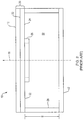
directional slot antenna 10 is discussed with reference toFigs. 1-2 , and the improveddirectional slot antenna 100 is discussed below with reference toFigs. 3-4 . Referring toFigs. 1 and2 , theantenna 10 has a radiatingcomponent 20 comprised of aconductive layer 12 that includes a plurality of similar curved, slottedopenings opening conductive layer 12 to thefront surface 22 of asubstrate 24 of nonconductive or dielectric material having a thickness t. Atransmission line 26 is disposed on anopposite side 32 of thesubstrate 24. Theantenna 10 may thus be fabricated from a two-layer printed circuit board (PCB), where thetransmission line 26 and theslotted openings - As can be appreciated by one skilled in the relevant art, electromagnetic energy radiated by the
radiating component 20 is emitted in both directions along theantenna axis 11. To provide directionality, and thus, increase the proportion of energy emitted in the forward direction and also to reduce the back-lobe radiation, areflector 42 is emplaced in opposed parallel relationship to theback surface 32 of theantenna 10 and separated by a reflector spacing gap orcavity 50. Illustratively, the separation between theback surface 32 and the reflector has a vertical free-space reflector spacing height g, which is needed to satisfy desired gain requirements at the frequencies of interest. An antenna designed to receive L1 and L2 signals, for example, has a vertical reflector spacing height of approximately 15mm. An RF foam absorber 28, which may be an additional PCB layer, vertically spans the outer diameter of thecavity 50 to reduce leakage of cross-polarized signals from the directional antenna. As is known, the slotted openings can be curved in shape as shown, or can be straight segments or a combination of both straight and curved segments, as described in greater detail below. The curved shapes can be a conical section (i.e., a circular, elliptical, parabolic, or hyperbolic arc), an Archimedean spiral, a logarithmic spiral, or an exponential spiral. Those skilled in the art will recognize that other slot antenna configurations may be utilized, such as fractal loops, described byKunysz et al., in U.S. Patent No. 7,250,916 issued on July 31, 2007 . Straight slotted openings are equivalent to dipoles and, as such, a single slotted opening produces a linearly polarized signal. However, an array of straight slotted openings can be used to transmit, or receive, a circularly-polarized signal, as can be appreciated by those skilled in the art. Circular polarization can also be produced by using an array of curved slotted openings, where the respective slotted openings are curved in the direction of the desired circular polarization (i.e., a clockwise curvature to receive or transmit left-hand circularly polarized signals). By using curved slotted openings having the equivalent guided wave lengths of straight slotted openings, the physical size of the antenna can be reduced. - The
slotted openings antenna axis 11, and respective peripheral ends proximate the peripheral edge 30. The respective axial ends of the respective slotted opening lie inside the circle defined by thetransmission line 26 on the opposite side of thesubstrate 24. Accordingly, when theantenna 10 is used to transmit signals, electromagnetic energy is fed into thetransmission line 26 and is electromagnetically coupled to theslotted opening slotted openings transmission line 26 which lies on theback surface 32 of theplanar antenna 10. - For example, a portion of the slotted
opening 14 is located a distance equivalent to the substrate thickness t from thetransmission line 26 at acoupling region 34. As is well known in the art, the electromagnetic energy passing throughtransmission line 26 will produce a radiating field across theslotted opening 14 in thecoupling region 34. This electromagnetic energy will be similarly coupled into slottedopenings coupling regions substrate 24, the width w of thetransmission line 26, the width v of theslotted opening 14, and the dielectric properties of thesubstrate 24. Conversely, when theantenna 10 is used to receive signals, radiation energy is received at the slottedopenings transmission line 26 at therespective coupling regions 7,250,916 - As is also known in the art, the radiation pattern emitted from the
antenna 10, as well as the radiation pattern roll-off characteristics and other characteristics, such as impedance, can be varied as desired by increasing or decreasing the separation, i.e., height of the free-spacereflector spacing cavity 50, between thereflector 42 and the radiatingcomponent 20. For example, to satisfy the gain requirements at L1 and L2, the free-space reflector spacing height g is illustratively 15mm. To also satisfy the same gain requirements at the lower frequency L5, the free-space reflector spacing height needs to be greater, typically between 17 and 19mm. As can be appreciated, an increase in the reflector spacing height required to satisfy desired gain requirements (and other performance requirements) for lower frequencies, increases the overall size of the antenna. - Referring now to
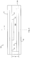
Fig. 3 , animproved antenna 100 is depicted. The antenna comprises the radiatingcomponent 20 discussed above with reference toFig. 1 , and thus includes theconductive layer 12 with the slots, the dielectric ornonconductive substrate 24, and thetransmission line 26. Thereflector 42 is emplaced in opposed parallel relationship to theback surface 32 of the radiatingcomponent 20, and a reflector spacing gap orcavity 500 of height g' < g separates the reflector and the radiating component. Adielectric material insert 44 illustratively made of a ceramic is positioned on thereflector 42 and partially fills the vertical dimension of thereflector spacing cavity 500. - Electromagnetic waves propagate slower in a high permittivity dielectric material than in free-space. Accordingly, including the
insert 44 in thereflector spacing cavity 500 provides an increased electrical separation between the radiatingcomponent 20 and thereflector 42 without requiring an increase in the physical separation of the free-space reflector spacing cavity. Rather, the overall height of the reflector spacing with the includedinsert 44 can be reduced to g' < g without adversely affecting the performance of the antenna, that is, without changing the antenna merits from those achieved with an reflector spacing having the free-space reflector spacing height g. - The
RF foam absorber 280 utilized in theantenna 100 has a horizontal thickness, e.g., 7-12mm, that is measured inwardly from an outer edge of the antenna and thus spans only a portion of thereflector spacing cavity 500 in the horizontal direction. Notably, theRF foam absorber 280 has a vertical dimension that is reduced from that of theRF foam absorber 28 ofantenna 10 in accordance with the reduction in the height of thereflector spacing cavity 500. Thedielectric material insert 44 is situated inside the foam absorber, with the outer diameter of thedielectric material insert 44 touching the inner diameter of the absorber. It should be noted that when the entirereflector spacing cavity 500 is not filled vertically by the dielectric material insert, an air gap remains, in particular, under thetransmission line 26, to maintain appropriate impedance values. - As an example, the
antennas Figs. 2 and3 are each designed for L1, L2 and L5 signals. Theantenna 10 has a free-spacereflector spacing cavity 50, which has a height g = 17- 19mm that satisfies desired gain requirements at the frequencies of interest. Theantenna 100 includes thedielectric material insert 44, which in the example is a ceramic disk 3.5mm in height, within thereflector spacing cavity 500, such that the reflector spacing is partially filled by theinsert 44. The overall height of thereflector spacing cavity 500 is thus reduced in the example to g' ∼ 8- 10mm, which is even less than the free-space reflector spacing cavity height associated with the L1 and L2 signals. - The vertical thickness of the dielectric material plus any remaining unfilled vertical portion of the reflector spacing cavity is equal to a height of g', which is less than the predetermined height of the free-space reflector spacing vertical cavity height g. However, the combination maintains the overall performance of the
antenna 100 across the GNSS frequencies, with theantenna 100 also capable of receiving L5 signals at the desired gains. As desired, theinsert 44 may be dimensioned to further reduce thereflector spacing cavity 500 below that required for reception of the L1 and L2 signals alone, while the antenna also operates as desired at the L5 frequency. -
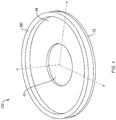
Fig. 4 is a perspective view of theantenna 100. In the illustrative embodiment, the vertical height ofabsorber 280 coupled to substrate 24 (not shown) is greater than the vertical height of thedielectric material insert 44. Those skilled in the art will appreciate that different sizes, shapes, and placements may be used depending upon the location of the active radiated area, whereby the dielectric material is placed under the active radiating portion of the radiating component, i.e., the slots. As shown inFig. 4 , thedielectric material insert 44 is shaped as a disk or ring with the placement of the material corresponding to the location of the slots and acenter hole 45 corresponding to the location of the transmission line, to reduce the overall weight of the antenna. - Further, the
insert 44 may be utilized in anantenna 100 designed for use with only L1 and L2 signals to reduce the height of thereflector spacing cavity 500 below the 15mm height of the free-spacereflector spacing cavity 50. - While the vertical thickness of the
dielectric material insert 44 as discussed is 3.5mm, those skilled in the art will appreciate that the thickness as well as other dimensions of the insert may vary depending upon the specific antenna merits desired. Thus, any specific dimensions described should be taken as exemplary only and not to otherwise limit the scope of the invention. Furthermore, those skilled in the art will recognize that alternative design choices may be made to change the dimensions of the antenna while maintaining desired antenna characteristics. For example, different thicknesses of the dielectric material insert and/or different permittivities may be utilized to reduce the height of thereflector spacing cavity 500 by greater or lesser amounts, even by as much as 50% or more for L1, L2, and L5. Moreover, while the disclosure is discussed in terms of L1, L2, and L5, those skilled in the art will recognize that the present invention may be used with other signals/frequencies, such as Galileo E1, E2 and E5 and Glonass G1 and G2. As such, any description of specific frequencies should be taken as exemplary only and not to otherwise limit the scope of the invention. Further, theRF foam absorber 280 may be omitted. - As discussed above, those skilled in the art will also appreciate that different sizes, shapes, and placements of the dielectric insert may be used depending upon the location of the active radiating area, whereby the dielectric material is between the active radiating portions of the radiating component, i.e., the slots and the reflector.
- While there have been shown and described illustrative embodiments that are used for satellite communication and GNSS frequencies, it is to be understood that various other adaptations and modifications may be made within the scope of the present invention.
- That is, the embodiments of the invention in their broader sense are not so limited, and may, in fact, be used with radio broadcasting, broadcast television, two-way radio, communications receivers, radar, cell phones, as well as other devices such as garage door openers, wireless microphones, Bluetooth enabled devices, wireless computer networks, etc. using any appropriate frequency. Additionally, while embodiments have been shown and described in terms of a pinwheel antenna design, those skilled in the art will appreciate that non-pinwheel designs may also be used.
- Those skilled in the art will also recognize that the
dielectric material insert 44 may be made from materials other than ceramic and/or materials with other levels of permittivity. - The foregoing description has been directed to specific embodiments of this invention. It will be apparent, however, other variations, equivalent substitutions, and modifications may be made to the described embodiments, including embodiment(s) taken singly or in any combination, with the attainment of some or all of their advantages. For instance, while embodiments are described in terms of a pinwheel antenna, those skilled in the art will appreciate that other antenna designs may also be used. Accordingly, this description is to be taken only by way of example and not to otherwise limit the scope of the invention. Therefore, it is the object of the appended claims to cover all such combinations, variations, and modifications as come within the scope of the invention.
Claims (4)
- A directional slot antenna (100), comprising:a radiating component (20), including a conductive layer (12) located on a first surface of a substrate (24), configured to operate as a slot antenna and to radiate electromagnetic energy in both directions along an antenna axis (11);a transmission line (26), located on a second surface of the substrate (24), configured to be electromagnetically coupled to the radiating component (20) such that the directional slot antenna (100) operates to transmit signals and receive signals, the transmission line being a spiral transmission line;a reflector (42) electrically separated from the radiating component, the reflector emplaced in opposed parallel relationship to a back surface (32) of the radiating component (20), the reflector providing directionality by reflecting the radiated electromagnetic energy emitted in the direction of the reflector (42);a reflector spacing cavity (500) between the radiating component (20) and the reflector (42), the reflector spacing cavity having a height g';a dielectric material insert (44) positioned within the reflector spacing cavity (500), the dielectric material insert (44) being placed on top of the reflector (42) and partially filling the vertical dimension of the reflector spacing cavity (500) such that an unfilled vertical portion of the reflector spacing cavity (500) remains, and the dielectric material insert (44) being shaped as a disk or ring,
with the placement of the dielectric material corresponding to a location of an active radiating portion of the radiating component, and
with a center hole corresponding to a location of the transmission line; andthe reflector spacing cavity (500) including the dielectric material (44) insert providing an increased electrical separation between the radiating component (20) and the reflector (42) and the reflector spacing cavity (500) including the dielectric material (44) producing desired gains at frequencies of interest that are the same as the desired gains at the same frequencies produced by a free-space reflector spacing cavity (50) having a height g>g'. - The antenna of claim 1, wherein the dielectric material insert comprises a permittivity dielectric material such that electromagnetic waves propagate slower in the permittivity dielectric material than in the free-space reflector spacing cavity.
- The antenna of claim 1, wherein the frequencies of interest are GNSS frequencies that comprise at least one of L1, L2, L5, Galileo E1, Galileo E5, Galileo E6, Glonass G1, Glonass G2, and Glonass G3.
- The antenna of claim 1, wherein the height g' of the reflector spacing cavity is at least 50% less than the predetermined height g of the free-space reflector spacing cavity.
Applications Claiming Priority (2)
| Application Number | Priority Date | Filing Date | Title |
|---|---|---|---|
| US13/290,532 US8797222B2 (en) | 2011-11-07 | 2011-11-07 | Directional slot antenna with a dielectric insert |
| PCT/CA2012/050787 WO2013067638A1 (en) | 2011-11-07 | 2012-11-06 | Directional slot antenna with a dielectric insert |
Publications (3)
| Publication Number | Publication Date |
|---|---|
| EP2777093A1 EP2777093A1 (en) | 2014-09-17 |
| EP2777093A4 EP2777093A4 (en) | 2015-05-06 |
| EP2777093B1 true EP2777093B1 (en) | 2019-01-09 |
Family
ID=48223344
Family Applications (1)
| Application Number | Title | Priority Date | Filing Date |
|---|---|---|---|
| EP12847616.5A Active EP2777093B1 (en) | 2011-11-07 | 2012-11-06 | Directional slot antenna with a dielectric insert |
Country Status (6)
| Country | Link |
|---|---|
| US (1) | US8797222B2 (en) |
| EP (1) | EP2777093B1 (en) |
| CN (1) | CN103975484B (en) |
| AU (1) | AU2012334771B2 (en) |
| CA (1) | CA2852360C (en) |
| WO (1) | WO2013067638A1 (en) |
Families Citing this family (10)
| Publication number | Priority date | Publication date | Assignee | Title |
|---|---|---|---|---|
| US9098352B2 (en) * | 2013-07-17 | 2015-08-04 | Deja Vu Security, Llc | Metaphor based language fuzzing of computer code |
| US10170823B2 (en) * | 2016-04-27 | 2019-01-01 | Topcon Positioning Systems, Inc. | Embedded antenna device for GNSS applications |
| CN106299626A (en) * | 2016-10-08 | 2017-01-04 | 京信通信技术(广州)有限公司 | A kind of antenna element and antenna for base station |
| US11133580B2 (en) * | 2017-06-22 | 2021-09-28 | Innolux Corporation | Antenna device |
| US11233310B2 (en) * | 2018-01-29 | 2022-01-25 | The Boeing Company | Low-profile conformal antenna |
| DE102018218253A1 (en) * | 2018-10-25 | 2020-04-30 | Robert Bosch Gmbh | Radar sensor |
| US20200227816A1 (en) * | 2019-01-11 | 2020-07-16 | Mediatek Inc. | Antenna system and associated radiated module |
| US11276933B2 (en) | 2019-11-06 | 2022-03-15 | The Boeing Company | High-gain antenna with cavity between feed line and ground plane |
| CN113161735B (en) * | 2021-04-02 | 2024-05-17 | 福耀玻璃工业集团股份有限公司 | Be applied to on-vehicle location antenna and vehicle glass |
| US12562495B2 (en) | 2023-09-08 | 2026-02-24 | KYOCERA AVX Components (San Diego), Inc. | Antenna assembly |
Citations (3)
| Publication number | Priority date | Publication date | Assignee | Title |
|---|---|---|---|---|
| US3381371A (en) * | 1965-09-27 | 1968-05-07 | Sanders Associates Inc | Method of constructing lightweight antenna |
| DE3134081A1 (en) * | 1981-08-28 | 1983-03-10 | Licentia Patent-Verwaltungs-Gmbh, 6000 Frankfurt | Spiral antenna |
| JPS6179305A (en) * | 1984-09-27 | 1986-04-22 | Tech Res & Dev Inst Of Japan Def Agency | Spiral antenna |
Family Cites Families (16)
| Publication number | Priority date | Publication date | Assignee | Title |
|---|---|---|---|---|
| US3717877A (en) * | 1970-02-27 | 1973-02-20 | Sanders Associates Inc | Cavity backed spiral antenna |
| GB2157500B (en) * | 1984-04-11 | 1987-07-01 | Plessey Co Plc | Microwave antenna |
| US5313216A (en) * | 1991-05-03 | 1994-05-17 | Georgia Tech Research Corporation | Multioctave microstrip antenna |
| SE468873B (en) | 1991-08-12 | 1993-03-29 | Nobeltech Electronics Ab | CAVITY ANTENNA WITH DIELECTRICUM |
| US5861019A (en) * | 1997-07-25 | 1999-01-19 | Medtronic Inc. | Implantable medical device microstrip telemetry antenna |
| US6160522A (en) * | 1998-04-02 | 2000-12-12 | L3 Communications Corporation, Randtron Antenna Systems Division | Cavity-backed slot antenna |
| US6445354B1 (en) | 1999-08-16 | 2002-09-03 | Novatel, Inc. | Aperture coupled slot array antenna |
| US6518930B2 (en) * | 2000-06-02 | 2003-02-11 | The Regents Of The University Of California | Low-profile cavity-backed slot antenna using a uniplanar compact photonic band-gap substrate |
| US6642898B2 (en) | 2001-05-15 | 2003-11-04 | Raytheon Company | Fractal cross slot antenna |
| US6836247B2 (en) | 2002-09-19 | 2004-12-28 | Topcon Gps Llc | Antenna structures for reducing the effects of multipath radio signals |
| US7250916B2 (en) | 2005-07-19 | 2007-07-31 | Novatel Inc. | Leaky wave antenna with radiating structure including fractal loops |
| US20070080864A1 (en) | 2005-10-11 | 2007-04-12 | M/A-Com, Inc. | Broadband proximity-coupled cavity backed patch antenna |
| US8446322B2 (en) | 2007-11-29 | 2013-05-21 | Topcon Gps, Llc | Patch antenna with capacitive elements |
| US8810474B2 (en) * | 2008-11-11 | 2014-08-19 | Spectrum Control, Inc. | Antenna with high K backing material |
| US20110012788A1 (en) | 2009-07-14 | 2011-01-20 | Hong Kong Applied Science And Technology Research Institute Co., Ltd. | Miniature Circularly Polarized Folded Patch Antenna |
| JP2013511187A (en) | 2009-11-17 | 2013-03-28 | トプコン ポジショニング システムズ, インク. | Compact multipath-resistant antenna system with integrated navigation receiver |
-
2011
- 2011-11-07 US US13/290,532 patent/US8797222B2/en active Active
-
2012
- 2012-11-06 EP EP12847616.5A patent/EP2777093B1/en active Active
- 2012-11-06 WO PCT/CA2012/050787 patent/WO2013067638A1/en not_active Ceased
- 2012-11-06 AU AU2012334771A patent/AU2012334771B2/en active Active
- 2012-11-06 CA CA2852360A patent/CA2852360C/en active Active
- 2012-11-06 CN CN201280053210.6A patent/CN103975484B/en active Active
Patent Citations (3)
| Publication number | Priority date | Publication date | Assignee | Title |
|---|---|---|---|---|
| US3381371A (en) * | 1965-09-27 | 1968-05-07 | Sanders Associates Inc | Method of constructing lightweight antenna |
| DE3134081A1 (en) * | 1981-08-28 | 1983-03-10 | Licentia Patent-Verwaltungs-Gmbh, 6000 Frankfurt | Spiral antenna |
| JPS6179305A (en) * | 1984-09-27 | 1986-04-22 | Tech Res & Dev Inst Of Japan Def Agency | Spiral antenna |
Non-Patent Citations (2)
| Title |
|---|
| ABDELMONEUM M A ET AL: "New techniques for extremely broadband planar slot spiral antennas", ANTENNAS AND PROPAGATION SOCIETY, 1999. IEEE INTERNATIONAL SYMPOSIUM 1999, IEEE INTERNATIONAL SYMPOSIUM 1999, ORLANDO, FL, USA, 11 July 1999 (1999-07-11), pages 2690, XP032388717, ISBN: 978-0-7803-5639-9, DOI: 10.1109/APS.1999.789362 * |
| T. OKAMURA ET AL: "Dielectric constant and permeability of various ferrites in the microwave region", SCIENCE REPORTS OF THE RESEARCH INSTITUTES, TOHOKU UNIVERSITY. SER. A, PHYSICS, CHEMISTRY AND METALLURGY, 1 April 1952 (1952-04-01), pages 191 - 202, XP055233811, Retrieved from the Internet <URL:https://impedance.web.cern.ch/impedance/documents/KJ00004195796[1].pdf> [retrieved on 20151204] * |
Also Published As
| Publication number | Publication date |
|---|---|
| AU2012334771A1 (en) | 2014-04-17 |
| CN103975484B (en) | 2017-03-15 |
| US8797222B2 (en) | 2014-08-05 |
| CA2852360C (en) | 2018-05-01 |
| EP2777093A1 (en) | 2014-09-17 |
| CN103975484A (en) | 2014-08-06 |
| AU2012334771B2 (en) | 2016-12-15 |
| WO2013067638A1 (en) | 2013-05-16 |
| EP2777093A4 (en) | 2015-05-06 |
| CA2852360A1 (en) | 2013-05-16 |
| US20130113670A1 (en) | 2013-05-09 |
Similar Documents
| Publication | Publication Date | Title |
|---|---|---|
| EP2777093B1 (en) | Directional slot antenna with a dielectric insert | |
| US20220278452A1 (en) | Antenna and device configurations | |
| EP3563453B1 (en) | Circularly polarized connected-slot antennas | |
| US9929472B2 (en) | Phased array antenna | |
| US9024831B2 (en) | Miniaturized ultra-wideband multifunction antenna via multi-mode traveling-waves (TW) | |
| JP2868197B2 (en) | An improved microstrip antenna device especially for satellite telephony. | |
| EP3005481B1 (en) | Lens antenna | |
| US6940457B2 (en) | Multifrequency antenna with reduced rear radiation and reception | |
| CN107181056B (en) | Microwave attenuation type GNSS measurement type antenna and equipment | |
| CN102694263A (en) | Elliptically or circularly polarized dielectric block antenna | |
| JP2019536317A (en) | Single-layer shared aperture dual-band antenna | |
| CN103457017A (en) | Three-frequency dual polarization cone conformal micro-strip antenna array | |
| Moharana et al. | Circularly polarized planar antennas with enhanced characteristics for contemporary wireless communication use cases: A review | |
| US20240178554A1 (en) | Vehicular antenna device | |
| US6121936A (en) | Conformable, integrated antenna structure providing multiple radiating apertures | |
| Sultana et al. | Design of a truncated circular microstrip patch antenna with slot for GPS application | |
| RU2755403C1 (en) | Non-directional antenna of horizontal polarization | |
| CN114069216A (en) | Circularly polarized antenna and positioning terminal | |
| JP6052344B2 (en) | 3 frequency antenna | |
| CN109616762B (en) | A Ka-band high-gain substrate integrated waveguide corrugated antenna and system | |
| EP4131652B1 (en) | Encapsulated multi-band monopole antenna | |
| JPH06291538A (en) | Microwave polarization lens device | |
| US10777872B1 (en) | Low profile communications antennas | |
| CN113193357A (en) | Planar spiral antenna for direction-finding equipment | |
| KR102666553B1 (en) | High efficiency dual-offset reflectarray antenna for ka-band |
Legal Events
| Date | Code | Title | Description |
|---|---|---|---|
| PUAI | Public reference made under article 153(3) epc to a published international application that has entered the european phase |
Free format text: ORIGINAL CODE: 0009012 |
|
| 17P | Request for examination filed |
Effective date: 20140325 |
|
| AK | Designated contracting states |
Kind code of ref document: A1 Designated state(s): AL AT BE BG CH CY CZ DE DK EE ES FI FR GB GR HR HU IE IS IT LI LT LU LV MC MK MT NL NO PL PT RO RS SE SI SK SM TR |
|
| DAX | Request for extension of the european patent (deleted) | ||
| RA4 | Supplementary search report drawn up and despatched (corrected) |
Effective date: 20150408 |
|
| RIC1 | Information provided on ipc code assigned before grant |
Ipc: H01Q 13/18 20060101AFI20150331BHEP Ipc: H01Q 1/38 20060101ALI20150331BHEP Ipc: H01Q 19/10 20060101ALI20150331BHEP |
|
| 17Q | First examination report despatched |
Effective date: 20160321 |
|
| STAA | Information on the status of an ep patent application or granted ep patent |
Free format text: STATUS: EXAMINATION IS IN PROGRESS |
|
| GRAP | Despatch of communication of intention to grant a patent |
Free format text: ORIGINAL CODE: EPIDOSNIGR1 |
|
| STAA | Information on the status of an ep patent application or granted ep patent |
Free format text: STATUS: GRANT OF PATENT IS INTENDED |
|
| RIC1 | Information provided on ipc code assigned before grant |
Ipc: H01Q 21/24 20060101ALI20180626BHEP Ipc: H01Q 13/10 20060101ALI20180626BHEP Ipc: H01Q 13/18 20060101AFI20180626BHEP Ipc: H01Q 1/38 20060101ALI20180626BHEP Ipc: H01Q 19/10 20060101ALI20180626BHEP |
|
| INTG | Intention to grant announced |
Effective date: 20180801 |
|
| GRAS | Grant fee paid |
Free format text: ORIGINAL CODE: EPIDOSNIGR3 |
|
| GRAA | (expected) grant |
Free format text: ORIGINAL CODE: 0009210 |
|
| STAA | Information on the status of an ep patent application or granted ep patent |
Free format text: STATUS: THE PATENT HAS BEEN GRANTED |
|
| AK | Designated contracting states |
Kind code of ref document: B1 Designated state(s): AL AT BE BG CH CY CZ DE DK EE ES FI FR GB GR HR HU IE IS IT LI LT LU LV MC MK MT NL NO PL PT RO RS SE SI SK SM TR |
|
| REG | Reference to a national code |
Ref country code: GB Ref legal event code: FG4D |
|
| REG | Reference to a national code |
Ref country code: CH Ref legal event code: EP Ref country code: AT Ref legal event code: REF Ref document number: 1088493 Country of ref document: AT Kind code of ref document: T Effective date: 20190115 |
|
| REG | Reference to a national code |
Ref country code: CH Ref legal event code: NV Representative=s name: KAMINSKI HARMANN PATENTANWAELTE AG, LI Ref country code: DE Ref legal event code: R096 Ref document number: 602012055838 Country of ref document: DE |
|
| REG | Reference to a national code |
Ref country code: IE Ref legal event code: FG4D |
|
| REG | Reference to a national code |
Ref country code: NL Ref legal event code: FP |
|
| REG | Reference to a national code |
Ref country code: LT Ref legal event code: MG4D |
|
| REG | Reference to a national code |
Ref country code: AT Ref legal event code: MK05 Ref document number: 1088493 Country of ref document: AT Kind code of ref document: T Effective date: 20190109 |
|
| PG25 | Lapsed in a contracting state [announced via postgrant information from national office to epo] |
Ref country code: LT Free format text: LAPSE BECAUSE OF FAILURE TO SUBMIT A TRANSLATION OF THE DESCRIPTION OR TO PAY THE FEE WITHIN THE PRESCRIBED TIME-LIMIT Effective date: 20190109 Ref country code: PL Free format text: LAPSE BECAUSE OF FAILURE TO SUBMIT A TRANSLATION OF THE DESCRIPTION OR TO PAY THE FEE WITHIN THE PRESCRIBED TIME-LIMIT Effective date: 20190109 Ref country code: FI Free format text: LAPSE BECAUSE OF FAILURE TO SUBMIT A TRANSLATION OF THE DESCRIPTION OR TO PAY THE FEE WITHIN THE PRESCRIBED TIME-LIMIT Effective date: 20190109 Ref country code: PT Free format text: LAPSE BECAUSE OF FAILURE TO SUBMIT A TRANSLATION OF THE DESCRIPTION OR TO PAY THE FEE WITHIN THE PRESCRIBED TIME-LIMIT Effective date: 20190509 Ref country code: SE Free format text: LAPSE BECAUSE OF FAILURE TO SUBMIT A TRANSLATION OF THE DESCRIPTION OR TO PAY THE FEE WITHIN THE PRESCRIBED TIME-LIMIT Effective date: 20190109 Ref country code: NO Free format text: LAPSE BECAUSE OF FAILURE TO SUBMIT A TRANSLATION OF THE DESCRIPTION OR TO PAY THE FEE WITHIN THE PRESCRIBED TIME-LIMIT Effective date: 20190409 Ref country code: ES Free format text: LAPSE BECAUSE OF FAILURE TO SUBMIT A TRANSLATION OF THE DESCRIPTION OR TO PAY THE FEE WITHIN THE PRESCRIBED TIME-LIMIT Effective date: 20190109 |
|
| PG25 | Lapsed in a contracting state [announced via postgrant information from national office to epo] |
Ref country code: GR Free format text: LAPSE BECAUSE OF FAILURE TO SUBMIT A TRANSLATION OF THE DESCRIPTION OR TO PAY THE FEE WITHIN THE PRESCRIBED TIME-LIMIT Effective date: 20190410 Ref country code: HR Free format text: LAPSE BECAUSE OF FAILURE TO SUBMIT A TRANSLATION OF THE DESCRIPTION OR TO PAY THE FEE WITHIN THE PRESCRIBED TIME-LIMIT Effective date: 20190109 Ref country code: RS Free format text: LAPSE BECAUSE OF FAILURE TO SUBMIT A TRANSLATION OF THE DESCRIPTION OR TO PAY THE FEE WITHIN THE PRESCRIBED TIME-LIMIT Effective date: 20190109 Ref country code: BG Free format text: LAPSE BECAUSE OF FAILURE TO SUBMIT A TRANSLATION OF THE DESCRIPTION OR TO PAY THE FEE WITHIN THE PRESCRIBED TIME-LIMIT Effective date: 20190409 Ref country code: LV Free format text: LAPSE BECAUSE OF FAILURE TO SUBMIT A TRANSLATION OF THE DESCRIPTION OR TO PAY THE FEE WITHIN THE PRESCRIBED TIME-LIMIT Effective date: 20190109 Ref country code: IS Free format text: LAPSE BECAUSE OF FAILURE TO SUBMIT A TRANSLATION OF THE DESCRIPTION OR TO PAY THE FEE WITHIN THE PRESCRIBED TIME-LIMIT Effective date: 20190509 |
|
| REG | Reference to a national code |
Ref country code: DE Ref legal event code: R097 Ref document number: 602012055838 Country of ref document: DE |
|
| PG25 | Lapsed in a contracting state [announced via postgrant information from national office to epo] |
Ref country code: CZ Free format text: LAPSE BECAUSE OF FAILURE TO SUBMIT A TRANSLATION OF THE DESCRIPTION OR TO PAY THE FEE WITHIN THE PRESCRIBED TIME-LIMIT Effective date: 20190109 Ref country code: AL Free format text: LAPSE BECAUSE OF FAILURE TO SUBMIT A TRANSLATION OF THE DESCRIPTION OR TO PAY THE FEE WITHIN THE PRESCRIBED TIME-LIMIT Effective date: 20190109 Ref country code: IT Free format text: LAPSE BECAUSE OF FAILURE TO SUBMIT A TRANSLATION OF THE DESCRIPTION OR TO PAY THE FEE WITHIN THE PRESCRIBED TIME-LIMIT Effective date: 20190109 Ref country code: AT Free format text: LAPSE BECAUSE OF FAILURE TO SUBMIT A TRANSLATION OF THE DESCRIPTION OR TO PAY THE FEE WITHIN THE PRESCRIBED TIME-LIMIT Effective date: 20190109 Ref country code: DK Free format text: LAPSE BECAUSE OF FAILURE TO SUBMIT A TRANSLATION OF THE DESCRIPTION OR TO PAY THE FEE WITHIN THE PRESCRIBED TIME-LIMIT Effective date: 20190109 Ref country code: EE Free format text: LAPSE BECAUSE OF FAILURE TO SUBMIT A TRANSLATION OF THE DESCRIPTION OR TO PAY THE FEE WITHIN THE PRESCRIBED TIME-LIMIT Effective date: 20190109 Ref country code: SK Free format text: LAPSE BECAUSE OF FAILURE TO SUBMIT A TRANSLATION OF THE DESCRIPTION OR TO PAY THE FEE WITHIN THE PRESCRIBED TIME-LIMIT Effective date: 20190109 Ref country code: RO Free format text: LAPSE BECAUSE OF FAILURE TO SUBMIT A TRANSLATION OF THE DESCRIPTION OR TO PAY THE FEE WITHIN THE PRESCRIBED TIME-LIMIT Effective date: 20190109 |
|
| PLBE | No opposition filed within time limit |
Free format text: ORIGINAL CODE: 0009261 |
|
| STAA | Information on the status of an ep patent application or granted ep patent |
Free format text: STATUS: NO OPPOSITION FILED WITHIN TIME LIMIT |
|
| PG25 | Lapsed in a contracting state [announced via postgrant information from national office to epo] |
Ref country code: SM Free format text: LAPSE BECAUSE OF FAILURE TO SUBMIT A TRANSLATION OF THE DESCRIPTION OR TO PAY THE FEE WITHIN THE PRESCRIBED TIME-LIMIT Effective date: 20190109 |
|
| 26N | No opposition filed |
Effective date: 20191010 |
|
| PG25 | Lapsed in a contracting state [announced via postgrant information from national office to epo] |
Ref country code: SI Free format text: LAPSE BECAUSE OF FAILURE TO SUBMIT A TRANSLATION OF THE DESCRIPTION OR TO PAY THE FEE WITHIN THE PRESCRIBED TIME-LIMIT Effective date: 20190109 |
|
| PG25 | Lapsed in a contracting state [announced via postgrant information from national office to epo] |
Ref country code: TR Free format text: LAPSE BECAUSE OF FAILURE TO SUBMIT A TRANSLATION OF THE DESCRIPTION OR TO PAY THE FEE WITHIN THE PRESCRIBED TIME-LIMIT Effective date: 20190109 |
|
| PG25 | Lapsed in a contracting state [announced via postgrant information from national office to epo] |
Ref country code: LU Free format text: LAPSE BECAUSE OF NON-PAYMENT OF DUE FEES Effective date: 20191106 Ref country code: MC Free format text: LAPSE BECAUSE OF FAILURE TO SUBMIT A TRANSLATION OF THE DESCRIPTION OR TO PAY THE FEE WITHIN THE PRESCRIBED TIME-LIMIT Effective date: 20190109 |
|
| PG25 | Lapsed in a contracting state [announced via postgrant information from national office to epo] |
Ref country code: IE Free format text: LAPSE BECAUSE OF NON-PAYMENT OF DUE FEES Effective date: 20191106 |
|
| PGFP | Annual fee paid to national office [announced via postgrant information from national office to epo] |
Ref country code: NL Payment date: 20201126 Year of fee payment: 9 |
|
| PGFP | Annual fee paid to national office [announced via postgrant information from national office to epo] |
Ref country code: BE Payment date: 20201127 Year of fee payment: 9 |
|
| PG25 | Lapsed in a contracting state [announced via postgrant information from national office to epo] |
Ref country code: CY Free format text: LAPSE BECAUSE OF FAILURE TO SUBMIT A TRANSLATION OF THE DESCRIPTION OR TO PAY THE FEE WITHIN THE PRESCRIBED TIME-LIMIT Effective date: 20190109 |
|
| PG25 | Lapsed in a contracting state [announced via postgrant information from national office to epo] |
Ref country code: MT Free format text: LAPSE BECAUSE OF FAILURE TO SUBMIT A TRANSLATION OF THE DESCRIPTION OR TO PAY THE FEE WITHIN THE PRESCRIBED TIME-LIMIT Effective date: 20190109 Ref country code: HU Free format text: LAPSE BECAUSE OF FAILURE TO SUBMIT A TRANSLATION OF THE DESCRIPTION OR TO PAY THE FEE WITHIN THE PRESCRIBED TIME-LIMIT; INVALID AB INITIO Effective date: 20121106 |
|
| PG25 | Lapsed in a contracting state [announced via postgrant information from national office to epo] |
Ref country code: MK Free format text: LAPSE BECAUSE OF FAILURE TO SUBMIT A TRANSLATION OF THE DESCRIPTION OR TO PAY THE FEE WITHIN THE PRESCRIBED TIME-LIMIT Effective date: 20190109 |
|
| REG | Reference to a national code |
Ref country code: NL Ref legal event code: MM Effective date: 20211201 |
|
| PG25 | Lapsed in a contracting state [announced via postgrant information from national office to epo] |
Ref country code: BE Free format text: LAPSE BECAUSE OF NON-PAYMENT OF DUE FEES Effective date: 20211130 |
|
| REG | Reference to a national code |
Ref country code: BE Ref legal event code: MM Effective date: 20211130 |
|
| PG25 | Lapsed in a contracting state [announced via postgrant information from national office to epo] |
Ref country code: NL Free format text: LAPSE BECAUSE OF NON-PAYMENT OF DUE FEES Effective date: 20211201 |
|
| REG | Reference to a national code |
Ref country code: CH Ref legal event code: U11 Free format text: ST27 STATUS EVENT CODE: U-0-0-U10-U11 (AS PROVIDED BY THE NATIONAL OFFICE) Effective date: 20251201 |
|
| PGFP | Annual fee paid to national office [announced via postgrant information from national office to epo] |
Ref country code: DE Payment date: 20251128 Year of fee payment: 14 |
|
| PGFP | Annual fee paid to national office [announced via postgrant information from national office to epo] |
Ref country code: GB Payment date: 20251127 Year of fee payment: 14 |
|
| PGFP | Annual fee paid to national office [announced via postgrant information from national office to epo] |
Ref country code: FR Payment date: 20251125 Year of fee payment: 14 |
|
| PGFP | Annual fee paid to national office [announced via postgrant information from national office to epo] |
Ref country code: CH Payment date: 20251201 Year of fee payment: 14 |