EP2777075B1 - Conducting substrate for photovoltaic cell - Google Patents
Conducting substrate for photovoltaic cell Download PDFInfo
- Publication number
- EP2777075B1 EP2777075B1 EP12795511.0A EP12795511A EP2777075B1 EP 2777075 B1 EP2777075 B1 EP 2777075B1 EP 12795511 A EP12795511 A EP 12795511A EP 2777075 B1 EP2777075 B1 EP 2777075B1
- Authority
- EP
- European Patent Office
- Prior art keywords
- layer
- selenization
- molybdenum
- barrier layer
- metal
- Prior art date
- Legal status (The legal status is an assumption and is not a legal conclusion. Google has not performed a legal analysis and makes no representation as to the accuracy of the status listed.)
- Not-in-force
Links
- 239000000758 substrate Substances 0.000 title claims description 89
- ZOKXTWBITQBERF-UHFFFAOYSA-N Molybdenum Chemical compound [Mo] ZOKXTWBITQBERF-UHFFFAOYSA-N 0.000 claims description 118
- 229910052750 molybdenum Inorganic materials 0.000 claims description 91
- 239000011733 molybdenum Substances 0.000 claims description 91
- 230000004888 barrier function Effects 0.000 claims description 83
- 239000000463 material Substances 0.000 claims description 65
- 239000011669 selenium Substances 0.000 claims description 58
- 229910052751 metal Inorganic materials 0.000 claims description 55
- 239000002184 metal Substances 0.000 claims description 55
- 229910052711 selenium Inorganic materials 0.000 claims description 55
- 238000000576 coating method Methods 0.000 claims description 40
- 229910052717 sulfur Inorganic materials 0.000 claims description 39
- 239000011248 coating agent Substances 0.000 claims description 36
- 239000004065 semiconductor Substances 0.000 claims description 36
- 238000000151 deposition Methods 0.000 claims description 26
- BUGBHKTXTAQXES-UHFFFAOYSA-N Selenium Chemical compound [Se] BUGBHKTXTAQXES-UHFFFAOYSA-N 0.000 claims description 25
- 239000010949 copper Substances 0.000 claims description 23
- 238000005987 sulfurization reaction Methods 0.000 claims description 21
- IJGRMHOSHXDMSA-UHFFFAOYSA-N Atomic nitrogen Chemical compound N#N IJGRMHOSHXDMSA-UHFFFAOYSA-N 0.000 claims description 17
- 238000004519 manufacturing process Methods 0.000 claims description 16
- 229910052760 oxygen Inorganic materials 0.000 claims description 15
- NINIDFKCEFEMDL-UHFFFAOYSA-N Sulfur Chemical compound [S] NINIDFKCEFEMDL-UHFFFAOYSA-N 0.000 claims description 14
- QVGXLLKOCUKJST-UHFFFAOYSA-N atomic oxygen Chemical compound [O] QVGXLLKOCUKJST-UHFFFAOYSA-N 0.000 claims description 13
- 239000001301 oxygen Substances 0.000 claims description 13
- 150000003346 selenoethers Chemical class 0.000 claims description 13
- 239000011593 sulfur Substances 0.000 claims description 13
- 229910052733 gallium Inorganic materials 0.000 claims description 12
- 238000000034 method Methods 0.000 claims description 12
- 150000001875 compounds Chemical class 0.000 claims description 11
- 230000015572 biosynthetic process Effects 0.000 claims description 9
- 229910052802 copper Inorganic materials 0.000 claims description 9
- 229910052757 nitrogen Inorganic materials 0.000 claims description 9
- RTAQQCXQSZGOHL-UHFFFAOYSA-N Titanium Chemical compound [Ti] RTAQQCXQSZGOHL-UHFFFAOYSA-N 0.000 claims description 8
- 229910052718 tin Inorganic materials 0.000 claims description 8
- RYGMFSIKBFXOCR-UHFFFAOYSA-N Copper Chemical compound [Cu] RYGMFSIKBFXOCR-UHFFFAOYSA-N 0.000 claims description 7
- UCKMPCXJQFINFW-UHFFFAOYSA-N Sulphide Chemical compound [S-2] UCKMPCXJQFINFW-UHFFFAOYSA-N 0.000 claims description 7
- QCWXUUIWCKQGHC-UHFFFAOYSA-N Zirconium Chemical compound [Zr] QCWXUUIWCKQGHC-UHFFFAOYSA-N 0.000 claims description 7
- DVRDHUBQLOKMHZ-UHFFFAOYSA-N chalcopyrite Chemical compound [S-2].[S-2].[Fe+2].[Cu+2] DVRDHUBQLOKMHZ-UHFFFAOYSA-N 0.000 claims description 7
- 229910052951 chalcopyrite Inorganic materials 0.000 claims description 7
- 239000002800 charge carrier Substances 0.000 claims description 7
- 150000004767 nitrides Chemical class 0.000 claims description 7
- GUVRBAGPIYLISA-UHFFFAOYSA-N tantalum atom Chemical compound [Ta] GUVRBAGPIYLISA-UHFFFAOYSA-N 0.000 claims description 7
- 229910052726 zirconium Inorganic materials 0.000 claims description 7
- 229910052719 titanium Inorganic materials 0.000 claims description 6
- 239000010936 titanium Substances 0.000 claims description 6
- 230000009466 transformation Effects 0.000 claims description 6
- WFKWXMTUELFFGS-UHFFFAOYSA-N tungsten Chemical compound [W] WFKWXMTUELFFGS-UHFFFAOYSA-N 0.000 claims description 6
- 229910052721 tungsten Inorganic materials 0.000 claims description 6
- 239000010937 tungsten Substances 0.000 claims description 6
- 229910052715 tantalum Inorganic materials 0.000 claims description 5
- 230000008569 process Effects 0.000 claims description 4
- 230000001131 transforming effect Effects 0.000 claims description 4
- ITRNXVSDJBHYNJ-UHFFFAOYSA-N tungsten disulfide Chemical compound S=[W]=S ITRNXVSDJBHYNJ-UHFFFAOYSA-N 0.000 claims 1
- 239000010410 layer Substances 0.000 description 261
- 239000002585 base Substances 0.000 description 48
- 229910010282 TiON Inorganic materials 0.000 description 36
- PEDCQBHIVMGVHV-UHFFFAOYSA-N Glycerine Chemical compound OCC(O)CO PEDCQBHIVMGVHV-UHFFFAOYSA-N 0.000 description 29
- 229910015659 MoON Inorganic materials 0.000 description 29
- 239000011521 glass Substances 0.000 description 27
- 229910052581 Si3N4 Inorganic materials 0.000 description 21
- 241001639412 Verres Species 0.000 description 19
- 239000003513 alkali Substances 0.000 description 17
- 230000008021 deposition Effects 0.000 description 15
- XLOMVQKBTHCTTD-UHFFFAOYSA-N Zinc monoxide Chemical compound [Zn]=O XLOMVQKBTHCTTD-UHFFFAOYSA-N 0.000 description 14
- 229910052738 indium Inorganic materials 0.000 description 11
- 239000011734 sodium Substances 0.000 description 10
- DGAQECJNVWCQMB-PUAWFVPOSA-M Ilexoside XXIX Chemical compound C[C@@H]1CC[C@@]2(CC[C@@]3(C(=CC[C@H]4[C@]3(CC[C@@H]5[C@@]4(CC[C@@H](C5(C)C)OS(=O)(=O)[O-])C)C)[C@@H]2[C@]1(C)O)C)C(=O)O[C@H]6[C@@H]([C@H]([C@@H]([C@H](O6)CO)O)O)O.[Na+] DGAQECJNVWCQMB-PUAWFVPOSA-M 0.000 description 9
- 229910052708 sodium Inorganic materials 0.000 description 9
- 238000010438 heat treatment Methods 0.000 description 7
- 239000011135 tin Substances 0.000 description 7
- 239000011701 zinc Substances 0.000 description 7
- 239000011787 zinc oxide Substances 0.000 description 7
- 230000008901 benefit Effects 0.000 description 6
- 238000012360 testing method Methods 0.000 description 6
- 239000002356 single layer Substances 0.000 description 5
- 229910001415 sodium ion Inorganic materials 0.000 description 5
- 229910052725 zinc Inorganic materials 0.000 description 5
- CJOBVZJTOIVNNF-UHFFFAOYSA-N cadmium sulfide Chemical compound [Cd]=S CJOBVZJTOIVNNF-UHFFFAOYSA-N 0.000 description 4
- 229910052980 cadmium sulfide Inorganic materials 0.000 description 4
- 239000004020 conductor Substances 0.000 description 4
- 230000000694 effects Effects 0.000 description 4
- 230000005012 migration Effects 0.000 description 4
- 238000013508 migration Methods 0.000 description 4
- 239000002243 precursor Substances 0.000 description 4
- 238000004544 sputter deposition Methods 0.000 description 4
- 238000011282 treatment Methods 0.000 description 4
- GYHNNYVSQQEPJS-UHFFFAOYSA-N Gallium Chemical compound [Ga] GYHNNYVSQQEPJS-UHFFFAOYSA-N 0.000 description 3
- 229910003363 ZnMgO Inorganic materials 0.000 description 3
- 239000006096 absorbing agent Substances 0.000 description 3
- 229910052739 hydrogen Inorganic materials 0.000 description 3
- APFVFJFRJDLVQX-UHFFFAOYSA-N indium atom Chemical compound [In] APFVFJFRJDLVQX-UHFFFAOYSA-N 0.000 description 3
- 239000013067 intermediate product Substances 0.000 description 3
- 150000002500 ions Chemical class 0.000 description 3
- 150000002739 metals Chemical class 0.000 description 3
- PXHVJJICTQNCMI-UHFFFAOYSA-N nickel Substances [Ni] PXHVJJICTQNCMI-UHFFFAOYSA-N 0.000 description 3
- HQVNEWCFYHHQES-UHFFFAOYSA-N silicon nitride Chemical compound N12[Si]34N5[Si]62N3[Si]51N64 HQVNEWCFYHHQES-UHFFFAOYSA-N 0.000 description 3
- 238000005486 sulfidation Methods 0.000 description 3
- 229910016001 MoSe Inorganic materials 0.000 description 2
- VYPSYNLAJGMNEJ-UHFFFAOYSA-N Silicium dioxide Chemical compound O=[Si]=O VYPSYNLAJGMNEJ-UHFFFAOYSA-N 0.000 description 2
- ATJFFYVFTNAWJD-UHFFFAOYSA-N Tin Chemical compound [Sn] ATJFFYVFTNAWJD-UHFFFAOYSA-N 0.000 description 2
- NRTOMJZYCJJWKI-UHFFFAOYSA-N Titanium nitride Chemical compound [Ti]#N NRTOMJZYCJJWKI-UHFFFAOYSA-N 0.000 description 2
- 229910052782 aluminium Inorganic materials 0.000 description 2
- XAGFODPZIPBFFR-UHFFFAOYSA-N aluminium Chemical compound [Al] XAGFODPZIPBFFR-UHFFFAOYSA-N 0.000 description 2
- 238000009792 diffusion process Methods 0.000 description 2
- 229940082150 encore Drugs 0.000 description 2
- 239000007789 gas Substances 0.000 description 2
- 239000011229 interlayer Substances 0.000 description 2
- 229910044991 metal oxide Inorganic materials 0.000 description 2
- 150000004706 metal oxides Chemical class 0.000 description 2
- 239000005078 molybdenum compound Substances 0.000 description 2
- 150000002752 molybdenum compounds Chemical group 0.000 description 2
- MHWZQNGIEIYAQJ-UHFFFAOYSA-N molybdenum diselenide Chemical compound [Se]=[Mo]=[Se] MHWZQNGIEIYAQJ-UHFFFAOYSA-N 0.000 description 2
- TWNQGVIAIRXVLR-UHFFFAOYSA-N oxo(oxoalumanyloxy)alumane Chemical compound O=[Al]O[Al]=O TWNQGVIAIRXVLR-UHFFFAOYSA-N 0.000 description 2
- 230000036961 partial effect Effects 0.000 description 2
- 239000005361 soda-lime glass Substances 0.000 description 2
- VPQBLCVGUWPDHV-UHFFFAOYSA-N sodium selenide Chemical compound [Na+].[Na+].[Se-2] VPQBLCVGUWPDHV-UHFFFAOYSA-N 0.000 description 2
- 238000002207 thermal evaporation Methods 0.000 description 2
- 239000010409 thin film Substances 0.000 description 2
- MQUNPMBEKMVOHA-UHFFFAOYSA-N (sodiodiselanyl)sodium Chemical group [Na][Se][Se][Na] MQUNPMBEKMVOHA-UHFFFAOYSA-N 0.000 description 1
- ZOXJGFHDIHLPTG-UHFFFAOYSA-N Boron Chemical compound [B] ZOXJGFHDIHLPTG-UHFFFAOYSA-N 0.000 description 1
- BWGNESOTFCXPMA-UHFFFAOYSA-N Dihydrogen disulfide Chemical compound SS BWGNESOTFCXPMA-UHFFFAOYSA-N 0.000 description 1
- XUIMIQQOPSSXEZ-UHFFFAOYSA-N Silicon Chemical compound [Si] XUIMIQQOPSSXEZ-UHFFFAOYSA-N 0.000 description 1
- GWEVSGVZZGPLCZ-UHFFFAOYSA-N Titan oxide Chemical compound O=[Ti]=O GWEVSGVZZGPLCZ-UHFFFAOYSA-N 0.000 description 1
- HCHKCACWOHOZIP-UHFFFAOYSA-N Zinc Chemical compound [Zn] HCHKCACWOHOZIP-UHFFFAOYSA-N 0.000 description 1
- 230000016571 aggressive behavior Effects 0.000 description 1
- 239000000956 alloy Substances 0.000 description 1
- 229910045601 alloy Inorganic materials 0.000 description 1
- 239000004411 aluminium Substances 0.000 description 1
- GPBUGPUPKAGMDK-UHFFFAOYSA-N azanylidynemolybdenum Chemical compound [Mo]#N GPBUGPUPKAGMDK-UHFFFAOYSA-N 0.000 description 1
- 229910052796 boron Inorganic materials 0.000 description 1
- 239000005388 borosilicate glass Substances 0.000 description 1
- 150000004770 chalcogenides Chemical class 0.000 description 1
- 238000006243 chemical reaction Methods 0.000 description 1
- 238000005229 chemical vapour deposition Methods 0.000 description 1
- 239000013078 crystal Substances 0.000 description 1
- 230000003247 decreasing effect Effects 0.000 description 1
- 230000032798 delamination Effects 0.000 description 1
- 150000003959 diselenides Chemical class 0.000 description 1
- 238000004070 electrodeposition Methods 0.000 description 1
- 238000010894 electron beam technology Methods 0.000 description 1
- 238000000635 electron micrograph Methods 0.000 description 1
- 238000001493 electron microscopy Methods 0.000 description 1
- 230000008020 evaporation Effects 0.000 description 1
- 238000001704 evaporation Methods 0.000 description 1
- 238000002474 experimental method Methods 0.000 description 1
- 230000006872 improvement Effects 0.000 description 1
- 238000009776 industrial production Methods 0.000 description 1
- 238000002955 isolation Methods 0.000 description 1
- 238000003475 lamination Methods 0.000 description 1
- 230000000670 limiting effect Effects 0.000 description 1
- 239000007788 liquid Substances 0.000 description 1
- 238000001755 magnetron sputter deposition Methods 0.000 description 1
- 230000008018 melting Effects 0.000 description 1
- 238000002844 melting Methods 0.000 description 1
- 229910052976 metal sulfide Inorganic materials 0.000 description 1
- 239000000203 mixture Substances 0.000 description 1
- CWQXQMHSOZUFJS-UHFFFAOYSA-N molybdenum disulfide Chemical compound S=[Mo]=S CWQXQMHSOZUFJS-UHFFFAOYSA-N 0.000 description 1
- 229910052982 molybdenum disulfide Inorganic materials 0.000 description 1
- 229910000476 molybdenum oxide Inorganic materials 0.000 description 1
- 229910052759 nickel Inorganic materials 0.000 description 1
- PQQKPALAQIIWST-UHFFFAOYSA-N oxomolybdenum Chemical compound [Mo]=O PQQKPALAQIIWST-UHFFFAOYSA-N 0.000 description 1
- 239000004033 plastic Substances 0.000 description 1
- 229910001414 potassium ion Inorganic materials 0.000 description 1
- 238000012545 processing Methods 0.000 description 1
- 230000001681 protective effect Effects 0.000 description 1
- 238000005546 reactive sputtering Methods 0.000 description 1
- 230000002829 reductive effect Effects 0.000 description 1
- 229910052710 silicon Inorganic materials 0.000 description 1
- 239000000377 silicon dioxide Substances 0.000 description 1
- 125000004436 sodium atom Chemical group 0.000 description 1
- 239000000126 substance Substances 0.000 description 1
- -1 sulfide compound Chemical class 0.000 description 1
- MZLGASXMSKOWSE-UHFFFAOYSA-N tantalum nitride Chemical compound [Ta]#N MZLGASXMSKOWSE-UHFFFAOYSA-N 0.000 description 1
- 239000012815 thermoplastic material Substances 0.000 description 1
- OGIDPMRJRNCKJF-UHFFFAOYSA-N titanium oxide Inorganic materials [Ti]=O OGIDPMRJRNCKJF-UHFFFAOYSA-N 0.000 description 1
- XLYOFNOQVPJJNP-UHFFFAOYSA-N water Substances O XLYOFNOQVPJJNP-UHFFFAOYSA-N 0.000 description 1
- ZVWKZXLXHLZXLS-UHFFFAOYSA-N zirconium nitride Chemical compound [Zr]#N ZVWKZXLXHLZXLS-UHFFFAOYSA-N 0.000 description 1
Images
Classifications
-
- H—ELECTRICITY
- H10—SEMICONDUCTOR DEVICES; ELECTRIC SOLID-STATE DEVICES NOT OTHERWISE PROVIDED FOR
- H10F—INORGANIC SEMICONDUCTOR DEVICES SENSITIVE TO INFRARED RADIATION, LIGHT, ELECTROMAGNETIC RADIATION OF SHORTER WAVELENGTH OR CORPUSCULAR RADIATION
- H10F71/00—Manufacture or treatment of devices covered by this subclass
- H10F71/125—The active layers comprising only Group II-VI materials, e.g. CdS, ZnS or CdTe
-
- H—ELECTRICITY
- H10—SEMICONDUCTOR DEVICES; ELECTRIC SOLID-STATE DEVICES NOT OTHERWISE PROVIDED FOR
- H10F—INORGANIC SEMICONDUCTOR DEVICES SENSITIVE TO INFRARED RADIATION, LIGHT, ELECTROMAGNETIC RADIATION OF SHORTER WAVELENGTH OR CORPUSCULAR RADIATION
- H10F71/00—Manufacture or treatment of devices covered by this subclass
- H10F71/128—Annealing
-
- H—ELECTRICITY
- H10—SEMICONDUCTOR DEVICES; ELECTRIC SOLID-STATE DEVICES NOT OTHERWISE PROVIDED FOR
- H10F—INORGANIC SEMICONDUCTOR DEVICES SENSITIVE TO INFRARED RADIATION, LIGHT, ELECTROMAGNETIC RADIATION OF SHORTER WAVELENGTH OR CORPUSCULAR RADIATION
- H10F77/00—Constructional details of devices covered by this subclass
- H10F77/10—Semiconductor bodies
- H10F77/12—Active materials
- H10F77/123—Active materials comprising only Group II-VI materials, e.g. CdS, ZnS or HgCdTe
-
- H—ELECTRICITY
- H10—SEMICONDUCTOR DEVICES; ELECTRIC SOLID-STATE DEVICES NOT OTHERWISE PROVIDED FOR
- H10F—INORGANIC SEMICONDUCTOR DEVICES SENSITIVE TO INFRARED RADIATION, LIGHT, ELECTROMAGNETIC RADIATION OF SHORTER WAVELENGTH OR CORPUSCULAR RADIATION
- H10F77/00—Constructional details of devices covered by this subclass
- H10F77/10—Semiconductor bodies
- H10F77/12—Active materials
- H10F77/126—Active materials comprising only Group I-III-VI chalcopyrite materials, e.g. CuInSe2, CuGaSe2 or CuInGaSe2 [CIGS]
-
- H—ELECTRICITY
- H10—SEMICONDUCTOR DEVICES; ELECTRIC SOLID-STATE DEVICES NOT OTHERWISE PROVIDED FOR
- H10F—INORGANIC SEMICONDUCTOR DEVICES SENSITIVE TO INFRARED RADIATION, LIGHT, ELECTROMAGNETIC RADIATION OF SHORTER WAVELENGTH OR CORPUSCULAR RADIATION
- H10F77/00—Constructional details of devices covered by this subclass
- H10F77/10—Semiconductor bodies
- H10F77/16—Material structures, e.g. crystalline structures, film structures or crystal plane orientations
- H10F77/169—Thin semiconductor films on metallic or insulating substrates
- H10F77/1694—Thin semiconductor films on metallic or insulating substrates the films including Group I-III-VI materials, e.g. CIS or CIGS
-
- H—ELECTRICITY
- H10—SEMICONDUCTOR DEVICES; ELECTRIC SOLID-STATE DEVICES NOT OTHERWISE PROVIDED FOR
- H10F—INORGANIC SEMICONDUCTOR DEVICES SENSITIVE TO INFRARED RADIATION, LIGHT, ELECTROMAGNETIC RADIATION OF SHORTER WAVELENGTH OR CORPUSCULAR RADIATION
- H10F77/00—Constructional details of devices covered by this subclass
- H10F77/20—Electrodes
- H10F77/206—Electrodes for devices having potential barriers
- H10F77/211—Electrodes for devices having potential barriers for photovoltaic cells
-
- H—ELECTRICITY
- H10—SEMICONDUCTOR DEVICES; ELECTRIC SOLID-STATE DEVICES NOT OTHERWISE PROVIDED FOR
- H10F—INORGANIC SEMICONDUCTOR DEVICES SENSITIVE TO INFRARED RADIATION, LIGHT, ELECTROMAGNETIC RADIATION OF SHORTER WAVELENGTH OR CORPUSCULAR RADIATION
- H10F77/00—Constructional details of devices covered by this subclass
- H10F77/30—Coatings
- H10F77/306—Coatings for devices having potential barriers
- H10F77/311—Coatings for devices having potential barriers for photovoltaic cells
-
- Y—GENERAL TAGGING OF NEW TECHNOLOGICAL DEVELOPMENTS; GENERAL TAGGING OF CROSS-SECTIONAL TECHNOLOGIES SPANNING OVER SEVERAL SECTIONS OF THE IPC; TECHNICAL SUBJECTS COVERED BY FORMER USPC CROSS-REFERENCE ART COLLECTIONS [XRACs] AND DIGESTS
- Y02—TECHNOLOGIES OR APPLICATIONS FOR MITIGATION OR ADAPTATION AGAINST CLIMATE CHANGE
- Y02E—REDUCTION OF GREENHOUSE GAS [GHG] EMISSIONS, RELATED TO ENERGY GENERATION, TRANSMISSION OR DISTRIBUTION
- Y02E10/00—Energy generation through renewable energy sources
- Y02E10/50—Photovoltaic [PV] energy
- Y02E10/541—CuInSe2 material PV cells
-
- Y—GENERAL TAGGING OF NEW TECHNOLOGICAL DEVELOPMENTS; GENERAL TAGGING OF CROSS-SECTIONAL TECHNOLOGIES SPANNING OVER SEVERAL SECTIONS OF THE IPC; TECHNICAL SUBJECTS COVERED BY FORMER USPC CROSS-REFERENCE ART COLLECTIONS [XRACs] AND DIGESTS
- Y02—TECHNOLOGIES OR APPLICATIONS FOR MITIGATION OR ADAPTATION AGAINST CLIMATE CHANGE
- Y02E—REDUCTION OF GREENHOUSE GAS [GHG] EMISSIONS, RELATED TO ENERGY GENERATION, TRANSMISSION OR DISTRIBUTION
- Y02E10/00—Energy generation through renewable energy sources
- Y02E10/50—Photovoltaic [PV] energy
- Y02E10/543—Solar cells from Group II-VI materials
-
- Y—GENERAL TAGGING OF NEW TECHNOLOGICAL DEVELOPMENTS; GENERAL TAGGING OF CROSS-SECTIONAL TECHNOLOGIES SPANNING OVER SEVERAL SECTIONS OF THE IPC; TECHNICAL SUBJECTS COVERED BY FORMER USPC CROSS-REFERENCE ART COLLECTIONS [XRACs] AND DIGESTS
- Y02—TECHNOLOGIES OR APPLICATIONS FOR MITIGATION OR ADAPTATION AGAINST CLIMATE CHANGE
- Y02P—CLIMATE CHANGE MITIGATION TECHNOLOGIES IN THE PRODUCTION OR PROCESSING OF GOODS
- Y02P70/00—Climate change mitigation technologies in the production process for final industrial or consumer products
- Y02P70/50—Manufacturing or production processes characterised by the final manufactured product
Definitions
- the invention relates to the field of photovoltaic cells, more particularly to the field of molybdenum-based conductive substrates used to produce thin-film photovoltaic cells.
- certain thin-film photovoltaic cells use a conductive substrate based on molybdenum coated with a layer of absorber (ie photoactive material), generally copper chalcopyrite Cu, d indium In, and Se selenium and / or sulfur S. It may be, for example, a CuInSe 2 type material. This type of material is known under the abbreviation CIS. It may also be CIGS, that is to say a material that additionally incorporates gallium, or materials of the Cu 2 (Zn, Sn) (S, Se) 4 (ie CZTS) type, using zinc and / or tin rather than indium and / or gallium.
- the electrodes are most often based on molybdenum (Mo) because this material has a number of advantages. It is a good electrical conductor (relatively low resistivity of the order of 10 ⁇ .cm). It can be subjected to the necessary high heat treatments because it has a high melting point (2610 ° C). It resists, to a certain extent, selenium and sulfur. Deposition of the absorber layer most often requires contact with an atmosphere containing selenium or sulfur which tends to deteriorate most metals.
- Mo molybdenum
- Molybdenum reacts with selenium or sulfur in particular, forming MoSe 2 , MoS 2 or Mo (S, Se) 2 , but retains most of its properties, especially electrical properties, and maintains adequate electrical contact with, for example, the layer CIS, CIGS, or CZTS. Finally, it is a material on which the layers of CIS, CIGS or CZTS type adhere well, molybdenum even tends to promote crystal growth.
- molybdenum has a significant disadvantage when considering industrial production: it is an expensive material. Indeed, the molybdenum layers are usually deposited by sputtering (magnetic field assisted). But molybdenum targets are expensive. This is all the less negligible as to obtain the level of desired electrical conductivity (a resistance per square less than or equal to 20 / ⁇ , and preferably less than or equal to 1 or even 0.5 ⁇ / ⁇ after treatment in an atmosphere containing S or Se), a layer of Mo is required relatively thick, generally of the order of 400 nm to 1 micrometer.
- This type of conductive substrate is nevertheless relatively expensive.
- An object of the present invention is to provide a new conductive substrate based on molybdenum whose manufacturing cost is relatively low.
- Such a conductive substrate has the advantage of making it possible to obtain, with smaller thicknesses of molybdenum, a square resistance equivalent to that of a conductive substrate whose electrode coating consists of a single layer of molybdenum.
- the manufacturing process of the photovoltaic cell is also particularly reliable.
- the barrier layer to selenization makes it possible at the same time to guarantee the presence and the amount of Mo (S, Se) 2 by the transformation of the entire upper layer (for example if its thickness is between 10 and 50nm) while guaranteeing the presence and uniform thickness of a main layer to molybdenum base whose conductance properties have been preserved. Preserving the qualities of the molybdenum-based main layer and the uniformity of its thickness make it possible to reduce the quantities of materials to a minimum.
- the uniformity of the ohmic contact layer formed by the upper layer after selenization and / or sulphurization further benefits the efficiency of the solar cell.
- the invention further relates to a photovoltaic cell comprising a semiconductor device as described above, and a transparent electrode coating formed on the photoactive layer.
- Another object of the invention is a photovoltaic module comprising a plurality of photovoltaic cells interconnected in series and all formed on the same substrate, in which the photovoltaic cells are as described above.
- a layer A formed (or deposited) on a layer B a layer A formed either directly on the layer B and therefore in contact with the layer B, or formed on the layer B with interposition of one or more layers between layer A and layer B.
- electrode coating means a current supply coating comprising at least one electronically conductive layer, that is to say the conductivity of which is ensured by the mobility of the electrons.
- Such a conductive substrate 1 is intended for the manufacture of a photoactive material with added sodium (it is known that sodium improves the performance of photoactive materials of CIS or CIGS type).
- the alkali barrier layer 4 prevents the migration of sodium ions from the glass substrate 2, for better control of the addition of sodium in the photoactive material.
- the alkali barrier layer 4 may be omitted.
- Another technique for making the photoactive material is to use the migration of sodium ions from the glass substrate to form the photoactive material.
- the conductive substrate 1 does not have an alkaline barrier layer 4 and the main molybdenum layer 8 is, for example, formed directly on the carrier substrate 2.
- the electrode coating 6 comprises one or more interlayers.
- the metal M is capable of forming, after sulfurization and / or selenization, an ohmic contact layer with a photoactive semiconductor material, in particular with a photoactive semiconductor material based on copper chalcopyrite and selenium and / or sulfur for example a Cu (In, Ga) (S, Se) 2 type of photoactive material, in particular CIS or CIGS, or a Cu 2 (Zn, Sn) material (S, Se) 4 .
- An ohmic contact layer is understood to mean a layer of a material such that the current / voltage characteristic of the contact is non-rectifying and linear.
- the upper layer 12 is the last upper layer of the electrode coating 6, that is to say that the electrode coating 6 does not have another layer above the layer 12.
- the electrode coating 6 comprises a single main layer 8 based on molybdenum, a single selenization barrier layer 10, and a single layer 12.
- a single layer means a layer of the same material. This single layer can nevertheless be obtained by the superposition of several layers of the same material, between which there is an interface that can be characterized, as described in WO-2009/080931 .
- molybdenum-based refers to a material composed of a substantial quantity of molybdenum, that is to say either a material consisting solely of molybdenum, or an alloy comprising mainly molybdenum, or a compound comprising predominantly molybdenum but with a content of oxygen and / or nitrogen, for example a content leading to a resistivity of greater than or equal to 20 .mu.m.
- the layer 12 is intended to be completely transformed by selenization and / or sulphurization in Mo (S, Se) 2 , which material is not on the other hand considered as a "molybdenum-based" material but a disulfide-based material. molybdenum, molybdenum diselenide or a mixture of disulphide and molybdenum diselenide.
- S, Se indicates that it is a combination of S x Se 1-x with 0 ⁇ x ⁇ 1.
- the substrate shown on the figure 1 and described above is an intermediate product in the manufacture of a photovoltaic module. This intermediate product is then transformed due to process for producing the photoactive material.
- the conductive substrate 1 described above is understood as the intermediate product before processing, which can be stored and conveyed to other production sites for the manufacture of the module.
- the upper layer 12, so as to play its role of ohmic contact once transformed into Mo (S, Se) 2 for example has a thickness greater than or equal to 10 nm, and less than or equal to 100 nm, preferably between 30 nm and 50nm. A large thickness is not necessary.
- Said metal M is advantageously based on molybdenum and / or tungsten.
- Mo (S, Se) 2 molybdenum disulfide and / or diselenide compounds are materials whose effectiveness as an ohmic contact layer is proven.
- Tungsten (W) is a material with similar chemical properties. It also forms chalcogenide semiconductors WS 2 and WSe 2 .
- Mo (S, Se) 2 and W (S, Se) 2 can both be formed as p-type semiconductors with p-type doping greater than or equal to 10 16 / cm 3 and an output work of about 5ev.
- it may be a material based on a metal M capable of forming a p-type compound of the sulphide type and / or semiconductor selenide with a concentration of charge carriers greater than or equal to at 10 16 / cm 3 and an output work greater than or equal to 4.5eV. More generally still, it is a metal M of any type capable of forming, after sulfurization and / or selenization, an ohmic contact layer with a photoactive semiconductor material, more particularly with a photoactive material based on chalcopyrite. copper and selenium and / or sulfur.
- the selenization barrier layer 10 protects the molybdenum-based main layer 8 from possible selenization and / or sulfidation. Note that a layer protecting selenization also protects from sulfurization.
- selenization barrier layer is meant a layer of a material of any type adapted to prevent or reduce the selenization of the layers covered by the barrier layer to selenization during the deposition, on the selenization barrier layer, of layers of semiconductor materials formed by selenization and / or sulfurization.
- the barrier layer to selenisation in the sense of the invention shows a proven effectiveness even at a thickness of 3nm.
- a possible test as to whether a material is suitable or not for a role of barrier to selenization is to compare a sample with and without a layer of 5 nm of this material between the upper layer 12 based on a metal M and the layer main 8 and selenize the samples, for example by heating at 520 ° C in a 100% selenium atmosphere. If the selenization of the main layer 8 is reduced or prevented and the upper layer 12 fully selenized, the material is effective.
- the material of the selenization barrier layer 10 is for example based on a metal nitride such as titanium nitride, molybdenum nitride, zirconium nitride or tantalum nitride, or a combination of these materials. It can also be an oxynitride.
- a metal nitride such as titanium nitride, molybdenum nitride, zirconium nitride or tantalum nitride, or a combination of these materials. It can also be an oxynitride.
- it is a material of any type adapted to protect the main layer 8 based on molybdenum selenization or possible sulfidation.
- It may also be based on a metal oxide such as molybdenum oxide, titanium oxide or a mixed oxide of molybdenum and titanium.
- Nitrides are however preferred to oxides.
- nitrides, oxides and oxynitrides may be substoichiometric, stoichiometric or superstoichiometric, respectively in nitrogen and in oxygen.
- it is a molybdenum-based layer, more specifically a molybdenum compound with a high content of oxygen and / or nitrogen.
- the oxygen content and / or nitrogen is for example sufficient if it induces a resistivity greater than or equal to 20 .mu.m.cm.
- it is therefore a layer based on molybdenum with a high content of oxygen and / or nitrogen or a material based on a nitride, an oxide or a metal oxynitride suitable for protect the main layer 8 based on molybdenum selenization or possible sulfidation.
- the selenization barrier layer 10 is thin. It has a thickness less than 50 nm, preferably less than or equal to 30 nm, more preferably less than or equal to 15 nm.
- the selenization barrier layer 10 is very thin, it may no longer have a significant influence. It thus has for example a thickness greater than or equal to 3 nm, preferably greater than or equal to 5 nm. Surprisingly, it has indeed been found that a selenization barrier layer of such a small thickness has a significant effect.
- the selenization barrier layer 10 has a lower conductivity than the molybdenum-based main layer 8. It has, for example, a resistivity of between 200 .mu.mhm and 500 .mu.m.cm in the case of a layer based on a metal oxide, nitride or oxynitride and a resistivity of between 20 .mu.m.cm and 50 .mu.m.cm in the case of a molybdenum material with a high content of nitrogen and / or oxygen.
- the selenization barrier layer 10 is further preferably capable of limiting the back diffusion of the sodium ions to the carrier substrate 2, i.e. the diffusion of sodium ions from the top of the top layer 12, through the upper layer 12 and towards the carrier substrate 2.
- the molybdenum-based main layer 8 has a thickness sufficient so that the electrode coating 6 has, after a selenization test as described above, a resistance per square smaller than or equal to 2 ⁇ / ⁇ , preferably less than or equal to 1 ⁇ / ⁇ .
- the presence of the upper layer 12 based on the metal M and the barrier layer selenization 10 achieves such performance.
- the selenization barrier layer 10 and the upper layer 12 based on the metal M, the main layer to Molybdenum base 8, to have a significant effect preferably has a thickness greater than or equal to 40 nm, preferably greater than or equal to 150 nm.
- the molybdenum-based main layer 8 has for example a thickness less than or equal to 400 nm, for example less than or equal to 300 nm, for example less than or equal to 250 nm.
- the molybdenum-based main layer 8 consists for example of molybdenum, that is to say that it comprises only molybdenum.
- the carrier substrate 2 and the alkali barrier layer 4 will now be described.
- Substrates provided with one or more alkaline barrier layers 4 are used in the second case in particular to allow the use as a substrate of a glass-silica-soda-lime type sheet obtained by floating, glass of a relatively low cost and which has all the qualities that are known to this type of material, such as its transparency, its impermeability to water and its hardness.
- the alkali ion content of the substrate 2 is in this case a disadvantage that the alkali barrier layer minimizes.
- the alkali barrier layer 4 is for example based on one of the materials chosen from: silicon nitride, oxide, oxynitride or oxycarbide, aluminum oxide or oxynitride.
- the carrier substrate 2 is a sheet of a material of any suitable type, for example a silica-based glass containing no alkali, such as borosilicate glasses, or plastic , or even metal.
- the carrier substrate 2 is of any suitable type and contains alkalis, for example sodium and potassium ions.
- the substrate is for example a silico-soda-lime glass.
- the alkali barrier layer is absent.
- the carrier substrate 2 is intended to serve as a rear contact in the photovoltaic module and does not need to be transparent.
- the sheet constituting the carrier substrate 2 may be flat or curved, and have any type of size, especially at least one dimension greater than 1 meter.
- the invention also relates to a method of manufacturing the conductive substrate 1 described above.
- the deposition of the various layers is for example carried out by magnetron assisted sputtering, but it is alternatively another method of any suitable type.
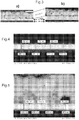
- the invention also relates to a semiconductor device 20 ( figure 2 ) using the conductive substrate 1 described above to form one or several photoactive layers 22, 24.
- the first photoactive layer 22 is typically a p-type doped layer, for example based on Cu copper chalcopyrite, indium In, and selenium Se and / or sulfur S. It may be, for example, as explained previously, from CIS, CIGS or CZTS.
- the second photoactive layer 24 is n-type doped and called buffer. It is for example composed of CdS (cadmium sulphide) and formed directly on the first photoactive layer 22.
- the buffer layer 24 is for example based on In x S y , Zn (O, S), or ZnMgO or in another material of any suitable type.
- the cell does not comprise a buffer layer, the first photoactive layer 22 itself being able to form a pn homojunction.
- the first photoactive layer 22 is a p-type or homojunction p-n layer obtained by addition of alkaline elements.
- the deposition of the photoactive layer comprises selenization and / or sulfurization steps, as explained in more detail below.
- the deposition can be carried out by evaporation of the elements Cu, In, Ga and Se (or Cu, Sn, Zn, S).
- the top layer 12 based on the metal M is converted into a layer 12 'based on M (S, Se) 2 . This transformation concerns for example the entirety of the upper layer 12.
- the invention also relates to a photovoltaic cell 30 comprising a semiconductor device 20 as described above.
- the transparent electrode coating 32 alternatively comprises a layer of zinc oxide doped with gallium, or boron, or a layer of ITO.
- TCO transparent conductive material
- a metal grid (not shown on the figure 2 ) is then optionally deposited on the transparent electrode coating 32, for example through a mask, for example by electron beam. It is for example a grid of Al (aluminum) for example of approximately 2 .mu.m thick on which is deposited a grid of Ni (nickel) for example about 50nm thick to protect the layer of Al .
- the cell 30 is then protected from external aggression. It comprises for example for this purpose a counter-substrate (not shown) covering the front electrode coating 32 and laminated to the carrier substrate 2 via a lamination interlayer (not shown) made of thermoplastic material. This is for example a sheet of EVA, PU or PVB.
- the invention also relates to a photovoltaic module comprising a plurality of photovoltaic cells formed on the same substrate 2, connected in series with each other and obtained by the margins of the layers of the semiconductor device 20.
- the invention further relates to a method of manufacturing the semiconductor device 20 and the photovoltaic cell 30 above, which method comprises a step of forming a photoactive layer by selenization and / or sulfurization.
- the photoactive layer 22 is for example a layer of CIGS formed as follows.
- the precursors of the layer are deposited on the electrode coating 6.
- a metal stack consisting of an alternation of CuGa and In type layers is for example deposited by magnetron cathode sputtering at ambient temperature, on the electrode coating 6.
- a selenium layer is then deposited at ambient temperature directly on the metal stack, for example by thermal evaporation.
- the metal stack has, for example, a multilayer structure of Cu / In / Ga / Cu / In / Ga type.
- the substrate undergoes a high temperature heating treatment called RTP ("Rapid Thermal Process, RTP" in English), for example at about 520 ° C in an atmosphere composed for example of sulfur gas, for example based on of S or H 2 S, thus forming a layer of CuIn x Ga 1-x (S, Se) 2 .
- RTP Rapid Thermal Process, RTP
- An advantage of this process is that it does not require an external source of selenium vapor.
- the loss of some of the selenium during heating is compensated by a deposit of excess selenium on the metal stack.
- the selenium required for selenization is provided by the deposited selenium layer.
- the selenization is obtained without the deposition of a selenium layer but by an atmosphere containing selenium gas, for example based on Se or H 2 Se, prior to exposure to a sulfur-rich atmosphere.
- the sulphurization step may optionally abstain from a buffer layer, for example CdS.
- an alkali-based layer for example sodium
- a precise determination of sodium in the photoactive layer it may be advantageous to deposit an alkali-based layer, for example sodium, for a precise determination of sodium in the photoactive layer.
- the alkalis Prior to the deposition of the CuGa and In metal stack, the alkalis are introduced, for example, by depositing, on the sacrificial layer 12 based on molybdenum, a layer of sodium selenide or a compound containing sodium so as to introduce for example of the order of 2.10 15 sodium atoms per cm 2 .
- the metal stack is deposited directly on this layer of sodium selenide.
- CI (G) S or CZTS there are numerous possible variants for forming the layers of CI (G) S or CZTS, which include, for example, coevaporation of the elements mentioned above, chemical vapor deposition, electrochemical deposition of metals, selenides or chalcopyrites. , the reactive sputtering of metals or selenides in the presence of H 2 Se or H 2 S.
- the method of manufacturing the photoactive layer 22 is of any suitable type.
- All methods of manufacturing CIS or CZTS type layers use a high temperature heating step in the presence of selenium and / or sulfur in the vapor state or in the liquid state.
- a carrier substrate 2 made of soda-lime-silica glass with a thickness of 3 mm was used, with an alkaline barrier layer consisting of Si 3 N 4 and having a thickness of 140 nm deposited directly on the substrate. 2 glass carrier.
- the photovoltaic cells were produced by Cu (In, Ga) (S, Se) 2 formation in two steps.
- a precursor stack containing Cu, Ga, In and Na was deposited by magnetron sputtering as described above.
- a layer of selenium was then deposited by thermal evaporation.
- the precursor stack was then converted to Cu (In, Ga) (S, Se) 2 by a rapid RTP heating process in a sulfur-containing atmosphere.
- a layer 24 of CdS was then deposited, followed by a layer 32 of ZnO: Al.
- Photovoltaic cells with an opening area of 1.4 cm 2 were produced by depositing a grid on the ZnO: Al layer.
- Modules of 30x30cm were manufactured by monolithic interconnection.
- Figures 3a and 3nb illustrate the effect of the barrier layer on selenization.
- Figure 3b Due to a high temperature and a high selenium partial pressure, the thickness of the Mo (S, Se) 2 compound formed is several hundred nanometers, leaving only a very thin thickness of metallic Mo.
- Figure 3a the selenization barrier layer prevents the selenization of the molybdenum layer that it protects.
- figure 4 is an electron microscopy image showing a 3mm glass substrate, a silicon nitride-based alkaline barrier layer, 130nm, a 30nm titanium nitride layer and a 25nm molybdenum layer, before treatment.
- the figure 5 shows in turn the same substrate as on the figure 4 after deposition of the photoactive layer and selenization.
- the total thickness of the back electrode, including the Mo (S, Se) 2 layer and the selenization barrier layer varies between 460nm and 480 nm, the thickness of the layer of Mo (S, Se) 2 varying between 70nm and 80nm.
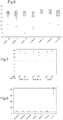
- the Figures 6 and 7 illustrate the energy conversion coefficient obtained as a function of the different conductive substrates used.
- the figure 6 presents results of experiment obtained for photovoltaic cells differing from each other by the thickness of the selenization barrier layer, in TiON or MoON (Examples 1 to 6), and comparing these results to a photovoltaic cell with conductive substrate without layer barrier to selenization and thick molybdenum layer (Example 7).
- the efficiency of the cell is in ordinates in%.
- Examples 1 to 6 show an advantage in using a TiON barrier layer rather than a MoON barrier layer.
- the optimum thickness is about 15 nm.
- Example 7 Comparing the results of Examples 1 to 6 with Example 7 further shows that it is possible to obtain equivalent performances with electrode coatings combining only 230 nm of Mo, ie 195 nm less than in Example 7, a substantial saving of material.
- a selenization barrier layer even of 5 nm, whether the material is TiON or MoON, has a protective effect against the selenization of the molybdenum-based main layer 8.
- the molybdenum-based upper layer 12 has been completely transformed into MoSe 2 .
Landscapes
- Photovoltaic Devices (AREA)
- Life Sciences & Earth Sciences (AREA)
- Engineering & Computer Science (AREA)
- Sustainable Development (AREA)
- Sustainable Energy (AREA)
- Electrodes Of Semiconductors (AREA)
Description
L'invention se rapporte au domaine des cellules photovoltaïques, plus particulièrement au domaine des substrats conducteurs à base de molybdène utilisés pour fabriquer des cellules photovoltaïques à couches minces.The invention relates to the field of photovoltaic cells, more particularly to the field of molybdenum-based conductive substrates used to produce thin-film photovoltaic cells.
En effet, de façon connue, certaines cellules photovoltaïques à couches minces, dites de seconde génération, utilisent un substrat conducteur à base de molybdène revêtu d'une couche d'agent absorbeur (i.e. matériau photoactif), généralement en chalcopyrite de cuivre Cu, d'indium In, et de sélénium Se et/ou de soufre S. II peut s'agir, par exemple, d'un matériau du type CuInSe2. Ce type de matériau est connu sous l'abréviation CIS. II peut également s'agir de CIGS c'est-à-dire d'un matériau incorporant en outre du gallium, ou encore de matériaux du type Cu2(Zn,Sn)(S,Se)4 (i.e. CZTS), utilisant du zinc et/ou de l'étain plutôt que de l'indium et/ou du gallium.Indeed, in known manner, certain thin-film photovoltaic cells, called second-generation, use a conductive substrate based on molybdenum coated with a layer of absorber (ie photoactive material), generally copper chalcopyrite Cu, d indium In, and Se selenium and / or sulfur S. It may be, for example, a CuInSe 2 type material. This type of material is known under the abbreviation CIS. It may also be CIGS, that is to say a material that additionally incorporates gallium, or materials of the Cu 2 (Zn, Sn) (S, Se) 4 (ie CZTS) type, using zinc and / or tin rather than indium and / or gallium.
Pour ce type d'application, les électrodes sont le plus souvent à base de molybdène (Mo) car ce matériau présente un certain nombre d'avantages. C'est un bon conducteur électrique (résistivité relativement faible de l'ordre de 10µΩ.cm). II peut être soumis aux traitements thermiques élevés nécessaires, car il a un point de fusion élevé (2610°C). II résiste, dans une certaine mesure, au sélénium et au soufre. Le dépôt de la couche d'agent absorbeur impose le plus souvent un contact avec une atmosphère contenant du sélénium ou du soufre qui tend à détériorer la plupart des métaux. Le molybdène réagit avec le sélénium ou le soufre notamment, formant du MoSe2, MoS2 ou Mo(S,Se)2, mais garde l'essentiel de ses propriétés, notamment électriques, et conserve un contact électrique adéquat avec par exemple la couche de CIS, de CIGS, ou de CZTS. Enfin, c'est un matériau sur lequel les couches de type CIS, CIGS ou CZTS adhèrent bien, le molybdène tend même à en favoriser la croissance cristalline.For this type of application, the electrodes are most often based on molybdenum (Mo) because this material has a number of advantages. It is a good electrical conductor (relatively low resistivity of the order of 10μΩ.cm). It can be subjected to the necessary high heat treatments because it has a high melting point (2610 ° C). It resists, to a certain extent, selenium and sulfur. Deposition of the absorber layer most often requires contact with an atmosphere containing selenium or sulfur which tends to deteriorate most metals. Molybdenum reacts with selenium or sulfur in particular, forming MoSe 2 , MoS 2 or Mo (S, Se) 2 , but retains most of its properties, especially electrical properties, and maintains adequate electrical contact with, for example, the layer CIS, CIGS, or CZTS. Finally, it is a material on which the layers of CIS, CIGS or CZTS type adhere well, molybdenum even tends to promote crystal growth.
Cependant, le molybdène présente un inconvénient important quand on envisage une production industrielle : c'est un matériau coûteux. En effet, les couches en molybdène sont habituellement déposées par pulvérisation cathodique (assistée par champ magnétique). Or les cibles de molybdène sont onéreuses. Cela est d'autant moins négligeable que pour obtenir le niveau de conductivité électrique voulu (une résistance par carré inférieure ou égale à 20/□, et de préférence inférieure ou égale à 1 ou même 0,5Ω/□ après traitement dans une atmosphère contenant du S ou du Se), il faut une couche de Mo relativement épaisse, généralement de l'ordre de 400 nm à 1 micromètre.However, molybdenum has a significant disadvantage when considering industrial production: it is an expensive material. Indeed, the molybdenum layers are usually deposited by sputtering (magnetic field assisted). But molybdenum targets are expensive. This is all the less negligible as to obtain the level of desired electrical conductivity (a resistance per square less than or equal to 20 / □, and preferably less than or equal to 1 or even 0.5Ω / □ after treatment in an atmosphere containing S or Se), a layer of Mo is required relatively thick, generally of the order of 400 nm to 1 micrometer.
La demande de brevet
Ce type de substrat conducteur reste néanmoins relativement coûteux.This type of conductive substrate is nevertheless relatively expensive.
Un but de la présente invention est de fournir un nouveau substrat conducteur à base de molybdène dont le coût de fabrication soit relativement faible.An object of the present invention is to provide a new conductive substrate based on molybdenum whose manufacturing cost is relatively low.
A cet effet, la présente invention a notamment pour objet un substrat conducteur pour cellule photovoltaïque, comprenant un substrat porteur et un revêtement électrode formé sur le substrat porteur, dans lequel le revêtement électrode comprend :
- une couche principale à base de molybdène formée sur le substrat porteur ;
- une couche barrière à la sélénisation formée sur la couche principale à base de molybdène, la couche barrière à la sélénisation ayant une épaisseur inférieure à 50nm, de préférence inférieure ou égale à 30nm, de préférence encore inférieure ou égale à 20nm ; et
- sur la couche barrière à la sélénisation, une couche supérieure à base d'un métal M propre à former, après sulfuration et/ou sélénisation, une couche de contact ohmique avec un matériau semi-conducteur photoactif.
- a molybdenum-based main layer formed on the carrier substrate;
- a selenization barrier layer formed on the molybdenum-based main layer, the selenization barrier layer having a thickness of less than 50 nm, preferably less than or equal to 30 nm, more preferably less than or equal to 20 nm; and
- on the selenization barrier layer, an upper layer based on a metal M capable of forming, after sulfurization and / or selenization, an ohmic contact layer with a photoactive semiconductor material.
Un tel substrat conducteur présente l'avantage de permettre d'obtenir, avec des épaisseurs moindres de molybdène, une résistance par carré équivalente à celle d'un substrat conducteur dont le revêtement électrode est constitué d'une seule couche de molybdène.Such a conductive substrate has the advantage of making it possible to obtain, with smaller thicknesses of molybdenum, a square resistance equivalent to that of a conductive substrate whose electrode coating consists of a single layer of molybdenum.
Grâce au substrat conducteur, le procédé de fabrication de la cellule photovoltaïque (ou module photovoltaïque) est en outre particulièrement fiable. La couche barrière à la sélénisation permet en effet à la fois de garantir la présence et la quantité de Mo(S,Se)2 par la transformation de l'intégralité de la couche supérieure (par exemple si son épaisseur est entre 10 et 50nm) tout en garantissant la présence et une épaisseur uniforme d'une couche principale à base de molybdène dont les propriétés de conductance ont été préservées. La préservation des qualités de la couche principale à base de molybdène et l'uniformité de son épaisseur permettent de réduire les quantités de matériaux au plus juste.Thanks to the conductive substrate, the manufacturing process of the photovoltaic cell (or photovoltaic module) is also particularly reliable. The barrier layer to selenization makes it possible at the same time to guarantee the presence and the amount of Mo (S, Se) 2 by the transformation of the entire upper layer (for example if its thickness is between 10 and 50nm) while guaranteeing the presence and uniform thickness of a main layer to molybdenum base whose conductance properties have been preserved. Preserving the qualities of the molybdenum-based main layer and the uniformity of its thickness make it possible to reduce the quantities of materials to a minimum.
L'uniformité de la couche de contact ohmique formée par la couche supérieure après sélénisation et/ou sulfuration bénéficie en outre à l'efficacité de la cellule solaire.The uniformity of the ohmic contact layer formed by the upper layer after selenization and / or sulphurization further benefits the efficiency of the solar cell.
- la couche barrière à la sélénisation est à base d'un nitrure ou d'un oxynitrure métallique avec le métal M choisi parmi le titane, le molybdène, le zirconium ou le tantale et une teneur en oxygène x=O/(O+N) avec x= 0 ou 0<x<1 ;
- la couche barrière à la sélénisation est à base d'un oxynitrure métallique avec le métal M choisi parmi le titane, le molybdène, le zirconium ou le tantale et une teneur en oxygène x=O/(O+N) avec 0<x<1, par
exemple exemple 0,1<x<0,9 ; - la couche barrière à la sélénisation a une résistivité comprise entre 200µOhm.cm et 500µOhm.cm ;
- la couche barrière à la sélénisation est un composé à base de molybdène avec une teneur élevée en oxygène et/ou en azote ;
- la couche barrière à la sélénisation a une résistivité comprise entre 20µOhm.cm et 50µOhm.cm ;
- ledit métal M est propre à former un composé de type sulfure et/ou séléniure semi-conducteur de type p avec une concentration de porteurs de charge supérieure ou égale à 1016/cm3 et un travail de sortie supérieur ou égal à 4,5eV ;
- ladite couche supérieure à base d'un métal M est à base de molybdène et/ou de tungstène ;
- ladite couche supérieure à base d'un métal M a une épaisseur supérieure ou égale à 10nm, de préférence supérieure ou égale à 20nm et inférieure ou inférieure ou égale à 100nm, de préférence inférieure ou égale à 50nm ;
- la couche barrière à la sélénisation a une épaisseur supérieure ou égale à 3nm, de préférence supérieure ou égale à 5nm ;
- la couche principale à base de molybdène a une épaisseur inférieure ou égale à 400nm, par exemple inférieure ou égale à 300nm, par exemple inférieure ou égale à 250nm ;
- la couche principale à base de molybdène a une épaisseur supérieure ou égale à 40nm, de préférence supérieure ou égale à 150nm ;
- la couche principale à base de molybdène a une épaisseur uniforme, l'épaisseur restant de préférence dans un intervalle de +/-10% par rapport à une valeur moyenne ;
- le revêtement électrode a une résistance par carré inférieure ou égale à 2Ω/□, de préférence inférieure ou égale à 1Ω/□ ;
- ladite couche supérieure à base d'un métal M est formée directement sur la couche barrière à la sélénisation ;
- la couche barrière à la sélénisation est formée directement sur.la couche principale à base de molybdène ;
- le substrat porteur est dans un matériau contenant des alcalins, le substrat conducteur comprenant une ou plus couches barrières aux alcalins formées sur le substrat porteur et sous la couche principale à base de molybdène, la ou les couches barrières aux alcalins étant par exemple à base de l'un des matériaux choisis parmi : le nitrure, l'oxyde, l'oxynitrure ou l'oxycarbure de silicium, l'oxyde ou l'oxynitrure d'aluminium ;
- le substrat porteur est une feuille de verre.
- the barrier layer for selenization is based on a metal nitride or oxynitride with the metal M chosen from titanium, molybdenum, zirconium or tantalum and an oxygen content x = O / (O + N) with x = 0 or 0 <x <1;
- the barrier layer for selenization is based on a metal oxynitride with the metal M selected from titanium, molybdenum, zirconium or tantalum and an oxygen content x = O / (O + N) with 0 <x < 1, for example 0.05 <x <0.95, for example 0.1 <x <0.9;
- the barrier layer for selenization has a resistivity of between 200 .mu.m.cm and 500 .mu.m.cm;
- the selenization barrier layer is a molybdenum compound with a high content of oxygen and / or nitrogen;
- the barrier layer for selenization has a resistivity of between 20 .mu.m.cm and 50 .mu.m.cm;
- said metal M is capable of forming a sulphide-type compound and / or p-type semiconductor selenide with a charge carrier concentration greater than or equal to 10 16 / cm 3 and an output work greater than or equal to 4.5eV;
- said upper layer based on a metal M is based on molybdenum and / or tungsten;
- said upper layer based on a metal M has a thickness greater than or equal to 10 nm, preferably greater than or equal to 20 nm and less than or equal to 100 nm, preferably less than or equal to 50 nm;
- the barrier layer for selenization has a thickness greater than or equal to 3 nm, preferably greater than or equal to 5 nm;
- the molybdenum-based main layer has a thickness less than or equal to 400 nm, for example less than or equal to 300 nm, for example less than or equal to 250 nm;
- the main layer based on molybdenum has a thickness greater than or equal to 40 nm, preferably greater than or equal to 150 nm;
- the molybdenum-based main layer has a uniform thickness, the thickness preferably remaining within +/- 10% of a mean value;
- the electrode coating has a square resistance of less than or equal to 2Ω / □, preferably less than or equal to 1Ω / □;
- said metal-based top layer is formed directly on the selenization barrier layer;
- the selenization barrier layer is formed directly on the molybdenum-based main layer;
- the carrier substrate is in a material containing alkalis, the conductive substrate comprising one or more alkali barrier layers formed on the carrier substrate and under the molybdenum-based main layer, the alkali barrier layer or layers being for example based on one of the materials chosen from: silicon nitride, oxide, oxynitride or oxycarbide, aluminum oxide or oxynitride;
- the carrier substrate is a glass sheet.
L'invention a également pour objet un dispositif semi-conducteur comprenant un substrat porteur et un revêtement électrode formé sur le substrat porteur, le revêtement électrode comprenant :
- une couche principale à base de molybdène ;
- une couche barrière à la sélénisation formée sur la couche principale à base de molybdène, la couche barrière à la sélénisation ayant une épaisseure inférieure à 50 nm;
- une couche photoactive en un matériau semi-conducteur photoactif à base de chalcopyrite de cuivre et de sélénium et/ou de soufre, par exemple un matériau de type Cu(In,Ga)(S,Se)2, notamment CIS ou CIGS, ou encore un matériau de type Cu2(Zn,Sn)(S,Se)4, la couche photoactive étant formée sur la couche barrière à la sélénisation ; et
- entre la couche barrière à la sélénisation et la couche photoactive, une couche de contact ohmique à base d'un composé de type sulfure et/ou séléniure d'un métal M.
- a main layer of molybdenum;
- a selenization barrier layer formed on the molybdenum-based main layer, the selenization barrier layer having a thickness of less than 50 nm;
- a photoactive layer made of a photoactive semiconducting material based on copper chalcopyrite and selenium and / or sulfur, for example a Cu (In, Ga) type material (S, Se) 2 , in particular CIS or CIGS, or still a Cu 2 (Zn, Sn) material (S, Se) 4 , the photoactive layer being formed on the selenization barrier layer; and
- between the selenization barrier layer and the photoactive layer, an ohmic contact layer based on a sulfide compound and / or selenide of a metal M.
Suivant des modes particuliers de réalisation, le dispositif semi-conducteur comporte l'une ou plusieurs des caractéristiques suivantes, prise(s) isolément ou suivant toutes les combinaisons techniquement possibles :
- le matériau de la couche de contact ohmique est un matériau semi-conducteur de type p avec une concentration de porteurs de charge supérieure ou égale à 1016/cm3 et un travail de sortie supérieur ou égal à 4,5eV ;
- la couche de contact ohmique est à base d'un composé de type sulfure et/ou séléniure de molybdène et/ou de tungstène.
- the ohmic contact layer material is a p-type semiconductor material with a charge carrier concentration greater than or equal to 10 16 / cm 3 and an output work greater than or equal to 4.5 eV;
- the ohmic contact layer is based on a compound of the sulfide and / or selenide type of molybdenum and / or tungsten.
L'invention a encore pour objet une cellule photovoltaïque comprenant un dispositif semi-conducteur tel que décrit ci-dessus, et un revêtement électrode transparent formé sur la couche photoactive.The invention further relates to a photovoltaic cell comprising a semiconductor device as described above, and a transparent electrode coating formed on the photoactive layer.
Un autre objet de l'invention est un module photovoltaïque comprenant une pluralité de cellules photovoltaïques reliées entre elles en série et toutes formées sur le même substrat, dans lequel les cellules photovoltaïques sont telles que décrites ci-dessus.Another object of the invention is a photovoltaic module comprising a plurality of photovoltaic cells interconnected in series and all formed on the same substrate, in which the photovoltaic cells are as described above.
L'invention a également pour objet un procédé de fabrication d'un substrat conducteur pour cellule photovoltaïque, comprenant des étapes consistant à :
- déposer une couche principale à base de molybdène sur un substrat porteur;
- déposer une couche barrière à la sélénisation sur la couche principale à base de molybdène, la couche barrière à la sélénisation ayant une épaisseur inférieure à 50 nm;
- déposer, sur la couche barrière à la sélénisation, une couche supérieure à base d'un métal M propre à former, après sulfuration et/ou sélénisation, une couche de contact ohmique avec un matériau semi-conducteur photoactif ; et
- transformer la couche supérieure à base de métal M en un sulfure et/ou séléniure du métal M.
- depositing a molybdenum-based main layer on a carrier substrate;
- depositing a selenization barrier layer on the molybdenum-based main layer, the selenization barrier layer having a thickness of less than 50 nm;
- depositing, on the selenization barrier layer, an upper layer based on a metal M capable of forming, after sulfurization and / or selenization, an ohmic contact layer with a photoactive semiconductor material; and
- transforming the upper layer based on metal M into a sulfide and / or metal selenide M.
Suivant des modes particuliers de réalisation, le procédé présente l'une ou plusieurs des caractéristiques suivantes, prise(s) isolément ou suivant toutes les combinaisons techniquement possibles :
- le procédé comprend une étape de formation d'une couche photoactive par sélénisation et/ou sulfuration, sur ladite couche supérieure à base d'un métal M, l'étape de transformation de ladite couche supérieure à base d'un métal M étant réalisée avant ou pendant la formation de ladite couche photoactive, de préférence pendant ;
- après sulfuration et/ou sélénisation, ladite couche supérieure est à base d'un semi-conducteur de type p avec une concentration de porteurs de charge supérieure ou égale à 1016/cm3 et un travail de sortie supérieur ou égal à 4,5eV ;
- après sulfuration et/ou sélénisation, ladite couche supérieure est un composé à base de sulfure et/ou séléniure de molybdène et/ou de tungstène ;
- l'étape de formation de la couche photoactive comprenant une étape de sélénisation et/ou sulfuration à une température supérieure ou égale à 300°C.
- the method comprises a step of forming a photoactive layer by selenization and / or sulphidation, on said upper layer based on a metal M, the step of transforming said upper layer based on a metal M being carried out before or during the formation of said photoactive layer, preferably during;
- after sulphurization and / or selenization, said upper layer is based on a p-type semiconductor with a charge carrier concentration greater than or equal to 10 16 / cm 3 and an output work greater than or equal to 4.5eV ;
- after sulphurisation and / or selenization, said upper layer is a compound based on sulphide and / or selenide of molybdenum and / or tungsten;
- the step of forming the photoactive layer comprising a selenization and / or sulphurization step at a temperature greater than or equal to 300 ° C.
L'invention sera mieux comprise à la lecture de la description qui va suivre, donnée uniquement à titre d'exemple, et faite en référence aux dessins annexés, sur lesquels :
- la
figure 1 est une vue schématique en coupe d'un substrat conducteur ; - la
figure 2 est une vue schématique en coupe d'une cellule photovoltaïque comprenant un substrat conducteur selon lafigure 1 ; - les
figures 3a et 3b sont des vues en coupe obtenues par microscopie électronique, lafigure 3b représentant un dispositif semi-conducteur après traitement à haute température et haute pression partielle en sélénium et dont le substrat conducteur ne possédait à l'origine qu'une seule couche de molybdène tandis qu'il possédait en outre sur lafigure 3a une couche barrière à la sélénisation, à base de TiON, et une couche supérieure de contact ohmique, à base de Mo ;
- la
figure 4 est une image en coupe par microscopie électronique de la section d'un substrat conducteur amélioré; - la
figure 5 est une image analogue à celle de lafigure 4 d'un dispositif semi-conducteur dans lequel une couche mince CIGSSe a été formée par sélénisation sur le substrat conducteur de lafigure 4 ; - les
figures 6 et 7 illustrent l'efficacité de cellules utilisant des substrats conducteurs Si3N4 (140nm) / Mo avec différentes épaisseurs de Mo avec et sans couche barrière à la sélénisation ; et - la
figure 8 montre des résultats expérimentaux de tests de sélénisation tel que décrits ci-dessous.
- the
figure 1 is a schematic sectional view of a conductive substrate; - the
figure 2 is a schematic sectional view of a photovoltaic cell comprising a conductive substrate according to thefigure 1 ; - the
Figures 3a and 3b are sectional views obtained by electron microscopy, thefigure 3b representing a semiconductor device after treatment at high temperature and high partial pressure selenium and whose conductive substrate originally had only one layer of molybdenum while it also possessed on thefigure 3a a barrier layer to selenization, based on TiON, and an upper layer of ohmic contact, based on Mo;
- the
figure 4 is an electron microscopic sectional view of the section of an improved conductive substrate; - the
figure 5 is an image similar to that of thefigure 4 of a semiconductor device in which a thin layer CIGSSe has been formed by selenization on the conductive substrate of thefigure 4 ; - the
Figures 6 and 7 illustrate the efficiency of cells using Si 3 N 4 (140 nm) / Mo conducting substrates with different thicknesses of Mo with and without selenization barrier layer; and - the
figure 8 shows experimental results of selenization tests as described below.
Les dessins des
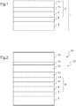
Sur la
- un substrat porteur 2 en verre ;
- une couche barrière aux alcalins 4 formée sur le substrat 2 ; et
un revêtement électrode 6 à base de molybdène formé sur la couche barrière aux alcalins 4.
- a
carrier substrate 2 made of glass; - an
alkali barrier layer 4 formed on thesubstrate 2; and - a molybdenum-based
electrode coating 6 formed on thealkali barrier layer 4.
On entend, dans tout le texte, par « une couche A formée (ou déposée) sur une couche B », une couche A formée soit directement sur la couche B et donc en contact avec la couche B, soit formée sur la couche B avec interposition d'une ou plusieurs couches entre la couche A et la couche B.Throughout the text is meant by "a layer A formed (or deposited) on a layer B", a layer A formed either directly on the layer B and therefore in contact with the layer B, or formed on the layer B with interposition of one or more layers between layer A and layer B.
A noter qu'on entend dans tout le texte par « revêtement électrode », un revêtement d'amenée de courant comprenant au moins une couche électroniquement conductrice, c'est-à-dire dont la conductivité est assurée par la mobilité des électrons.Note that throughout the text "electrode coating" means a current supply coating comprising at least one electronically conductive layer, that is to say the conductivity of which is ensured by the mobility of the electrons.
En outre, dans tout le texte, « comprend une couche » doit bien entendu s'entendre comme « comprend au moins une couche ».In addition, throughout the text, "includes a layer" must of course be understood as "includes at least one layer".
Le revêtement électrode 6 illustré est constitué :
- d'une couche principale 8 à base de molybdène formée directement sur la couche barrière aux alcalins 4 ;
- d'une couche barrière à la sélénisation 10 formée directement sur la couche principale 8 à base de molybdène et de faible épaisseur ; et
- d'une couche supérieure 12 à base d'un métal M, formée directement sur la couche barrière à la sélénisation 10.
- of a
main layer 8 based on molybdenum formed directly on thealkali barrier layer 4; - a
selenization barrier layer 10 formed directly on the molybdenum-basedmain layer 8 and of small thickness; and - an
upper layer 12 based on a metal M, formed directly on theselenization barrier layer 10.
Un tel substrat conducteur 1 est destiné à la fabrication d'un matériau photoactif avec adjonction de sodium (il est connu que le sodium améliore les performances des matériaux photoactifs de type CIS ou CIGS). La couche barrière aux alcalins 4 empêche la migration des ions sodium depuis le substrat 2 en verre, pour un meilleur contrôle de l'adjonction de sodium dans le matériau photoactif.Such a conductive substrate 1 is intended for the manufacture of a photoactive material with added sodium (it is known that sodium improves the performance of photoactive materials of CIS or CIGS type). The
Dans le cas où le substrat ne contient pas d'ions alcalins, la couche barrière aux alcalins 4 peut être omise.In the case where the substrate does not contain alkali ions, the
Une autre technique de fabrication du matériau photoactif consiste à utiliser la migration des ions sodium depuis le substrat porteur en verre pour former le matériau photoactif. Dans ce cas, le substrat conducteur 1 ne possède pas de couche barrière aux alcalins 4 et la couche principale 8 de molybdène est par exemple formée directement sur le substrat porteur 2.Another technique for making the photoactive material is to use the migration of sodium ions from the glass substrate to form the photoactive material. In this case, the conductive substrate 1 does not have an
En variante également, le revêtement électrode 6 comprend une ou plusieurs couches intercalaires.Alternatively also, the
Ainsi, d'une manière générale, le substrat conducteur 1 comprend un substrat porteur 2 et un revêtement électrode 6 comprenant :
- une couche principale 8 à base de molybdène formée sur le substrat porteur 2 ;
- une couche barrière à la sélénisation 10 formée sur la couche principale 8 à base de molybdène ; et
- une couche supérieure 12 à base d'un métal M formée sur la couche barrière à la sélénisation 10.
- a molybdenum-based
main layer 8 formed on thecarrier substrate 2; - a
selenization barrier layer 10 formed on the molybdenum-basedmain layer 8; and - an
upper layer 12 based on a metal M formed on theselenization barrier layer 10.
Le métal M est propre à former, après sulfuration et/ou sélénisation, une couche de contact ohmique avec un matériau semi-conducteur photoactif, notamment avec un matériau semi-conducteur photoactif à base de chalcopyrite de cuivre et de sélénium et/ou de soufre par exemple un matériau photoactif de type Cu(In,Ga)(S,Se)2, notamment CIS ou CIGS, ou encore un matériau de type Cu2(Zn,Sn)(S,Se)4.The metal M is capable of forming, after sulfurization and / or selenization, an ohmic contact layer with a photoactive semiconductor material, in particular with a photoactive semiconductor material based on copper chalcopyrite and selenium and / or sulfur for example a Cu (In, Ga) (S, Se) 2 type of photoactive material, in particular CIS or CIGS, or a Cu 2 (Zn, Sn) material (S, Se) 4 .
On entend par une couche de contact ohmique une couche d'un matériau tel que la caractéristique courant / tension du contact est non-rectifiante et linéaire.An ohmic contact layer is understood to mean a layer of a material such that the current / voltage characteristic of the contact is non-rectifying and linear.
De préférence, la couche supérieure 12 est la dernière couche supérieure du revêtement électrode 6, c'est-à-dire que le revêtement électrode 6 ne possède pas une autre couche au-dessus de la couche 12.Preferably, the
De préférence également, le revêtement électrode 6 comprend une seule couche principale 8 à base de molybdène, une seule couche barrière à la sélénisation 10, et une seule couche 12.Also preferably, the
II est à noter qu'on entend, dans tout le texte, par « une seule couche », une couche d'un même matériau. Cette unique couche peut néanmoins être obtenue par la superposition de plusieurs couches d'un même matériau, entre lesquelles existe une interface qu'il est possible de caractériser, comme décrit dans
Typiquement, dans une enceinte de dépôt magnétron, plusieurs couches d'un même matériau seront formées successivement sur le substrat porteur par plusieurs cibles pour former au final une seule couche du même matériau, à savoir le molybdène.Typically, in a magnetron deposition chamber, several layers of the same material will be successively formed on the carrier substrate by several targets to ultimately form a single layer of the same material, namely molybdenum.
A noter qu'on entend par le terme « à base de molybdène », un matériau composé d'une quantité substantielle de molybdène, c'est-à-dire soit un matériau constitué seulement de molybdène, soit un alliage comprenant majoritairement du molybdène, soit un composé comprenant majoritairement du molybdène mais avec une teneur en oxygène et/ou en azote, par exemple une teneur conduisant à une résistivité supérieure ou égale à 20µOhm.cm.It should be noted that the term "molybdenum-based" refers to a material composed of a substantial quantity of molybdenum, that is to say either a material consisting solely of molybdenum, or an alloy comprising mainly molybdenum, or a compound comprising predominantly molybdenum but with a content of oxygen and / or nitrogen, for example a content leading to a resistivity of greater than or equal to 20 .mu.m.
La couche 12 est destinée à être intégralement transformée par sélénisation et/ou sulfuration en Mo(S,Se)2, lequel matériau n'est en revanche pas considéré comme un matériau « à base de molybdène » mais un matériau à base de disulfure de molybdène, de diséléniure de molybdène ou d'un mélange de disulfure et de diséléniure de molybdène.The
De manière conventionnelle, la notation (S,Se) indique qu'il s'agit d'une combinaison de SxSe1-x avec 0≤x≤1.Conventionally, the notation (S, Se) indicates that it is a combination of S x Se 1-x with 0≤ x ≤1.
II est important de noter que le substrat illustré sur la
La couche supérieure 12, de façon à jouer son rôle de contact ohmique une fois transformée en Mo(S,Se)2, a par exemple une épaisseur supérieure ou égale à 10nm, et inférieure ou égale à 100nm, de préférence comprise entre 30nm et 50nm. Une épaisseur importante n'est pas nécessaire.The
Ledit métal M est avantageusement à base de molybdène et/ou de tungstène.Said metal M is advantageously based on molybdenum and / or tungsten.
Les composés de disulfure et/ou de diséléniure de molybdène Mo(S,Se)2 sont des matériaux dont l'efficacité comme couche de contact ohmique est prouvée. Le tungstène (W) est un matériau aux propriétés chimiques analogues. II forme également des semi-conducteurs chalcogénides WS2 et WSe2. Mo(S,Se)2 et W(S,Se)2 peuvent tous deux être formés comme des semi-conducteurs de type p avec un dopage de type p supérieur ou égal à 1016/cm3 et un travail de sortie d'environ 5ev. D'une manière générale, il peut s'agir d'un matériau à base d'un métal M propre à former un composé de type sulfure et/ou séléniure semi-conducteur de type p avec une concentration de porteurs de charge supérieure ou égale à 1016/cm3 et un travail de sortie supérieur ou égal à 4,5eV. Plus généralement encore, il s'agit d'un métal M de tout type apte à former, après sulfuration et/ou sélénisation, une couche de contact ohmique avec un matériau semi-conducteur photoactif, plus particulièrement avec un matériau photoactif à base de chalcopyrite de cuivre et de sélénium et/ou de soufre.Mo (S, Se) 2 molybdenum disulfide and / or diselenide compounds are materials whose effectiveness as an ohmic contact layer is proven. Tungsten (W) is a material with similar chemical properties. It also forms chalcogenide semiconductors WS 2 and WSe 2 . Mo (S, Se) 2 and W (S, Se) 2 can both be formed as p-type semiconductors with p-type doping greater than or equal to 10 16 / cm 3 and an output work of about 5ev. In general, it may be a material based on a metal M capable of forming a p-type compound of the sulphide type and / or semiconductor selenide with a concentration of charge carriers greater than or equal to at 10 16 / cm 3 and an output work greater than or equal to 4.5eV. More generally still, it is a metal M of any type capable of forming, after sulfurization and / or selenization, an ohmic contact layer with a photoactive semiconductor material, more particularly with a photoactive material based on chalcopyrite. copper and selenium and / or sulfur.
La couche barrière à la sélénisation 10 protège la couche principale 8 à base de molybdène d'une sélénisation et/ou sulfuration éventuelle. A noter qu'une couche protégeant de la sélénisation protège également de la sulfuration.The
On entend par couche barrière à la sélénisation, une couche d'un matériau de tout type adapté pour empêcher ou réduire la sélénisation des couches couvertes par la couche barrière à la sélénisation lors du dépôt, sur la couche barrière à la sélénisation, de couches de matériaux semi-conducteurs formés par sélénisation et/ou sulfuration. La couche barrière à la sélénisation au sens de l'invention montre une efficacité prouvée même à une épaisseur de 3nm.By selenization barrier layer is meant a layer of a material of any type adapted to prevent or reduce the selenization of the layers covered by the barrier layer to selenization during the deposition, on the selenization barrier layer, of layers of semiconductor materials formed by selenization and / or sulfurization. The barrier layer to selenisation in the sense of the invention shows a proven effectiveness even at a thickness of 3nm.
Un test possible pour savoir si un matériau est adapté ou non pour un rôle de barrière à la sélénisation est de comparer un échantillon avec et sans une couche de 5nm de ce matériau entre la couche supérieure 12 à base d'un métal M et la couche principale 8 et de faire subir une sélénisation aux échantillons, par exemple par chauffage à 520°C dans une atmosphère à 100% de sélénium. Si la sélénisation de la couche principale 8 est réduite ou empêchée et la couche supérieure 12 entièrement sélénisée, le matériau est efficace.A possible test as to whether a material is suitable or not for a role of barrier to selenization is to compare a sample with and without a layer of 5 nm of this material between the
Le matériau de la couche barrière à la sélénisation 10 est par exemple à base d'un nitrure de métal tel que le nitrure de titane, le nitrure de molybdène, le nitrure de zirconium ou le nitrure de tantale, ou une combinaison de ces matériaux. II peut également s'agir d'un oxynitrure.The material of the
D'une manière générale, il s'agit d'un matériau de tout type adapté pour protéger la couche principale 8 à base de molybdène d'une sélénisation ou sulfuration éventuelle.In general, it is a material of any type adapted to protect the
II peut également être à base d'un oxyde métallique tel que l'oxyde de molybdène, l'oxyde de titane ou un oxyde mixte de molybdène et de titane.It may also be based on a metal oxide such as molybdenum oxide, titanium oxide or a mixed oxide of molybdenum and titanium.
Les nitrures sont cependant préférés aux oxydes.Nitrides are however preferred to oxides.
De façon préférée encore, il s'agit d'un matériau à base d'un oxynitrure métallique avec M choisi parmi le titane, le molybdène, le zirconium ou le tantale, et avec un teneur en oxygène x= O/(O+N) avec 0<x<1, par exemple 0,05<x<0,95, par exemple 0,1<x<0,9.More preferably, it is a material based on a metal oxynitride with M selected from titanium, molybdenum, zirconium or tantalum, and with an oxygen content x = O / (O + N ) with 0 <x <1, for example 0.05 <x <0.95, for example 0.1 <x <0.9.
II est à noter que les nitrures, oxydes et oxynitrures ci-dessus peuvent être sous-stoechiométriques, stoechiométriques ou sur-stoechiométriques respectivement en azote et en oxygène.It should be noted that the above nitrides, oxides and oxynitrides may be substoichiometric, stoichiometric or superstoichiometric, respectively in nitrogen and in oxygen.
En variante, il s'agit d'une couche à base de molybdène, plus précisément d'un composé à base de molybdène avec une teneur élevée en oxygène et/ou en azote. La teneur en oxygène et/ou en azote est par exemple suffisante si elle induit une résistivité supérieure ou égale à 20µOhm.cm.Alternatively, it is a molybdenum-based layer, more specifically a molybdenum compound with a high content of oxygen and / or nitrogen. The oxygen content and / or nitrogen is for example sufficient if it induces a resistivity greater than or equal to 20 .mu.m.cm.
D'une manière générale, il s'agit donc d'une couche à base de molybdène avec une teneur élevée en oxygène et/ou en azote ou d'un matériau à base d'un nitrure, d'un oxyde ou d'un oxynitrure métallique adapté pour protéger la couche principale 8 à base de molybdène d'une sélénisation ou sulfuration éventuelle.In general, it is therefore a layer based on molybdenum with a high content of oxygen and / or nitrogen or a material based on a nitride, an oxide or a metal oxynitride suitable for protect the
La couche barrière à la sélénisation 10 est de faible épaisseur. Elle a une épaisseur inférieure à 50nm, de préférence inférieure ou égale à 30nm, de préférence encore inférieure ou égale à 15nm.The
Si la couche barrière à la sélénisation 10 est très fine, elle risque de ne plus avoir une influence significative. Elle a ainsi par exemple une épaisseur supérieure ou égale à 3nm, de préférence supérieure ou égale à 5nm. De façon surprenante, il s'est en effet avéré qu'une couche barrière à la sélénisation 10 d'une si faible épaisseur avait un effet significatif.If the
La couche barrière à la sélénisation 10 a une conductivité moindre que la couche principale 8 à base de molybdène. Elle a par exemple une résistivité comprise entre 200µOhm.cm et 500µOhm.cm dans le cas d'une couche à base d'une oxyde, nitrure ou oxynitrure métallique et une résistivité comprise entre 20µOhm.cm et 50µOhm.cm dans le cas d'un matériau à base de molybdène avec une teneur élevée en azote et/ou en oxygène.The
Du fait de la faible épaisseur de la couche barrière à la sélénisation 10, une résistivité élevée ne nuit pas aux performances de la cellule, le courant électrique passant transversalement.Due to the small thickness of the
La couche barrière à la sélénisation 10 est en outre de préférence apte à limiter la diffusion arrière des ions sodium vers le substrat porteur 2, c'est-à-dire la diffusion des ions sodium depuis le dessus de la couche supérieure 12, à travers la couche supérieure 12 et vers le substrat porteur 2.The
Cette propriété est avantageuse à plusieurs égards.This property is advantageous in many ways.
Elle fiabilise les procédé de fabrication consistant à ajouter des alcalins pour former le matériau photoactif, par exemple par dépôt de diséléniure de sodium sur la couche supérieure 12 du revêtement électrode 6 ou par adjonction de sodium pendant le dépôt du matériau photoactif, par exemple en utilisant des cibles contenant du sodium ou autres alcalins, comme décrit dans
La couche principale à base de molybdène 8 a une épaisseur suffisante pour que le revêtement électrode 6 ait, après un test de sélénisation tel que décrit ci-dessus, une résistance par carré inférieure ou égale à 2Ω/□, de préférence inférieure ou égale à 1Ω/□. La présence de la couche supérieure 12 à base du métal M et de la couche barrière à la sélénisation 10 permet d'atteindre de telles performances.The molybdenum-based
Dans l'hypothèse d'un revêtement électrode 6 ne comprenant pas d'autres couches électroconductrices que la couche principale 8 à base de molybdène, la couche barrière à la sélénisation 10 et la couche supérieure 12 à base du métal M, la couche principale à base de molybdène 8, pour avoir un effet significatif, a de préférence une épaisseur supérieure ou égale à 40nm, de préférence supérieure ou égale à 150nm. Toutefois, la couche principale à base de molybdène 8 a par exemple une épaisseur inférieure ou égale à 400nm, par exemple inférieure ou égale à 300nm, par exemple inférieure ou égale à 250nm.In the case of an
Diminuer l'épaisseur de la couche principale à base de molybdène 8 présente un avantage: permettre de déposer cette couche relativement fine par pulvérisation cathodique avec des paramètres de dépôt conduisant à une couche fortement contrainte, sans les problèmes de délamination que l'on peut rencontrer avec des couches épaisses.Decreasing the thickness of the molybdenum-based
La couche principale à base de molybdène 8 est par exemple constituée de molybdène, c'est-à-dire qu'elle comprend seulement du molybdène.The molybdenum-based
Le substrat porteur 2 et la couche barrière aux alcalins 4 vont maintenant être décrits.The
Deux cas sont à distinguer. Le cas où une migration d'ions alcalins depuis le substrat est souhaitée pour doper la couche de matériau photoactif et le cas où cette migration n'est pas souhaitée.Two cases are to be distinguished. The case where a migration of alkaline ions from the substrate is desired to dope the layer of photoactive material and the case where this migration is not desired.
Les substrats pourvus d'une ou plusieurs couches barrières aux alcalins 4 sont utilisés dans le deuxième cas notamment pour permettre d'utiliser comme substrat une feuille de verre de type silico-sodo-calcique obtenue par flottage, verre d'un coût relativement faible et qui présente toutes les qualités que l'on connait à ce type de matériau, comme par exemple sa transparence, son imperméabilité à l'eau et sa dureté.Substrates provided with one or more
La teneur en ions alcalins du substrat 2 est dans ce cas un inconvénient que la couche barrière aux alcalins vient minimiser.The alkali ion content of the
La couche barrière aux alcalins 4 est par exemple à base de l'un des matériaux choisis parmi : le nitrure, l'oxyde, l'oxynitrure ou l'oxycarbure de silicium, l'oxyde ou l'oxynitrure d'aluminium.The
En variante, toujours dans le deuxième cas, le substrat porteur 2 est une feuille d'un matériau de tout type adapté, par exemple un verre à base de silice ne contenant pas d'alcalins, tels que les verres borosilicatés, ou en matière plastique, ou même en métal.Alternatively, still in the second case, the
Dans le premier cas, le substrat porteur 2 est de tout type adapté et contient des alcalins, par exemple des ions sodium et potassium. Le substrat est par exemple un verre silico-sodo-calcique. La couche barrière aux alcalins est absente.In the first case, the
Dans les deux cas, le substrat porteur 2 est destiné à servir de contact arrière dans le module photovoltaïque et ne nécessite pas d'être transparent.In both cases, the
La feuille constituant le substrat porteur 2 peut être plane ou bombée, et présenter tout type de dimensions, notamment au moins une dimension supérieure à 1 mètre.The sheet constituting the
L'invention a également pour objet un procédé de fabrication du substrat conducteur 1 décrit ci-dessus.The invention also relates to a method of manufacturing the conductive substrate 1 described above.
Le procédé comprend des étapes consistant à :
- déposer la couche principale 8 base de molybdène sur le substrat porteur 2 , avec dépôt éventuel préalable de la couche barrière aux alcalins 4;
- déposer la couche barrière à la sélénisation 10 sur la couche principale 8 à base de molybdène, par exemple directement dessus ;
- déposer la couche supérieure 12 à base du métal M sur la couche barrière à la sélénisation 10 ; et
- transformer ladite couche à base de métal M en un sulfure et/ou séléniure du métal M. Cette étape de transformation peut être une étape séparée avant la formation la couche semi-conductrice CIS, CGS ou CZTS ou une étape réalisée pendant la sélénisation et/ou sulfuration de la couche semi-conductrice CIS, CGS ou CZTS, que cette sélénisation et/ou sulfuration soit réalisée pendant le dépôt de ladite couche semi-conductrice ou après le dépôt de composants métalliques dits précurseurs de la couche semi-conductrice.
- depositing the
molybdenum base layer 8 on thecarrier substrate 2, with optional preliminary deposition of thealkali barrier layer 4; - depositing the
selenization barrier layer 10 on the molybdenum-basedmain layer 8, for example directly on it; - depositing the
top layer 12 based on the metal M on theselenization barrier layer 10; and - transforming said metal-based layer M into metal sulfide and / or selenide M. This transformation step may be a separate step prior to forming the CIS, CGS or CZTS semiconductor layer or a step performed during selenization and / or or sulphidation of the CIS, CGS or CZTS semiconductor layer, whether this selenization and / or sulphurization is carried out during the deposition of said semiconductor layer or after the deposition of metal components known as precursors of the semiconductor layer.
Le dépôt des différentes couches est par exemple réalisé par pulvérisation cathodique assistée par magnétron mais il s'agit en variante d'un autre procédé de tout type adapté.The deposition of the various layers is for example carried out by magnetron assisted sputtering, but it is alternatively another method of any suitable type.
L'invention a également pour objet un dispositif semi-conducteur 20 (
La première couche photoactive 22 est typiquement une couche dopée de type p, par exemple à base de chalcopyrite de cuivre Cu, d'indium In, et de sélénium Se et/ou de soufre S. II peut s'agir, par exemple, comme expliqué précédemment, de CIS, CIGS ou CZTS.The first
La deuxième couche photoactive 24 est dopée de type n et dite tampon. Elle est par exemple composée de CdS (sulfure de cadmium) et formée directement sur la première couche photoactive 22.The second
En variante, la couche tampon 24 est par exemple à base de InxSy, Zn(O,S), ou ZnMgO ou dans un autre matériau de tout type adapté. En variante également, la cellule ne comprend pas de couche tampon, la première couche photoactive 22 pouvant elle-même former une homojonction p-n.As a variant, the
D'une manière générale, la première couche photoactive 22 est une couche de type p ou à homojonction p-n obtenue par addition d'éléments alcalins.In general, the first
Le dépôt de la couche photoactive comprend des étapes de sélénisation et/ou de sulfuration, comme expliqué plus en détail ci-dessous. Le dépôt peut être réalisé par évaporation des éléments Cu, In, Ga et Se (ou Cu, Sn, Zn, S). Lors de ces étapes de sélénisation et/ou de sulfuration, la couche supérieure 12 à base du métal M est transformée en une couche 12' à base de M(S,Se)2. Cette transformation concerne par exemple l'intégralité de la couche supérieure 12.The deposition of the photoactive layer comprises selenization and / or sulfurization steps, as explained in more detail below. The deposition can be carried out by evaporation of the elements Cu, In, Ga and Se (or Cu, Sn, Zn, S). During these selenization and / or sulphidation steps, the
Le dispositif semi-conducteur 20 comprend donc :
- le substrat porteur 2 et le revêtement électrode 6' formé sur le substrat porteur 2 et dont la couche supérieure 12' a été transformée.
- the
carrier substrate 2 and the electrode coating 6 'formed on thecarrier substrate 2 and whose top layer 12' has been transformed.
Le revêtement électrode 6' comprend :
- la couche principale 8 à base de molybdène ;
- la couche barrière à la sélénisation 10 formée sur la couche principale à base de
molybdène 8 ; et - la couche supérieure 12' de contact ohmique, à base de M(S,Se)2, formée sur la couche barrière à la sélénisation 10. Sur la couche de contact ohmique 12' et en contact avec celle-ci, le dispositif semi-conducteur comprend la ou les couches semi-conductrices photoactives 14, 16.
- the
main layer 8 based on molybdenum; - the
selenization barrier layer 10 formed on the molybdenum-basedmain layer 8; and - the M (S, Se) 2 -based ohmic contact top layer 12 'formed on the
selenization barrier layer 10. On the ohmic contact layer 12' and in contact therewith, the semiconductor device conductor comprises the photoactive semiconductor layer (s) 14, 16.
L'invention a également pour objet une cellule photovoltaïque 30 comprenant un dispositif semi-conducteur 20 tel que décrit ci-dessus.The invention also relates to a
La cellule comprend par exemple, comme illustré sur la
- le dispositif semi-conducteur 20 formé par les
couches et 24 ; - un revêtement électrode transparent 32, par exemple en ZnO :Al, formé sur la première couche photoactive 22, et sur la couche
tampon 24 en cas de présence de cette dernière, avec interposition éventuelle entre le revêtement électrode transparent 32 et le dispositif semi-conducteur 20 d'une couche passivante 34, par exemple de ZnO intrinsèque ou de ZnMgO intrinsèque.
- the
semiconductor device 20 formed by thelayers - a
transparent electrode coating 32, for example ZnO: Al, formed on the firstphotoactive layer 22, and on thebuffer layer 24 in the presence of the latter, with optional interposition between thetransparent electrode coating 32 and the semiconductor deviceA passivating layer 34, for example intrinsic ZnO or intrinsic ZnMgO.
Le revêtement électrode transparent 32 comprend en variante une couche d'oxyde de zinc dopée avec du gallium, ou du bore, ou encore une couche d'ITO.The
D'une manière générale, il s'agit d'un matériau conducteur transparent (TCO) de tout type adapté.In general, it is a transparent conductive material (TCO) of any suitable type.
Pour une bonne connexion électrique et une bonne conductance, une grille métallique (non représentée sur la
La cellule 30 est ensuite protégée des agressions extérieures. Elle comprend par exemple à cet effet un contre-substrat (non représenté) couvrant le revêtement électrode avant 32 et feuilleté au substrat porteur 2 par l'intermédiaire d'un intercalaire de feuilletage (non représenté) en matière thermoplastique. II s'agit par exemple d'une feuille en EVA, PU ou PVB.The
L'invention a également pour objet un module photovoltaïque comprenant plusieurs cellules photovoltaïques formées sur le même substrat 2, reliées en série entre elles et obtenues par margeage des couches du dispositif semi-conducteur 20.The invention also relates to a photovoltaic module comprising a plurality of photovoltaic cells formed on the
L'invention a encore pour objet un procédé de fabrication du dispositif semi-conducteur 20 et de la cellule photovoltaïque 30 ci-dessus, lequel procédé comprend une étape de formation d'une couche photoactive par sélénisation et/ou sulfuration.The invention further relates to a method of manufacturing the
II existe de nombreux procédés connus de fabrication d'une couche photoactive de type Cu(In,Ga)(S,Se)2. La couche photoactive 22 est par exemple une couche de CIGS formée de la façon suivante.There are many known methods for producing a Cu (In, Ga) (S, Se) 2 photoactive layer. The
Dans une première étape, les précurseurs de la couche sont déposés sur le revêtement électrode 6.In a first step, the precursors of the layer are deposited on the
Un empilement métallique composé d'une alternance de couches de type CuGa et In est par exemple déposé par pulvérisation cathodique magnétron à température ambiante, sur le revêtement électrode 6. Une couche de sélénium est ensuite déposée à température ambiante directement sur l'empilement métallique, par exemple par évaporation thermique.A metal stack consisting of an alternation of CuGa and In type layers is for example deposited by magnetron cathode sputtering at ambient temperature, on the
En variante, l'empilement métallique a par exemple une structure multicouches de type Cu/In/Ga/Cu/In/Ga.....In a variant, the metal stack has, for example, a multilayer structure of Cu / In / Ga / Cu / In / Ga type.
Dans une deuxième étape, le substrat subit un traitement de chauffage à haute température dit RTP (« Rapid Thermal Process, RTP » en anglais), par exemple à environ 520°C dans une atmosphère composée par exemple de soufre gazeux, par exemple à base de S ou de H2S, formant ainsi une couche de CuInxGa1-x(S,Se)2.In a second step, the substrate undergoes a high temperature heating treatment called RTP ("Rapid Thermal Process, RTP" in English), for example at about 520 ° C in an atmosphere composed for example of sulfur gas, for example based on of S or H 2 S, thus forming a layer of CuIn x Ga 1-x (S, Se) 2 .
Un avantage de ce procédé est qu'il ne nécessite pas une source externe de vapeur de sélénium. La perte d'une partie du sélénium pendant le chauffage est compensé par un dépôt en excès de sélénium sur l'empilement métallique. Le sélénium nécessaire à la sélénisation est fourni par la couche de sélénium déposée.An advantage of this process is that it does not require an external source of selenium vapor. The loss of some of the selenium during heating is compensated by a deposit of excess selenium on the metal stack. The selenium required for selenization is provided by the deposited selenium layer.
En variante, la sélénisation est obtenue sans le dépôt d'une couche de sélénium mais par une atmosphère contenant du sélénium gazeux, par exemple à base de Se ou de H2Se, préalablement à l'exposition à une atmosphère riche en soufre.Alternatively, the selenization is obtained without the deposition of a selenium layer but by an atmosphere containing selenium gas, for example based on Se or H 2 Se, prior to exposure to a sulfur-rich atmosphere.
L'étape de sulfuration permet de s'abstenir éventuellement d'une couche tampon par exemple de CdS.The sulphurization step may optionally abstain from a buffer layer, for example CdS.
Comme expliqué ci-dessus, il peut être avantageux de procéder à un dépôt d'une couche à base d'alcalins, par exemple de sodium, pour un dosage précis du sodium dans la couche photoactive.As explained above, it may be advantageous to deposit an alkali-based layer, for example sodium, for a precise determination of sodium in the photoactive layer.
Préalablement au dépôt de l'empilement métallique CuGa et In, les alcalins sont par exemple introduits par le dépôt, sur la couche sacrificielle 12 à base de molybdène, d'une couche de séléniure de sodium ou d'un composé contenant du sodium de façon à introduire par exemple de l'ordre de 2.1015 atomes de sodium par cm2. L'empilement métallique est déposé directement sur cette couche de séléniure de sodium.Prior to the deposition of the CuGa and In metal stack, the alkalis are introduced, for example, by depositing, on the
A noter qu'il existe de nombreuses variantes possibles pour former les couches de CI(G)S ou CZTS, lesquelles incluent par exemple la coévaporation des éléments mentionnée plus haut, le dépôt par vapeur chimique, le dépôt électrochimique de métaux, séléniures ou chalcopyrites, la pulvérisation réactive de métaux ou séléniures en présence de H2Se ou H2S.It should be noted that there are numerous possible variants for forming the layers of CI (G) S or CZTS, which include, for example, coevaporation of the elements mentioned above, chemical vapor deposition, electrochemical deposition of metals, selenides or chalcopyrites. , the reactive sputtering of metals or selenides in the presence of H 2 Se or H 2 S.
D'une manière générale, le procédé de fabrication de la couche photoactive 22 est de tout type adapté.In general, the method of manufacturing the
Tous les procédés de fabrication de couches de type CIS ou CZTS utilisent une étape de chauffage à haute température en présence de sélénium et/ou de soufre à l'état de vapeur ou à l'état liquide.All methods of manufacturing CIS or CZTS type layers use a high temperature heating step in the presence of selenium and / or sulfur in the vapor state or in the liquid state.
Les performances de cellules photovoltaïques incorporant différents revêtements électrodes à base de molybdène ont été testées avec succès.The performance of photovoltaic cells incorporating different molybdenum-based electrode coatings has been successfully tested.
Dans tous les exemples, un substrat porteur 2 en verre silico-sodo-calcique d'une épaisseur de 3mm a été utilisé, avec une couche barrière aux alcalins constituée de Si3N4 et d'une épaisseur de 140nm déposée directement sur le substrat porteur 2 en verre.In all the examples, a
Les cellules photovoltaïques ont été produites par formation de Cu(In,Ga)(S,Se)2 en deux étapes. Un empilement précurseur contenant Cu, Ga, In et Na a été déposé par pulvérisation magnétron de la façon décrite ci-dessus.The photovoltaic cells were produced by Cu (In, Ga) (S, Se) 2 formation in two steps. A precursor stack containing Cu, Ga, In and Na was deposited by magnetron sputtering as described above.
Une couche de sélénium a ensuite été déposée par évaporation thermique.A layer of selenium was then deposited by thermal evaporation.
L'empilement précurseur a ensuite été transformé en Cu(In,Ga)(S,Se)2 par procédé de chauffage rapide RTP dans une atmosphère contenant du soufre.The precursor stack was then converted to Cu (In, Ga) (S, Se) 2 by a rapid RTP heating process in a sulfur-containing atmosphere.
Une couche 24 de CdS a ensuite été déposée, suivie par une couche 32 de ZnO:Al. Des cellules photovoltaïques avec une surface d'ouverture de 1,4cm2 ont été produites par le dépôt d'un grille sur la couche de ZnO :AI. Des modules de 30x30cm ont été fabriqués par interconnexion monolithique.A
Les
De la même façon, la
Les
La
Le rendement de la cellule est en ordonnées en %.The efficiency of the cell is in ordinates in%.
Les exemples ne diffèrent que par le revêtement électrode arrière 6 à base de molybdène.
- exemple 1 (MoON 05) : verre (3mm) / Si3N4 (140nm) / Mo (200nm) / MoON (5nm) / Mo (30nm),
- exemple 2 (MoON 15) : verre (3mm) / Si3N4 (140nm) / Mo (200nm) / MoON (15nm) / Mo (30nm),
- exemple 3 (MoON 30) : verre (3mm) / Si3N4 (140nm) / Mo (200nm) / MoON (30nm) / Mo (30nm),
- exemple 4 (TiON 05) : verre (3mm) / Si3N4 (140nm) / Mo (200nm) / TiON (5nm) / Mo (30nm),
- exemple 5 (TiON 15) : verre (3mm) / Si3N4 (140nm) / Mo (200nm) / TiON (15nm) / Mo (30nm),
- exemple 6 (TiON 30) : verre (3mm) / Si3N4 (140nm) / Mo (200nm) / TiON (30nm) / Mo (30nm),
- exemple 7 (V1209) : verre (3mm) / Si3N4 (140nm) / Mo (425nm)
- Example 1 (MoON 05): glass (3mm) / Si 3 N 4 (140 nm) / Mo (200 nm) / MoON (5 nm) / Mo (30 nm),
- Example 2 (MoON 15): glass (3mm) / Si 3 N 4 (140 nm) / Mo (200 nm) / MoON (15 nm) / Mo (30 nm),
- Example 3 (MoON 30): glass (3mm) / Si 3 N 4 (140 nm) / Mo (200 nm) / MoON (30 nm) / Mo (30 nm),
- Example 4 (TiON 05): glass (3 mm) / Si 3 N 4 (140 nm) / Mo (200 nm) / TiON (5 nm) / Mo (30 nm),
- Example 5 (TiON 15): glass (3 mm) / Si 3 N 4 (140 nm) / Mo (200 nm) / TiON (15 nm) / Mo (30 nm),
- Example 6 (TiON 30): glass (3 mm) / Si 3 N 4 (140 nm) / Mo (200 nm) / TiON (30 nm) / Mo (30 nm),
- example 7 (V1209): glass (3mm) / Si 3 N 4 (140nm) / Mo (425nm)
Les exemples 1 à 6 montrent un avantage à utiliser une couche barrière à base de TiON plutôt qu'une couche barrière à base de MoON.Examples 1 to 6 show an advantage in using a TiON barrier layer rather than a MoON barrier layer.
A noter qu'on entend par TiON ou MoON un oxynitrure avec 0<x<1, x=O/(O+N), O et N étant bien entendu les proportions atomiques.Note that by means of TiON or MoON an oxynitride with 0 <x <1, x = O / (O + N), where O and N are, of course, the atomic proportions.
De meilleurs résultats ont été obtenus avec une épaisseur de 5nm dans le cas du MoON.Better results were obtained with a thickness of 5nm in the case of MoON.
Dans le cas du TiON, l'optimum d'épaisseur est d'environ 15nm.In the case of TiON, the optimum thickness is about 15 nm.
La comparaison des résultats des exemples 1 à 6 avec l'exemple 7 montre en outre qu'il est possible d'obtenir des performances équivalentes avec des revêtements électrode ne combinant que 230nm de Mo, soit 195nm de moins que dans l'exemple 7, soit une économie substantielle de matériau.Comparing the results of Examples 1 to 6 with Example 7 further shows that it is possible to obtain equivalent performances with electrode coatings combining only 230 nm of Mo, ie 195 nm less than in Example 7, a substantial saving of material.
La
- exemple 8 (TiON10) : verre (3mm) / Si3N4 (140nm) / Mo (350nm) / TiON (10nm) / Mo (30nm),
- exemple 9 (TiON30) : verre (3mm) / Si3N4 (140nm) / Mo (350nm) / TiON (30nm) / Mo (30nm),
- exemple 10 (V1209) : verre (3mm) / Si3N4 (140nm) / Mo (425nm).
- Example 8 (TiON10): glass (3 mm) / Si 3 N 4 (140 nm) / Mo (350 nm) / TiON (10 nm) / Mo (30 nm),
- Example 9 (TiON30): glass (3 mm) / Si 3 N 4 (140 nm) / Mo (350 nm) / TiON (30 nm) / Mo (30 nm),
- Example 10 (V1209): glass (3mm) / Si 3 N 4 (140nm) / Mo (425nm).
Deux rounds d'expérience ont été réalisés (3919 et 3920).Two rounds of experience were completed (3919 and 3920).
Une épaisseur plus importante de molybdène a été choisie en raison du margeage réalisé pour définir les différentes cellules. Malgré une épaisseur totale de molybdène inférieure de 45nm par rapport au module de référence, les modules présentent des performances qui sont équivalentes.A greater thickness of molybdenum was chosen because of the margin made to define the different cells. Despite a total thickness of molybdenum 45nm lower than the reference module, the modules have performance that is equivalent.
La
- exemple 11 (MoON 05) : verre (3mm) / Si3N4 (140nm) / Mo (200nm) / MoON (5nm) / Mo (30nm),
- exemple 12 (MoON 15) : verre (3mm) / Si3N4 (140nm) / Mo (200nm) / MoON (15nm) / Mo (30nm),
- exemple 13 (MoON 30) : verre (3mm) / Si3N4 (140nm) / Mo (200nm) / MoON (30nm) / Mo (30nm),
- exemple 14 (TiON 05) : verre (3mm) / Si3N4 (140nm) / Mo (200nm) / TiON (5nm) / Mo (30nm),
- exemple 15 (TiON 15) : verre (3mm) / Si3N4 (140nm) / Mo (200nm) / TiON (15nm) / Mo (30nm),
- exemple 16 (TiON 30) : verre (3mm) / Si3N4 (140nm) / Mo (200nm) / TiON (30nm) / Mo (30nm),
- exemple 17 (V1209) : verre (3mm) / Si3N4 (140nm) / Mo (425nm)
- example 11 (MoON 05): glass (3mm) / Si 3 N 4 (140 nm) / Mo (200 nm) / MoON (5 nm) / Mo (30 nm),
- Example 12 (MoON 15): glass (3mm) / Si 3 N 4 (140 nm) / Mo (200 nm) / MoON (15 nm) / Mo (30 nm),
- Example 13 (MoON 30): glass (3mm) / Si 3 N 4 (140 nm) / Mo (200 nm) / MoON (30 nm) / Mo (30 nm),
- Example 14 (TiON 05): Glass (3 mm) / Si 3 N 4 (140 nm) / Mo (200 nm) / TiON (5 nm) / Mo (30 nm),
- Example 15 (TiON 15): Glass (3 mm) / Si 3 N 4 (140 nm) / Mo (200 nm) / TiON (15 nm) / Mo (30 nm),
- Example 16 (TiON 30): glass (3 mm) / Si 3 N 4 (140 nm) / Mo (200 nm) / TiON (30 nm) / Mo (30 nm),
- Example 17 (V1209): glass (3mm) / Si 3 N 4 (140nm) / Mo (425nm)
Comme l'illustre la
Claims (15)
- Conducting substrate (1) for a photovoltaic cell, comprising a carrier substrate (2) and an electrode coating (6) formed on the carrier substrate (2), wherein the electrode coating (6) comprises:- a main molybdenum-based layer (8) formed on the carrier substrate (2);- a barrier layer to selenization (10) formed on the main molybdenum-based layer (8), the barrier layer to selenization (10) having a thickness of less than 50 nm, preferably of less than or equal to 30 nm, more preferably of less than or equal to 20 nm; and- on the barrier layer to selenization (10), an upper layer (12) based on a metal M capable of forming, after sulfurization and/or selenization, an ohmic contact layer with a photoactive semiconducting material.
- Conducting substrate (1) according to Claim 1, wherein the barrier layer to selenization (10) is based on a metal nitride or oxynitride with the metal M chosen from titanium, molybdenum, zirconium or tantalum and an oxygen content x = O/(O+N) with x = 0 or 0<x<1.
- Conducting substrate (1) according to Claim 2, wherein the barrier layer to selenization (10) is based on a metal oxynitride with the metal M chosen from titanium, molybdenum, zirconium or tantalum and an oxygen content x = O/(O+N) with 0<x<1, for example 0.05<x<0.95, for example 0.1<x<0.9.
- Conducting substrate (1) according to Claim 1, wherein the barrier layer to selenization (10) is a molybdenum-based compound with a high content of oxygen and/or nitrogen.
- Conducting substrate (1) according to Claim 4, wherein the barrier layer to selenization (10) has a resistivity of between 20 µohm.cm and 50 µohm.cm.
- Conducting substrate (1) according to any one of the preceding claims, wherein the said metal M is capable of forming a compound of semiconducting sulfide and/or selenide type of p type with a concentration of charge carriers of greater than or equal to 1016/cm3 and a work function of greater than or equal to 4.5 eV.
- Conducting substrate (1) according to the preceding claim, wherein the said upper layer based on a metal M is molybdenum-based and/or tungsten-based.
- Semiconducting device (20) comprising a carrier substrate (2) and an electrode coating (6') formed on the carrier substrate (2), the electrode coating (6') comprising:- a main molybdenum-based layer (8);- a barrier layer to selenization (10) formed on the main molybdenum-based layer (8), the barrier layer to selenization (10) having a thickness of less than 50 nm;- a photoactive layer (22) made of a photoactive semiconducting material based on copper and selenium and/or sulfur chalcopyrite, for example a material of Cu(In,Ga)(S,Se)2 type, in particular CIS or CIGS, or also a material of Cu2(Zn,Sn)(S,Se)4 type, the photoactive layer (22) being formed on the barrier layer to selenization (10); and- between the barrier layer to selenization (10) and the photoactive layer (22), an ohmic contact layer (12') based on a compound of the type consisting of sulfide and/or selenide of a metal M.
- Semiconducting device (20) according to the preceding claim, wherein the material of the ohmic contact layer (12') is a semiconducting material of p type with a concentration of charge carriers of greater than or equal to 1016/cm3 and a work function of greater than or equal to 4.5 eV.
- Semiconducting device (20) according to the preceding claim, wherein the ohmic contact layer (12') is based on a compound of molybdenum and/or tungsten sulfide and/or selenide type.
- Photovoltaic cell (30) comprising a semiconducting device (20) according to any one of Claims 8 to 10 and a transparent electrode coating (32) formed on the photoactive layer (22).
- Process for the manufacture of a conducting substrate (1) for a photovoltaic cell (30), comprising stages consisting in:- depositing a main molybdenum-based layer (8) on a carrier substrate (2);- depositing a barrier layer to selenization (10) on the main molybdenum-based layer (8), the barrier layer to selenization (10) having a thickness of less than 50 nm;- depositing, on the barrier layer to selenization (10), an upper layer (12) based on a metal M capable of forming, after sulfurization and/or selenization, an ohmic contact layer with a photoactive semiconducting material; and- transforming the upper layer (12) based on a metal M into a sulfide and/or selenide of the metal M.
- Manufacturing process according to Claim 12, comprising a stage of formation of a photoactive layer (22), by selenization and/or sulfurization, on the said upper layer (12) based on a metal M, the stage of transformation of the said upper layer (12) based on a metal M being carried out before or during the formation of the said photoactive layer (22), preferably during.
- Manufacturing process according to Claim 12 or 13, wherein, after sulfurization and/or selenization, the said upper layer (12) is based on a semiconductor of p type with a concentration of charge carriers of greater than or equal to 1016/cm3 and a work function of greater than or equal to 4.5 eV.
- Manufacturing process according to any one of Claims 12 to 14, wherein the stage of formation of the photoactive layer (22) comprising a stage of selenization and/or sulfurization at a temperature of greater than or equal to 300°C.
Applications Claiming Priority (2)
| Application Number | Priority Date | Filing Date | Title |
|---|---|---|---|
| FR1160210A FR2982422B1 (en) | 2011-11-09 | 2011-11-09 | CONDUCTIVE SUBSTRATE FOR PHOTOVOLTAIC CELL |
| PCT/FR2012/052586 WO2013068702A1 (en) | 2011-11-09 | 2012-11-09 | Conductive substrate for a photovoltaic cell |
Publications (2)
| Publication Number | Publication Date |
|---|---|
| EP2777075A1 EP2777075A1 (en) | 2014-09-17 |
| EP2777075B1 true EP2777075B1 (en) | 2018-01-17 |
Family
ID=47291106
Family Applications (1)
| Application Number | Title | Priority Date | Filing Date |
|---|---|---|---|
| EP12795511.0A Not-in-force EP2777075B1 (en) | 2011-11-09 | 2012-11-09 | Conducting substrate for photovoltaic cell |
Country Status (8)
| Country | Link |
|---|---|
| US (1) | US20140338741A1 (en) |
| EP (1) | EP2777075B1 (en) |
| JP (1) | JP6096790B2 (en) |
| KR (1) | KR20140099865A (en) |
| CN (1) | CN103329277B (en) |
| ES (1) | ES2661862T3 (en) |
| FR (1) | FR2982422B1 (en) |
| WO (1) | WO2013068702A1 (en) |
Families Citing this family (16)
| Publication number | Priority date | Publication date | Assignee | Title |
|---|---|---|---|---|
| FR2983642B1 (en) * | 2011-12-05 | 2014-01-03 | Nexcis | IMPROVED INTERFACE BETWEEN A LAYER I-III-VI2 AND A REAR CONTACT LAYER IN A PHOTOVOLTAIC CELL. |
| US20140030843A1 (en) | 2012-07-26 | 2014-01-30 | International Business Machines Corporation | Ohmic contact of thin film solar cell |
| EP2871681A1 (en) * | 2013-11-07 | 2015-05-13 | Saint-Gobain Glass France | Back contact substrate for a photovoltaic cell or module |
| FR3013507B1 (en) * | 2013-11-15 | 2015-11-20 | Saint Gobain | REAR CONTACT SUBSTRATE FOR PHOTOVOLTAIC CELL |
| CA2937948C (en) | 2014-01-31 | 2019-10-01 | Fuelcell Energy, Inc. | Reformer-electrolyzer-purifier (rep) assembly for hydrogen production, systems incorporation same and method of producing hydrogen |
| DE102014223485A1 (en) * | 2014-11-18 | 2016-05-19 | Zentrum für Sonnenenergie- und Wasserstoff-Forschung Baden-Württemberg | Layer structure for a thin-film solar cell and manufacturing method |
| KR102143864B1 (en) | 2015-11-16 | 2020-08-12 | 퓨얼 셀 에너지, 인크 | System to capture CO2 from fuel cells |
| CA3005639C (en) | 2015-11-16 | 2021-05-18 | Fuelcell Energy, Inc. | Energy storage using an rep with an engine |
| CA3005628C (en) | 2015-11-17 | 2021-05-25 | Fuelcell Energy, Inc. | Fuel cell system having enhanced co2 capture |
| JP6640354B2 (en) | 2015-11-17 | 2020-02-05 | フュエルセル エナジー, インコーポレイテッドFuelcell Energy, Inc. | Hydrogen and carbon monoxide production using REP with partial oxidation |
| DE202015106923U1 (en) | 2015-12-18 | 2016-01-22 | Saint-Gobain Glass France | Electronically conductive substrate for photovoltaic cells |
| US11339333B2 (en) | 2016-04-21 | 2022-05-24 | Fuelcell Energy, Inc. | Fluidized catalytic cracking unit system with integrated reformer-electrolyzer-purifier |
| US10897055B2 (en) | 2017-11-16 | 2021-01-19 | Fuelcell Energy, Inc. | Load following power generation and power storage using REP and PEM technology |
| US11495806B2 (en) | 2019-02-04 | 2022-11-08 | Fuelcell Energy, Inc. | Ultra high efficiency fuel cell power generation system |
| JP7086304B2 (en) * | 2019-02-06 | 2022-06-17 | ファースト・ソーラー・インコーポレーテッド | Metallic oxynitride back contact layer for photovoltaic devices |
| KR102077768B1 (en) * | 2019-12-16 | 2020-02-17 | 한국과학기술연구원 | Thin-Film Solar Cell Module Structure and Method for Producing the Same |
Citations (1)
| Publication number | Priority date | Publication date | Assignee | Title |
|---|---|---|---|---|
| WO2012102470A1 (en) * | 2011-01-27 | 2012-08-02 | Lg Innotek Co., Ltd. | Solar cell apparatus and method for manufacturing the same |
Family Cites Families (15)
| Publication number | Priority date | Publication date | Assignee | Title |
|---|---|---|---|---|
| DE4442824C1 (en) | 1994-12-01 | 1996-01-25 | Siemens Ag | Solar cell having higher degree of activity |
| FR2732696B1 (en) * | 1995-04-06 | 1997-06-20 | Centre Nat Rech Scient | PROCESS FOR PREPARING AN OXIDE OR HYDROXIDE FILM OF AN ELEMENT OF COLUMNS II OR III OF THE CLASSIFICATION, AND THE COMPOSITE STRUCTURES INCLUDING SUCH A FILM |
| FR2820241B1 (en) * | 2001-01-31 | 2003-09-19 | Saint Gobain | TRANSPARENT SUBSTRATE PROVIDED WITH AN ELECTRODE |
| EP1556902A4 (en) * | 2002-09-30 | 2009-07-29 | Miasole | APPARATUS AND METHOD FOR MANUFACTURING CON CURRENT FOR LARGE SCALE PRODUCTION OF THIN FILM SOLAR CELLS |
| SE0400631D0 (en) * | 2004-03-11 | 2004-03-11 | Forskarpatent I Uppsala Ab | Thin film solar cell and manufacturing method |
| US20080280030A1 (en) * | 2007-01-31 | 2008-11-13 | Van Duren Jeoren K J | Solar cell absorber layer formed from metal ion precursors |
| FR2922364B1 (en) * | 2007-10-12 | 2014-08-22 | Saint Gobain | PROCESS FOR PRODUCING A MOLYBDENE OXIDE ELECTRODE |
| FR2924863B1 (en) | 2007-12-07 | 2017-06-16 | Saint Gobain | IMPROVEMENTS TO ELEMENTS CAPABLE OF COLLECTING LIGHT. |
| JP4829926B2 (en) * | 2008-05-29 | 2011-12-07 | 本田技研工業株式会社 | Solar cell and method for manufacturing solar cell |
| US8110738B2 (en) * | 2009-02-20 | 2012-02-07 | Miasole | Protective layer for large-scale production of thin-film solar cells |
| US8134069B2 (en) * | 2009-04-13 | 2012-03-13 | Miasole | Method and apparatus for controllable sodium delivery for thin film photovoltaic materials |
| US20110162696A1 (en) * | 2010-01-05 | 2011-07-07 | Miasole | Photovoltaic materials with controllable zinc and sodium content and method of making thereof |
| US20110247687A1 (en) * | 2010-04-08 | 2011-10-13 | Minglong Zhang | Thin film solar cell and method for making the same |
| US8772076B2 (en) * | 2010-09-03 | 2014-07-08 | Solopower Systems, Inc. | Back contact diffusion barrier layers for group ibiiiavia photovoltaic cells |
| US20120097234A1 (en) * | 2010-10-26 | 2012-04-26 | International Business Machines Corporation | Using Diffusion Barrier Layer for CuZnSn(S,Se) Thin Film Solar Cell |
-
2011
- 2011-11-09 FR FR1160210A patent/FR2982422B1/en not_active Expired - Fee Related
-
2012
- 2012-11-09 EP EP12795511.0A patent/EP2777075B1/en not_active Not-in-force
- 2012-11-09 WO PCT/FR2012/052586 patent/WO2013068702A1/en not_active Ceased
- 2012-11-09 ES ES12795511.0T patent/ES2661862T3/en active Active
- 2012-11-09 CN CN201280003996.0A patent/CN103329277B/en not_active Expired - Fee Related
- 2012-11-09 JP JP2014540541A patent/JP6096790B2/en not_active Expired - Fee Related
- 2012-11-09 US US14/357,470 patent/US20140338741A1/en not_active Abandoned
- 2012-11-09 KR KR1020147012293A patent/KR20140099865A/en not_active Ceased
Patent Citations (2)
| Publication number | Priority date | Publication date | Assignee | Title |
|---|---|---|---|---|
| WO2012102470A1 (en) * | 2011-01-27 | 2012-08-02 | Lg Innotek Co., Ltd. | Solar cell apparatus and method for manufacturing the same |
| EP2668666A1 (en) * | 2011-01-27 | 2013-12-04 | LG Innotek Co., Ltd. | Solar cell apparatus and method for manufacturing the same |
Also Published As
| Publication number | Publication date |
|---|---|
| KR20140099865A (en) | 2014-08-13 |
| JP6096790B2 (en) | 2017-03-15 |
| CN103329277B (en) | 2016-12-14 |
| WO2013068702A1 (en) | 2013-05-16 |
| JP2015502030A (en) | 2015-01-19 |
| US20140338741A1 (en) | 2014-11-20 |
| ES2661862T3 (en) | 2018-04-04 |
| CN103329277A (en) | 2013-09-25 |
| FR2982422B1 (en) | 2013-11-15 |
| EP2777075A1 (en) | 2014-09-17 |
| FR2982422A1 (en) | 2013-05-10 |
Similar Documents
| Publication | Publication Date | Title |
|---|---|---|
| EP2777075B1 (en) | Conducting substrate for photovoltaic cell | |
| CN105164815B (en) | Back-contact substrates for photovoltaic cells or modules | |
| WO2009156640A2 (en) | Photovoltaic cell, and substrate for same | |
| EP2266140A1 (en) | Glass substrate carrying electrode | |
| WO2009103929A2 (en) | Photovoltaic cell and substrate for photovoltaic cell | |
| CN105164813B (en) | For photovoltaic cell or the back-contact substrate of module | |
| US9935211B2 (en) | Back contact structure for photovoltaic devices such as copper-indium-diselenide solar cells | |
| EP2386119A1 (en) | Substrate for the front surface of a photovoltaic panel, photovoltaic panel, and use of a substrate for the front surface of a photovoltaic panel | |
| KR20120087030A (en) | Solar cell apparatus and method of fabricating the same | |
| EP2831920B1 (en) | Thin-film photovoltaic cell structure with a mirror layer | |
| FR3031240A3 (en) | CONDUCTIVE SUBSTRATE FOR PHOTOVOLTAIC CELL | |
| EP3069386B1 (en) | Rear contact substrate for photovoltaic cell | |
| EP3005425B1 (en) | Method for producing the p-n junction of a thin-film photovoltaic cell and corresponding method for producing a photovoltaic cell | |
| WO2013001222A1 (en) | Conductive substrate for a photovoltaic cell | |
| WO2012085395A2 (en) | Molybdenum-based conductive substrate | |
| EP3028311A1 (en) | Process for producing a p-n junction in a czts-based photovoltaic cell and czts-based superstrate photovoltaic cell |
Legal Events
| Date | Code | Title | Description |
|---|---|---|---|
| PUAI | Public reference made under article 153(3) epc to a published international application that has entered the european phase |
Free format text: ORIGINAL CODE: 0009012 |
|
| 17P | Request for examination filed |
Effective date: 20140610 |
|
| AK | Designated contracting states |
Kind code of ref document: A1 Designated state(s): AL AT BE BG CH CY CZ DE DK EE ES FI FR GB GR HR HU IE IS IT LI LT LU LV MC MK MT NL NO PL PT RO RS SE SI SK SM TR |
|
| DAX | Request for extension of the european patent (deleted) | ||
| 17Q | First examination report despatched |
Effective date: 20150528 |
|
| REG | Reference to a national code |
Ref country code: DE Ref legal event code: R079 Ref document number: 602012042171 Country of ref document: DE Free format text: PREVIOUS MAIN CLASS: H01L0031039200 Ipc: H01L0031021600 |
|
| RIC1 | Information provided on ipc code assigned before grant |
Ipc: H01L 31/18 20060101ALI20170719BHEP Ipc: H01L 31/0224 20060101ALI20170719BHEP Ipc: H01L 31/032 20060101ALI20170719BHEP Ipc: H01L 31/0216 20140101AFI20170719BHEP Ipc: H01L 31/0392 20060101ALI20170719BHEP |
|
| GRAP | Despatch of communication of intention to grant a patent |
Free format text: ORIGINAL CODE: EPIDOSNIGR1 |
|
| INTG | Intention to grant announced |
Effective date: 20170828 |
|
| RIN1 | Information on inventor provided before grant (corrected) |
Inventor name: MAHE, ERWAN Inventor name: RUITENBERG, GERARD Inventor name: PALM, JOERG Inventor name: LEYDER, CHARLES Inventor name: DUPUY, DELPHINE Inventor name: HEISS, ANDREAS Inventor name: URIEN, MATHIEU |
|
| GRAS | Grant fee paid |
Free format text: ORIGINAL CODE: EPIDOSNIGR3 |
|
| GRAA | (expected) grant |
Free format text: ORIGINAL CODE: 0009210 |
|
| AK | Designated contracting states |
Kind code of ref document: B1 Designated state(s): AL AT BE BG CH CY CZ DE DK EE ES FI FR GB GR HR HU IE IS IT LI LT LU LV MC MK MT NL NO PL PT RO RS SE SI SK SM TR |
|
| REG | Reference to a national code |
Ref country code: GB Ref legal event code: FG4D Free format text: NOT ENGLISH |
|
| REG | Reference to a national code |
Ref country code: CH Ref legal event code: EP |
|
| REG | Reference to a national code |
Ref country code: IE Ref legal event code: FG4D Free format text: LANGUAGE OF EP DOCUMENT: FRENCH |
|
| REG | Reference to a national code |
Ref country code: AT Ref legal event code: REF Ref document number: 964963 Country of ref document: AT Kind code of ref document: T Effective date: 20180215 |
|
| REG | Reference to a national code |
Ref country code: DE Ref legal event code: R096 Ref document number: 602012042171 Country of ref document: DE |
|
| REG | Reference to a national code |
Ref country code: ES Ref legal event code: FG2A Ref document number: 2661862 Country of ref document: ES Kind code of ref document: T3 Effective date: 20180404 |
|
| REG | Reference to a national code |
Ref country code: NL Ref legal event code: MP Effective date: 20180117 |
|
| REG | Reference to a national code |
Ref country code: LT Ref legal event code: MG4D |
|
| REG | Reference to a national code |
Ref country code: AT Ref legal event code: MK05 Ref document number: 964963 Country of ref document: AT Kind code of ref document: T Effective date: 20180117 |
|
| PG25 | Lapsed in a contracting state [announced via postgrant information from national office to epo] |
Ref country code: NL Free format text: LAPSE BECAUSE OF FAILURE TO SUBMIT A TRANSLATION OF THE DESCRIPTION OR TO PAY THE FEE WITHIN THE PRESCRIBED TIME-LIMIT Effective date: 20180117 |
|
| PG25 | Lapsed in a contracting state [announced via postgrant information from national office to epo] |
Ref country code: FI Free format text: LAPSE BECAUSE OF FAILURE TO SUBMIT A TRANSLATION OF THE DESCRIPTION OR TO PAY THE FEE WITHIN THE PRESCRIBED TIME-LIMIT Effective date: 20180117 Ref country code: CY Free format text: LAPSE BECAUSE OF FAILURE TO SUBMIT A TRANSLATION OF THE DESCRIPTION OR TO PAY THE FEE WITHIN THE PRESCRIBED TIME-LIMIT Effective date: 20180117 Ref country code: NO Free format text: LAPSE BECAUSE OF FAILURE TO SUBMIT A TRANSLATION OF THE DESCRIPTION OR TO PAY THE FEE WITHIN THE PRESCRIBED TIME-LIMIT Effective date: 20180417 Ref country code: HR Free format text: LAPSE BECAUSE OF FAILURE TO SUBMIT A TRANSLATION OF THE DESCRIPTION OR TO PAY THE FEE WITHIN THE PRESCRIBED TIME-LIMIT Effective date: 20180117 Ref country code: LT Free format text: LAPSE BECAUSE OF FAILURE TO SUBMIT A TRANSLATION OF THE DESCRIPTION OR TO PAY THE FEE WITHIN THE PRESCRIBED TIME-LIMIT Effective date: 20180117 |
|
| PG25 | Lapsed in a contracting state [announced via postgrant information from national office to epo] |
Ref country code: GR Free format text: LAPSE BECAUSE OF FAILURE TO SUBMIT A TRANSLATION OF THE DESCRIPTION OR TO PAY THE FEE WITHIN THE PRESCRIBED TIME-LIMIT Effective date: 20180418 Ref country code: SE Free format text: LAPSE BECAUSE OF FAILURE TO SUBMIT A TRANSLATION OF THE DESCRIPTION OR TO PAY THE FEE WITHIN THE PRESCRIBED TIME-LIMIT Effective date: 20180117 Ref country code: AT Free format text: LAPSE BECAUSE OF FAILURE TO SUBMIT A TRANSLATION OF THE DESCRIPTION OR TO PAY THE FEE WITHIN THE PRESCRIBED TIME-LIMIT Effective date: 20180117 Ref country code: RS Free format text: LAPSE BECAUSE OF FAILURE TO SUBMIT A TRANSLATION OF THE DESCRIPTION OR TO PAY THE FEE WITHIN THE PRESCRIBED TIME-LIMIT Effective date: 20180117 Ref country code: BG Free format text: LAPSE BECAUSE OF FAILURE TO SUBMIT A TRANSLATION OF THE DESCRIPTION OR TO PAY THE FEE WITHIN THE PRESCRIBED TIME-LIMIT Effective date: 20180417 Ref country code: IS Free format text: LAPSE BECAUSE OF FAILURE TO SUBMIT A TRANSLATION OF THE DESCRIPTION OR TO PAY THE FEE WITHIN THE PRESCRIBED TIME-LIMIT Effective date: 20180517 Ref country code: LV Free format text: LAPSE BECAUSE OF FAILURE TO SUBMIT A TRANSLATION OF THE DESCRIPTION OR TO PAY THE FEE WITHIN THE PRESCRIBED TIME-LIMIT Effective date: 20180117 Ref country code: PL Free format text: LAPSE BECAUSE OF FAILURE TO SUBMIT A TRANSLATION OF THE DESCRIPTION OR TO PAY THE FEE WITHIN THE PRESCRIBED TIME-LIMIT Effective date: 20180117 |
|
| PG25 | Lapsed in a contracting state [announced via postgrant information from national office to epo] |
Ref country code: MT Free format text: LAPSE BECAUSE OF FAILURE TO SUBMIT A TRANSLATION OF THE DESCRIPTION OR TO PAY THE FEE WITHIN THE PRESCRIBED TIME-LIMIT Effective date: 20180117 |
|
| REG | Reference to a national code |
Ref country code: DE Ref legal event code: R097 Ref document number: 602012042171 Country of ref document: DE |
|
| PG25 | Lapsed in a contracting state [announced via postgrant information from national office to epo] |
Ref country code: EE Free format text: LAPSE BECAUSE OF FAILURE TO SUBMIT A TRANSLATION OF THE DESCRIPTION OR TO PAY THE FEE WITHIN THE PRESCRIBED TIME-LIMIT Effective date: 20180117 Ref country code: RO Free format text: LAPSE BECAUSE OF FAILURE TO SUBMIT A TRANSLATION OF THE DESCRIPTION OR TO PAY THE FEE WITHIN THE PRESCRIBED TIME-LIMIT Effective date: 20180117 Ref country code: AL Free format text: LAPSE BECAUSE OF FAILURE TO SUBMIT A TRANSLATION OF THE DESCRIPTION OR TO PAY THE FEE WITHIN THE PRESCRIBED TIME-LIMIT Effective date: 20180117 |
|
| PLBE | No opposition filed within time limit |
Free format text: ORIGINAL CODE: 0009261 |
|
| STAA | Information on the status of an ep patent application or granted ep patent |
Free format text: STATUS: NO OPPOSITION FILED WITHIN TIME LIMIT |
|
| PG25 | Lapsed in a contracting state [announced via postgrant information from national office to epo] |
Ref country code: CZ Free format text: LAPSE BECAUSE OF FAILURE TO SUBMIT A TRANSLATION OF THE DESCRIPTION OR TO PAY THE FEE WITHIN THE PRESCRIBED TIME-LIMIT Effective date: 20180117 Ref country code: SK Free format text: LAPSE BECAUSE OF FAILURE TO SUBMIT A TRANSLATION OF THE DESCRIPTION OR TO PAY THE FEE WITHIN THE PRESCRIBED TIME-LIMIT Effective date: 20180117 Ref country code: DK Free format text: LAPSE BECAUSE OF FAILURE TO SUBMIT A TRANSLATION OF THE DESCRIPTION OR TO PAY THE FEE WITHIN THE PRESCRIBED TIME-LIMIT Effective date: 20180117 Ref country code: SM Free format text: LAPSE BECAUSE OF FAILURE TO SUBMIT A TRANSLATION OF THE DESCRIPTION OR TO PAY THE FEE WITHIN THE PRESCRIBED TIME-LIMIT Effective date: 20180117 |
|
| 26N | No opposition filed |
Effective date: 20181018 |
|
| PGFP | Annual fee paid to national office [announced via postgrant information from national office to epo] |
Ref country code: DE Payment date: 20181030 Year of fee payment: 7 |
|
| PG25 | Lapsed in a contracting state [announced via postgrant information from national office to epo] |
Ref country code: SI Free format text: LAPSE BECAUSE OF FAILURE TO SUBMIT A TRANSLATION OF THE DESCRIPTION OR TO PAY THE FEE WITHIN THE PRESCRIBED TIME-LIMIT Effective date: 20180117 |
|
| PGFP | Annual fee paid to national office [announced via postgrant information from national office to epo] |
Ref country code: TR Payment date: 20181019 Year of fee payment: 7 Ref country code: FR Payment date: 20181120 Year of fee payment: 7 Ref country code: IT Payment date: 20181122 Year of fee payment: 7 Ref country code: ES Payment date: 20181203 Year of fee payment: 7 Ref country code: GB Payment date: 20181107 Year of fee payment: 7 |
|
| REG | Reference to a national code |
Ref country code: CH Ref legal event code: PL |
|
| PG25 | Lapsed in a contracting state [announced via postgrant information from national office to epo] |
Ref country code: MC Free format text: LAPSE BECAUSE OF FAILURE TO SUBMIT A TRANSLATION OF THE DESCRIPTION OR TO PAY THE FEE WITHIN THE PRESCRIBED TIME-LIMIT Effective date: 20180117 Ref country code: LU Free format text: LAPSE BECAUSE OF NON-PAYMENT OF DUE FEES Effective date: 20181109 |
|
| REG | Reference to a national code |
Ref country code: BE Ref legal event code: MM Effective date: 20181130 |
|
| REG | Reference to a national code |
Ref country code: IE Ref legal event code: MM4A |
|
| PG25 | Lapsed in a contracting state [announced via postgrant information from national office to epo] |
Ref country code: CH Free format text: LAPSE BECAUSE OF NON-PAYMENT OF DUE FEES Effective date: 20181130 Ref country code: LI Free format text: LAPSE BECAUSE OF NON-PAYMENT OF DUE FEES Effective date: 20181130 |
|
| PG25 | Lapsed in a contracting state [announced via postgrant information from national office to epo] |
Ref country code: IE Free format text: LAPSE BECAUSE OF NON-PAYMENT OF DUE FEES Effective date: 20181109 |
|
| PG25 | Lapsed in a contracting state [announced via postgrant information from national office to epo] |
Ref country code: BE Free format text: LAPSE BECAUSE OF NON-PAYMENT OF DUE FEES Effective date: 20181130 |
|
| PG25 | Lapsed in a contracting state [announced via postgrant information from national office to epo] |
Ref country code: PT Free format text: LAPSE BECAUSE OF FAILURE TO SUBMIT A TRANSLATION OF THE DESCRIPTION OR TO PAY THE FEE WITHIN THE PRESCRIBED TIME-LIMIT Effective date: 20180117 |
|
| REG | Reference to a national code |
Ref country code: DE Ref legal event code: R119 Ref document number: 602012042171 Country of ref document: DE |
|
| PG25 | Lapsed in a contracting state [announced via postgrant information from national office to epo] |
Ref country code: HU Free format text: LAPSE BECAUSE OF FAILURE TO SUBMIT A TRANSLATION OF THE DESCRIPTION OR TO PAY THE FEE WITHIN THE PRESCRIBED TIME-LIMIT; INVALID AB INITIO Effective date: 20121109 Ref country code: MK Free format text: LAPSE BECAUSE OF NON-PAYMENT OF DUE FEES Effective date: 20180117 |
|
| GBPC | Gb: european patent ceased through non-payment of renewal fee |
Effective date: 20191109 |
|
| PG25 | Lapsed in a contracting state [announced via postgrant information from national office to epo] |
Ref country code: DE Free format text: LAPSE BECAUSE OF NON-PAYMENT OF DUE FEES Effective date: 20200603 Ref country code: FR Free format text: LAPSE BECAUSE OF NON-PAYMENT OF DUE FEES Effective date: 20191130 Ref country code: IT Free format text: LAPSE BECAUSE OF NON-PAYMENT OF DUE FEES Effective date: 20191109 Ref country code: GB Free format text: LAPSE BECAUSE OF NON-PAYMENT OF DUE FEES Effective date: 20191109 |
|
| REG | Reference to a national code |
Ref country code: ES Ref legal event code: FD2A Effective date: 20210527 |
|
| PG25 | Lapsed in a contracting state [announced via postgrant information from national office to epo] |
Ref country code: ES Free format text: LAPSE BECAUSE OF NON-PAYMENT OF DUE FEES Effective date: 20191110 |
|
| PG25 | Lapsed in a contracting state [announced via postgrant information from national office to epo] |
Ref country code: TR Free format text: LAPSE BECAUSE OF NON-PAYMENT OF DUE FEES Effective date: 20191109 |