EP2776971B1 - Methods, devices, and systems for detecting return-oriented programming exploits - Google Patents
Methods, devices, and systems for detecting return-oriented programming exploits Download PDFInfo
- Publication number
- EP2776971B1 EP2776971B1 EP12805807.0A EP12805807A EP2776971B1 EP 2776971 B1 EP2776971 B1 EP 2776971B1 EP 12805807 A EP12805807 A EP 12805807A EP 2776971 B1 EP2776971 B1 EP 2776971B1
- Authority
- EP
- European Patent Office
- Prior art keywords
- instruction
- cache
- miss
- instruction fetch
- fetches
- Prior art date
- Legal status (The legal status is an assumption and is not a legal conclusion. Google has not performed a legal analysis and makes no representation as to the accuracy of the status listed.)
- Not-in-force
Links
Images


Classifications
-
- G—PHYSICS
- G06—COMPUTING; CALCULATING OR COUNTING
- G06F—ELECTRIC DIGITAL DATA PROCESSING
- G06F21/00—Security arrangements for protecting computers, components thereof, programs or data against unauthorised activity
- G06F21/50—Monitoring users, programs or devices to maintain the integrity of platforms, e.g. of processors, firmware or operating systems
- G06F21/52—Monitoring users, programs or devices to maintain the integrity of platforms, e.g. of processors, firmware or operating systems during program execution, e.g. stack integrity ; Preventing unwanted data erasure; Buffer overflow
-
- G—PHYSICS
- G06—COMPUTING; CALCULATING OR COUNTING
- G06F—ELECTRIC DIGITAL DATA PROCESSING
- G06F11/00—Error detection; Error correction; Monitoring
- G06F11/30—Monitoring
- G06F11/3003—Monitoring arrangements specially adapted to the computing system or computing system component being monitored
- G06F11/3037—Monitoring arrangements specially adapted to the computing system or computing system component being monitored where the computing system component is a memory, e.g. virtual memory, cache
-
- G—PHYSICS
- G06—COMPUTING; CALCULATING OR COUNTING
- G06F—ELECTRIC DIGITAL DATA PROCESSING
- G06F11/00—Error detection; Error correction; Monitoring
- G06F11/30—Monitoring
- G06F11/34—Recording or statistical evaluation of computer activity, e.g. of down time, of input/output operation ; Recording or statistical evaluation of user activity, e.g. usability assessment
- G06F11/3466—Performance evaluation by tracing or monitoring
-
- G—PHYSICS
- G06—COMPUTING; CALCULATING OR COUNTING
- G06F—ELECTRIC DIGITAL DATA PROCESSING
- G06F12/00—Accessing, addressing or allocating within memory systems or architectures
- G06F12/02—Addressing or allocation; Relocation
- G06F12/08—Addressing or allocation; Relocation in hierarchically structured memory systems, e.g. virtual memory systems
- G06F12/0802—Addressing of a memory level in which the access to the desired data or data block requires associative addressing means, e.g. caches
- G06F12/0806—Multiuser, multiprocessor or multiprocessing cache systems
- G06F12/0811—Multiuser, multiprocessor or multiprocessing cache systems with multilevel cache hierarchies
-
- G—PHYSICS
- G06—COMPUTING; CALCULATING OR COUNTING
- G06F—ELECTRIC DIGITAL DATA PROCESSING
- G06F12/00—Accessing, addressing or allocating within memory systems or architectures
- G06F12/02—Addressing or allocation; Relocation
- G06F12/08—Addressing or allocation; Relocation in hierarchically structured memory systems, e.g. virtual memory systems
- G06F12/0802—Addressing of a memory level in which the access to the desired data or data block requires associative addressing means, e.g. caches
- G06F12/0875—Addressing of a memory level in which the access to the desired data or data block requires associative addressing means, e.g. caches with dedicated cache, e.g. instruction or stack
-
- G—PHYSICS
- G06—COMPUTING; CALCULATING OR COUNTING
- G06F—ELECTRIC DIGITAL DATA PROCESSING
- G06F12/00—Accessing, addressing or allocating within memory systems or architectures
- G06F12/14—Protection against unauthorised use of memory or access to memory
-
- G—PHYSICS
- G06—COMPUTING; CALCULATING OR COUNTING
- G06F—ELECTRIC DIGITAL DATA PROCESSING
- G06F21/00—Security arrangements for protecting computers, components thereof, programs or data against unauthorised activity
- G06F21/50—Monitoring users, programs or devices to maintain the integrity of platforms, e.g. of processors, firmware or operating systems
- G06F21/55—Detecting local intrusion or implementing counter-measures
- G06F21/554—Detecting local intrusion or implementing counter-measures involving event detection and direct action
-
- G—PHYSICS
- G06—COMPUTING; CALCULATING OR COUNTING
- G06F—ELECTRIC DIGITAL DATA PROCESSING
- G06F21/00—Security arrangements for protecting computers, components thereof, programs or data against unauthorised activity
- G06F21/50—Monitoring users, programs or devices to maintain the integrity of platforms, e.g. of processors, firmware or operating systems
- G06F21/55—Detecting local intrusion or implementing counter-measures
- G06F21/56—Computer malware detection or handling, e.g. anti-virus arrangements
- G06F21/566—Dynamic detection, i.e. detection performed at run-time, e.g. emulation, suspicious activities
-
- G—PHYSICS
- G06—COMPUTING; CALCULATING OR COUNTING
- G06F—ELECTRIC DIGITAL DATA PROCESSING
- G06F12/00—Accessing, addressing or allocating within memory systems or architectures
- G06F12/02—Addressing or allocation; Relocation
- G06F12/08—Addressing or allocation; Relocation in hierarchically structured memory systems, e.g. virtual memory systems
- G06F12/0802—Addressing of a memory level in which the access to the desired data or data block requires associative addressing means, e.g. caches
- G06F12/0844—Multiple simultaneous or quasi-simultaneous cache accessing
- G06F12/0846—Cache with multiple tag or data arrays being simultaneously accessible
- G06F12/0848—Partitioned cache, e.g. separate instruction and operand caches
-
- G—PHYSICS
- G06—COMPUTING; CALCULATING OR COUNTING
- G06F—ELECTRIC DIGITAL DATA PROCESSING
- G06F2212/00—Indexing scheme relating to accessing, addressing or allocation within memory systems or architectures
- G06F2212/45—Caching of specific data in cache memory
- G06F2212/452—Instruction code
Landscapes
- Engineering & Computer Science (AREA)
- Theoretical Computer Science (AREA)
- Computer Security & Cryptography (AREA)
- General Engineering & Computer Science (AREA)
- Physics & Mathematics (AREA)
- General Physics & Mathematics (AREA)
- Software Systems (AREA)
- Computer Hardware Design (AREA)
- Computing Systems (AREA)
- Quality & Reliability (AREA)
- General Health & Medical Sciences (AREA)
- Virology (AREA)
- Health & Medical Sciences (AREA)
- Mathematical Physics (AREA)
- Debugging And Monitoring (AREA)
- Advance Control (AREA)
- Memory System Of A Hierarchy Structure (AREA)
- Measurement Of Radiation (AREA)
- Passenger Equipment (AREA)
- Fishing Rods (AREA)
- Stored Programmes (AREA)
Description
- One feature generally relates to detection of malicious code in software systems, and more particularly, to methods and devices that detect return-oriented programming exploitation in software systems.
- Computing systems executing software are under a growing array of attacks from attackers commonly referred to as hackers. These attackers have found ways to insert malicious code into a computing system, and then cause the computing system to execute the malicious code. The malicious code may perform many different operations, such as, cause the computing system to run slower than normal, monitor activity on the computing system, cause the computing system to transmit or receive information that a user may not want communicated, corrupt data in persistent and non-persistent memory, and crash the computing system.
- Recently attack mechanisms sometimes called Return-Oriented Programming (ROP) exploits have been proposed. One class of ROP exploit is often referred to as a return-to-libc attack because it uses a standard C library resident in many software systems. An ROP exploit is a powerful technique that allows the attacker to exploit valid code sequences in software programs without injecting any new malicious code into the processor's address space. Small snippets of valid code sequences, often referred to as gadgets, may be found by the attacker, then strung together to form new malicious code sequences, thereby sidestepping defenses against code injection.
- In ROP exploits, the small code snippets are portions of code that end with a return instruction. When a function is called, an address of the instruction after the call is pushed onto a stack as an address to return to after the called function completes. Thus, the stack may include many return addresses for the processor to jump to when called functions complete. If the attacker can write information to the stack, the attacker can overwrite an intended return address with a malicious return address. This return address may be to one of the gadgets identified by the attacker.
- By manipulating multiple return addresses, the attacker controlling the call stack can chain multiple gadgets together to create a malicious code sequence without ever injecting any new code into the processors address space. Through a choice of these malicious code sequences and their arrangement, the attacker can induce arbitrary (yet still Turing-complete) behavior for a malicious program composed of the string of gadgets. This type of attack is successful because in most systems code and data addresses are predictable. That is, attackers can load particular code in their own computer, view their stack to determine how the code is being loaded, and use this information to exploit the return stack when such code is loaded in a target computer. Such attack may generally rely on code being loaded the same way across different computers.
- Therefore, there is a need for robust counter-measures that can detect exploitation of vulnerabilities in stacks and perform remedial actions when such exploitations are detected.
-
WO 2006/001574 discloses a method for sensing and recovery against buffer overflow attacks, in which the target address of a return instruction is checked in order to determine whether or not it falls within a particular memory area. - Liwei Yuan et al: "Security Breaches as PMU Deviation: Detecting and Identifying Security Attacks Using Performance Counters" discloses the use of various PMU events in the detection of certain attacks, including the use of itlb_misses to detect code-injection attacks.
- Various features of the present disclosure may be implemented in apparatuses, methods, and computer readable mediums. Such features may include detecting exploitation of vulnerabilities in stacks and performing remedial actions when such exploitations are detected.
- In one example, a method operational in a processing circuit including cache memory is provided. The method may include loading at least portions of an executable code sequence in the cache memory. In one example, an executable code sequence may include a series of executable code sequences and one or more of the executable code sequences in the series is associated with an instruction on a call stack.
- The method may also include performing instruction fetches of the executable code sequence from the cache memory and monitoring the instruction fetches relative to cache misses, where the cache misses are fetched instructions absent from the cache memory on the instruction fetch, in order to dynamically detect anomalous miss activity. In one example, monitoring the instruction fetches relative to cache misses may include monitoring that some of the instruction fetches are cache hits and the anomalous miss activity indicates a hit/miss ratio of the cache hits relative to the cache misses that is lower than a threshold selected relative to valid hit/miss ratios indicative of valid code sequences.
- The anomalous miss activity may be reported in order to perform a remedial action relative to the executable code sequence. The remedial action may be performed by terminating execution of the executable code sequence responsive to the reporting of the anomalous miss activity. In one example, the valid hit/miss ratios may be determined from monitoring hit/miss ratios from a plurality of the executable code sequences that are free from a return-oriented programming exploit during the monitoring. According to one aspect, monitoring may be suspended during a selected operational period. For instance, the selected operational period may include a boot-up stage of a new process. According to one aspect, the anomalous miss activity may be determined over a predefined number of preceding instructions, a predefined time period, and/or within a predetermined operating context. According to one feature, it may be determined that the anomalous miss activity is indicative of a return-oriented programming exploit.
- In a second example, a processing device including a processing circuit, a cache memory system, and a cache monitor is provided. The processing circuit may be configured for fetching and executing executable code sequences. The cache memory system is operably coupled to the processing circuit and includes at least one cache memory. The cache monitor may be configured for monitoring the instruction fetches relative to cache misses, where the cache misses are fetched instructions absent from the cache memory on the instruction fetch, in order to dynamically detect anomalous miss activity.
- In a third example, a method is provided including executing an unintended sequence of code snippets in a processing circuit, where each code snippet includes at least one executable instruction including a control transfer instruction. One or more of the code snippets may include a modified control transfer instruction different from an originally intended control transfer instruction and at least one code snippet of the plurality is a non-cached code snippet not found in a cache memory. The method may also include developing an instruction loading profile by monitoring instruction fetches relative to cache misses, where the cache misses are fetched instructions absent from the cache memory on the instruction fetch. Execution of at least one code snippet of the unintended sequence may be terminated if the instruction loading profile is indicative of execution of some of the code snippets of the unintended sequence. Executing the unintended sequence of code snippets includes utilizing a multi-level cache as the cache memory and cached instructions are instructions in a cache level closer to the processing circuit and non-cached instructions are instructions in a main memory or a cache level farther from the processing circuit. The instruction loading profile may be developed or generated as a hit/miss ratio of fetches of cached instructions relative to non-cached instructions that is lower than a threshold selected relative to valid hit/miss ratios indicative of valid code sequences. The valid hit/miss ratios may be determined from monitoring hit/miss ratios from a plurality of executable code sequences known to be free from a return-oriented programming exploit during the monitoring.
- In a fourth example, a processing device including a processing circuit, cache monitor, and a remedial action unit is provided. The processing circuit may be configured for fetching and executing executable code sequences and a cache memory system operably coupled to the processing circuit and including at least one cache memory. The cache monitor may be configured for developing an instruction loading profile by monitoring the instruction fetches relative to cache misses, where the cache misses are fetched instructions absent from the cache memory on the instruction fetch. The remedial action unit may be configured for performing remedial actions relative to the executable code sequences if the instruction loading profile is indicative an unintended sequence of code snippets. Each code snippet includes at least one executable instruction including a control transfer instruction, wherein one or more of the code snippets includes a modified control transfer instruction different from an originally intended control transfer instruction and at least one code snippet of the plurality is a non-cached code snippet not found in the cache memory.
- Still other aspects of the present disclosure include a processing device including means for executing an unintended sequence of code snippets in a processing circuit. Each code snippet includes at least one executable instruction including a control transfer instruction, wherein one or more of the code snippets includes a modified control transfer instruction different from an originally intended control transfer instruction and at least one code snippet of the plurality is a non-cached code snippet not found in a cache memory. The processing device also includes means for developing an instruction loading profile by monitoring instruction fetches relative to cache misses, where the cache misses are fetched instructions absent from the cache memory on the instruction fetch.
- Other aspects of the present disclosure include a computer readable medium having instructions stored thereon, which when executed by a processing circuit cause the a processing circuit to execute an unintended sequence of code snippets. Each code snippet includes at least one executable instruction including a control transfer instruction, wherein one or more of the code snippets includes a modified control transfer instruction different from an originally intended control transfer instruction and at least one code snippet of the plurality is a non-cached code snippet not found in a cache memory. The instructions also cause the processing circuit to develop an instruction loading profile by monitoring instruction fetches relative to cache misses, where the cache misses are fetched instructions absent from the cache memory on the instruction fetch.
-
-
FIG. 1 is a block diagram illustrating anexemplary processing system 100 including a possible system memory organization. -
FIG. 2 illustrates an exemplary general call stack. -
FIG. 3 illustrates exemplary gadgets constructed of small code snippets from a valid code sequence. -
FIG. 4 illustrates an exemplary processing system including a cache memory system. -
FIG. 5 illustrates details of an example of the cache memory system ofFIG. 4 . -
FIG. 6 illustrates an example of a corrupted call stack for generating a malicious code sequence including gadgets strung together to form a Return- Oriented Programming (ROP) exploit. -
FIG. 7 is a flow diagram showing an exemplary process to detect anomalous miss activity for the cache memory to detect and terminate an ROP exploit. -
FIG. 8 is a flow diagram showing an exemplary process to develop an instruction loading profile and perform remedial actions responsive to the analysis of the instruction loading profile. -
FIG. 9 is a flow diagram showing an exemplary process to develop information about execution of valid code sequences for use in analyzing instruction loading profiles. - In the following description, reference is made to the accompanying drawings in which is shown, by way of illustration, specific examples in which the disclosure may be practiced. The examples are intended to describe aspects of the disclosure in sufficient detail to enable those skilled in the art to practice one or more of the described features. Other features may be utilized and changes may be made to the disclosed examples without departing from the scope of the disclosure. The following detailed description is not to be taken in a limiting sense, and the scope is defined only by the appended claims.
- The term "data" may be used herein interchangeably to refer to computing instructions that may be used by a processor and data that may be operated on by the processor. The context of the use of the term "data" should make it clear when "data" is referring to instructions. Where needed, instructions may be referred to explicitly as instructions or instruction data.
- The present disclosure refers to apparatuses, methods, and computer readable for detecting exploitation of vulnerabilities in stacks and performing remedial actions when such exploitations are detected.
- According to one feature, a processor may load one or more lines of cache memory with executable code (.e.g., from an external storage or main memory). The processor then executes the executable code by calling instructions from addresses (locations) within the cache memory and, for instructions not found in cache memory, loading new instructions into cache memory (e.g., from external/main memory) prior to or concurrent with calling said new instruction. The processor may monitor the number of times instructions found within cache memory are called versus the number of times instructions not found within cache memory are called in order to generate a hit/miss ratio. For instance, in conventional code, the need to load a new line (a "miss") may occur only once every 100 instructions or so, for example. By contrast, in an ROP attack, the need to load a new page may occur once every 3 instructions. The processor may terminate execution of an executable code sequence if the hit/miss ratio falls below a predefined threshold. The threshold may be selected to be lower than typical hit/miss ratios for legitimate programs. For instance, the hit/miss threshold may be empirically selected for each operating system and/or processor type. Because during initial boot-up of a processor or operating system there tends to be significant page switching or page loading, the monitoring step may be suspended during a boot-up stage (or other selected operational period) of the processor. In order to more quickly detect the occurrence of an ROP attack, the hit/miss ratio may be calculated over a fixed number of preceding instructions (e.g., the last 10, 50, 100 instructions).
- Attackers have found ways to insert malicious code into computing systems. In response, many computing system designers have made it more difficult for attackers by implementing systems such as Data Execution Prevention (DEP) and Address Space Layout Randomization (ASLR).
- DEP involves tagging information that a processor may use as either executable information or non-executable information. In many software systems, a hacker may cause the processor to fetch information that is considered data, and not instructions. The processor may interpret this data and execute it as an instruction that was not intended by the software programmer. This tagging of information as executable makes it more difficult for a hacker to cause the processor to execute data because it is tagged as non-executable.
- Address space layout randomization (ASLR) involves randomly arranging positions within a processor's address space for key data and instruction areas such as bases of executable code, positions of libraries, positions of heaps, and positions of stacks.
- However, Return-Oriented Programming (ROP) exploits avoid these protection mechanisms because ROP exploits do not require insertion of any code. Instead, they exploit snippets of good code by modifying return addresses on a call stack.
-
FIG. 1 is a block diagram illustrating anexemplary processing system 100 including a possible system memory organization. When executing software within the processing system 100 aprocessing unit 102 generally accessespersistent storage 106 to read in executable instructions in the form of code. - The
persistent storage 106 may be any suitable structure for storing information in the form of instructions and data. By way of example, and not limitation, these storage media may include computer-readable media (CRM). This CRM may include, but is not limited to magnetic and optical storage devices such as disk drives, magnetic tapes, CDs (compact disks), DVDs (digital versatile discs or digital video discs), and other equivalent storage devices. - The executable instructions are stored in a
main memory 104 along with other data structures that theprocessing unit 102 may use when executing code. Some example data structures shown inFIG. 1 include a heap, a stack, constant data, initialized data, and instructions. The heap is often used for dynamic allocation for various software programs while they may be active within theprocessing system 100. Various data, such as constant data and initialized data may be stored in themain memory 104 for access by one or more programs running on theprocessing system 100. Instructions associated with various programs may be stored in an instruction area, the heap, or combinations thereof. - There may be various stacks within the
processing system 100. One stack of particular interest is often referred to as a call stack. Call stacks may be corrupted by ROP exploits, which may be detected by one or more features/aspects discussed herein responsive to monitoring of cache activity as discussed more fully below. -
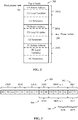
FIG. 2 illustrates an exemplarygeneral call stack 200. Thecall stack 200 may be used to store various information that may be used when a function is called. Each function that is pushed on the stack occupies a frame 202 as indicated by theframes - As a non-limiting example, each frame 202 of the
call stack 200 may include information such as parameters that are passed from the caller function to the called function. Thecall stack 200 may also include an area of memory for storing various local variables that may be used by the called program. A return address indicating where in the calling function execution should continue after the called function has completed execution may also be included in thecall stack 200. Thecall stack 200 operates as a Last In First Out (LIFO) buffer meaning that the last data pushed on the stack is the first data popped from the stack. Thecall stack 200 may be quite deep indicating that many function calls are nested within other functions. - A
frame pointer 204 generally points to the frame 202 of the currently operating function. Astack pointer 206 points to the next position of data on the stack that is available to be popped off and returned to a processor. - ROP exploits take advantage of the stack data structure by writing a malicious address to the return address portion of various frames 202. Operations related to the
call stack 200 that are corrupted by ROP exploits may be detected by one or more features and/or aspects discussed herein responsive to monitoring of cache activity, as is explained more fully below. -
FIG. 3 illustratesgadgets valid code sequence 300. Instructions are illustrated inFIG. 3 as including one or more bytes of instruction data. As non-limiting examples, a valid code sequences 300 (may also be referred to as an executable code sequence) includes a compare (CMP) instruction of 3 bytes, a shift right (SHR) instruction of 2 bytes, a load accumulator (LD A) instruction of 3 bytes, an add (ADD) instruction of 2 bytes, a move from register c to register (MOV a, c) instruction of 4 bytes, and a return (RET) instruction of 2 bytes. The instructions and encodings in the various bytes of the instructions shown inFIG. 3 are fabricated and not intended to be indicative of any specific instruction set. - Functions that may be called from other functions, generally end with a
return instruction 302. When the processor encounters thereturn instruction 302, it pops the top return address off the stack 200 (FIG. 2 ) to determine where execution should proceed. The top address on the stack should generally point to the address of the next instruction in the calling function after the call instruction in the calling function. However, in an attack using ROP exploits the return address may have been modified to point to a different address. - An attacker may identify the
gadget 304 that performs a particular function that may be useful to the attacker. Thegadget 304 ends with thereturn instruction 302 of thevalid code sequence 300. However, it will generally start somewhere within thevalid code sequence 300 to include useful instructions in front of thereturn instruction 302. Thus, thegadget 304 includes the add instruction followed by the move instruction followed by thereturn instruction 302. - Some instruction sets, such as Reduced Instruction Set Computer (RISC) instructions are generally fixed length, meaning that all the instructions are composed of the same number of bytes (e.g., 4 bytes). Other instructions sets, such as Complex Instruction Set Computer (RISC) instructions may vary in length as is illustrated in
FIG. 3 . With variable length instructions, the attacker has the opportunity to create new instructions that were not intended in the originalvalid code sequence 300. As a non-limiting example, thegadget 306 starts at a location within the move instruction of thevalid code sequences 300, which may create a subtract instruction if the processor starts execution at that point. Thus, thegadget 306 includes a subtract instruction followed by thereturn instruction 302. - An attacker may examine code that would be resident in memory, such as, for example, the standard C library, or portions of the operating system. The attacker can then identify many of these
gadget 304 and 306 (i.e., small code snippets) to create a library of ROP instructions. These ROP instruction may then be strung together to create a useful, unintended, and malicious code sequence without inserting any code into memory. Rather, the attacker only has to change return addresses on thecall stack 200 to point to the start of the desiredgadgets -
FIG. 4 illustrates an example of theprocessing system 100 including acache memory system 404. Theprocessing system 100 may include one ormore processors 402, thecache memory system 404, and themain memory 104.Various communication interfaces 424 and Input/Output (I/O) interfaces 426 may also be included. - As non-limiting examples, communication interfaces 424 may include interfaces for communication on cellular networks, serial ports, parallel ports, Ethernet connections, universal serial bus (USB) connections, IEEE 1394 ("firewire") connections, Bluetooth wireless connections, 802.1 a/b/g/n type wireless connections, and other suitable communication protocols and interfaces.
- As non-limiting examples, I/O interfaces 426 may include interfaces to devices such as keyboards, mice, trackballs, haptic devices, audio inputs and outputs, and displays.
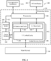
- A
cache monitor 414 is included to monitor whether various accesses to thecache memory system 404 are a "hit," meaning that the accessed data resides in thecache memory system 404 and is valid, or a "miss," meaning the desired location is not present in thecache memory system 404 or includes invalid data. Thus,bus 416 may indicate a miss or a hit, as well as other information, to thecache monitor 414. The cache monitor 414 may collect information such as a number of hits and a number of misses over a predefined time period or a predefined number of instruction fetches. Collected information about the hits and misses may be transmitted onbus 418 to aremedial action unit 420. Theremedial action unit 420 may process the hit and miss information and report results to theprocessor 402 overbus 422. As is explained more fully below the information collected and identified for theprocessor 402 may vary for different examples or implementations and may be as simple as a hit/miss ratio to more complex, such as an instruction loading profile. - The function of the
cache monitor 414, the function of theremedial action unit 420, or a combination thereof may be performed in hardware or software in different examples. - As a non-limiting example, one or more simple hardware counters in the cache monitor 414 may be used to keep track of cache hits, cache misses, or a combination thereof. The hardware counters may be cleared, preset, and read by software to control and analyze cache hit or miss information over specific time periods, specific number of instruction fetches, or a combination thereof. As one example, the
remedial action unit 420 could be configured to determine a hit/miss ratio or instruction loading profile under software control. Control may be based on a push-type model where the hardware generates an interrupt based on meeting certain criteria in hardware. For example, if a certain threshold number of misses or fetches are requested within a given time period, then the hardware may generate an interrupt. Control may also be based on a pull-type model where software may monitor the hardware registers relative to certain events such as elapsed time, context switch, and number of instructions fetched. In one example, the hardware registers may be checked on a periodic clock interrupt to ascertain whether an anomalous cache miss or instruction fetch condition is detected. - As another non-limiting example, more hardware could be included such as a threshold register or other profile information that could be set by a kernel or operating system based on expected behaviors for current operations. The hardware may then generate an interrupt when the hit/miss ratio exceeds or goes below the threshold register or profile information.
- In some examples, the
processor 402,cache memory system 404, cache monitor 414, andremedial action unit 420 may all be on the same semiconductor device orprocessing device 428. In other examples, thecache memory system 404 may be on a separate device from theprocessor 402. In such examples, thecache monitor 414 andremedial action unit 420 may be located with theprocessor 402, with thecache memory system 404, or split between the two devices. - Many
cache memory systems 404 include a multi-level cache including two ormore levels 412 of cache memory. The non-limiting example ofFIG. 4 illustrates a first level of cache including aseparate instruction cache 406 and adata cache 408. Separating instructions from data may create performance enhancements by creating parallel paths for fetching information and taking advantage of temporal and spatial proximity that may be different for instructions and data. A second level of cache is configured as aunified cache 410 including both instructions for theinstruction cache 406 and data for thedata cache 408. In addition, thecache memory system 404 may include different configuration for the caches, such as, for example set-associative caches and various replacement protocols for caches that are full, as would be known by a person of ordinary skill in the art of cache design. - Caches allow faster retrieval of instructions and data relative to having to go to the
main memory 104. The tradeoff compared to traditional memory is in size. In general, smaller memory has higher bandwidth, lower latency or a combination of both. Themain memory 104 is typically implemented as Dynamic Random Access Memory (DRAM), which can have relatively good bandwidth, but can have relatively long latencies. By caching frequently used data and instructions in a cache, fetches from theprocessor 402 can be received much more quickly and at a higher bandwidth. As a general rule,level 1 caches (i.e., caches closest to the processor 402) are smaller, faster, and have lower latency.Level 2 caches are generally larger, may be slower, and may have longer latencies. However, they are still faster thanmain memory 104 such that performance improvements are possible by including the second level of cache. - The
cache memory system 404 ofFIG. 4 is just one example. More of fewer levels may be used and each level may be implemented as aunified cache 410 orseparate instruction caches 406 anddata caches 408. Examples discussed herein are mostly concerned with instructions. As a result, discussions may refer specifically to theinstruction cache 406. However, a person of ordinary skill in the art will appreciate that these features may be practiced on any level of cache and in both theinstruction cache 406 and theunified cache 410. - Processors exploit properties of spatial and temporal proximity to optimize what is kept in the cache and what may have to be retrieved from the
main memory 104. For instance, frequently invoked code or functions may be kept in theinstruction cache 406. Also, it is common for functions or code in a page to invoke other nearby or spatially proximate code (e.g., within the same page). - However, such assumptions of proximity do not necessarily hold for ROP gadgets, since the fundamental property of ROP exploits is that they stitch together small segments of code located at distinct and seemingly random parts of the memory. This distribution of gadgets may result in a lot of "misses" for ROP exploits. In other words, the
processor 402 has to frequently load new lines into cache to find invoked gadgets. By contrast, the valid code sequences 300 (FIG. 3 ) may generally have far fewer misses and more "hits." In other words, a called function or code may be found in the same line already loaded in the cache. The different effects of ROP exploits on cache hit/miss characteristics compared to that of thevalid code sequences 300 can be exploited to build a detection mechanism that prevents ROP payloads from successfully executing. Such a system (that monitors hit/miss characteristics) can be trained to a specific operating system (OS) or process. - Some features or aspects of the present disclosure allow the detection of execution of ROP exploits at the lowest level possible, therefore they can be applied not only at process, but OS-level granularity. Moreover, the various aspects or features may not be tied to source code or compile-time modifications. Some examples of the present disclosure do not necessarily rely on preventing the attacker from reading any parts of the memory or directly controlling the flow of execution. All currently known mechanisms for mitigating ROP exploits (specifically, ASLR) routinely get circumvented because either an additional bug leaks the memory layout to the attacker or some part of the memory turns out to still be easily predictable, thus providing an attack surface to find ROP payloads. In contrast, the proposed method can detect an ROP exploit execution even if the attacker would have full knowledge of the memory map of the exploited processes.
-
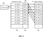
FIG. 5 illustrates details of an example of thecache memory system 404 ofFIG. 4 in a different context to explain operation of a cache as it relates to various aspects of the present disclosure. Theinstruction cache 406 includes a collection of lines with each line including anindex portion 502 and adata portion 504. The index portion includes a partial address (usually the most significant bits MSBs) such that different areas of memory with the same MSBs may be mapped to a specific line of theinstruction cache 406. Thus, as illustrated the cache line withindex 2 may containinstruction data 2 that originates frominstruction data 2A in themain memory 104 orinstruction data 2B in themain memory 104. Each cache line may be overwritten (i.e., replaced) with more recent instruction (i.e. temporally closer) if it is desired to load new instructions and there are no more cache lines available. - In operation, the
processor 402 requests a specific address to retrieve an instruction. If that address matches an index in a line of theinstruction cache 406, the instruction data (or a portion thereof) at the "hit" line is returned to theprocessor 402 as a cached instruction. If the requested address does not match any of the valid indexes in theinstruction cache 406, a "miss" occurs and theinstruction cache 406 fetches enough information from themain memory 104 including thenon-cached instruction 506 to fill a line of the cache and places the index for the requested addresses in the line of the cache. Subsequent requests to that cache line with that particular index will now generate hits to a cached instruction and there will be no need to fetch the instruction data from themain memory 104. - Long cache lines create spatial proximity and the ability to replace cache lines with more recently used data creates temporal proximity. Valid code sequences 300 (
FIG. 3 ) will generally have both good spatial proximity and good temporal proximity. On the other hand, ROP exploits will generally have poor spatial proximity and poor temporal proximity, due to the nature of the short snippets that may be located in many different areas of memory that are not necessarily accessed often. -
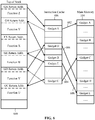
FIG. 6 illustrates an example of a corruptedcall stack 600 for generating a malicious code sequence including gadgets strung together to form a Return Oriented Programming (ROP) exploit. The corruptedcall stack 600 is in a corrupted form due to an attacker modifying one or more of the return addresses on the corruptedcall stack 600. Also illustrated inFIG. 6 are a portion of theinstruction cache 406 and a portion of themain memory 104. - With reference to
FIGS. 3 ,5 and6 , the corruptedcall stack 600 may include frames for functions U-Z. Solid arrows from the corruptedcall stack 600 to theinstruction cache 406 indicate return addresses popped off the stack causing theprocessor 402 to begin execution at the beginning of a particular gadget. Dashed arrows from theinstruction cache 406 to the corruptedcall stack 600 indicate return instruction executed at the end of the particular gadget to fetch the return address from the stack. - In the corrupted
call stack 600, the return address for function Z has been modified to point to a start address of gadget A. Similarly, the return address for function Y has been modified to point to a start address of gadget B, the return address for function W has been modified to point to a start address of gadget E, the return address for function V has been modified to point to a start address of gadget D, and the return address for function U has been modified to point to a start address of gadget C. The return address for function X has not been modified. - Because of these modifications, when function Z completes its operation and the
return instruction 302 is performed, rather than return to the proper place, control continues at the beginning of gadget A, for which the address has been placed in the return address of function Z. Every gadget ends with areturn instruction 302. Thus, when gadget A completes itsreturn instruction 302 points to the return address of function Y. However, the return address of function Y has been modified to point to the beginning of gadget B. As a result, rather than return to the proper place, control continues at the beginning of gadget B. Continuing with the gadget executions, after gadget B completes, rather than return to the proper place for function U, control continues at the beginning of gadget C. After gadget C completes, rather than return to the proper place for function V, control continues at the beginning of gadget D. After gadget D completes, rather than return to the proper place for function W, control continues at the beginning of gadget E. This stringing together of gadgets A-E can perform significant functions forming at least a part of an ROP exploit. - However, because these gadgets A-E may exist at diverse addresses, they may cause a larger number of cache misses than if program execution had happened normally. In the non-limiting example of
FIG. 6 , gadget A is not located in theinstruction cache 406 causing a miss and the need to fetch thenon-cached code snippet 602 from themain memory 104. Similarly, gadgets C, D, and E miss theinstruction cache 406 causing fetches ofnon-cached code snippets main memory 104. The fetch of gadget B caused a hit allowing return of a cached code snippet for gadget B. - With longer ROP exploit payloads made up of more code snippets, the trend of a larger than expected number of misses relative to hits becomes more apparent and confidence is increased that an ROP exploit may be the cause.
-
FIG. 7 is a flow diagram showing anexemplary process 700 to detect anomalous miss activity for the cache memory to detect and terminate an ROP exploit.Process 700 will be described with reference toFIGS. 7 and4 . Inoperation block 702, the process includes loading an executable code sequence in the cache memory. In other words, at least some of the cache lines are loaded with at least portions of executable code sequences. Inoperation block 704, theprocessor 402 perform instruction fetches of the executable code sequences from the cache memory, which may include cache hits and cache misses. These code sequences may be valid code sequences or they may be a series of gadgets forming an ROP exploit payload. - In
operation block 706, the cache monitor 414 alone, in combination with theremedial action unit 420, or in combination with both theremedial action unit 420 and theprocessor 402, monitors the instruction fetches relative to cache misses to dynamically determine if there is anomalous miss activity, wherein cache misses are fetched instructions absent from the cache memory on the instruction fetch. The instruction fetches are monitored dynamically during execution of the instructions rather than monitoring instruction fetches in an effort to predetermine cache hit/miss behavior relative to a specific instruction sequence. The anomalous miss activity may be determined by different metrics. Some non-limiting metrics are the number of cache hits relative to the number of cache misses to develop a hit/miss ratio, the number of cache misses relative to the number of instruction fetches, the number of cache misses over a certain time period, or the number of cache misses over an expected code sequence. As a non-limiting example, this hit/miss ratio may be a moving average as instructions are fetched. Of course, a hit/miss ratio may be conversely expressed as a miss/hit ratio. - In some examples, a certain predefined number of instruction fetches may be desired to determine the anomalous miss activity.
Decision block 708 indicates that a test occurs to see if the desired number of fetches has been reached. If not, control returns to operation block 704 as more instructions are fetched and executed. As non-limiting examples, the desired number of fetches may be set at numbers such as 10, 50, and 100 instructions. In addition, the desired number of fetches may be determined over a predefined time period. As another non-limiting example the desired number of fetches may be correlated to a predetermined operating context such as execution of specific software programs, specific software libraries, or specific operating system operations. - If enough instruction fetches have occurred,
decision block 710 indicates a test to see if the anomalous miss activity, which may be defined as a hit/miss ratio below a threshold. If not, valid code sequences are likely being executed and control returns to operation block 704 to monitor more instruction fetches. - If there is anomalous miss activity, it is likely that an ROP exploit is executing and
operation block 712 indicates that the anomalous miss activity miss activity may be reported such that remedial action may be taken relative to the executable code sequence. As explained earlier, the reporting may be to theremedial action unit 420, or to theprocessor 402. -
Operation block 714 indicates that one type of remedial measure that may be performed would be to terminate execution of the executable code sequence in response to the reporting of the anomalous miss activity. This termination may terminate many different ways, such as, for example, creating a hardware or software exception or creating a hardware or software interrupt. - The threshold may be selected to be lower than typical hit/miss ratios for valid code sequences. For instance, the hit/miss threshold may be empirically selected for each operating system and/or processor type.
- Moreover, there may be periods of execution, or execution of certain types of valid code sequences, where a larger number of misses may be expected, such as, for example, during a boot up stage where the caches have not yet been loaded with valid instructions or particular valid code sequences that may cause cache trashing. Thus, there may be selected operational periods, such as during initial boot-up of a
processor 402 or operating system when the monitoring acts may be suspended. If these types of events are known, more complex instruction loading profiles may be developed for both valid code sequences and ROP exploits. -
Operation block 716 indicates that the process may also determine that the anomalous miss activity is indicative of a return-oriented programming exploit. While illustrated at the end, if the act ofoperation block 716 is performed, it may be performed earlier in the process in a manner thatoperations -
FIG. 8 is a flow diagram showing anexemplary process 800 to develop an instruction loading profile and perform remedial actions responsive to the analysis of the instruction loading profile.Process 800 will be described with reference toFIGS. 8 and4 .Operation block 802 indicates that the process executes an unintended sequence of code snippets in aprocessing circuit 402, each code snippet comprising at least one executable instruction including a control transfer instruction. At least one code snippet of the plurality is a non-cached code snippet not found in a cache memory. The process executes an unintended code sequence because one or more of the code snippets includes a modified control transfer instruction different from an originally intended control transfer instruction. As non-limiting examples, a control transfer instruction may be instructions such as jump instructions, return instructions, and branch instructions. Thus, an originally intended control transfer function is, for example, a return instruction that was originally placed on the call stack as the valid program intended. In an ROP exploit, the originally intended control transfer function may be changed to a modified control transfer instruction to perform a different function resulting in the unintended sequence of code snippets. -
Operation block 804 indicates that the process develops an instruction loading profile by monitoring the instruction fetches relative to cache misses, where the cache misses are fetched instructions absent from the cache memory on the instruction fetch. In other words, cache hits and cache misses are monitored during execution of valid code sequences and code snippets. As these instruction fetches occur, an instruction loading profile may be developed. The instruction loading profile may be quite complex and track events and actions such as for example temporal separation and spatial separation between cache misses and may even track replacement of cache line indexes to indicate if certain cache lines are more likely to be involved in ROP exploits. On the other hand, the instruction loading profile may be as simple as the hit/miss ratio discussed above with reference toFIG. 7 . -
Operation block 806 indicates that the instruction loading profile may be developed as a hit/miss ratio of fetches of cached instructions relative to non-cached instructions. The operation may monitor to see if the hit/miss ratio is lower than a threshold that may be determined or selected relative to valid hit/miss ratios indicative of valid code sequences. -
Operation block 808 indicates that the valid hit/miss ratios may be determined from monitoring hit/miss ratios from a plurality of executable code sequences known to be free from the return-oriented programming exploit during monitoring the hit/miss ratios, as is explained more fully below with reference toFIG. 9 . -
Decision block 810 indicates that a test may be performed to see if the current instruction loading profile is similar to an instruction loading profile of an ROP exploit. If not, control may return to operation block 804 to monitor additional instruction fetches and whether they cause cache hits or cache misses. - If the current instruction loading profile is similar to an instruction loading profile of an ROP exploit,
operation block 812 indicates that remedial actions relative to the executable code sequences may be performed if the instruction loading profile is indicative of execution of a return-oriented programming exploit involving one or more of the executable code sequences. As a non-limiting example, a remedial action may be terminating execution of at least one code snippet of the sequence if the instruction loading profile is indicative of execution of some of the code snippets of the sequence above with reference toFIG. 7 . - Profiles for both valid code sequences and ROP exploits may be developed ahead of time in a test environment for use during normal operation.
-
FIG. 9 is a flow diagram showing anexemplary process 900 to develop information about execution of valid code sequences and ROP exploits for use in analyzing instruction loading profiles.Process 900 will be described with reference toFIGS. 9 and4 . Inoperation block 902, valid test code sequences are executed. Inoperation block 904, cache hits and cache misses are monitored for the valid test code sequences. In one example, a valid hit/miss ratio may be developed from execution of the valid test code sequences.Operation block 906 indicates that various instruction loading profiles can be developed for valid code sequences. In this way, valid code sequences that may have a relatively low hit/miss ratio may still have other hit/miss characteristics that would identify them as valid code sequences rather than ROP exploits. Operation blocks 902, 904, and 906 may be repeated for any number of valid code sequences that might be of interest. - In
operation block 908, test ROP exploit sequences are executed. Inoperation block 910, cache hits and cache misses are monitored for the test ROP exploit sequences.Operation block 912 indicates that various instruction loading profiles can be developed for the test ROP exploit sequences. Because attackers can be quite creative and do unexpected things, developing test ROP exploit sequences may be more difficult than identifying valid code sequences of interest. However, the development of instruction loading profiles for at least some ROP exploits may help thecache monitor 414,remedial action unit 420, andprocessor 402 make more informed decisions on whether an ROP exploit is executing. - Returning to
FIG. 8 , with instruction loading profiles for bothvalid code sequences 300 and ROP exploits,decision block 808 may be expanded to test whether the current instruction loading profile is similar to an ROP exploit or dissimilar from a valid code sequence. - It should be pointed out that the processed discussed herein relative to
FIGS. 7 ,8 , and9 are processes related to detecting ROP exploits by monitoring thecache memory system 404 and are not necessarily processes related to execution of software programs running on theprocessing system 100. - Specific implementations shown and described are only examples and should not be construed as the only way to implement the present disclosure unless specified otherwise herein. It is readily apparent to one of ordinary skill in the art that the various examples in the present disclosure may be practiced by numerous other partitioning solutions.
- One or more of the components, acts, features and/or functions described herein and illustrated in the drawings may be rearranged and/or combined into a single component, act, feature, or function or embodied in several components, acts, features, or functions. Additional elements, components, acts, and/or functions may also be added without departing from the various features and/or aspects described herein. The algorithms described herein may also be efficiently implemented in software and/or embedded in hardware.
- In the description, elements, circuits, and functions may be shown in block diagram form in order not to obscure the present disclosure in unnecessary detail. Conversely, specific implementations shown and described are exemplary only and should not be construed as the only way to implement the present disclosure unless specified otherwise herein. Additionally, block definitions and partitioning of logic between various blocks is exemplary of a specific implementation. It is readily apparent to one of ordinary skill in the art that the present disclosure may be practiced by numerous other partitioning solutions. For the most part, details concerning timing considerations and the like have been omitted where such details are not necessary to obtain a complete understanding of the present disclosure and are within the abilities of persons of ordinary skill in the relevant art.
- Also, it is noted that the examples may be described as a process that is depicted as a flowchart, a flow diagram, a structure diagram, or a block diagram. Although a flowchart may describe the operations as a sequential process, many of the operations can be performed in parallel or concurrently. In addition, the order of the operations may be re-arranged. A process is terminated when its operations are completed. A process may correspond to a method, a function, a procedure, a subroutine, a subprogram, etc. When a process corresponds to a function, its termination corresponds to a return of the function to the calling function or the main function.
- Those of ordinary skill in the art would understand that information and signals may be represented using any of a variety of different technologies and techniques. For example, data, instructions, commands, information, signals, bits, symbols, and chips that may be referenced throughout this description may be represented by voltages, currents, electromagnetic waves, magnetic fields or particles, optical fields or particles, or any combination thereof. Some drawings may illustrate signals as a single signal for clarity of presentation and description. It will be understood by a person of ordinary skill in the art that the signal may represent a bus of signals, wherein the bus may have a variety of bit widths and the present disclosure may be implemented on any number of data signals, including a single data signal.
- Elements described herein may include multiple instances of the same element. These elements may be generically indicated by a numerical designator (e.g. 110) and specifically indicated by the numerical indicator followed by an alphabetic designator (e.g., 110A) or a numeric indicator preceded by a "dash" (e.g., 110-1). For ease of following the description, for the most part element number indicators begin with the number of the drawing on which the elements are introduced or most fully discussed.
- It should be understood that any reference to an element herein using a designation such as "first," "second," and so forth does not limit the quantity or order of those elements, unless such limitation is explicitly stated. Rather, these designations may be used herein as a convenient method of distinguishing between two or more elements or instances of an element. Thus, a reference to first and second elements does not mean that only two elements may be employed there or that the first element must precede the second element in some manner. In addition, unless stated otherwise, a set of elements may comprise one or more elements.
- Moreover, a storage medium may represent one or more devices for storing data, including read-only memory (ROM), random access memory (RAM), magnetic disk storage mediums, optical storage mediums, flash memory devices and/or other machine-readable mediums and, processor-readable mediums, and/or computer-readable mediums for storing information. The terms "machine-readable medium," "computer-readable medium," and/or "processor-readable medium" may include, but are not limited to non-transitory mediums such as portable or fixed storage devices, optical storage devices, and various other mediums capable of storing, containing or carrying instruction(s) and/or data. Thus, the various methods described herein may be fully or partially implemented by instructions and/or data that may be stored in a "machine-readable medium," "computer-readable medium," and/or "processor-readable medium" and executed by one or more processors, machines and/or devices.
- Furthermore, various features and/or aspects may be implemented in hardware, software, firmware, middleware, microcode, or any combination thereof. When implemented in software, firmware, middleware or microcode, the program code or code segments to perform the necessary tasks may be stored in a machine-readable medium such as a storage medium or other storage(s). A processor may perform the necessary tasks. A code segment may represent a procedure, a function, a subprogram, a program, a routine, a subroutine, a module, a software package, a class, or any combination of instructions, data structures, or program statements. A code segment may be coupled to another code segment or a hardware circuit by passing and/or receiving information, data, arguments, parameters, or memory contents. Information, arguments, parameters, data, etc. may be passed, forwarded, or transmitted via any suitable means including memory sharing, message passing, token passing, network transmission, etc.
- The various illustrative logical blocks, modules, circuits, elements, and/or components described in connection with the examples disclosed herein may be implemented or performed with a general purpose processor, a digital signal processor (DSP), an application specific integrated circuit (ASIC), a field programmable gate array (FPGA) or other programmable logic component, discrete gate or transistor logic, discrete hardware components, or any combination thereof designed to perform the functions described herein. A general-purpose processor may be a microprocessor, but in the alternative, the processor may be any conventional processor, controller, microcontroller, or state machine. A processor may also be implemented as a combination of computing components, e.g., a combination of a DSP and a microprocessor, a number of microprocessors, one or more microprocessors in conjunction with a DSP core, or any other such configuration. A general-purpose processor, configured for executing features described herein, may be considered a special purpose processor for carrying out such features. Similarly, a general-purpose computer may be considered a special purpose computer when configured for carrying out features described herein.
- The methods or algorithms described in connection with the examples disclosed herein may be embodied directly in hardware, in a software module executable by a processor, or in a combination of both, in the form of processing unit, programming instructions, or other directions, and may be contained in a single device or distributed across multiple devices. A software module may reside in RAM memory, flash memory, ROM memory, EPROM memory, EEPROM memory, registers, hard disk, a removable disk, a CD-ROM, or any other form of storage medium known in the art. A storage medium may be coupled to the processor such that the processor can read information from, and write information to, the storage medium. In the alternative, the storage medium may be integral to the processor.
- Those of skill in the art would further appreciate that the various illustrative logical blocks, modules, circuits, and algorithm steps described in connection with the examples and features disclosed herein may be implemented as electronic hardware, computer software, or combinations of both. To clearly illustrate this interchangeability of hardware and software, various illustrative components, blocks, modules, circuits, and steps have been described above generally in terms of their functionality. Whether such functionality is implemented as hardware, software, or a combination thereof depends upon the particular application and design selections imposed on the overall system.
- The various features described herein can be implemented in different systems. It should be noted that the foregoing examples and are not to be construed as limiting. The description of the examples is intended to be illustrative, and not to limit the scope of the claims. As such, the present teachings can be readily applied to other types of apparatuses and many alternatives, modifications, and variations will be apparent to those skilled in the art.
Claims (10)
- A method operational in a processing circuit including cache memory, comprising:loading at least portions of an executable code sequence in the cache memory;performing instruction fetches of the executable code sequence from the cache memory;detecting one or more instruction fetch cache misses in response to the instruction fetches, where an individual instruction fetch cache miss represents a fetched instruction absent from the cache memory; andmonitoring the instruction fetches relative to the one or more instruction fetch cache misses in order to dynamically detect anomalous instruction fetch cache miss activity.
- The method of claim 1, further comprising:
reporting the anomalous miss activity and, in response to the anomalous miss activity, performing a remedial action relative to the executable code sequence. - The method of claim 2, further comprising:
performing the remedial action by terminating execution of the executable code sequence responsive to the reporting of the anomalous miss activity. - The method of claim 1, wherein monitoring the instruction fetches relative to cache misses includes
detecting one or more instruction fetch cache hits in response to the instruction fetches;
determining an instruction fetch cache hit/miss ratio in response to the detected instruction fetch cache hits and instruction fetch cache misses; and
detecting anomalous instruction fetch cache miss activity by detecting a hit/miss ratio lower than a threshold selected relative to valid hit/miss ratios indicative of valid code sequences. - The method of claim 4, wherein the valid hit/miss ratios are determined from monitoring instruction fetch cache hit/miss ratios from a plurality of the executable code sequences that are free from a return-oriented programming exploit during the monitoring.
- The method of claim 1, wherein the monitoring is suspended during a selected operational period.
- The method of claim 6, wherein the selected operational period includes a boot-up stage of a new process.
- The method of claim 1, wherein the anomalous miss activity is determined over a predefined number of preceding instructions or a predefined time period.
- A processing device, comprising:means for loading at least portions of an executable code sequence in a cache memory;means for performing instruction fetches of the executable code sequence from the cache memory;means for detecting one or more instruction fetch cache misses in response to the instruction fetches, where an individual instruction fetch cache miss represents a fetched instruction absent from the cache memory ; andmeans for monitoring the instruction fetches relative to the one or more instruction fetch cache misses in order to dynamically detect anomalous instruction fetch cache miss activity.
- A non-transitory machine-readable medium having instructions stored thereon, which when executed by a processing device according to claim 9 cause the processing device of a computer to:load at least portions of an executable code sequence in a cache memory;perform instruction fetches of the executable code sequence from the cache memory; anddetect one or more instruction fetch cache misses in response to the instruction fetches, where an individual instruction fetch cache miss represents a fetched instruction absent from the cache memory; andmonitor the instruction fetches relative to the one or more instruction fetch cache misses in order to dynamically detect anomalous instruction fetch cache miss activity.
Priority Applications (1)
| Application Number | Priority Date | Filing Date | Title |
|---|---|---|---|
| EP16163454.8A EP3062259A1 (en) | 2011-11-07 | 2012-11-07 | Methods, devices, and systems for detecting return-oriented programming exploits |
Applications Claiming Priority (2)
| Application Number | Priority Date | Filing Date | Title |
|---|---|---|---|
| US13/290,932 US8839429B2 (en) | 2011-11-07 | 2011-11-07 | Methods, devices, and systems for detecting return-oriented programming exploits |
| PCT/US2012/063953 WO2013070773A2 (en) | 2011-11-07 | 2012-11-07 | Methods, devices, and systems for detecting return-oriented programming exploits |
Related Child Applications (2)
| Application Number | Title | Priority Date | Filing Date |
|---|---|---|---|
| EP16163454.8A Division-Into EP3062259A1 (en) | 2011-11-07 | 2012-11-07 | Methods, devices, and systems for detecting return-oriented programming exploits |
| EP16163454.8A Division EP3062259A1 (en) | 2011-11-07 | 2012-11-07 | Methods, devices, and systems for detecting return-oriented programming exploits |
Publications (2)
| Publication Number | Publication Date |
|---|---|
| EP2776971A2 EP2776971A2 (en) | 2014-09-17 |
| EP2776971B1 true EP2776971B1 (en) | 2019-01-16 |
Family
ID=47428964
Family Applications (2)
| Application Number | Title | Priority Date | Filing Date |
|---|---|---|---|
| EP16163454.8A Withdrawn EP3062259A1 (en) | 2011-11-07 | 2012-11-07 | Methods, devices, and systems for detecting return-oriented programming exploits |
| EP12805807.0A Not-in-force EP2776971B1 (en) | 2011-11-07 | 2012-11-07 | Methods, devices, and systems for detecting return-oriented programming exploits |
Family Applications Before (1)
| Application Number | Title | Priority Date | Filing Date |
|---|---|---|---|
| EP16163454.8A Withdrawn EP3062259A1 (en) | 2011-11-07 | 2012-11-07 | Methods, devices, and systems for detecting return-oriented programming exploits |
Country Status (6)
| Country | Link |
|---|---|
| US (2) | US8839429B2 (en) |
| EP (2) | EP3062259A1 (en) |
| JP (1) | JP5944520B2 (en) |
| CN (1) | CN103946855B (en) |
| IN (1) | IN2014CN03071A (en) |
| WO (1) | WO2013070773A2 (en) |
Families Citing this family (43)
| Publication number | Priority date | Publication date | Assignee | Title |
|---|---|---|---|---|
| US9268945B2 (en) * | 2010-03-19 | 2016-02-23 | Contrast Security, Llc | Detection of vulnerabilities in computer systems |
| US8839429B2 (en) | 2011-11-07 | 2014-09-16 | Qualcomm Incorporated | Methods, devices, and systems for detecting return-oriented programming exploits |
| WO2013106594A1 (en) * | 2012-01-10 | 2013-07-18 | Telcordia Technologies, Inc. | Adaptive-diversity for compressible return oriented programs |
| US9256730B2 (en) * | 2012-09-07 | 2016-02-09 | Crowdstrike, Inc. | Threat detection for return oriented programming |
| US9177147B2 (en) * | 2012-09-28 | 2015-11-03 | Intel Corporation | Protection against return oriented programming attacks |
| US9223979B2 (en) * | 2012-10-31 | 2015-12-29 | Intel Corporation | Detection of return oriented programming attacks |
| US10114643B2 (en) | 2013-05-23 | 2018-10-30 | Intel Corporation | Techniques for detecting return-oriented programming |
| US10310863B1 (en) * | 2013-07-31 | 2019-06-04 | Red Hat, Inc. | Patching functions in use on a running computer system |
| US9292684B2 (en) | 2013-09-06 | 2016-03-22 | Michael Guidry | Systems and methods for security in computer systems |
| US9465936B2 (en) | 2013-11-06 | 2016-10-11 | Bitdefender IPR Management Ltd. | Systems and methods for detecting return-oriented programming (ROP) exploits |
| US9928110B2 (en) * | 2014-03-31 | 2018-03-27 | Cfph, Llc | Resource allocation based on processor assignments |
| US9390264B2 (en) | 2014-04-18 | 2016-07-12 | Qualcomm Incorporated | Hardware-based stack control information protection |
| US20160196427A1 (en) * | 2014-07-08 | 2016-07-07 | Leviathan, Inc. | System and Method for Detecting Branch Oriented Programming Anomalies |
| US9904780B2 (en) * | 2014-07-31 | 2018-02-27 | Nec Corporation | Transparent detection and extraction of return-oriented-programming attacks |
| US9589133B2 (en) * | 2014-08-08 | 2017-03-07 | International Business Machines Corporation | Preventing return-oriented programming exploits |
| CN104268471B (en) * | 2014-09-10 | 2017-04-26 | 珠海市君天电子科技有限公司 | Method and device for detecting return-oriented programming attack |
| EP2996034B1 (en) * | 2014-09-11 | 2018-08-15 | Nxp B.V. | Execution flow protection in microcontrollers |
| US9519773B2 (en) * | 2014-09-12 | 2016-12-13 | Intel Corporation | Returning to a control transfer instruction |
| EP3195177A1 (en) * | 2014-09-17 | 2017-07-26 | Irdeto B.V. | Generating and executing protected items of software |
| US9465938B2 (en) * | 2014-09-22 | 2016-10-11 | Qualcomm Incorporated | Integrated circuit and method for detection of malicious code in a first level instruction cache |
| US9501637B2 (en) * | 2014-09-26 | 2016-11-22 | Intel Corporation | Hardware shadow stack support for legacy guests |
| US9646154B2 (en) * | 2014-12-12 | 2017-05-09 | Microsoft Technology Licensing, Llc | Return oriented programming (ROP) attack protection |
| US9940484B2 (en) * | 2014-12-23 | 2018-04-10 | Intel Corporation | Techniques for detecting false positive return-oriented programming attacks |
| CN104732139A (en) * | 2015-02-04 | 2015-06-24 | 深圳市中兴移动通信有限公司 | Internal storage monitoring method and terminal |
| SG10201500921QA (en) * | 2015-02-06 | 2016-09-29 | Huawei Internat Pte Ltd | Method for obfuscation of code using return oriented programming |
| US9842209B2 (en) * | 2015-05-08 | 2017-12-12 | Mcafee, Llc | Hardened event counters for anomaly detection |
| SG10201504066QA (en) * | 2015-05-25 | 2016-12-29 | Huawei Internat Pte Ltd | Method and system for defense against return oriented programming (rop) based attacks |
| US11227056B2 (en) | 2015-08-18 | 2022-01-18 | The Trustees Of Columbia University In The City Of New York | Inhibiting memory disclosure attacks using destructive code reads |
| US10019572B1 (en) * | 2015-08-27 | 2018-07-10 | Amazon Technologies, Inc. | Detecting malicious activities by imported software packages |
| US10032031B1 (en) | 2015-08-27 | 2018-07-24 | Amazon Technologies, Inc. | Detecting unknown software vulnerabilities and system compromises |
| US10282224B2 (en) | 2015-09-22 | 2019-05-07 | Qualcomm Incorporated | Dynamic register virtualization |
| US20170091454A1 (en) * | 2015-09-25 | 2017-03-30 | Vadim Sukhomlinov | Lbr-based rop/jop exploit detection |
| US9576138B1 (en) | 2015-09-30 | 2017-02-21 | International Business Machines Corporation | Mitigating ROP attacks |
| US9767292B2 (en) | 2015-10-11 | 2017-09-19 | Unexploitable Holdings Llc | Systems and methods to identify security exploits by generating a type based self-assembling indirect control flow graph |
| US10437998B2 (en) | 2015-10-26 | 2019-10-08 | Mcafee, Llc | Hardware heuristic-driven binary translation-based execution analysis for return-oriented programming malware detection |
| US10419423B2 (en) | 2015-10-30 | 2019-09-17 | Mcafee, Llc | Techniques for identification of location of relevant fields in a credential-seeking web page |
| US10878091B2 (en) * | 2016-02-24 | 2020-12-29 | Nippon Telegraph And Telephone Corporation | Attack code detection device, attack code detection method, and attack code detection program |
| US10423792B2 (en) | 2016-09-23 | 2019-09-24 | Red Hat, Inc. | Identifying exploitable code sequences |
| US10437990B2 (en) | 2016-09-30 | 2019-10-08 | Mcafee, Llc | Detection of return oriented programming attacks in a processor |
| US10489592B1 (en) * | 2017-03-21 | 2019-11-26 | Symantec Corporation | Creating an execution safety container for unreliable exploits |
| DE102017124805B4 (en) * | 2017-10-24 | 2019-05-29 | Infineon Technologies Ag | MEMORY ARRANGEMENT AND METHOD FOR INTERMEDIATELY STORING MEMORY CONTENT |
| CN112395598B (en) * | 2019-08-15 | 2024-04-19 | 奇安信安全技术(珠海)有限公司 | Protection method, device and equipment for damaged instruction execution sequence |
| US11445225B2 (en) * | 2020-10-27 | 2022-09-13 | Akamai Technologies, Inc. | Measuring and improving origin offload and resource utilization in caching systems |
Family Cites Families (24)
| Publication number | Priority date | Publication date | Assignee | Title |
|---|---|---|---|---|
| US5956477A (en) * | 1996-11-25 | 1999-09-21 | Hewlett-Packard Company | Method for processing information in a microprocessor to facilitate debug and performance monitoring |
| US6047363A (en) * | 1997-10-14 | 2000-04-04 | Advanced Micro Devices, Inc. | Prefetching data using profile of cache misses from earlier code executions |
| US6134710A (en) * | 1998-06-26 | 2000-10-17 | International Business Machines Corp. | Adaptive method and system to minimize the effect of long cache misses |
| EP1331539B1 (en) | 2002-01-16 | 2016-09-28 | Texas Instruments France | Secure mode for processors supporting MMU and interrupts |
| US7086088B2 (en) * | 2002-05-15 | 2006-08-01 | Nokia, Inc. | Preventing stack buffer overflow attacks |
| JP4086846B2 (en) * | 2002-11-13 | 2008-05-14 | 富士通株式会社 | Scheduling method and multi-threading processor in multi-threading processor |
| US7954102B2 (en) | 2002-11-13 | 2011-05-31 | Fujitsu Limited | Scheduling method in multithreading processor, and multithreading processor |
| GB0226875D0 (en) * | 2002-11-18 | 2002-12-24 | Advanced Risc Mach Ltd | Control of access to a memory by a device |
| US7134029B2 (en) | 2003-11-06 | 2006-11-07 | International Business Machines Corporation | Computer-component power-consumption monitoring and control |
| US7392370B2 (en) | 2004-01-14 | 2008-06-24 | International Business Machines Corporation | Method and apparatus for autonomically initiating measurement of secondary metrics based on hardware counter values for primary metrics |
| KR100586500B1 (en) | 2004-03-18 | 2006-06-07 | 학교법인고려중앙학원 | Method for sensing and recovery against buffer overflow attacks and apparatus thereof |
| FR2877118B1 (en) * | 2004-10-22 | 2007-01-19 | Oberthur Card Syst Sa | PROTECTION AGAINST ATTACKS BY GENERATING FAULTS ON JUMPING INSTRUCTIONS |
| US7730531B2 (en) | 2005-04-15 | 2010-06-01 | Microsoft Corporation | System and method for detection of artificially generated system load |
| US7818747B1 (en) | 2005-11-03 | 2010-10-19 | Oracle America, Inc. | Cache-aware scheduling for a chip multithreading processor |
| US20070150881A1 (en) * | 2005-12-22 | 2007-06-28 | Motorola, Inc. | Method and system for run-time cache logging |
| JP4915774B2 (en) | 2006-03-15 | 2012-04-11 | 株式会社日立製作所 | Storage system and storage system control method |
| US20080263324A1 (en) | 2006-08-10 | 2008-10-23 | Sehat Sutardja | Dynamic core switching |
| US8447962B2 (en) * | 2009-12-22 | 2013-05-21 | Intel Corporation | Gathering and scattering multiple data elements |
| JP2009217385A (en) * | 2008-03-07 | 2009-09-24 | Toshiba Corp | Processor and multiprocessor |
| US8490061B2 (en) * | 2009-05-07 | 2013-07-16 | International Business Machines Corporation | Profiling application performance according to data structure |
| US8689201B2 (en) * | 2010-01-27 | 2014-04-01 | Telcordia Technologies, Inc. | Automated diversity using return oriented programming |
| CN101924761B (en) | 2010-08-18 | 2013-11-06 | 北京奇虎科技有限公司 | Method for detecting malicious program according to white list |
| US8997218B2 (en) * | 2010-12-22 | 2015-03-31 | F-Secure Corporation | Detecting a return-oriented programming exploit |
| US8839429B2 (en) | 2011-11-07 | 2014-09-16 | Qualcomm Incorporated | Methods, devices, and systems for detecting return-oriented programming exploits |
-
2011
- 2011-11-07 US US13/290,932 patent/US8839429B2/en not_active Expired - Fee Related
-
2012
- 2012-11-07 IN IN3071CHN2014 patent/IN2014CN03071A/en unknown
- 2012-11-07 CN CN201280054578.4A patent/CN103946855B/en active Active
- 2012-11-07 JP JP2014540222A patent/JP5944520B2/en not_active Expired - Fee Related
- 2012-11-07 EP EP16163454.8A patent/EP3062259A1/en not_active Withdrawn
- 2012-11-07 EP EP12805807.0A patent/EP2776971B1/en not_active Not-in-force
- 2012-11-07 WO PCT/US2012/063953 patent/WO2013070773A2/en active Application Filing
-
2014
- 2014-08-29 US US14/473,736 patent/US9262627B2/en active Active
Non-Patent Citations (1)
| Title |
|---|
| LIWEI YUAN ET AL: "Security Breaches as PMU Deviation: Detecting and Identifying Security Attacks Using Performance Counters", PROCEEDINGS OF THE SECOND ASIA-PACIFIC WORKSHOP ON SYSTEMS, APSYS '11, 11 July 2011 (2011-07-11), New York, New York, USA, XP055146897, ISBN: 978-1-45-031179-3, Retrieved from the Internet <URL:10.1145/2103799.2103807> [retrieved on 20141015], DOI: 10.1145/2103799.2103807 * |
Also Published As
| Publication number | Publication date |
|---|---|
| US9262627B2 (en) | 2016-02-16 |
| JP2014532944A (en) | 2014-12-08 |
| IN2014CN03071A (en) | 2015-07-31 |
| US20130117843A1 (en) | 2013-05-09 |
| EP2776971A2 (en) | 2014-09-17 |
| WO2013070773A3 (en) | 2013-12-12 |
| JP5944520B2 (en) | 2016-07-05 |
| WO2013070773A2 (en) | 2013-05-16 |
| CN103946855A (en) | 2014-07-23 |
| EP3062259A1 (en) | 2016-08-31 |
| US8839429B2 (en) | 2014-09-16 |
| CN103946855B (en) | 2017-03-08 |
| US20140372701A1 (en) | 2014-12-18 |
Similar Documents
| Publication | Publication Date | Title |
|---|---|---|
| EP2776971B1 (en) | Methods, devices, and systems for detecting return-oriented programming exploits | |
| EP2805246B1 (en) | Dynamic execution prevention to inhibit return-oriented programming | |
| Venkataramani et al. | Memtracker: Efficient and programmable support for memory access monitoring and debugging | |
| JP6185487B2 (en) | Keeping secure data isolated from non-secure access when switching between domains | |
| US9495541B2 (en) | Detecting return-oriented programming payloads by evaluating data for a gadget address space address and determining whether operations associated with instructions beginning at the address indicate a return-oriented programming payload | |
| CN109508536B (en) | Detection method and device for tampering program flow attack | |
| US10565379B2 (en) | System, apparatus and method for instruction level behavioral analysis without binary instrumentation | |
| Irazoqui et al. | MASCAT: Stopping microarchitectural attacks before execution | |
| US10984096B2 (en) | Systems, methods, and apparatus for detecting control flow attacks | |
| US20120179898A1 (en) | System and method for enforcing software security through cpu statistics gathered using hardware features | |
| CN110032867B (en) | Method and system for actively cutting off hidden channel to deal with channel attack at cache side | |
| CN109643346B (en) | Control flow integrity | |
| Zhao et al. | Speculation invariance (invarspec): Faster safe execution through program analysis | |
| US7971031B2 (en) | Data processing system and method | |
| US20170091454A1 (en) | Lbr-based rop/jop exploit detection | |
| US20110066897A1 (en) | Methods and apparatuses for determining permanent memory growth | |
| CN112541178A (en) | Apparatus and method for control flow integrity enforcement | |
| US20210349995A1 (en) | Systems and Methods for Protecting Cache and Main-Memory from Flush-Based Attacks | |
| Omotosho et al. | Detecting return-oriented programming on firmware-only embedded devices using hardware performance counters | |
| US20220335135A1 (en) | Vulnerability analysis and reporting for embedded systems | |
| Aimoniotis et al. | Data-Out Instruction-In (DOIN!): Leveraging Inclusive Caches to Attack Speculative Delay Schemes | |
| US20180004947A1 (en) | Enhanced control transfer security | |
| Taheri et al. | Comprehensive evaluation of rsb and spectre vulnerability on modern processors | |
| Chen et al. | Exploration for software mitigation to spectre attacks of poisoning indirect branches | |
| Coronado | On the Balance Between the Performance and Security of Modern Processor Micro-Architectures |
Legal Events
| Date | Code | Title | Description |
|---|---|---|---|
| PUAI | Public reference made under article 153(3) epc to a published international application that has entered the european phase |
Free format text: ORIGINAL CODE: 0009012 |
|
| 17P | Request for examination filed |
Effective date: 20140520 |
|
| AK | Designated contracting states |
Kind code of ref document: A2 Designated state(s): AL AT BE BG CH CY CZ DE DK EE ES FI FR GB GR HR HU IE IS IT LI LT LU LV MC MK MT NL NO PL PT RO RS SE SI SK SM TR |
|
| DAX | Request for extension of the european patent (deleted) | ||
| 17Q | First examination report despatched |
Effective date: 20151118 |
|
| STAA | Information on the status of an ep patent application or granted ep patent |
Free format text: STATUS: EXAMINATION IS IN PROGRESS |
|
| GRAP | Despatch of communication of intention to grant a patent |
Free format text: ORIGINAL CODE: EPIDOSNIGR1 |
|
| STAA | Information on the status of an ep patent application or granted ep patent |
Free format text: STATUS: GRANT OF PATENT IS INTENDED |
|
| INTG | Intention to grant announced |
Effective date: 20180730 |
|
| GRAS | Grant fee paid |
Free format text: ORIGINAL CODE: EPIDOSNIGR3 |
|
| GRAA | (expected) grant |
Free format text: ORIGINAL CODE: 0009210 |
|
| STAA | Information on the status of an ep patent application or granted ep patent |
Free format text: STATUS: THE PATENT HAS BEEN GRANTED |
|
| AK | Designated contracting states |
Kind code of ref document: B1 Designated state(s): AL AT BE BG CH CY CZ DE DK EE ES FI FR GB GR HR HU IE IS IT LI LT LU LV MC MK MT NL NO PL PT RO RS SE SI SK SM TR |
|
| REG | Reference to a national code |
Ref country code: GB Ref legal event code: FG4D |
|
| REG | Reference to a national code |
Ref country code: CH Ref legal event code: EP |
|
| REG | Reference to a national code |
Ref country code: IE Ref legal event code: FG4D |
|
| REG | Reference to a national code |
Ref country code: DE Ref legal event code: R096 Ref document number: 602012056061 Country of ref document: DE |
|
| REG | Reference to a national code |
Ref country code: AT Ref legal event code: REF Ref document number: 1090243 Country of ref document: AT Kind code of ref document: T Effective date: 20190215 |
|
| REG | Reference to a national code |
Ref country code: NL Ref legal event code: MP Effective date: 20190116 |
|
| REG | Reference to a national code |
Ref country code: LT Ref legal event code: MG4D |
|
| PG25 | Lapsed in a contracting state [announced via postgrant information from national office to epo] |
Ref country code: NL Free format text: LAPSE BECAUSE OF FAILURE TO SUBMIT A TRANSLATION OF THE DESCRIPTION OR TO PAY THE FEE WITHIN THE PRESCRIBED TIME-LIMIT Effective date: 20190116 |
|
| REG | Reference to a national code |
Ref country code: AT Ref legal event code: MK05 Ref document number: 1090243 Country of ref document: AT Kind code of ref document: T Effective date: 20190116 |
|
| PG25 | Lapsed in a contracting state [announced via postgrant information from national office to epo] |
Ref country code: FI Free format text: LAPSE BECAUSE OF FAILURE TO SUBMIT A TRANSLATION OF THE DESCRIPTION OR TO PAY THE FEE WITHIN THE PRESCRIBED TIME-LIMIT Effective date: 20190116 Ref country code: NO Free format text: LAPSE BECAUSE OF FAILURE TO SUBMIT A TRANSLATION OF THE DESCRIPTION OR TO PAY THE FEE WITHIN THE PRESCRIBED TIME-LIMIT Effective date: 20190416 Ref country code: PL Free format text: LAPSE BECAUSE OF FAILURE TO SUBMIT A TRANSLATION OF THE DESCRIPTION OR TO PAY THE FEE WITHIN THE PRESCRIBED TIME-LIMIT Effective date: 20190116 Ref country code: SE Free format text: LAPSE BECAUSE OF FAILURE TO SUBMIT A TRANSLATION OF THE DESCRIPTION OR TO PAY THE FEE WITHIN THE PRESCRIBED TIME-LIMIT Effective date: 20190116 Ref country code: PT Free format text: LAPSE BECAUSE OF FAILURE TO SUBMIT A TRANSLATION OF THE DESCRIPTION OR TO PAY THE FEE WITHIN THE PRESCRIBED TIME-LIMIT Effective date: 20190516 Ref country code: ES Free format text: LAPSE BECAUSE OF FAILURE TO SUBMIT A TRANSLATION OF THE DESCRIPTION OR TO PAY THE FEE WITHIN THE PRESCRIBED TIME-LIMIT Effective date: 20190116 Ref country code: LT Free format text: LAPSE BECAUSE OF FAILURE TO SUBMIT A TRANSLATION OF THE DESCRIPTION OR TO PAY THE FEE WITHIN THE PRESCRIBED TIME-LIMIT Effective date: 20190116 |
|
| PG25 | Lapsed in a contracting state [announced via postgrant information from national office to epo] |
Ref country code: LV Free format text: LAPSE BECAUSE OF FAILURE TO SUBMIT A TRANSLATION OF THE DESCRIPTION OR TO PAY THE FEE WITHIN THE PRESCRIBED TIME-LIMIT Effective date: 20190116 Ref country code: RS Free format text: LAPSE BECAUSE OF FAILURE TO SUBMIT A TRANSLATION OF THE DESCRIPTION OR TO PAY THE FEE WITHIN THE PRESCRIBED TIME-LIMIT Effective date: 20190116 Ref country code: IS Free format text: LAPSE BECAUSE OF FAILURE TO SUBMIT A TRANSLATION OF THE DESCRIPTION OR TO PAY THE FEE WITHIN THE PRESCRIBED TIME-LIMIT Effective date: 20190516 Ref country code: BG Free format text: LAPSE BECAUSE OF FAILURE TO SUBMIT A TRANSLATION OF THE DESCRIPTION OR TO PAY THE FEE WITHIN THE PRESCRIBED TIME-LIMIT Effective date: 20190416 Ref country code: HR Free format text: LAPSE BECAUSE OF FAILURE TO SUBMIT A TRANSLATION OF THE DESCRIPTION OR TO PAY THE FEE WITHIN THE PRESCRIBED TIME-LIMIT Effective date: 20190116 Ref country code: GR Free format text: LAPSE BECAUSE OF FAILURE TO SUBMIT A TRANSLATION OF THE DESCRIPTION OR TO PAY THE FEE WITHIN THE PRESCRIBED TIME-LIMIT Effective date: 20190417 |
|
| REG | Reference to a national code |
Ref country code: DE Ref legal event code: R097 Ref document number: 602012056061 Country of ref document: DE |
|
| PG25 | Lapsed in a contracting state [announced via postgrant information from national office to epo] |
Ref country code: DK Free format text: LAPSE BECAUSE OF FAILURE TO SUBMIT A TRANSLATION OF THE DESCRIPTION OR TO PAY THE FEE WITHIN THE PRESCRIBED TIME-LIMIT Effective date: 20190116 Ref country code: AT Free format text: LAPSE BECAUSE OF FAILURE TO SUBMIT A TRANSLATION OF THE DESCRIPTION OR TO PAY THE FEE WITHIN THE PRESCRIBED TIME-LIMIT Effective date: 20190116 Ref country code: EE Free format text: LAPSE BECAUSE OF FAILURE TO SUBMIT A TRANSLATION OF THE DESCRIPTION OR TO PAY THE FEE WITHIN THE PRESCRIBED TIME-LIMIT Effective date: 20190116 Ref country code: SK Free format text: LAPSE BECAUSE OF FAILURE TO SUBMIT A TRANSLATION OF THE DESCRIPTION OR TO PAY THE FEE WITHIN THE PRESCRIBED TIME-LIMIT Effective date: 20190116 Ref country code: AL Free format text: LAPSE BECAUSE OF FAILURE TO SUBMIT A TRANSLATION OF THE DESCRIPTION OR TO PAY THE FEE WITHIN THE PRESCRIBED TIME-LIMIT Effective date: 20190116 Ref country code: IT Free format text: LAPSE BECAUSE OF FAILURE TO SUBMIT A TRANSLATION OF THE DESCRIPTION OR TO PAY THE FEE WITHIN THE PRESCRIBED TIME-LIMIT Effective date: 20190116 Ref country code: RO Free format text: LAPSE BECAUSE OF FAILURE TO SUBMIT A TRANSLATION OF THE DESCRIPTION OR TO PAY THE FEE WITHIN THE PRESCRIBED TIME-LIMIT Effective date: 20190116 Ref country code: CZ Free format text: LAPSE BECAUSE OF FAILURE TO SUBMIT A TRANSLATION OF THE DESCRIPTION OR TO PAY THE FEE WITHIN THE PRESCRIBED TIME-LIMIT Effective date: 20190116 |
|
| PLBE | No opposition filed within time limit |
Free format text: ORIGINAL CODE: 0009261 |
|
| STAA | Information on the status of an ep patent application or granted ep patent |
Free format text: STATUS: NO OPPOSITION FILED WITHIN TIME LIMIT |
|
| PG25 | Lapsed in a contracting state [announced via postgrant information from national office to epo] |
Ref country code: SM Free format text: LAPSE BECAUSE OF FAILURE TO SUBMIT A TRANSLATION OF THE DESCRIPTION OR TO PAY THE FEE WITHIN THE PRESCRIBED TIME-LIMIT Effective date: 20190116 |
|
| 26N | No opposition filed |
Effective date: 20191017 |
|
| PG25 | Lapsed in a contracting state [announced via postgrant information from national office to epo] |
Ref country code: SI Free format text: LAPSE BECAUSE OF FAILURE TO SUBMIT A TRANSLATION OF THE DESCRIPTION OR TO PAY THE FEE WITHIN THE PRESCRIBED TIME-LIMIT Effective date: 20190116 |
|
| PG25 | Lapsed in a contracting state [announced via postgrant information from national office to epo] |
Ref country code: TR Free format text: LAPSE BECAUSE OF FAILURE TO SUBMIT A TRANSLATION OF THE DESCRIPTION OR TO PAY THE FEE WITHIN THE PRESCRIBED TIME-LIMIT Effective date: 20190116 |
|
| REG | Reference to a national code |
Ref country code: CH Ref legal event code: PL |
|
| PG25 | Lapsed in a contracting state [announced via postgrant information from national office to epo] |
Ref country code: LI Free format text: LAPSE BECAUSE OF NON-PAYMENT OF DUE FEES Effective date: 20191130 Ref country code: LU Free format text: LAPSE BECAUSE OF NON-PAYMENT OF DUE FEES Effective date: 20191107 Ref country code: CH Free format text: LAPSE BECAUSE OF NON-PAYMENT OF DUE FEES Effective date: 20191130 Ref country code: MC Free format text: LAPSE BECAUSE OF FAILURE TO SUBMIT A TRANSLATION OF THE DESCRIPTION OR TO PAY THE FEE WITHIN THE PRESCRIBED TIME-LIMIT Effective date: 20190116 |
|
| REG | Reference to a national code |
Ref country code: BE Ref legal event code: MM Effective date: 20191130 |
|
| PG25 | Lapsed in a contracting state [announced via postgrant information from national office to epo] |
Ref country code: IE Free format text: LAPSE BECAUSE OF NON-PAYMENT OF DUE FEES Effective date: 20191107 |
|
| PG25 | Lapsed in a contracting state [announced via postgrant information from national office to epo] |
Ref country code: BE Free format text: LAPSE BECAUSE OF NON-PAYMENT OF DUE FEES Effective date: 20191130 |
|
| PGFP | Annual fee paid to national office [announced via postgrant information from national office to epo] |
Ref country code: GB Payment date: 20201029 Year of fee payment: 9 Ref country code: FR Payment date: 20201023 Year of fee payment: 9 Ref country code: DE Payment date: 20201013 Year of fee payment: 9 |
|
| PG25 | Lapsed in a contracting state [announced via postgrant information from national office to epo] |
Ref country code: CY Free format text: LAPSE BECAUSE OF FAILURE TO SUBMIT A TRANSLATION OF THE DESCRIPTION OR TO PAY THE FEE WITHIN THE PRESCRIBED TIME-LIMIT Effective date: 20190116 |
|
| PG25 | Lapsed in a contracting state [announced via postgrant information from national office to epo] |
Ref country code: MT Free format text: LAPSE BECAUSE OF FAILURE TO SUBMIT A TRANSLATION OF THE DESCRIPTION OR TO PAY THE FEE WITHIN THE PRESCRIBED TIME-LIMIT Effective date: 20190116 Ref country code: HU Free format text: LAPSE BECAUSE OF FAILURE TO SUBMIT A TRANSLATION OF THE DESCRIPTION OR TO PAY THE FEE WITHIN THE PRESCRIBED TIME-LIMIT; INVALID AB INITIO Effective date: 20121107 |
|
| REG | Reference to a national code |
Ref country code: DE Ref legal event code: R119 Ref document number: 602012056061 Country of ref document: DE |
|
| PG25 | Lapsed in a contracting state [announced via postgrant information from national office to epo] |
Ref country code: MK Free format text: LAPSE BECAUSE OF FAILURE TO SUBMIT A TRANSLATION OF THE DESCRIPTION OR TO PAY THE FEE WITHIN THE PRESCRIBED TIME-LIMIT Effective date: 20190116 |
|
| GBPC | Gb: european patent ceased through non-payment of renewal fee |
Effective date: 20211107 |
|
| PG25 | Lapsed in a contracting state [announced via postgrant information from national office to epo] |
Ref country code: GB Free format text: LAPSE BECAUSE OF NON-PAYMENT OF DUE FEES Effective date: 20211107 Ref country code: DE Free format text: LAPSE BECAUSE OF NON-PAYMENT OF DUE FEES Effective date: 20220601 |
|
| PG25 | Lapsed in a contracting state [announced via postgrant information from national office to epo] |
Ref country code: FR Free format text: LAPSE BECAUSE OF NON-PAYMENT OF DUE FEES Effective date: 20211130 |