EP2768013A1 - Crystal layered structure and method for manufacturing same, and semiconductor element - Google Patents
Crystal layered structure and method for manufacturing same, and semiconductor element Download PDFInfo
- Publication number
- EP2768013A1 EP2768013A1 EP12839912.8A EP12839912A EP2768013A1 EP 2768013 A1 EP2768013 A1 EP 2768013A1 EP 12839912 A EP12839912 A EP 12839912A EP 2768013 A1 EP2768013 A1 EP 2768013A1
- Authority
- EP
- European Patent Office
- Prior art keywords
- crystal
- layered structure
- substrate
- nitride semiconductor
- buffer layer
- Prior art date
- Legal status (The legal status is an assumption and is not a legal conclusion. Google has not performed a legal analysis and makes no representation as to the accuracy of the status listed.)
- Withdrawn
Links
Images



Classifications
-
- H—ELECTRICITY
- H10—SEMICONDUCTOR DEVICES; ELECTRIC SOLID-STATE DEVICES NOT OTHERWISE PROVIDED FOR
- H10D—INORGANIC ELECTRIC SEMICONDUCTOR DEVICES
- H10D62/00—Semiconductor bodies, or regions thereof, of devices having potential barriers
- H10D62/80—Semiconductor bodies, or regions thereof, of devices having potential barriers characterised by the materials
- H10D62/85—Semiconductor bodies, or regions thereof, of devices having potential barriers characterised by the materials being Group III-V materials, e.g. GaAs
- H10D62/8503—Nitride Group III-V materials, e.g. AlN or GaN
-
- C—CHEMISTRY; METALLURGY
- C30—CRYSTAL GROWTH
- C30B—SINGLE-CRYSTAL GROWTH; UNIDIRECTIONAL SOLIDIFICATION OF EUTECTIC MATERIAL OR UNIDIRECTIONAL DEMIXING OF EUTECTOID MATERIAL; REFINING BY ZONE-MELTING OF MATERIAL; PRODUCTION OF A HOMOGENEOUS POLYCRYSTALLINE MATERIAL WITH DEFINED STRUCTURE; SINGLE CRYSTALS OR HOMOGENEOUS POLYCRYSTALLINE MATERIAL WITH DEFINED STRUCTURE; AFTER-TREATMENT OF SINGLE CRYSTALS OR A HOMOGENEOUS POLYCRYSTALLINE MATERIAL WITH DEFINED STRUCTURE; APPARATUS THEREFOR
- C30B25/00—Single-crystal growth by chemical reaction of reactive gases, e.g. chemical vapour-deposition growth
- C30B25/02—Epitaxial-layer growth
- C30B25/10—Heating of the reaction chamber or the substrate
-
- C—CHEMISTRY; METALLURGY
- C30—CRYSTAL GROWTH
- C30B—SINGLE-CRYSTAL GROWTH; UNIDIRECTIONAL SOLIDIFICATION OF EUTECTIC MATERIAL OR UNIDIRECTIONAL DEMIXING OF EUTECTOID MATERIAL; REFINING BY ZONE-MELTING OF MATERIAL; PRODUCTION OF A HOMOGENEOUS POLYCRYSTALLINE MATERIAL WITH DEFINED STRUCTURE; SINGLE CRYSTALS OR HOMOGENEOUS POLYCRYSTALLINE MATERIAL WITH DEFINED STRUCTURE; AFTER-TREATMENT OF SINGLE CRYSTALS OR A HOMOGENEOUS POLYCRYSTALLINE MATERIAL WITH DEFINED STRUCTURE; APPARATUS THEREFOR
- C30B25/00—Single-crystal growth by chemical reaction of reactive gases, e.g. chemical vapour-deposition growth
- C30B25/02—Epitaxial-layer growth
- C30B25/16—Controlling or regulating
-
- C—CHEMISTRY; METALLURGY
- C30—CRYSTAL GROWTH
- C30B—SINGLE-CRYSTAL GROWTH; UNIDIRECTIONAL SOLIDIFICATION OF EUTECTIC MATERIAL OR UNIDIRECTIONAL DEMIXING OF EUTECTOID MATERIAL; REFINING BY ZONE-MELTING OF MATERIAL; PRODUCTION OF A HOMOGENEOUS POLYCRYSTALLINE MATERIAL WITH DEFINED STRUCTURE; SINGLE CRYSTALS OR HOMOGENEOUS POLYCRYSTALLINE MATERIAL WITH DEFINED STRUCTURE; AFTER-TREATMENT OF SINGLE CRYSTALS OR A HOMOGENEOUS POLYCRYSTALLINE MATERIAL WITH DEFINED STRUCTURE; APPARATUS THEREFOR
- C30B25/00—Single-crystal growth by chemical reaction of reactive gases, e.g. chemical vapour-deposition growth
- C30B25/02—Epitaxial-layer growth
- C30B25/18—Epitaxial-layer growth characterised by the substrate
- C30B25/183—Epitaxial-layer growth characterised by the substrate being provided with a buffer layer, e.g. a lattice matching layer
-
- C—CHEMISTRY; METALLURGY
- C30—CRYSTAL GROWTH
- C30B—SINGLE-CRYSTAL GROWTH; UNIDIRECTIONAL SOLIDIFICATION OF EUTECTIC MATERIAL OR UNIDIRECTIONAL DEMIXING OF EUTECTOID MATERIAL; REFINING BY ZONE-MELTING OF MATERIAL; PRODUCTION OF A HOMOGENEOUS POLYCRYSTALLINE MATERIAL WITH DEFINED STRUCTURE; SINGLE CRYSTALS OR HOMOGENEOUS POLYCRYSTALLINE MATERIAL WITH DEFINED STRUCTURE; AFTER-TREATMENT OF SINGLE CRYSTALS OR A HOMOGENEOUS POLYCRYSTALLINE MATERIAL WITH DEFINED STRUCTURE; APPARATUS THEREFOR
- C30B29/00—Single crystals or homogeneous polycrystalline material with defined structure characterised by the material or by their shape
- C30B29/10—Inorganic compounds or compositions
- C30B29/40—AIIIBV compounds wherein A is B, Al, Ga, In or Tl and B is N, P, As, Sb or Bi
- C30B29/403—AIII-nitrides
-
- H—ELECTRICITY
- H10—SEMICONDUCTOR DEVICES; ELECTRIC SOLID-STATE DEVICES NOT OTHERWISE PROVIDED FOR
- H10H—INORGANIC LIGHT-EMITTING SEMICONDUCTOR DEVICES HAVING POTENTIAL BARRIERS
- H10H20/00—Individual inorganic light-emitting semiconductor devices having potential barriers, e.g. light-emitting diodes [LED]
- H10H20/01—Manufacture or treatment
- H10H20/011—Manufacture or treatment of bodies, e.g. forming semiconductor layers
- H10H20/013—Manufacture or treatment of bodies, e.g. forming semiconductor layers having light-emitting regions comprising only Group III-V materials
- H10H20/0133—Manufacture or treatment of bodies, e.g. forming semiconductor layers having light-emitting regions comprising only Group III-V materials with a substrate not being Group III-V materials
-
- H—ELECTRICITY
- H10—SEMICONDUCTOR DEVICES; ELECTRIC SOLID-STATE DEVICES NOT OTHERWISE PROVIDED FOR
- H10H—INORGANIC LIGHT-EMITTING SEMICONDUCTOR DEVICES HAVING POTENTIAL BARRIERS
- H10H20/00—Individual inorganic light-emitting semiconductor devices having potential barriers, e.g. light-emitting diodes [LED]
- H10H20/01—Manufacture or treatment
- H10H20/011—Manufacture or treatment of bodies, e.g. forming semiconductor layers
- H10H20/013—Manufacture or treatment of bodies, e.g. forming semiconductor layers having light-emitting regions comprising only Group III-V materials
- H10H20/0133—Manufacture or treatment of bodies, e.g. forming semiconductor layers having light-emitting regions comprising only Group III-V materials with a substrate not being Group III-V materials
- H10H20/01335—Manufacture or treatment of bodies, e.g. forming semiconductor layers having light-emitting regions comprising only Group III-V materials with a substrate not being Group III-V materials the light-emitting regions comprising nitride materials
-
- H—ELECTRICITY
- H10—SEMICONDUCTOR DEVICES; ELECTRIC SOLID-STATE DEVICES NOT OTHERWISE PROVIDED FOR
- H10H—INORGANIC LIGHT-EMITTING SEMICONDUCTOR DEVICES HAVING POTENTIAL BARRIERS
- H10H20/00—Individual inorganic light-emitting semiconductor devices having potential barriers, e.g. light-emitting diodes [LED]
- H10H20/80—Constructional details
- H10H20/81—Bodies
- H10H20/815—Bodies having stress relaxation structures, e.g. buffer layers
-
- H—ELECTRICITY
- H10—SEMICONDUCTOR DEVICES; ELECTRIC SOLID-STATE DEVICES NOT OTHERWISE PROVIDED FOR
- H10H—INORGANIC LIGHT-EMITTING SEMICONDUCTOR DEVICES HAVING POTENTIAL BARRIERS
- H10H20/00—Individual inorganic light-emitting semiconductor devices having potential barriers, e.g. light-emitting diodes [LED]
- H10H20/80—Constructional details
- H10H20/81—Bodies
- H10H20/822—Materials of the light-emitting regions
- H10H20/824—Materials of the light-emitting regions comprising only Group III-V materials, e.g. GaP
- H10H20/825—Materials of the light-emitting regions comprising only Group III-V materials, e.g. GaP containing nitrogen, e.g. GaN
-
- H—ELECTRICITY
- H10—SEMICONDUCTOR DEVICES; ELECTRIC SOLID-STATE DEVICES NOT OTHERWISE PROVIDED FOR
- H10P—GENERIC PROCESSES OR APPARATUS FOR THE MANUFACTURE OR TREATMENT OF DEVICES COVERED BY CLASS H10
- H10P14/00—Formation of materials, e.g. in the shape of layers or pillars
- H10P14/20—Formation of materials, e.g. in the shape of layers or pillars of semiconductor materials
- H10P14/24—Formation of materials, e.g. in the shape of layers or pillars of semiconductor materials using chemical vapour deposition [CVD]
-
- H—ELECTRICITY
- H10—SEMICONDUCTOR DEVICES; ELECTRIC SOLID-STATE DEVICES NOT OTHERWISE PROVIDED FOR
- H10P—GENERIC PROCESSES OR APPARATUS FOR THE MANUFACTURE OR TREATMENT OF DEVICES COVERED BY CLASS H10
- H10P14/00—Formation of materials, e.g. in the shape of layers or pillars
- H10P14/20—Formation of materials, e.g. in the shape of layers or pillars of semiconductor materials
- H10P14/29—Formation of materials, e.g. in the shape of layers or pillars of semiconductor materials characterised by the substrates
- H10P14/2901—Materials
- H10P14/2918—Materials being semiconductor metal oxides
-
- H—ELECTRICITY
- H10—SEMICONDUCTOR DEVICES; ELECTRIC SOLID-STATE DEVICES NOT OTHERWISE PROVIDED FOR
- H10P—GENERIC PROCESSES OR APPARATUS FOR THE MANUFACTURE OR TREATMENT OF DEVICES COVERED BY CLASS H10
- H10P14/00—Formation of materials, e.g. in the shape of layers or pillars
- H10P14/20—Formation of materials, e.g. in the shape of layers or pillars of semiconductor materials
- H10P14/32—Formation of materials, e.g. in the shape of layers or pillars of semiconductor materials characterised by intermediate layers between substrates and deposited layers
- H10P14/3202—Materials thereof
- H10P14/3214—Materials thereof being Group IIIA-VA semiconductors
- H10P14/3216—Nitrides
-
- H—ELECTRICITY
- H10—SEMICONDUCTOR DEVICES; ELECTRIC SOLID-STATE DEVICES NOT OTHERWISE PROVIDED FOR
- H10P—GENERIC PROCESSES OR APPARATUS FOR THE MANUFACTURE OR TREATMENT OF DEVICES COVERED BY CLASS H10
- H10P14/00—Formation of materials, e.g. in the shape of layers or pillars
- H10P14/20—Formation of materials, e.g. in the shape of layers or pillars of semiconductor materials
- H10P14/32—Formation of materials, e.g. in the shape of layers or pillars of semiconductor materials characterised by intermediate layers between substrates and deposited layers
- H10P14/3242—Structure
-
- H—ELECTRICITY
- H10—SEMICONDUCTOR DEVICES; ELECTRIC SOLID-STATE DEVICES NOT OTHERWISE PROVIDED FOR
- H10P—GENERIC PROCESSES OR APPARATUS FOR THE MANUFACTURE OR TREATMENT OF DEVICES COVERED BY CLASS H10
- H10P14/00—Formation of materials, e.g. in the shape of layers or pillars
- H10P14/20—Formation of materials, e.g. in the shape of layers or pillars of semiconductor materials
- H10P14/32—Formation of materials, e.g. in the shape of layers or pillars of semiconductor materials characterised by intermediate layers between substrates and deposited layers
- H10P14/3242—Structure
- H10P14/3244—Layer structure
- H10P14/3248—Layer structure consisting of two layers
-
- H—ELECTRICITY
- H10—SEMICONDUCTOR DEVICES; ELECTRIC SOLID-STATE DEVICES NOT OTHERWISE PROVIDED FOR
- H10P—GENERIC PROCESSES OR APPARATUS FOR THE MANUFACTURE OR TREATMENT OF DEVICES COVERED BY CLASS H10
- H10P14/00—Formation of materials, e.g. in the shape of layers or pillars
- H10P14/20—Formation of materials, e.g. in the shape of layers or pillars of semiconductor materials
- H10P14/34—Deposited materials, e.g. layers
- H10P14/3402—Deposited materials, e.g. layers characterised by the chemical composition
- H10P14/3414—Deposited materials, e.g. layers characterised by the chemical composition being group IIIA-VIA materials
- H10P14/3416—Nitrides
-
- H—ELECTRICITY
- H10—SEMICONDUCTOR DEVICES; ELECTRIC SOLID-STATE DEVICES NOT OTHERWISE PROVIDED FOR
- H10P—GENERIC PROCESSES OR APPARATUS FOR THE MANUFACTURE OR TREATMENT OF DEVICES COVERED BY CLASS H10
- H10P14/00—Formation of materials, e.g. in the shape of layers or pillars
- H10P14/20—Formation of materials, e.g. in the shape of layers or pillars of semiconductor materials
- H10P14/34—Deposited materials, e.g. layers
- H10P14/3438—Doping during depositing
- H10P14/3441—Conductivity type
-
- H—ELECTRICITY
- H10—SEMICONDUCTOR DEVICES; ELECTRIC SOLID-STATE DEVICES NOT OTHERWISE PROVIDED FOR
- H10P—GENERIC PROCESSES OR APPARATUS FOR THE MANUFACTURE OR TREATMENT OF DEVICES COVERED BY CLASS H10
- H10P14/00—Formation of materials, e.g. in the shape of layers or pillars
- H10P14/20—Formation of materials, e.g. in the shape of layers or pillars of semiconductor materials
- H10P14/29—Formation of materials, e.g. in the shape of layers or pillars of semiconductor materials characterised by the substrates
- H10P14/2901—Materials
- H10P14/2921—Materials being crystalline insulating materials
-
- H—ELECTRICITY
- H10—SEMICONDUCTOR DEVICES; ELECTRIC SOLID-STATE DEVICES NOT OTHERWISE PROVIDED FOR
- H10P—GENERIC PROCESSES OR APPARATUS FOR THE MANUFACTURE OR TREATMENT OF DEVICES COVERED BY CLASS H10
- H10P14/00—Formation of materials, e.g. in the shape of layers or pillars
- H10P14/20—Formation of materials, e.g. in the shape of layers or pillars of semiconductor materials
- H10P14/34—Deposited materials, e.g. layers
- H10P14/3402—Deposited materials, e.g. layers characterised by the chemical composition
- H10P14/3434—Deposited materials, e.g. layers characterised by the chemical composition being oxide semiconductor materials
Definitions
- the invention relates to a crystal layered structure (or laminated crystal structure) and a method for manufacturing the crystal layered structure (or laminated crystal structure), and a semiconductor element.
- An LED element that includes a crystal layered structure composed of a Ga 2 O 3 substrate, an AIN buffer layer and a GaN layer (see e.g. PTL 1 ).
- the GaN layer is formed by growing a GaN crystal on the AIN buffer layer under the temperature condition of 1050°C.
- the AIN buffer layer is formed on the Ga 2 O 3 substrate so as to completely cover the upper surface of the Ga 2 O 3 substrate, and the GaN layer is formed on the AIN buffer layer.
- the crystal quality of the GaN layer can be improved by forming the AIN buffer layer.
- the manufacturing process of the semiconductor element disclosed in PTL 1 is conducted such that a surface of the Ga 2 O 3 substrate is subjected to a nitriding treatment before forming the AIN buffer layer to grow the GaN crystal on the Ga 2 O 3 substrate.
- the oxygen concentration in the GaN layer decreases since the GaN crystal is grown under the high temperature condition of 1050 °C. Therefore, the dislocation density on the upper surface of the GaN layer (a surface opposite to the AIN buffer layer) increases and this causes a leakage current to occur in a low voltage region when voltage is applied in the vertical direction to the element which includes the crystal layered structure.
- the semiconductor element disclosed in PTL 1 since the electrical resistance increases at the nitrided portion of the Ga 2 O 3 substrate, the semiconductor element disclosed in PTL 1 has a high electrical resistance between the Ga 2 O 3 substrate and the nitride semiconductor layer and does not operate at a low voltage.
- a crystal layered structure as defined in [1] to [6] below and a method for manufacturing a crystal layered structure as defined in [ 7 ] to [10] below are provided so as to achieve one of the above objects.
- a crystal layered structure can be provided that has a low dislocation density on the upper surface of a nitride semiconductor layer on a Ga 2 O 3 substrate, as well as a method for manufacturing the crystal layered structure.
- a crystal layered structure can be provided that has a low electrical resistance between the Ga 2 O 3 substrate and the nitride semiconductor layer, as well as a method for manufacturing the crystal layered structure and a semiconductor element including the crystal layered structure and driven at low voltage.
- a method for manufacturing a crystal layered structure can be provided that has a low electrical resistance between the Ga 2 O 3 substrate and the nitride semiconductor layer.
- FIG.1 is a cross sectional view showing a crystal layered structure 11 in the first embodiment.
- the crystal layered structure 11 includes a Ga 2 O 3 substrate 12, a buffer layer 13 on the Ga 2 O 3 substrate 12 and a nitride semiconductor layer 14 on the buffer layer 13.
- the Ga 2 O 3 substrate 12 is formed of a ⁇ -Ga 2 O 3 single crystal.
- the coverage rate of the buffer layer 13 on the upper surface of the Ga 2 O 3 substrate 12 is preferably 10 to 90% in order to successfully form a high oxygen concentration layer 14 a of the nitride semiconductor layer 14 described later, and the buffer layer 13 is formed in, e.g., an island pattern as shown in FIG.1 .
- adhesion between the Ga 2 O 3 substrate 12 and the nitride semiconductor layer 14 is further increased.
- the nitride semiconductor layer 14 includes a high oxygen concentration layer 14 a in contact with the buffer layer 13 and a low oxygen concentration layer 14 b on the high oxygen concentration layer 14 a.
- the thickness of the nitride semiconductor layer 14 is, e.g., 3 ⁇ m.
- dislocation density is low and occurrence of leakage current in a low voltage region is thus suppressed when voltage is applied in the vertical direction to an element including the crystal layered structure 11.
- the leakage current can be suppressed to a practicable level especially when the dislocation density on the upper surface of the low oxygen concentration layer 14 b is less than 1.0x10 9 /cm 2 .
- the oxygen concentration in the high oxygen concentration layer 14 a is higher than that in the low oxygen concentration layer 14 b and is not less than 1.0x10 18 /cm 3 .
- the thickness of the high oxygen concentration layer 14 a is not less than 200 nm.
- the dislocation density on the upper surface of the nitride semiconductor layer 14 is reduced by providing the high oxygen concentration layer 14 a.
- the oxygen concentration in the high oxygen concentration layer 14 a is preferably not less than 5.0x10 18 / cm 3 and the thickness of the high oxygen concentration layer 14 a is preferably not less than 500 nm.
- the Ga 2 O 3 substrate 12 and the nitride semiconductor layer 14 may contain a conductive impurity such as Si.
- FIG.2 is a graph showing an example manufacturing process of the crystal layered structure in the present embodiment.
- a polygonal line in FIG.2 indicates variation in temperature condition over time.
- the Ga 2 O 3 substrate 12 is subjected to pretreatment for 120 minutes using phosphoric acid of 98 wt% concentration heated to 150°C.
- a surface of the Ga 2 O 3 substrate 12 is etched about 1000 nm in the pretreatment.
- the Ga 2 O 3 substrate 12 is delivered to a chamber of a MOCVD (Metal Organic Chemical Vapor Deposition) system and temperature in the chamber is then increased to T11 (Step S11 ).
- T11 is from 350 to 600°C, e.g., 450°C.
- NH 3 gas as an N raw material trimethylgallium (TMG) as a Ga raw material, trimethyl aluminum (TMA) as an Al raw material and trimethylindium (TMI) as an In raw material are fed to the chamber while keeping the temperature in the chamber at T11 to grow an Al x Ga y In z N crystal on the Ga 2 O 3 substrate 12, thereby forming the buffer layer 13 (Step S12 ).
- TMG trimethylgallium
- TMA trimethyl aluminum
- TMI trimethylindium
- T12 is not more than 1000°C, e.g., 950°C. If T12 is more than 1000°C, the oxygen concentration in the high oxygen concentration layer 14a is highly likely to decrease.
- Step S14 NH 3 , TMG, TMA and TMI are fed to the chamber while keeping the temperature in the chamber at T12 to grow an Al x Ga y In z N crystal on the buffer layer 13, thereby forming the high oxygen concentration layer 14a of the nitride semiconductor layer 14 (Step S14 ).
- T 13 is higher than T 12 and is preferably higher than 1000°C, e.g., 1050 °C.
- the Al x Ga y In z N crystal is continuously grown while keeping the temperature in the chamber at T 13, thereby forming the low oxygen concentration layer 14 b of the nitride semiconductor layer 14 (Step S 16 ). As a result, the crystal layered structure 11 is obtained.
- Step S 17 the temperature in the chamber is reduced (Step S 17 ) and the crystal layered structure 11 is taken out from the chamber.
- the first embodiment by providing a high oxygen concentration region in the nitride semiconductor layer on the Ga 2 O 3 substrate side, it is possible to form a crystal layered structure in which dislocation density on the upper surface of the nitride semiconductor layer is low. Therefore, occurrence of leakage current in a low voltage region can be suppressed in case that an element such as LED element is formed using such a crystal layered structure.
- Example 1 a relation between the thickness of the high oxygen concentration layer 14 a and the dislocation density on the upper surface of the nitride semiconductor layer 14 and a relation between the oxygen concentration in the high oxygen concentration layer 14 a and the dislocation density on the upper surface of the nitride semiconductor layer 14 in the crystal layered structure 11 in the first embodiment were evaluated.
- each high oxygen concentration layer has the oxygen concentration of 1.0x10 17 /cm 3 , 1.0x10 18 /cm 3 or 5.0x10 18 /cm 3 and the thickness of 100 nm, 200 nm, 500 nm or 1000 nm.
- the high oxygen concentration layers having the oxygen concentration of not less than 1.0x10 18 /cm 3 as well as the thickness of not less than 200 nm correspond to the high oxygen concentration layer 14 a in the first embodiment of the invention.
- the low oxygen concentration layer corresponding to the low oxygen concentration layer 14 b and the high oxygen concentration layer were GaN crystal films containing Si
- the nitride semiconductor layer corresponding to the nitride semiconductor layer 14 had a thickness (the total of the thickness of the high oxygen concentration layer and the thickness of the low oxygen concentration layer) of 3 ⁇ m
- FIG.3 is a graph of Example 1 showing a relation between a thickness of the high oxygen concentration layer and dislocation density on the upper surface of the nitride semiconductor layer and a relation between an oxygen concentration in the high oxygen concentration layer and the dislocation density on the upper surface of the nitride semiconductor layer.
- the vertical axis indicates dislocation density [/cm] on the upper surface of the nitride semiconductor layer and the horizontal axis indicates a thickness [nm] of the high oxygen concentration layer.
- open circles indicate values measured on the crystal layered structures with a high oxygen concentration layer having the oxygen concentration of 1.0x10 17 /cm 3
- open diamonds indicate values measured on the crystal layered structures with a high oxygen concentration layer having the oxygen concentration of 1.0x10 18 /cm 3
- filled diamonds indicate values measured on the crystal layered structures with a high oxygen concentration layer having the oxygen concentration of 5.0x10 18 /cm 3 .
- the higher the oxygen concentration in the high oxygen concentration layer the lower the dislocation density on the upper surface of the nitride semiconductor layer.
- the thicker the high oxygen concentration layer the lower the dislocation density on the upper surface of the nitride semiconductor layer.
- the high oxygen concentration layer has the oxygen concentration of not less than 1.0x10 18 /cm 3 and the thickness of not less than 200 nm, i.e., when the high oxygen concentration layer corresponds to the high oxygen concentration layer 14 a, the dislocation density on the upper surface of the nitride semiconductor layer is less than 1.0x10 9 /c m 2 and it is possible to effectively suppress leakage current which occurs in a low voltage region when voltage is applied in the vertical direction to an element including such a crystal layered structure.
- Example 2 voltage was applied in the vertical direction to an LED element formed using the crystal layered structure 11 in the first embodiment and a level of leakage current in a low voltage region was evaluated.
- FIG.4 is a cross sectional view showing an LED element formed using the crystal layered structure in the first embodiment.
- An LED element 100 has a Ga 2 O 3 substrate 112, a buffer layer 113 on the Ga 2 O 3 substrate 112, an n-GaN layer 114 on the buffer layer 113, a light-emitting layer 115 on the n-GaN layer 114, a p-GaN layer 116 on the light-emitting layer 115, a contact layer 117 on the p-GaN layer 116, a p-type electrode 118 on the contact layer 117 and an n-type electrode 119 on a surface of the Ga 2 O 3 substrate 112 opposite to the buffer layer 113.
- the LED element 100 is a light-emitting element of which light extraction surface is located on the Ga 2 O 3 substrate 112 side.
- a laminated body composed of the n-GaN layer 114, the light-emitting layer 115, the p-GaN layer 116 and the contact layer 117 has a mesa shape of which side surfaces are covered with an SiO 2 film 120.
- the Ga 2 O 3 substrate 112, the buffer layer 113 and the nitride semiconductor layer 114 correspond to the Ga 2 O 3 substrate 12, the buffer layer 13 and the n-GaN layer 14 in the first embodiment, and the laminated body composed of the Ga 2 O 3 substrate 12, the buffer layer 113 and the n-GaN layer 114 corresponds to the crystal layered structure 11 in the first embodiment.
- the n-GaN layer 114 includes a high oxygen concentration layer 114 a and a low oxygen concentration layer 114 b.
- the high oxygen concentration layer 114 a and the low oxygen concentration layer 114 b respectively correspond to the high oxygen concentration layer 14 a and the low oxygen concentration layer 14 b in the first embodiment.
- the Ga 2 O 3 substrate 112 is an n-type ⁇ -Ga 2 O 3 substrate containing Si.
- the Ga 2 O 3 substrate 112 is 400 ⁇ m in thickness and has a principal surface oriented in ( 101 ).
- the buffer layer 113 is a 5 nm-thick AIN crystal film formed at a growth temperature of 450 °C.
- the high oxygen concentration layer 114 a is an n-type GaN crystal film which contains Si and is formed at a growth temperature of 950 °C.
- the high oxygen concentration layer 114 a includes a 10 nm-thick lower region having a Si concentration of 2.0x10 19 /cm 3 and a 1000 nm-thick upper region having a Si concentration of 5.0x10 18 /cm 3 . It should be noted that monomethylsilane gas is used as an Si raw material.
- the low oxygen concentration layer 114 b is a 3 ⁇ m-thick n-type GaN crystal film formed at a growth temperature of 1050 °C.
- the low oxygen concentration layer 114 b contains Si at a concentration of 1.0x10 18 /cm 3 .
- the light-emitting layer 115 is composed of three layers of multiple quantum well structures formed at a growth temperature of 750°C and a 10 nm-thick GaN crystal film thereon.
- Each multiple quantum well structure is composed of an 8 nm-thick GaN crystal film and a 2 nm-thick InGaN crystal film.
- the p-GaN layer 116 is a 150 nm-thick p-type GaN crystal film formed at a growth temperature of 1000 °C.
- the p-GaN layer 116 contains Mg at a concentration of 5.0x10 19 /cm 3 . It should be noted that cyclopentadienyl magnesium gas is used as an Mg raw material.
- the contact layer 117 is a 10 nm-thick p-type GaN crystal film formed at a growth temperature of 1000°C.
- the contact layer 117 contains Mg at a concentration of 1.5x10 20 /cm 3 .
- an LED element in which a 3 ⁇ m-thick n-type GaN crystal film formed at a growth temperature of 1050°C is used in place of the high oxygen concentration layer 114 a was prepared as Comparative Example.
- This GaN crystal film contains Si at the same concentration as in the high oxygen concentration layer 114 a of the LED element 100.
- the LED element 100 and the LED in Comparative Example were respectively mounted on can-type stems using Ag paste, and current values when voltage of 2.0 V was applied between electrodes were measured.
- the current value of the LED element 100 was 0.35 ⁇ A while the current value of the LED in Comparative Example was 20 ⁇ A. It was confirmed from this result that occurrence of leakage current in a low voltage region is suppressed in the LED element 100.
- FIG.5 is a cross sectional view showing a crystal layered structure in the second embodiment.
- a crystal layered structure 21 includes a Ga 2 O 3 substrate 22, a buffer layer 23 on the Ga 2 O 3 substrate 22 and a nitride semiconductor layer 24 on the buffer layer 23.
- the Ga 2 O 3 substrate 22 is formed of a ⁇ -Ga 2 O 3 single crystal.
- a percentage of the surface of the Ga 2 O 3 substrate 22 covered with the buffer layer 23 in a region immediately below the nitride semiconductor layer 24 (hereinafter, also referred as "coverage rate of the buffer layer 23 ") is not less than 10% and less than 100%, and preferably, not less than 10% and not more than 90%.
- the coverage rate is, e.g., 10%
- the shape of the buffer layer 23 is an island pattern as shown in FIG.5 . Meanwhile, when the coverage rate is 90%, the buffer layer 23 has a film shape with holes.
- the nitride semiconductor layer 24 When the coverage rate of the buffer layer 23 is less than 100%, the nitride semiconductor layer 24 is directly in contact with the surface of the Ga 2 O 3 substrate 22 in a region not covered with the buffer layer 23 and electrical resistance between the Ga 2 O 3 substrate 22 and the nitride semiconductor layer 24 is reduced. Electrical resistance between the Ga 2 O 3 substrate 22 and the nitride semiconductor layer 24 drops especially when the coverage rate is not more than 90%.
- the buffer layer 23 does not serve as a buffer layer when forming the nitride semiconductor layer 24, which causes a decrease in crystal quality of the nitride semiconductor layer 24 and an increase in electrical resistance.
- the buffer layer 23 is formed of an AIN crystal, adhesion between the Ga 2 O 3 substrate 22 and the nitride semiconductor layer 24 is further increased.
- the thickness of the nitride semiconductor layer 24 is, e.g., 5 ⁇ m.
- the Ga 2 O 3 substrate 22 and the nitride semiconductor layer 24 may contain a conductive impurity such as Si.
- the Ga 2 O 3 substrate 22 is subjected to pretreatment for 120 minutes.
- a surface of the Ga 2 O 3 substrate 22 is etched about 1000 nm in the pretreatment.
- the Ga 2 O 3 substrate 22 is delivered to a chamber of a MOCVD (Metal Organic Chemical Vapor Deposition) system.
- MOCVD Metal Organic Chemical Vapor Deposition
- NH 3 gas as an N raw material trimethylgallium (TMG) gas as a Ga raw material, trimethyl aluminum (TMA) gas as an Al raw material and trimethylindium (TMI) gas as an In raw material are fed to the chamber while keeping the temperature in the chamber at 370 to 500°C to grow an Al x Ga y In z N crystal on the Ga 2 O 3 substrate 22, thereby forming the buffer layer 23.
- the buffer layer 23 is a film having uniform thickness and covers 100% of the surface of the Ga 2 O 3 substrate 22. It should be noted that raw materials of the respective elements are not limited to the above.
- the temperature in the chamber is increased to, e.g., 1000°C.
- the buffer layer 23 undergoes a change on the Ga 2 O 3 substrate 22 and is transformed into an island pattern or a perforated film once the temperature in the chamber reaches a predetermined temperature, e.g., 800°C.
- a percentage of the surface of the Ga 2 O 3 substrate 22 covered with the buffer layer 23 becomes not less than 10% and less than 100%.
- NH 3 gas, TMG gas, TMA gas and TMI gas are fed to the chamber while keeping the temperature in the chamber at, e.g., 1000°C to grow an Al x Ga y In z N crystal on the buffer layer 23, thereby forming the nitride semiconductor layer 24.
- the crystal layered structure 21 is obtained.
- the third embodiment is a semiconductor element including the crystal layered structure 21 in the first embodiment.
- An LED element will be described below as an example of such a semiconductor element.
- FIG.6 is a cross sectional view showing an LED element in the third embodiment.
- An LED element 200 has a Ga 2 O 3 substrate 212, a buffer layer 213 on the Ga 2 O 3 substrate 212, a nitride semiconductor layer 214 on the buffer layer 213, a light-emitting layer 215 on the nitride semiconductor layer 214, a p-GaN layer 216 on the light-emitting layer 215, a contact layer 217 on the p-GaN layer 216, a p-type electrode 218 on the contact layer 217 and an n-type electrode 219 on a surface of the Ga 2 O 3 substrate 212 opposite to the buffer layer 213.
- the LED element 200 is a light-emitting element of which light extraction surface is located on the Ga 2 O 3 substrate 212 side.
- a laminated body composed of the nitride semiconductor layer 214, the light-emitting layer 215, the p-GaN layer 216 and the contact layer 217 has a mesa shape of which side surfaces are covered with an SiO 2 film 220.
- the Ga 2 O 3 substrate 212, the buffer layer 213 and the nitride semiconductor layer 214 correspond to the Ga 2 O 3 substrate 22, the buffer layer 23 and the nitride semiconductor layer 24 in the second embodiment, and the laminated body composed of the Ga 2 O 3 substrate 212, the buffer layer 213 and the nitride semiconductor layer 214 corresponds to the crystal layered structure 21 in the second embodiment.
- the LED element 200 is a vertical-type semiconductor element in which electricity is conducted to the Ga 2 O 3 substrate 212 and the nitride semiconductor layer 24 during operation.
- the Ga 2 O 3 substrate 212 and the nitride semiconductor layer 214 are directly in contact with each other and electrical resistance therebetween is low. Therefore, the LED element 200 can operate at low voltage.
- the Ga 2 O 3 substrate 212 is an n-type ⁇ -Ga 2 O 3 substrate.
- the Ga 2 O 3 substrate 212 is, e.g., 400 ⁇ m in thickness and has a principal surface oriented in ( 101 ).
- the buffer layer 213 is, e.g., a 5 nm-thick n-type Al x Ga y In z N crystal film.
- the nitride semiconductor layer 214 is, e.g., a 5 ⁇ m-thick n-type Al x Ga y In z N crystal film.
- the light-emitting layer 215 is composed of, e.g., three layers of multiple quantum well structures and a 10 nm-thick GaN crystal film thereon.
- Each multiple quantum well structure is composed of an 8 nm-thick GaN crystal film and a 2 nm-thick InGaN crystal film.
- the p-GaN layer 216 is, e.g., a 150 nm-thick p-type GaN crystal film.
- the percentage of the surface of the Ga 2 O 3 substrate covered with the buffer layer in a region immediately below the nitride semiconductor layer (the coverage rate of the buffer layer) is controlled and it is thereby possible to obtain a crystal layered structure in which electrical resistance between the Ga 2 O 3 substrate and the nitride semiconductor layer is low.
- FIG7A and FIG.7B are SEM (Scanning Electron Microscope) images of buffer layers in Example 3.
- FIG.7A and FIG.7B show AIN crystal layers as the buffer layer 23 each grown on the Ga 2 O 3 substrate 22 at a growth temperature of 450°C and then heated to 1050°C.
- the AIN crystal layer shown in FIG.7A is formed of plural AIN crystals which are formed in an island pattern on the Ga 2 O 3 substrate 22, and the coverage rate thereof is about 35%.
- the AIN crystal layer shown in FIG.7B is formed of an AIN film of which thickness is substantially uniform since more Al and N raw materials than those for the AIN crystal layer shown in FIG.7A were supplied during growth, and the coverage rate thereof is 100%.
- FIG.8 is a graph showing a relation between the supply quantity of Al raw material to a chamber of a MOCVD system and the coverage rate of an AIN crystal layer as the buffer layer.
- the horizontal axis indicates the total supply [ ⁇ mol] of the Al raw material (TMA) and the vertical axis indicates the coverage rate [%] of the AIN crystal layer.
- the coverage rate of the AIN crystal layer increases with increasing the supply quantity of the Al raw material.
- the increasing rate is different depending on a size of the chamber of the MOCVD system or material efficiency and thus cannot be unambiguously determined, however, an increase in the coverage rate of the AIN crystal layer with increasing the supply quantity of the Al raw material occurs regardless of the environment.
- FIG.9 is a graph showing a relation between the coverage rate of an AIN crystal layer as the buffer layer and voltage between a Ga 2 O 3 substrate and a GaN crystal layer as a nitride semiconductor layer when a current of a predetermined magnitude flows.
- the horizontal axis indicates the coverage rate [%] of the AIN crystal layer and the vertical axis indicates voltage [V] between the Ga 2 O 3 substrate and the GaN crystal layer when a current flows through the surface of the GaN crystal layer at a current density of 200 A/cm 2 . Electrodes were respectively connected to the Ga 2 O 3 substrate and the GaN crystal layer and voltage was then measured.
- a predetermined magnitude of current was passed between the p-type electrode 218 and the n-type electrode 219 of the LED element 200 in the third embodiment and voltage was evaluated.
- the Ga 2 O 3 substrate 212 is an n-type ⁇ -Ga 2 O 3 substrate containing Si.
- the Ga 2 O 3 substrate 212 is 400 ⁇ m in thickness and has a principal surface oriented in ( 101 ).
- the buffer layer 213 is a 5 nm-thick AIN crystal film formed at a growth temperature of 450°C and the coverage rate thereof is 52.3%.
- the nitride semiconductor layer 214 is a 5 ⁇ m-thick n-type GaN crystal film formed at a growth temperature of 1050°C.
- the low oxygen concentration layer 14 b contains Si at a concentration of 1.0x10 18 /cm 3 .
- the light-emitting layer 215 is composed of three layers of multiple quantum well structures formed at a growth temperature of 750°C and a 10 nm-thick GaN crystal film thereon.
- Each multiple quantum well structure is composed of an 8 nm-thick GaN crystal film and a 2 nm-thick InGaN crystal film.
- the p-GaN layer 216 is a 150 nm-thick p-type GaN crystal film formed at a growth temperature of 1000°C.
- the p-GaN layer 216 contains Mg at a concentration of 5.0x10 19 /cm 3 .
- the contact layer 217 is a 10 nm-thick p-type GaN crystal film formed at a growth temperature of 1000°C.
- the contact layer 217 contains Mg at a concentration of 1.5x10 20 /cm 3 .
- an LED element having an AIN crystal film with the coverage rate of 100% instead of having the buffer layer 213 was prepared as Comparative Example.
- the quantity of the Al raw material (TMA) supplied during growth of this AIN crystal film with the coverage rate of 100% is 2.2 times the amount supplied during the growth of the buffer layer 213.
- the LED element 200 and the LED in Comparative Example were respectively mounted on can-type stems using Ag paste, and voltage values when a current of 20 mA was passed between electrodes were measured.
- the voltage value of the LED element 200 was 2.94 V while the voltage value of the LED in Comparative Example was 6.32 V. It was confirmed from this result that the LED element 200 operates at lower voltage than the LED in Comparative Example.
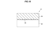
- FIG.10 is a cross sectional view showing a crystal layered structure in the fourth embodiment.
- a crystal layered structure 31 includes a Ga 2 O 3 substrate 32, a buffer layer 33 on the Ga 2 O 3 substrate 32 and a nitride semiconductor layer 34 on the buffer layer 33.
- the Ga 2 O 3 substrate 32 is formed of a ⁇ -Ga 2 O 3 single crystal.
- the principal surface of the Ga 2 O 3 substrate 32 is preferably a surface having oxygen atoms arranged in a hexagonal lattice pattern, e.g., a ( 101 ) plane, a (- 201 ) plane, a ( 301 ) plane or a ( 3-10 ) plane.
- a ( 101 ) plane is e.g., not more than 10 nm
- ( 101 ) is particularly preferable as the principal surface of the Ga 2 O 3 substrate 32.
- a percentage of the surface of the Ga 2 O 3 substrate 32 covered with the buffer layer 33 in a region immediately below the nitride semiconductor layer 4 is preferably from 10% to 90% in order to reduce electrical resistance between the Ga 2 O 3 substrate 32 and the nitride semiconductor layer 34, and the buffer layer 33 is formed in, e.g., an island pattern as shown in FIG.10 .
- the buffer layer 33 is formed of an AIN crystal, adhesion between the Ga 2 O 3 substrate 32 and the nitride semiconductor layer 34 is further increased.
- the thickness of the buffer layer 33 is, e.g., 5 nm.
- the thickness of the nitride semiconductor layer 34 is, e.g., 2 ⁇ m.
- the Ga 2 O 3 substrate 32 and the nitride semiconductor layer 34 may contain a conductive impurity such as Si.
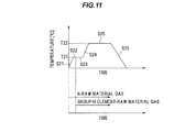
- FIG.11 is a graph showing an example manufacturing process sequence of the crystal layered structure in the present embodiment.
- FIG.12 is a graph showing an example manufacturing process sequence of a crystal layered structure in Comparative Example. Polygonal lines on the upper side of the graphs in FIG.11 and FIG.12 indicate variation in temperature condition over time, and arrows on the lower side of the graphs in FIG.11 and FIG.12 indicate time to supply the raw material gases.
- nitriding treatment of the surface of the Ga 2 O 3 substrate 32 is not performed before forming the buffer layer 33.
- the Ga 2 O 3 substrate 32 is subjected to pretreatment for 120 minutes using phosphoric acid of 98 wt% concentration heated to 150°C.
- the Ga 2 O 3 substrate 32 is delivered to a chamber of a MOCVD (Metal Organic Chemical Vapor Deposition) system and temperature in the chamber is then increased to T 21 while supplying an N-raw material gas such as N 2 or NH 3 to the chamber (Step S 21 ).
- T 21 is from 370 to 500°C, e.g., 450°C.
- the surface of the Ga 2 O 3 substrate 32 is exposed to the N-raw material gas for not more than 10 minutes, e.g., for 2 minutes while keeping the temperature in the chamber at T 21 (Step S 22 ).
- the temperature of the Ga 2 O 3 substrate 32 is stabilized by performing Step S 22 .
- the exposure time of the surface of the Ga 2 O 3 substrate 32 to the N-raw material gas, i.e., time to perform Step S 22 is more than 10 minutes, electrical resistance on the surface of the Ga 2 O 3 substrate 32 may increase due to excessive nitriding.
- Group III element raw material gases i.e., a Ga raw material gas such as trimethylgallium (TMG) gas, an Al raw material gas such as trimethyl aluminum (TMA) gas and an In raw material such as trimethylindium (TMI) gas are further fed to the chamber while keeping the temperature in the chamber at T 21 to grow an Al x Ga y In z N crystal on the Ga 2 O 3 substrate 32, thereby forming the buffer layer 33 (Step S 23 ).
- TMG trimethylgallium
- TMA trimethyl aluminum
- TMI trimethylindium
- T 22 is, e.g., 1050°C.
- Step S 25 an Al x Ga y In z N crystal is grown on the buffer layer 33 while keeping the temperature in the chamber at T 22 , thereby forming the nitride semiconductor layer 34 (Step S 25 ).
- Step S 26 the temperature in the chamber is reduced (Step S 26 ) and the crystal layered structure 31 is taken out from the chamber.
- the Ga 2 O 3 substrate 32 is subjected to pretreatment for 120 minutes using phosphoric acid of 98 wt% concentration heated to 150°C.
- the Ga 2 O 3 substrate 32 is delivered to a chamber of a MOCVD (Metal Organic Chemical Vapor Deposition) system and temperature in the chamber is then increased to T 20 while supplying an N-raw material gas to the chamber (Step S 31 ).
- T 20 is higher than T 21 described above and is, e.g., 800°C.
- Step S 32 the temperature in the chamber is kept at T 20 and nitriding treatment is performed on the surface of the Ga 2 O 3 substrate 32 (Step S 32 ).
- T 21 here is the same temperature as T 21 shown in FIG.11 .
- group III element raw material gases are fed to the chamber while keeping the temperature in the chamber at T 21 to grow an Al x Ga y In z N crystal on the Ga 2 O 3 substrate 32, thereby forming the buffer layer 33 (Step S 34 ).
- Steps S 35 to 37 are the same as the previously mentioned Steps S 24 to 26 and the explanation thereof is omitted.
- the buffer layer is formed by growing an Al x Ga y In z N crystal on the Ga 2 O 3 substrate (Step S 23 ) after the Ga 2 O 3 substrate is kept for not more than 10 minutes in a state of being exposed to nitrogen raw material gas (Step S 22 ), which allows a high-quality nitride semiconductor layer to be formed without performing nitriding treatment on the Ga 2 O 3 substrate (nitriding treatment at higher temperature than the growth temperature of the Al x Ga y In z N crystal of the buffer layer) before forming the buffer layer.
- nitriding treatment is not performed, a nitrided portion having high electrical resistance is hardly formed on the surface of the Ga 2 O 3 substrate and it is thus possible to obtain a crystal layered structure in which electrical resistance between the Ga 2 O 3 substrate and the nitride semiconductor layer is low. In addition, it is possible to obtain a low-voltage driving semiconductor element by using such a crystal layered structure.
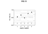
- a predetermined magnitude of current was passed between the Ga 2 O 3 substrate 32 and the nitride semiconductor layer 34 of the crystal layered structure 31 in the fourth embodiment and voltage was measured.
- an AIN layer formed of an AIN crystal was used as the buffer layer 33 and a GaN layer formed of a GaN crystal was used as the nitride semiconductor layer 34.
- first crystal layered structure Five crystal layered structures 31, which were made through a process in which Step S 22 in FIG. 11 was performed for 2 minutes (within the limit defined in the fourth embodiment)
- second crystal layered structure Five crystal layered structures 31, which were made through a process in which Step S 22 was performed for 30 minutes (out of the limit defined in the fourth embodiment)
- FIG.13 shows measured values of voltage between the Ga 2 O 3 substrate and the nitride semiconductor layer when a current of a predetermined magnitude flows through a crystal layered structure.
- the horizontal axis indicates the sample number of the crystal layered structure and the vertical axis indicates voltage [V] between the Ga 2 O 3 substrate and the nitride semiconductor layer when a current flows through the surface of the nitride semiconductor layer at a current density of 200 A/cm 2 .
- open diamonds indicate values measured on the first crystal layered structures and filled diamonds indicate values measured on the second crystal layered structures. Electrodes were respectively connected to the Ga 2 O 3 substrate and the GaN crystal layer and voltage was then measured.
- a crystal layered structure having a low dislocation density on the upper surface of a nitride semiconductor layer on a Ga 2 O 3 substrate and a method for manufacturing the crystal layered structure.
- a crystal layered structure having low electrical resistance between the Ga 2 O 3 substrate and the nitride semiconductor layer a method for manufacturing the crystal layered structure and a semiconductor element including the crystal layered structure and driven at low voltage.
- a method for manufacturing a crystal layered structure having low electrical resistance between the Ga 2 O 3 substrate and the nitride semiconductor layer is provided.
Landscapes
- Chemical & Material Sciences (AREA)
- Engineering & Computer Science (AREA)
- Crystallography & Structural Chemistry (AREA)
- Materials Engineering (AREA)
- Metallurgy (AREA)
- Organic Chemistry (AREA)
- Chemical Kinetics & Catalysis (AREA)
- General Chemical & Material Sciences (AREA)
- Inorganic Chemistry (AREA)
- Led Devices (AREA)
- Recrystallisation Techniques (AREA)
Abstract
Description
- The invention relates to a crystal layered structure (or laminated crystal structure) and a method for manufacturing the crystal layered structure (or laminated crystal structure), and a semiconductor element.
- An LED element is known that includes a crystal layered structure composed of a Ga2O3 substrate, an AIN buffer layer and a GaN layer (see e.g. PTL 1). In
PTL 1, the GaN layer is formed by growing a GaN crystal on the AIN buffer layer under the temperature condition of 1050°C. - In addition, in
PTL 1, the AIN buffer layer is formed on the Ga2O3 substrate so as to completely cover the upper surface of the Ga2O3 substrate, and the GaN layer is formed on the AIN buffer layer. The crystal quality of the GaN layer can be improved by forming the AIN buffer layer. - Also, the manufacturing process of the semiconductor element disclosed in
PTL 1 is conducted such that a surface of the Ga2O3 substrate is subjected to a nitriding treatment before forming the AIN buffer layer to grow the GaN crystal on the Ga2O3 substrate. - [PTL 1]
JP-A-2006-310765 - However, in the method disclosed in
PTL 1, the oxygen concentration in the GaN layer decreases since the GaN crystal is grown under the high temperature condition of 1050°C. Therefore, the dislocation density on the upper surface of the GaN layer (a surface opposite to the AIN buffer layer) increases and this causes a leakage current to occur in a low voltage region when voltage is applied in the vertical direction to the element which includes the crystal layered structure. - Also, there is a problem that the semiconductor element disclosed in
PTL 1 does not operate at a low voltage due to the high electrical resistance between the Ga2O3 substrate and the GaN layer on the AIN buffer layer. - Also, since the electrical resistance increases at the nitrided portion of the Ga2O3 substrate, the semiconductor element disclosed in
PTL 1 has a high electrical resistance between the Ga2O3 substrate and the nitride semiconductor layer and does not operate at a low voltage. - It is an object of the invention to provide a crystal layered structure that has a low dislocation density on the upper surface of a nitride semiconductor layer on a Ga2O3 substrate, as well as a method for manufacturing the crystal layered structure.
- It is another object of the invention to provide a crystal layered structure that has a low electrical resistance between the Ga2O3 substrate and the nitride semiconductor layer, as well as a method for manufacturing the crystal layered structure and a semiconductor element including the crystal layered structure and driven at low voltage.
- It is another object of the invention to provide a method for manufacturing a crystal layered structure that has a low electrical resistance between the 00269Ga2O3 substrate and the nitride semiconductor layer.
- According to one embodiment of the invention, a crystal layered structure as defined in [1] to [6] below and a method for manufacturing a crystal layered structure as defined in [7] to [10] below are provided so as to achieve one of the above objects.
- [1] A crystal layered structure, comprising:
- a Ga2O3 substrate;
- a buffer layer comprising an AlxGayInzN (0≤x≤1, 0≤y≤1, 0≤z≤1, x+y+z=1) crystal on the Ga2O3 substrate; and
- a nitride semiconductor layer comprising an AlxGayInzN (0≤x≤1, 0≤y≤1, 0≤z≤1, x+y+z=1) crystal containing oxygen as an impurity on the buffer layer,
- wherein an oxygen concentration in a region on a side of the Ga2O3 substrate of the nitride semiconductor layer, region having a thickness of not less than 200 nm, is not less than 1.0x10¹⁸ /cm3.
- [2] The crystal layered structure according to [1], wherein the nitride semiconductor layer has a dislocation density of less than 1.0x10⁹ /cm2 on a surface thereof opposite the Ga2O3 substrate.
- [3] The crystal layered structure according to [1] or [2], wherein an oxygen concentration in a region on the side of the Ga2O3 substrate of the nitride semiconductor layer, the region having a thickness of not less than 500 nm, is not less than 1.0x10¹⁸ /cm3.
- [4] The crystal layered structure according to [1] or [2], wherein the oxygen concentration in the region is not less than 5.0x10¹⁸ /cm3.
- [5] The crystal layered structure according to [1] or [2], wherein the AlxGayInzN crystal of the buffer layer comprises an AIN crystal.
- [6] The crystal layered structure according to [1] or [2], wherein the AlxGayInzN crystal of the nitride semiconductor layer comprises a GaN crystal.
- [7] A method for manufacturing a crystal layered structure, comprising:
- a step of forming a buffer layer by growing a first AlxGayInzN (0≤x≤1, 0≤y≤1, 0≤z≤1, x+y+z=1) crystal on a Ga2O3 substrate; and
- a step of forming a nitride semiconductor layer by growing a second AlxGayInzN (0≤x≤1, 0≤y≤1, 0≤z≤1, x+y+z=1) crystal on the buffer layer,
- wherein the second AlxGayInzN crystal is initially grown at a first temperature of not more than 1000°C and is then grown at a second temperature higher than the first temperature in the step of forming the nitride semiconductor layer, and
- wherein the second AlxGayInzN crystal grown at the first temperature is not less than 200 nm in thickness.
- [8] The method for manufacturing a crystal layered structure according to [7], wherein the second AlxGayInzN crystal grown at the first temperature is not less than 500 nm in thickness.
- [9] The method for manufacturing a crystal layered structure according to [7] or [8], wherein the first AlxGayInzN crystal comprises an AIN crystal.
- [10] The method for manufacturing a crystal layered structure according to [7] or [8], wherein the second AlxGayInzN crystal comprises a GaN crystal.
According to one embodiment of the invention, a crystal layered structure as defined in [11] to [16] below, a semiconductor element as defined in [17] and a method for manufacturing a crystal layered structure as defined in [18] to [23] below are provided so as to achieve one of the above objects. - [11] A crystal layered structure, comprising:
- a Ga2O3 substrate;
- a buffer layer comprising an AlxGayInzN (0≤x≤1, 0≤y≤1, 0≤z≤1, x+y+z=1) crystal on the Ga2O3 substrate; and
- a nitride semiconductor layer comprising an AlxGayInzN (0≤x≤1, 0≤y≤1, 0≤z<1, x+y+z=1) crystal on the buffer layer,
- wherein a percentage of a surface of the Ga2O3 substrate covered with the buffer layer in a region immediately below the nitride semiconductor layer is not less than 10% and less than 100%, and
- wherein a portion of the nitride semiconductor layer is in contact with the surface of the Ga2O3 substrate.
- [12] The crystal layered structure according to [11], wherein the percentage is not more than 90%.
- [13] The crystal layered structure according to [11] or [12], wherein the buffer layer comprises the AlxGayInzN crystal arranged in an island pattern on the Ga2O3 substrate.
- [14] The crystal layered structure according to [11] or [12], wherein the buffer layer comprises the AlxGayInzN crystal in a film shape comprising a hole.
- [15] The crystal layered structure according to [11] or [12], wherein the AlxGayInzN crystal of the buffer layer comprises an AIN crystal.
- [16] The crystal layered structure according to [11] or [12], wherein the AlxGayInzN crystal of the nitride semiconductor layer comprises a GaN crystal.
- [17] A semiconductor element, comprising:
- the crystal layered structure according to [11] or [12],
- wherein the Ga2O3 substrate and the nitride semiconductor layer are configured to allow electrical conduction therethrough.
- [18] A method for manufacturing a crystal layered structure, comprising:
- a step of forming a buffer layer by growing a first AlxGayInzN (0≤x≤1, 0≤y≤1, 0≤z≤1, x+y+z=1) crystal on a Ga2O3 substrate so as to partially cover a surface of the Ga2O3 substrate; and
- a step of forming a nitride semiconductor layer by growing a second AlxGayInzN (0≤x≤1, 0≤y≤1, 0≤z≤1, x+y+z=1) crystal on the buffer layer,
- wherein a percentage of a surface of the Ga2O3 substrate covered with the buffer layer in a region immediately below the nitride semiconductor layer is not less than 10% and less than 100%, and
- wherein a portion of the nitride semiconductor layer is in contact with the surface of the Ga2O3 substrate.
- [19] The method for manufacturing a crystal layered structure according to [18], wherein the percentage is not more than 90%.
- [20] The method for manufacturing a crystal layered structure according to [18] or [19], wherein the buffer layer is formed by growing the first AlxGayInzN crystal in an island pattern on the Ga2O3 substrate.
- [21] The method for manufacturing a crystal layered structure according to [18] or [19], wherein the buffer layer is formed by growing the first AlxGayInzN crystal in a film shape comprising a hole on the Ga2O3 substrate.
- [22] The method for manufacturing a crystal layered structure according to [18] or [19], wherein the first AlxGayInzN crystal comprises an AIN crystal.
- [23] The method for manufacturing a crystal layered structure according to [18] or [19], wherein the second AlxGayInzN crystal comprises a GaN crystal.
According to one embodiment of the invention, a method for manufacturing a crystal layered structure as defined in [24] to [28] below is provided so as to achieve one of the above objects. - [24] A method for manufacturing a crystal layered structure, comprising:
- a step of forming a buffer layer by growing a first AlxGayInzN (0≤x≤1, 0≤y≤1, 0≤z≤1, x+y+z=1) crystal at a first temperature on a Ga2O3 substrate of which principal surface is a surface having an oxygen atom arranged in a hexagonal lattice pattern; and
- a step of forming a nitride semiconductor layer by growing a second AlxGayInzN (0≤x≤1, 0≤y≤1, 0≤z≤1, x+y+z=1) crystal on the buffer layer,
- wherein a step of nitriding a surface of the Ga2O3 substrate at a higher temperature than the first temperature is not performed before forming the buffer layer.
- [25] The method for manufacturing a crystal layered structure according to [24], wherein the Ga2O3 substrate is kept at the first temperature for not more than 10 minutes in a state of being exposed to a nitrogen raw material gas and is then kept at the first temperature in a state of being exposed to the N-raw material gas and an A1 raw material gas to grow the second AlxGayInzN crystal.
- [26] The method for manufacturing a crystal layered structure according to [24] or [25], wherein the principal surface of the Ga2O3 substrate comprises one of (101), (-201), (301) and (3-10) planes.
- [27] The method for manufacturing a crystal layered structure according to [24] or [25], wherein the first AlxGayInzN crystal comprises an AIN crystal.
- [28] The method for manufacturing a crystal layered structure according to [24] or [25], wherein the second AlxGayInzN crystal comprises a GaN crystal.
- According to one embodiment of the invention, a crystal layered structure can be provided that has a low dislocation density on the upper surface of a nitride semiconductor layer on a Ga2O3 substrate, as well as a method for manufacturing the crystal layered structure.
- According to one embodiment of the invention, a crystal layered structure can be provided that has a low electrical resistance between the Ga2O3 substrate and the nitride semiconductor layer, as well as a method for manufacturing the crystal layered structure and a semiconductor element including the crystal layered structure and driven at low voltage.
- According to one embodiment of the invention, a method for manufacturing a crystal layered structure can be provided that has a low electrical resistance between the Ga2O3 substrate and the nitride semiconductor layer.
-
- [
FIG.1 ]
FIG.1 is a cross sectional view showing a crystal layered structure in a first embodiment. - [
FIG.2 ]
FIG.2 is a graph showing an example manufacturing process sequence of the crystal layered structure in the first embodiment. - [
FIG.3 ]
FIG.3 is a graph of Example 1 showing a relation between a thickness of a high oxygen concentration layer and dislocation density on an upper surface of a nitride semiconductor layer and a relation between an oxygen concentration in the high oxygen concentration layer and the dislocation density on the upper surface of the nitride semiconductor layer. - [
FIG.4 ]
FIG.4 is a cross sectional view showing an LED element in Example 2. - [
FIG.5 ]
FIGS is a cross sectional view showing a crystal layered structure in a second embodiment. - [
FIG.6 ]
FIG.6 is a cross sectional view showing an LED element in a third embodiment. - [
FIG.7A ]
FIG7A is a SEM image of a buffer layer in Example 3. - [
FIG.7B ]
FIG.7B is a SEM image of a buffer layer in Example 3. - [
FIG.8 ]
FIG.8 is a graph of Example 3 showing a relation between the supply quantity of Al raw material to a chamber of a MOCVD system and the coverage rate of an AIN crystal layer as the buffer layer. - [
FIG.9 ]
FIG.9 is a graph of Example 3 showing a relation between the coverage rate of an AIN crystal layer as the buffer layer and voltage between a Ga2O3 substrate and a GaN crystal layer as a nitride semiconductor layer when a current of a predetermined magnitude flows. - [
FIG.10 ]
FIG.10 is a cross sectional view showing a crystal layered structure in a fourth embodiment. - [
FIG.11 ]
FIG.11 is a graph showing an example manufacturing process sequence of the crystal layered structure in the fourth embodiment. - [
FIG.12 ]
FIG.12 is a graph showing an example manufacturing process sequence of a crystal layered structure in Comparative Example. - [
FIG.13 ]
FIG.13 shows measured values of voltage between the Ga2O3 substrate and the nitride semiconductor layer when a current of a predetermined magnitude flows through a crystal layered structure in Example 5. -
FIG.1 is a cross sectional view showing a crystal layeredstructure 11 in the first embodiment. The crystal layeredstructure 11 includes a Ga2O3 substrate 12, abuffer layer 13 on the Ga2O3 substrate 12 and anitride semiconductor layer 14 on thebuffer layer 13. - The Ga2O3 substrate 12 is formed of a β-Ga2O3 single crystal.
- The
buffer layer 13 is formed of an AlxGayInzN (0≤x≤1, 0≤y≤1, 0≤z≤1, x+y+z=1) crystal. In addition, the coverage rate of thebuffer layer 13 on the upper surface of the Ga2O3 substrate 12 is preferably 10 to 90% in order to successfully form a highoxygen concentration layer 14a of thenitride semiconductor layer 14 described later, and thebuffer layer 13 is formed in, e.g., an island pattern as shown inFIG.1 . - In addition, among the AlxGayInzN crystals, an AIN crystal (x=1, y=z=0) is especially preferable to form the
buffer layer 13. When thebuffer layer 13 is formed of an AIN crystal, adhesion between the Ga2O3 substrate 12 and thenitride semiconductor layer 14 is further increased. - The
nitride semiconductor layer 14 includes a highoxygen concentration layer 14a in contact with thebuffer layer 13 and a lowoxygen concentration layer 14b on the highoxygen concentration layer 14a. The nitride semiconductor layer 14 (the highoxygen concentration layer 14a and the lowoxygen concentration layer 14b) is formed of an AlxGayInzN (0≤x≤1, 0≤y≤1, 0≤z≤1, x+y+z=1) crystal containing oxygen as an impurity and is preferably formed of especially a GaN crystal (y=1, x=z=0) having good crystal quality. The thickness of thenitride semiconductor layer 14 is, e.g., 3 µm. - On the upper surface of the nitride semiconductor layer 14 (a surface opposite to the Ga2O3 substrate 12), i.e., on the upper surface of the low
oxygen concentration layer 14b, dislocation density is low and occurrence of leakage current in a low voltage region is thus suppressed when voltage is applied in the vertical direction to an element including the crystal layeredstructure 11. The leakage current can be suppressed to a practicable level especially when the dislocation density on the upper surface of the lowoxygen concentration layer 14b is less than 1.0x10⁹ /cm2. - The oxygen concentration in the high
oxygen concentration layer 14a is higher than that in the lowoxygen concentration layer 14b and is not less than 1.0x10¹⁸ /cm3. In addition, the thickness of the highoxygen concentration layer 14a is not less than 200 nm. The dislocation density on the upper surface of thenitride semiconductor layer 14 is reduced by providing the highoxygen concentration layer 14a. - In addition, in order to further reduce the dislocation density on the upper surface of the
nitride semiconductor layer 14, the oxygen concentration in the highoxygen concentration layer 14a is preferably not less than 5.0x10¹⁸/cm3 and the thickness of the highoxygen concentration layer 14a is preferably not less than 500 nm. - It should be noted that in order to prevent pits (holes) from being formed on a surface of the
nitride semiconductor layer 14, a semiconductor crystal to be finally formed needs to be grown at high temperature and the lowoxygen concentration layer 14b having a relatively low oxygen concentration is thus formed. - The Ga2O3 substrate 12 and the nitride semiconductor layer 14 (the high
oxygen concentration layer 14a and the lowoxygen concentration layer 14b) may contain a conductive impurity such as Si. -
FIG.2 is a graph showing an example manufacturing process of the crystal layered structure in the present embodiment. A polygonal line inFIG.2 indicates variation in temperature condition over time. - Firstly, the Ga2O3 substrate 12 is subjected to pretreatment for 120 minutes using phosphoric acid of 98 wt% concentration heated to 150°C. A surface of the Ga2O3 substrate 12 is etched about 1000 nm in the pretreatment.
- Next, the Ga2O3 substrate 12 is delivered to a chamber of a MOCVD (Metal Organic Chemical Vapor Deposition) system and temperature in the chamber is then increased to T11 (Step S11). Here, T11 is from 350 to 600°C, e.g., 450°C.
- Next, NH3 gas as an N raw material, trimethylgallium (TMG) as a Ga raw material, trimethyl aluminum (TMA) as an Al raw material and trimethylindium (TMI) as an In raw material are fed to the chamber while keeping the temperature in the chamber at T11 to grow an AlxGayInzN crystal on the Ga2O3 substrate 12, thereby forming the buffer layer 13 (Step S12).
- Next, the temperature in the chamber is increased to T12 (Step S13). Here, T12 is not more than 1000°C, e.g., 950°C. If T12 is more than 1000°C, the oxygen concentration in the high
oxygen concentration layer 14a is highly likely to decrease. - Next, NH3, TMG, TMA and TMI are fed to the chamber while keeping the temperature in the chamber at T12 to grow an AlxGayInzN crystal on the
buffer layer 13, thereby forming the highoxygen concentration layer 14a of the nitride semiconductor layer 14 (Step S14). - Next, the temperature in the chamber is increased to T13 while continuously feeding each raw material gas (Step S15). Here, T13 is higher than T12 and is preferably higher than 1000°C, e.g., 1050°C.
- Next, the AlxGayInzN crystal is continuously grown while keeping the temperature in the chamber at T13, thereby forming the low
oxygen concentration layer 14b of the nitride semiconductor layer 14 (Step S16). As a result, the crystal layeredstructure 11 is obtained. - After that, the temperature in the chamber is reduced (Step S17) and the crystal layered
structure 11 is taken out from the chamber. - In the first embodiment, by providing a high oxygen concentration region in the nitride semiconductor layer on the Ga2O3 substrate side, it is possible to form a crystal layered structure in which dislocation density on the upper surface of the nitride semiconductor layer is low. Therefore, occurrence of leakage current in a low voltage region can be suppressed in case that an element such as LED element is formed using such a crystal layered structure.
- In Example 1, a relation between the thickness of the high
oxygen concentration layer 14a and the dislocation density on the upper surface of thenitride semiconductor layer 14 and a relation between the oxygen concentration in the highoxygen concentration layer 14a and the dislocation density on the upper surface of thenitride semiconductor layer 14 in the crystal layeredstructure 11 in the first embodiment were evaluated. - Twelve crystal layered structures, in which respective high oxygen concentration layers corresponding to the high
oxygen concentration layer 14a have different oxygen concentrations and thicknesses, were prepared and evaluated. Here, each high oxygen concentration layer has the oxygen concentration of 1.0x10¹⁷ /cm 3 , 1.0x10¹⁸ /cm 3 or 5.0x10¹⁸ /cm 3 and the thickness of 100 nm, 200 nm, 500 nm or 1000 nm. Of those, the high oxygen concentration layers having the oxygen concentration of not less than 1.0x10¹⁸ /cm 3 as well as the thickness of not less than 200 nm correspond to the highoxygen concentration layer 14a in the first embodiment of the invention. - It should be noted that the high oxygen concentration layers having the oxygen concentration of 1.0x10¹⁷ /cm 3 , 1.0x10¹⁸ /cm 3 and 5.0x10¹⁸ /cm 3 were respectively formed under the temperature condition of T12=1050°C, 1000°C and 950°C.
- It should be noted that in any of the crystal layered structures in the present Example, the buffer layer corresponding to the
buffer layer 13 was a 5 nm-thick AIN crystal film formed under the temperature condition of T11=450°C, the low oxygen concentration layer corresponding to the lowoxygen concentration layer 14b and the high oxygen concentration layer were GaN crystal films containing Si, the nitride semiconductor layer corresponding to thenitride semiconductor layer 14 had a thickness (the total of the thickness of the high oxygen concentration layer and the thickness of the low oxygen concentration layer) of 3 µm, and the low oxygen concentration layer was formed under the temperature condition of T13=1050°C. -
FIG.3 is a graph of Example 1 showing a relation between a thickness of the high oxygen concentration layer and dislocation density on the upper surface of the nitride semiconductor layer and a relation between an oxygen concentration in the high oxygen concentration layer and the dislocation density on the upper surface of the nitride semiconductor layer. InFIG.3 , the vertical axis indicates dislocation density [/cm] on the upper surface of the nitride semiconductor layer and the horizontal axis indicates a thickness [nm] of the high oxygen concentration layer. - In
FIG.3 , open circles indicate values measured on the crystal layered structures with a high oxygen concentration layer having the oxygen concentration of 1.0x10¹⁷ /cm 3 , open diamonds indicate values measured on the crystal layered structures with a high oxygen concentration layer having the oxygen concentration of 1.0x10¹⁸ /cm 3 and filled diamonds indicate values measured on the crystal layered structures with a high oxygen concentration layer having the oxygen concentration of 5.0x10¹⁸ /cm 3 . - As shown in
FIG.3 , the higher the oxygen concentration in the high oxygen concentration layer, the lower the dislocation density on the upper surface of the nitride semiconductor layer. In addition, the thicker the high oxygen concentration layer, the lower the dislocation density on the upper surface of the nitride semiconductor layer. Especially when the high oxygen concentration layer has the oxygen concentration of not less than 1.0x10¹⁸ /cm 3 and the thickness of not less than 200 nm, i.e., when the high oxygen concentration layer corresponds to the highoxygen concentration layer 14a, the dislocation density on the upper surface of the nitride semiconductor layer is less than 1.0x10⁹ /cm 2 and it is possible to effectively suppress leakage current which occurs in a low voltage region when voltage is applied in the vertical direction to an element including such a crystal layered structure. - In Example 2, voltage was applied in the vertical direction to an LED element formed using the crystal layered
structure 11 in the first embodiment and a level of leakage current in a low voltage region was evaluated. -
FIG.4 is a cross sectional view showing an LED element formed using the crystal layered structure in the first embodiment. AnLED element 100 has a Ga2O3 substrate 112, abuffer layer 113 on the Ga2O3 substrate 112, an n-GaN layer 114 on thebuffer layer 113, a light-emittinglayer 115 on the n-GaN layer 114, a p-GaN layer 116 on the light-emittinglayer 115, acontact layer 117 on the p-GaN layer 116, a p-type electrode 118 on thecontact layer 117 and an n-type electrode 119 on a surface of the Ga2O3 substrate 112 opposite to thebuffer layer 113. - The
LED element 100 is a light-emitting element of which light extraction surface is located on the Ga2O3 substrate 112 side. A laminated body composed of the n-GaN layer 114, the light-emittinglayer 115, the p-GaN layer 116 and thecontact layer 117 has a mesa shape of which side surfaces are covered with an SiO2 film 120. - Here, the Ga2O3 substrate 112, the
buffer layer 113 and thenitride semiconductor layer 114 correspond to the Ga2O3 substrate 12, thebuffer layer 13 and the n-GaN layer 14 in the first embodiment, and the laminated body composed of the Ga2O3 substrate 12, thebuffer layer 113 and the n-GaN layer 114 corresponds to the crystal layeredstructure 11 in the first embodiment. - The n-
GaN layer 114 includes a highoxygen concentration layer 114a and a lowoxygen concentration layer 114b. The highoxygen concentration layer 114a and the lowoxygen concentration layer 114b respectively correspond to the highoxygen concentration layer 14a and the lowoxygen concentration layer 14b in the first embodiment. - The Ga2O3 substrate 112 is an n-type β-Ga2O3 substrate containing Si. In addition, the Ga2O3 substrate 112 is 400 µm in thickness and has a principal surface oriented in (101).
- The
buffer layer 113 is a 5 nm-thick AIN crystal film formed at a growth temperature of 450°C. - The high
oxygen concentration layer 114a is an n-type GaN crystal film which contains Si and is formed at a growth temperature of 950°C. The highoxygen concentration layer 114a includes a 10 nm-thick lower region having a Si concentration of 2.0x10¹⁹ /cm 3 and a 1000 nm-thick upper region having a Si concentration of 5.0x10¹⁸ /cm 3 . It should be noted that monomethylsilane gas is used as an Si raw material. - The low
oxygen concentration layer 114b is a 3 µm-thick n-type GaN crystal film formed at a growth temperature of 1050°C. The lowoxygen concentration layer 114b contains Si at a concentration of 1.0x10¹⁸ /cm 3 . - The light-emitting
layer 115 is composed of three layers of multiple quantum well structures formed at a growth temperature of 750°C and a 10 nm-thick GaN crystal film thereon. Each multiple quantum well structure is composed of an 8 nm-thick GaN crystal film and a 2 nm-thick InGaN crystal film. - The p-
GaN layer 116 is a 150 nm-thick p-type GaN crystal film formed at a growth temperature of 1000°C. The p-GaN layer 116 contains Mg at a concentration of 5.0x10¹⁹ /cm 3 . It should be noted that cyclopentadienyl magnesium gas is used as an Mg raw material. - The
contact layer 117 is a 10 nm-thick p-type GaN crystal film formed at a growth temperature of 1000°C. Thecontact layer 117 contains Mg at a concentration of 1.5x10²⁰ /cm 3 . - Meanwhile, an LED element in which a 3 µm-thick n-type GaN crystal film formed at a growth temperature of 1050°C is used in place of the high
oxygen concentration layer 114a was prepared as Comparative Example. This GaN crystal film contains Si at the same concentration as in the highoxygen concentration layer 114a of theLED element 100. - The
LED element 100 and the LED in Comparative Example were respectively mounted on can-type stems using Ag paste, and current values when voltage of 2.0V was applied between electrodes were measured. - As a result, the current value of the
LED element 100 was 0.35 µA while the current value of the LED in Comparative Example was 20 µA. It was confirmed from this result that occurrence of leakage current in a low voltage region is suppressed in theLED element 100. -
FIG.5 is a cross sectional view showing a crystal layered structure in the second embodiment. A crystal layeredstructure 21 includes a Ga2O3 substrate 22, abuffer layer 23 on the Ga2O3 substrate 22 and anitride semiconductor layer 24 on thebuffer layer 23. - The Ga2O3 substrate 22 is formed of a β-Ga2O3 single crystal.
- ] The
buffer layer 23 is formed of an AlxGayInzN (0≤x≤1, 0≤y≤1, 0≤z≤1, x+y+z=1) crystal. A percentage of the surface of the Ga2O3 substrate 22 covered with thebuffer layer 23 in a region immediately below the nitride semiconductor layer 24 (hereinafter, also referred as "coverage rate of thebuffer layer 23") is not less than 10% and less than 100%, and preferably, not less than 10% and not more than 90%. When the coverage rate is, e.g., 10%, the shape of thebuffer layer 23 is an island pattern as shown inFIG.5 . Meanwhile, when the coverage rate is 90%, thebuffer layer 23 has a film shape with holes. - When the coverage rate of the
buffer layer 23 is less than 100%, thenitride semiconductor layer 24 is directly in contact with the surface of the Ga2O3 substrate 22 in a region not covered with thebuffer layer 23 and electrical resistance between the Ga2O3 substrate 22 and thenitride semiconductor layer 24 is reduced. Electrical resistance between the Ga2O3 substrate 22 and thenitride semiconductor layer 24 drops especially when the coverage rate is not more than 90%. - On the other hand, when the coverage rate is lower than 10%, the
buffer layer 23 does not serve as a buffer layer when forming thenitride semiconductor layer 24, which causes a decrease in crystal quality of thenitride semiconductor layer 24 and an increase in electrical resistance. - Among the AlxGayInzN crystals, an AIN crystal (x=1, y=z=0) is especially preferable to form the
buffer layer 23. When thebuffer layer 23 is formed of an AIN crystal, adhesion between the Ga2O3 substrate 22 and thenitride semiconductor layer 24 is further increased. - The
nitride semiconductor layer 24 is formed of an AlxGayInzN (0≤x≤1, 0≤y≤1, 0≤z≤1, x+y+z=1) crystal and is preferably formed of especially a GaN crystal (y=1, x=z=0) having good crystal quality. The thickness of thenitride semiconductor layer 24 is, e.g., 5 µm. - It should be noted that the Ga2O3 substrate 22 and the
nitride semiconductor layer 24 may contain a conductive impurity such as Si. - An example manufacturing process of the crystal layered structure in the present embodiment will be described below.
- Firstly, the Ga2O3 substrate 22 is subjected to pretreatment for 120 minutes. A surface of the Ga2O3 substrate 22 is etched about 1000 nm in the pretreatment.
- Next, the Ga2O3 substrate 22 is delivered to a chamber of a MOCVD (Metal Organic Chemical Vapor Deposition) system.
- Next, NH3 gas as an N raw material, trimethylgallium (TMG) gas as a Ga raw material, trimethyl aluminum (TMA) gas as an Al raw material and trimethylindium (TMI) gas as an In raw material are fed to the chamber while keeping the temperature in the chamber at 370 to 500°C to grow an AlxGayInzN crystal on the Ga2O3 substrate 22, thereby forming the
buffer layer 23. At this stage, thebuffer layer 23 is a film having uniform thickness and covers 100% of the surface of the Ga2O3 substrate 22. It should be noted that raw materials of the respective elements are not limited to the above. - Next, the temperature in the chamber is increased to, e.g., 1000°C. Here, the
buffer layer 23 undergoes a change on the Ga2O3 substrate 22 and is transformed into an island pattern or a perforated film once the temperature in the chamber reaches a predetermined temperature, e.g., 800°C. As a result, a percentage of the surface of the Ga2O3 substrate 22 covered with thebuffer layer 23 becomes not less than 10% and less than 100%. - In this regard, however, the larger the supply quantities of raw materials of the group III elements (Al, Ga, In) and the group V element (N)at the time of forming the
buffer layer 23, the higher the coverage rate of thebuffer layer 23 after transformation. Therefore, the supply quantities of such raw materials need to be controlled so that the coverage rate is not 100%. - Next, NH3 gas, TMG gas, TMA gas and TMI gas are fed to the chamber while keeping the temperature in the chamber at, e.g., 1000°C to grow an AlxGayInzN crystal on the
buffer layer 23, thereby forming thenitride semiconductor layer 24. As a result, the crystal layeredstructure 21 is obtained. - The third embodiment is a semiconductor element including the crystal layered
structure 21 in the first embodiment. An LED element will be described below as an example of such a semiconductor element. -
FIG.6 is a cross sectional view showing an LED element in the third embodiment. AnLED element 200 has a Ga2O3 substrate 212, abuffer layer 213 on the Ga2O3 substrate 212, anitride semiconductor layer 214 on thebuffer layer 213, a light-emittinglayer 215 on thenitride semiconductor layer 214, a p-GaN layer 216 on the light-emittinglayer 215, acontact layer 217 on the p-GaN layer 216, a p-type electrode 218 on thecontact layer 217 and an n-type electrode 219 on a surface of the Ga2O3 substrate 212 opposite to thebuffer layer 213. - The
LED element 200 is a light-emitting element of which light extraction surface is located on the Ga2O3 substrate 212 side. A laminated body composed of thenitride semiconductor layer 214, the light-emittinglayer 215, the p-GaN layer 216 and thecontact layer 217 has a mesa shape of which side surfaces are covered with an SiO2 film 220. - Here, the Ga2O3 substrate 212, the
buffer layer 213 and thenitride semiconductor layer 214 correspond to the Ga2O3 substrate 22, thebuffer layer 23 and thenitride semiconductor layer 24 in the second embodiment, and the laminated body composed of the Ga2O3 substrate 212, thebuffer layer 213 and thenitride semiconductor layer 214 corresponds to the crystal layeredstructure 21 in the second embodiment. - The
LED element 200 is a vertical-type semiconductor element in which electricity is conducted to the Ga2O3 substrate 212 and thenitride semiconductor layer 24 during operation. The Ga2O3 substrate 212 and thenitride semiconductor layer 214 are directly in contact with each other and electrical resistance therebetween is low. Therefore, theLED element 200 can operate at low voltage. - The Ga2O3 substrate 212 is an n-type β-Ga2O3 substrate. The Ga2O3 substrate 212 is, e.g., 400 µm in thickness and has a principal surface oriented in (101).
- The
buffer layer 213 is, e.g., a 5 nm-thick n-type AlxGayInzN crystal film. - The
nitride semiconductor layer 214 is, e.g., a 5 µm-thick n-type AlxGayInzN crystal film. - The light-emitting
layer 215 is composed of, e.g., three layers of multiple quantum well structures and a 10 nm-thick GaN crystal film thereon. Each multiple quantum well structure is composed of an 8 nm-thick GaN crystal film and a 2 nm-thick InGaN crystal film. - The p-
GaN layer 216 is, e.g., a 150 nm-thick p-type GaN crystal film. - In the second and third embodiments, the percentage of the surface of the Ga2O3 substrate covered with the buffer layer in a region immediately below the nitride semiconductor layer (the coverage rate of the buffer layer) is controlled and it is thereby possible to obtain a crystal layered structure in which electrical resistance between the Ga2O3 substrate and the nitride semiconductor layer is low. In addition, it is possible to obtain a low-voltage driving semiconductor element by using such a crystal layered structure.
-
FIG7A and FIG.7B are SEM (Scanning Electron Microscope) images of buffer layers in Example 3.FIG.7A and FIG.7B show AIN crystal layers as thebuffer layer 23 each grown on the Ga2O3 substrate 22 at a growth temperature of 450°C and then heated to 1050°C. - The AIN crystal layer shown in
FIG.7A is formed of plural AIN crystals which are formed in an island pattern on the Ga2O3 substrate 22, and the coverage rate thereof is about 35%. - The AIN crystal layer shown in
FIG.7B is formed of an AIN film of which thickness is substantially uniform since more Al and N raw materials than those for the AIN crystal layer shown inFIG.7A were supplied during growth, and the coverage rate thereof is 100%. -
FIG.8 is a graph showing a relation between the supply quantity of Al raw material to a chamber of a MOCVD system and the coverage rate of an AIN crystal layer as the buffer layer. InFIG.8 , the horizontal axis indicates the total supply [µmol] of the Al raw material (TMA) and the vertical axis indicates the coverage rate [%] of the AIN crystal layer. - As shown in
FIG.8 , the coverage rate of the AIN crystal layer increases with increasing the supply quantity of the Al raw material. The increasing rate is different depending on a size of the chamber of the MOCVD system or material efficiency and thus cannot be unambiguously determined, however, an increase in the coverage rate of the AIN crystal layer with increasing the supply quantity of the Al raw material occurs regardless of the environment. -
FIG.9 is a graph showing a relation between the coverage rate of an AIN crystal layer as the buffer layer and voltage between a Ga2O3 substrate and a GaN crystal layer as a nitride semiconductor layer when a current of a predetermined magnitude flows. InFIG.9 , the horizontal axis indicates the coverage rate [%] of the AIN crystal layer and the vertical axis indicates voltage [V] between the Ga2O3 substrate and the GaN crystal layer when a current flows through the surface of the GaN crystal layer at a current density of 200 A/cm2. Electrodes were respectively connected to the Ga2O3 substrate and the GaN crystal layer and voltage was then measured. - As shown in
FIG.9 , in accordance with an increase in the coverage rate of the AIN crystal layer, voltage begins to increase at around 90% or more of the coverage rate and sharply increases as the coverage rate gets closer to 100%. From this result, it is considered that in the range where the coverage rate is greater than 90%, the contact area between the Ga2O3 substrate and the GaN crystal layer greatly depends on the electrical resistance between the Ga2O3 substrate and the GaN crystal layer. - A predetermined magnitude of current was passed between the p-
type electrode 218 and the n-type electrode 219 of theLED element 200 in the third embodiment and voltage was evaluated. - In Example 4, the Ga2O3 substrate 212 is an n-type β-Ga2O3 substrate containing Si. In addition, the Ga2O3 substrate 212 is 400 µm in thickness and has a principal surface oriented in (101).
- The
buffer layer 213 is a 5 nm-thick AIN crystal film formed at a growth temperature of 450°C and the coverage rate thereof is 52.3%. - The
nitride semiconductor layer 214 is a 5 µm-thick n-type GaN crystal film formed at a growth temperature of 1050°C. The lowoxygen concentration layer 14b contains Si at a concentration of 1.0x10¹⁸ /cm 3 . - The light-emitting
layer 215 is composed of three layers of multiple quantum well structures formed at a growth temperature of 750°C and a 10 nm-thick GaN crystal film thereon. Each multiple quantum well structure is composed of an 8 nm-thick GaN crystal film and a 2 nm-thick InGaN crystal film. - The p-
GaN layer 216 is a 150 nm-thick p-type GaN crystal film formed at a growth temperature of 1000°C. The p-GaN layer 216 contains Mg at a concentration of 5.0x10¹⁹ /cm 3 . - The
contact layer 217 is a 10 nm-thick p-type GaN crystal film formed at a growth temperature of 1000°C. Thecontact layer 217 contains Mg at a concentration of 1.5x10²⁰ /cm 3 . - Meanwhile, an LED element having an AIN crystal film with the coverage rate of 100% instead of having the
buffer layer 213 was prepared as Comparative Example. The quantity of the Al raw material (TMA) supplied during growth of this AIN crystal film with the coverage rate of 100% is 2.2 times the amount supplied during the growth of thebuffer layer 213. - The
LED element 200 and the LED in Comparative Example were respectively mounted on can-type stems using Ag paste, and voltage values when a current of 20 mA was passed between electrodes were measured. - As a result, the voltage value of the
LED element 200 was 2.94 V while the voltage value of the LED in Comparative Example was 6.32 V. It was confirmed from this result that theLED element 200 operates at lower voltage than the LED in Comparative Example. -
FIG.10 is a cross sectional view showing a crystal layered structure in the fourth embodiment. A crystal layeredstructure 31 includes a Ga2O3 substrate 32, abuffer layer 33 on the Ga2O3 substrate 32 and anitride semiconductor layer 34 on thebuffer layer 33. - The Ga2O3 substrate 32 is formed of a β-Ga2O3 single crystal. In addition, the principal surface of the Ga2O3 substrate 32 is preferably a surface having oxygen atoms arranged in a hexagonal lattice pattern, e.g., a (101) plane, a (-201) plane, a (301) plane or a (3-10) plane. In this case, even if the
buffer layer 33 is thin (e.g., not more than 10 nm), it is possible to grow a nitride semiconductor crystal having a flat surface on thebuffer layer 33 and thereby to form thenitride semiconductor layer 34. (101) is particularly preferable as the principal surface of the Ga2O3 substrate 32. - The
buffer layer 33 is formed of an AlxGayInzN (0≤x≤1, 0≤y≤1, 0≤z≤1, x+y+z=1) crystal. A percentage of the surface of the Ga2O3 substrate 32 covered with thebuffer layer 33 in a region immediately below thenitride semiconductor layer 4 is preferably from 10% to 90% in order to reduce electrical resistance between the Ga2O3 substrate 32 and thenitride semiconductor layer 34, and thebuffer layer 33 is formed in, e.g., an island pattern as shown inFIG.10 . - In addition, among the AlxGayInzN crystals, an AIN crystal (x=1, y=z=0) is especially preferable to form the
buffer layer 33. When thebuffer layer 33 is formed of an AIN crystal, adhesion between the Ga2O3 substrate 32 and thenitride semiconductor layer 34 is further increased. The thickness of thebuffer layer 33 is, e.g., 5 nm. - The
nitride semiconductor layer 34 is formed of an AlxGayInzN (0≤x≤1, 0≤y≤1, 0≤z≤1, x+y+z=1) crystal and is preferably formed of especially a GaN crystal (y=1, x=z=0) having good crystal quality. The thickness of thenitride semiconductor layer 34 is, e.g., 2 µm. - It should be noted that the Ga2O3 substrate 32 and the
nitride semiconductor layer 34 may contain a conductive impurity such as Si. -
FIG.11 is a graph showing an example manufacturing process sequence of the crystal layered structure in the present embodiment.FIG.12 is a graph showing an example manufacturing process sequence of a crystal layered structure in Comparative Example. Polygonal lines on the upper side of the graphs inFIG.11 andFIG.12 indicate variation in temperature condition over time, and arrows on the lower side of the graphs inFIG.11 andFIG.12 indicate time to supply the raw material gases. - Firstly, an example manufacturing process sequence of the crystal layered structure in the fourth embodiment will be described in reference to
FIG.11 . In the manufacturing process sequence of the crystal layered structure in the fourth embodiment, nitriding treatment of the surface of the Ga2O3 substrate 32 is not performed before forming thebuffer layer 33. - Firstly, the Ga2O3 substrate 32 is subjected to pretreatment for 120 minutes using phosphoric acid of 98 wt% concentration heated to 150°C.
- Next, the Ga2O3 substrate 32 is delivered to a chamber of a MOCVD (Metal Organic Chemical Vapor Deposition) system and temperature in the chamber is then increased to T21 while supplying an N-raw material gas such as N2 or NH3 to the chamber (Step S21). Here, T21 is from 370 to 500°C, e.g., 450°C.
- Next, the surface of the Ga2O3 substrate 32 is exposed to the N-raw material gas for not more than 10 minutes, e.g., for 2 minutes while keeping the temperature in the chamber at T21 (Step S22). The temperature of the Ga2O3 substrate 32 is stabilized by performing Step S22. When the exposure time of the surface of the Ga2O3 substrate 32 to the N-raw material gas, i.e., time to perform Step S22, is more than 10 minutes, electrical resistance on the surface of the Ga2O3 substrate 32 may increase due to excessive nitriding.
- Group III element raw material gases, i.e., a Ga raw material gas such as trimethylgallium (TMG) gas, an Al raw material gas such as trimethyl aluminum (TMA) gas and an In raw material such as trimethylindium (TMI) gas are further fed to the chamber while keeping the temperature in the chamber at T21 to grow an AlxGayInzN crystal on the Ga2O3 substrate 32, thereby forming the buffer layer 33 (Step S23).
- Next, the temperature in the chamber is increased to T22 (Step S24). Here, T22 is, e.g., 1050°C.
- Next, an AlxGayInzN crystal is grown on the
buffer layer 33 while keeping the temperature in the chamber at T22, thereby forming the nitride semiconductor layer 34 (Step S25). - After that, the temperature in the chamber is reduced (Step S26) and the crystal layered
structure 31 is taken out from the chamber. - Next, an example manufacturing process sequence of the crystal layered structure in Comparative Example will be described in reference to
FIG.12 . In the manufacturing process sequence of the crystal layered structure in Comparative Example, nitriding treatment of the surface of the Ga2O3 substrate 32 is performed before forming thebuffer layer 33. - Firstly, the Ga2O3 substrate 32 is subjected to pretreatment for 120 minutes using phosphoric acid of 98 wt% concentration heated to 150°C.
- Next, the Ga2O3 substrate 32 is delivered to a chamber of a MOCVD (Metal Organic Chemical Vapor Deposition) system and temperature in the chamber is then increased to T20 while supplying an N-raw material gas to the chamber (Step S31). Here, T20 is higher than T21 described above and is, e.g., 800°C.
- Next, the temperature in the chamber is kept at T20 and nitriding treatment is performed on the surface of the Ga2O3 substrate 32 (Step S32).
- Next, the temperature in the chamber is reduced to T21 (Step S33). T21 here is the same temperature as T21 shown in
FIG.11 . - Next, group III element raw material gases are fed to the chamber while keeping the temperature in the chamber at T21 to grow an AlxGayInzN crystal on the Ga2O3 substrate 32, thereby forming the buffer layer 33 (Step S34).
- The subsequent Steps S35 to 37 are the same as the previously mentioned Steps S24 to 26 and the explanation thereof is omitted.
- In the fourth embodiment, the buffer layer is formed by growing an AlxGayInzN crystal on the Ga2O3 substrate (Step S23) after the Ga2O3 substrate is kept for not more than 10 minutes in a state of being exposed to nitrogen raw material gas (Step S22), which allows a high-quality nitride semiconductor layer to be formed without performing nitriding treatment on the Ga2O3 substrate (nitriding treatment at higher temperature than the growth temperature of the AlxGayInzN crystal of the buffer layer) before forming the buffer layer.
- Since nitriding treatment is not performed, a nitrided portion having high electrical resistance is hardly formed on the surface of the Ga2O3 substrate and it is thus possible to obtain a crystal layered structure in which electrical resistance between the Ga2O3 substrate and the nitride semiconductor layer is low. In addition, it is possible to obtain a low-voltage driving semiconductor element by using such a crystal layered structure.
- A predetermined magnitude of current was passed between the Ga2O3 substrate 32 and the
nitride semiconductor layer 34 of the crystal layeredstructure 31 in the fourth embodiment and voltage was measured. - In the present Example, an AIN layer formed of an AIN crystal was used as the
buffer layer 33 and a GaN layer formed of a GaN crystal was used as thenitride semiconductor layer 34. - Five crystal layered
structures 31, which were made through a process in which Step S22 inFIG. 11 was performed for 2 minutes (within the limit defined in the fourth embodiment) (hereinafter, referred to as "first crystal layered structure"), and five crystal layeredstructures 31, which were made through a process in which Step S22 was performed for 30 minutes (out of the limit defined in the fourth embodiment) (hereinafter, referred to as "second crystal layered structure"), were prepared (sample numbers 1 to 5). -
FIG.13 shows measured values of voltage between the Ga2O3 substrate and the nitride semiconductor layer when a current of a predetermined magnitude flows through a crystal layered structure. InFIG.13 , the horizontal axis indicates the sample number of the crystal layered structure and the vertical axis indicates voltage [V] between the Ga2O3 substrate and the nitride semiconductor layer when a current flows through the surface of the nitride semiconductor layer at a current density of 200 A/cm2. In the drawing, open diamonds indicate values measured on the first crystal layered structures and filled diamonds indicate values measured on the second crystal layered structures. Electrodes were respectively connected to the Ga2O3 substrate and the GaN crystal layer and voltage was then measured. - In the first crystal layered structure, voltage is lower than the second crystal layered structure and variation in voltage between the samples is also small, as shown in
FIG.13 . It is considered that this is because the surface of the Ga2O3 substrate 32 in the first crystal layered structure is not nitrided in Step S22 to the extent that electrical resistance is affected. - Although the embodiments and examples of the invention have been described above, the invention according to claims is not to be limited to the above-mentioned embodiments and examples. Further, it should be noted that all combinations of the features described in the embodiments and examples are not necessary to solve the problem of the invention.
- Provided are a crystal layered structure having a low dislocation density on the upper surface of a nitride semiconductor layer on a Ga2O3 substrate and a method for manufacturing the crystal layered structure.
- Also, provided are a crystal layered structure having low electrical resistance between the Ga2O3 substrate and the nitride semiconductor layer, a method for manufacturing the crystal layered structure and a semiconductor element including the crystal layered structure and driven at low voltage.
- In addition, provided is a method for manufacturing a crystal layered structure having low electrical resistance between the Ga2O3 substrate and the nitride semiconductor layer.
-
- 11, 21, 31 crystal layered structure
- 12, 22, 32,112, 212 Ga2O3 substrate
- 13, 23, 33,113, 213 buffer layer
- 14, 24, 34, 214 nitride semiconductor layer
- 14a high oxygen concentration layer
- 14b low oxygen concentration layer
- 100, 200 LED element
Claims (28)
- A crystal layered structure, comprising:a Ga2O3 substrate;a buffer layer comprising an AlxGayInzN (0≤x≤1, 0≤y≤1, 0≤z≤1, x+y+z=1) crystal on the Ga2O3 substrate; anda nitride semiconductor layer comprising an AlxGayInzN (0≤x≤1, 0≤y≤1, 0≤z≤1, x+y+z=1) crystal containing oxygen as an impurity on the buffer layer,wherein an oxygen concentration in a region on a side of the Ga2O3 substrate of the nitride semiconductor layer, region having a thickness of not less than 200 nm, is not less than 1.0x10¹⁸ /cm 3 .
- The crystal layered structure according to claim 1, wherein the nitride semiconductor layer has a dislocation density of less than 1.0x10⁹ /cm 2 on a surface thereof opposite the Ga2O3 substrate.
- The crystal layered structure according to claim 1 or 2, wherein an oxygen concentration in a region on the side of the Ga2O3 substrate of the nitride semiconductor layer, the region having a thickness of not less than 500 nm, is not less than 1.0x10¹⁸ /cm 3 .
- The crystal layered structure according to claim 1 or 2, wherein the oxygen concentration in the region is not less than 5.0x10¹⁸ /cm 3 .
- The crystal layered structure according to claim 1 or 2, wherein the AlxGayInzN crystal of the buffer layer comprises an AIN crystal.
- The crystal layered structure according to claim 1 or 2, wherein the AlxGayInzN crystal of the nitride semiconductor layer comprises a GaN crystal.
- A method for manufacturing a crystal layered structure, comprising:a step of forming a buffer layer by growing a first AlxGayInzN (0≤x≤1, 0≤y≤1, 0≤z≤1, x+y+z=1) crystal on a Ga2O3 substrate; anda step of forming a nitride semiconductor layer by growing a second AlxGayInzN (0≤x≤1, 0≤y≤1, 0≤z≤1, x+y+z=1) crystal on the buffer layer,wherein the second AlxGayInzN crystal is initially grown at a first temperature of not more than 1000°C and is then grown at a second temperature higher than the first temperature in the step of forming the nitride semiconductor layer, andwherein the second AlxGayInzN crystal grown at the first temperature is not less than 200 nm in thickness.
- The method for manufacturing a crystal layered structure according to claim 7, wherein the second AlxGayInzN crystal grown at the first temperature is not less than 500 nm in thickness.
- The method for manufacturing a crystal layered structure according to claim 7 or 8, wherein the first AlxGayInzN crystal comprises an AIN crystal.
- The method for manufacturing a crystal layered structure according to claim 7 or 8, wherein the second AlxGayInzN crystal comprises a GaN crystal.
- A crystal layered structure, comprising:a Ga2O3 substrate;a buffer layer comprising an AlxGayInzN (0≤x≤1, 0≤y≤1, 0≤z≤1, x+y+z=1) crystal on the Ga2O3 substrate; anda nitride semiconductor layer comprising an AlxGayInzN (0≤x≤1, 0≤y≤1, 0≤z≤1, x+y+z=1) crystal on the buffer layer,wherein a percentage of a surface of the Ga2O3 substrate covered with the buffer layer in a region immediately below the nitride semiconductor layer is not less than 10% and less than 100%, andwherein a portion of the nitride semiconductor layer is in contact with the surface of the Ga2O3 substrate.
- The crystal layered structure according to claim 11, wherein the percentage is not more than 90%.
- The crystal layered structure according to claim 11 or 12, wherein the buffer layer comprises the AlxGayInzN crystal arranged in an island pattern on the Ga2O3 substrate.
- The crystal layered structure according to claim 11 or 12, wherein the buffer layer comprises the AlxGayInzN crystal in a film shape comprising a hole.
- The crystal layered structure according to claim 11 or 12, wherein the AlxGayInzN crystal of the buffer layer comprises an AIN crystal.
- The crystal layered structure according to claim 11 or 12, wherein the AlxGayInzN crystal of the nitride semiconductor layer comprises a GaN crystal.
- A semiconductor element, comprising:the crystal layered structure according to claim 11 or 12,wherein the Ga2O3 substrate and the nitride semiconductor layer are configured to allow electrical conduction therethrough.
- A method for manufacturing a crystal layered structure, comprising:a step of forming a buffer layer by growing a first AlxGayInzN (0≤x≤1, 0≤y≤1, 0≤z≤1, x+y+z=1) crystal on a Ga2O3 substrate so as to partially cover a surface of the Ga2O3 substrate; anda step of forming a nitride semiconductor layer by growing a second AlxGayInzN (0≤x≤1, 0≤y≤1, 0≤z≤1, x+y+z=1) crystal on the buffer layer,wherein a percentage of a surface of the Ga2O3 substrate covered with the buffer layer in a region immediately below the nitride semiconductor layer is not less than 10% and less than 100%, andwherein a portion of the nitride semiconductor layer is in contact with the surface of the Ga2O3 substrate.
- The method for manufacturing a crystal layered structure according to claim 18, wherein the percentage is not more than 90%.
- The method for manufacturing a crystal layered structure according to claim 18 or 19, wherein the buffer layer is formed by growing the first AlxGayInzN crystal in an island pattern on the Ga2O3 substrate.
- The method for manufacturing a crystal layered structure according to claim 18 or 19, wherein the buffer layer is formed by growing the first AlxGayInzN crystal in a film shape comprising a hole on the Ga2O3 substrate.
- The method for manufacturing a crystal layered structure according to claim 18 or 19, wherein the first AlxGayInzN crystal comprises an AIN crystal.
- The method for manufacturing a crystal layered structure according to claim 18 or 19, wherein the second AlxGayInzN crystal comprises a GaN crystal.
- A method for manufacturing a crystal layered structure, comprising:a step of forming a buffer layer by growing a first AlxGayInzN (0≤x≤1, 0≤y≤1, 0≤z≤1, x+y+z=1) crystal at a first temperature on a Ga2O3 substrate of which principal surface is a surface having an oxygen atom arranged in a hexagonal lattice pattern; anda step of forming a nitride semiconductor layer by growing a second AlxGayInzN (0≤x≤1, 0≤y≤1, 0≤z≤1, x+y+z=1) crystal on the buffer layer,wherein a step of nitriding a surface of the Ga2O3 substrate at a higher temperature than the first temperature is not performed before forming the buffer layer.
- The method for manufacturing a crystal layered structure according to claim 24, wherein the Ga2O3 substrate is kept at the first temperature for not more than 10 minutes in a state of being exposed to a nitrogen raw material gas and is then kept at the first temperature in a state of being exposed to the N-raw material gas and an Al raw material gas to grow the second AlxGaylnzN crystal.
- The method for manufacturing a crystal layered structure according to claim 24 or 25, wherein the principal surface of the Ga2O3 substrate comprises one of (101), (-201), (301) and (3-10) planes.
- The method for manufacturing a crystal layered structure according to claim 24 or 25, wherein the first AlxGayInzN crystal comprises an AIN crystal.
- The method for manufacturing a crystal layered structure according to claim 24 or 25, wherein the second AlxGayInzN crystal comprises a GaN crystal.
Applications Claiming Priority (4)
| Application Number | Priority Date | Filing Date | Title |
|---|---|---|---|
| JP2011225631A JP2013086976A (en) | 2011-10-13 | 2011-10-13 | Method for producing crystal laminated structure |
| JP2011225630A JP2013089617A (en) | 2011-10-13 | 2011-10-13 | Crystalline laminate structure, manufacturing method thereof and semiconductor element |
| JP2011225629A JP2013089616A (en) | 2011-10-13 | 2011-10-13 | Crystalline laminate structure and manufacturing method thereof |
| PCT/JP2012/076517 WO2013054916A1 (en) | 2011-10-13 | 2012-10-12 | Crystal layered structure and method for manufacturing same, and semiconductor element |
Publications (2)
| Publication Number | Publication Date |
|---|---|
| EP2768013A1 true EP2768013A1 (en) | 2014-08-20 |
| EP2768013A4 EP2768013A4 (en) | 2015-05-20 |
Family
ID=48081961
Family Applications (1)
| Application Number | Title | Priority Date | Filing Date |
|---|---|---|---|
| EP12839912.8A Withdrawn EP2768013A4 (en) | 2011-10-13 | 2012-10-12 | LAMINATED CRYSTAL STRUCTURE AND METHOD FOR MANUFACTURING SAME, AND SEMICONDUCTOR ELEMENT |
Country Status (6)
| Country | Link |
|---|---|
| US (1) | US9059077B2 (en) |
| EP (1) | EP2768013A4 (en) |
| KR (1) | KR20140085508A (en) |
| CN (1) | CN103918061A (en) |
| TW (1) | TW201334221A (en) |
| WO (1) | WO2013054916A1 (en) |
Cited By (1)
| Publication number | Priority date | Publication date | Assignee | Title |
|---|---|---|---|---|
| EP3131128A4 (en) * | 2014-06-17 | 2017-08-30 | EL-Seed Corporation | Method for manufacturing light emitting element and light emitting element |
Families Citing this family (4)
| Publication number | Priority date | Publication date | Assignee | Title |
|---|---|---|---|---|
| JP6195125B2 (en) * | 2015-02-25 | 2017-09-13 | 株式会社タムラ製作所 | Nitride semiconductor template and manufacturing method thereof |
| CN109301044A (en) * | 2018-10-15 | 2019-02-01 | 华中科技大学鄂州工业技术研究院 | Deep ultraviolet LED vertical chip based on n-type doped gallium oxide front-mounted structure |
| RU2745586C1 (en) * | 2020-01-22 | 2021-03-29 | Федеральное государственное бюджетное образовательное учреждение высшего образования "Кабардино-Балкарский государственный университет им. Х.М. Бербекова" (КБГУ) | Semiconductor device manufacturing method |
| CN119384210B (en) * | 2024-12-30 | 2025-03-28 | 甬江实验室 | Semiconductor structure, preparation method thereof and electronic equipment |
Family Cites Families (18)
| Publication number | Priority date | Publication date | Assignee | Title |
|---|---|---|---|---|
| JPH0613314A (en) * | 1992-06-24 | 1994-01-21 | Matsushita Electric Ind Co Ltd | Semiconductor epitaxial growth method |
| JP4083866B2 (en) * | 1998-04-28 | 2008-04-30 | シャープ株式会社 | Semiconductor laser element |
| CA2396325C (en) * | 2001-09-06 | 2010-03-30 | Sumitomo Electric Industries, Ltd. | Zn1-xmgxsyse1-y pin photodiode and zn1-xmgxsyse1-y avalanche-photodiode |
| JP3679097B2 (en) * | 2002-05-31 | 2005-08-03 | 株式会社光波 | Light emitting element |
| JP5159040B2 (en) | 2005-03-31 | 2013-03-06 | 株式会社光波 | Method for forming low temperature growth buffer layer and method for manufacturing light emitting device |
| US20070091953A1 (en) * | 2005-10-21 | 2007-04-26 | P.B.C Lasers Ltd. | Light-emitting diode with a narrow beam divergence based on the effect of photonic band crystal-mediated filtration of high-order optical modes |
| US20070215034A1 (en) * | 2006-03-14 | 2007-09-20 | Hirokazu Iwata | Crystal preparing device, crystal preparing method, and crystal |
| US8362503B2 (en) * | 2007-03-09 | 2013-01-29 | Cree, Inc. | Thick nitride semiconductor structures with interlayer structures |
| JP5079361B2 (en) * | 2007-03-23 | 2012-11-21 | 日本碍子株式会社 | Method for forming AlGaN crystal layer |
| JP2009016505A (en) | 2007-07-03 | 2009-01-22 | Showa Denko Kk | Group iii nitride compound semiconductor light emitting element |
| JP4900966B2 (en) | 2008-03-19 | 2012-03-21 | 住友精化株式会社 | Method for producing gallium hydride gas and method for producing gallium nitride crystal |
| JP4486701B1 (en) * | 2008-11-06 | 2010-06-23 | パナソニック株式会社 | Nitride-based semiconductor device and manufacturing method thereof |
| WO2010116703A1 (en) * | 2009-04-06 | 2010-10-14 | パナソニック株式会社 | Nitride semiconductor element and method for production thereof |
| JP5491065B2 (en) | 2009-04-30 | 2014-05-14 | 住友電気工業株式会社 | Method for producing wafer product and method for producing gallium nitride based semiconductor optical device |
| JP5638772B2 (en) * | 2009-05-25 | 2014-12-10 | スタンレー電気株式会社 | Method for growing zinc oxide based semiconductor and method for manufacturing semiconductor light emitting device |
| CN103003963A (en) * | 2010-08-06 | 2013-03-27 | 松下电器产业株式会社 | Semiconductor light emitting element |
| CN102466914B (en) * | 2010-11-02 | 2015-05-20 | 苏州汉朗光电有限公司 | Smectic state liquid crystal color display |
| JP2011103472A (en) | 2010-12-14 | 2011-05-26 | Showa Denko Kk | Group iii nitride semiconductor laminate structure |
-
2012
- 2012-10-12 KR KR1020147012854A patent/KR20140085508A/en not_active Withdrawn
- 2012-10-12 CN CN201280050003.5A patent/CN103918061A/en active Pending
- 2012-10-12 WO PCT/JP2012/076517 patent/WO2013054916A1/en not_active Ceased
- 2012-10-12 US US14/351,535 patent/US9059077B2/en active Active
- 2012-10-12 EP EP12839912.8A patent/EP2768013A4/en not_active Withdrawn
- 2012-10-15 TW TW101137959A patent/TW201334221A/en unknown
Cited By (1)
| Publication number | Priority date | Publication date | Assignee | Title |
|---|---|---|---|---|
| EP3131128A4 (en) * | 2014-06-17 | 2017-08-30 | EL-Seed Corporation | Method for manufacturing light emitting element and light emitting element |
Also Published As
| Publication number | Publication date |
|---|---|
| EP2768013A4 (en) | 2015-05-20 |
| KR20140085508A (en) | 2014-07-07 |
| US20140231830A1 (en) | 2014-08-21 |
| WO2013054916A1 (en) | 2013-04-18 |
| CN103918061A (en) | 2014-07-09 |
| US9059077B2 (en) | 2015-06-16 |
| TW201334221A (en) | 2013-08-16 |
Similar Documents
| Publication | Publication Date | Title |
|---|---|---|
| KR101066135B1 (en) | Group III nitride compound semiconductor laminated structure | |
| JP3409958B2 (en) | Semiconductor light emitting device | |
| KR101144466B1 (en) | Method for manufacturing nitride semiconductor crystal layer | |
| US8273592B2 (en) | Method of manufacturing group-III nitride semiconductor light emitting device, group III nitride semiconductor light emitting device and lamp | |
| JP5491065B2 (en) | Method for producing wafer product and method for producing gallium nitride based semiconductor optical device | |
| KR101074178B1 (en) | Method for manufacturing group ⅲ nitride compound semiconductor light-emitting device, group ⅲ nitride compound semiconductor light-emitting device, and lamp | |
| EP1301947A2 (en) | Group iii nitride compound semiconductor device | |
| JP2001160627A (en) | Group III nitride compound semiconductor light emitting device | |
| CN102484180A (en) | Gallium nitride compound semiconductor light-emitting element | |
| JP2000286448A (en) | Group III nitride compound semiconductor light emitting device | |
| US9059077B2 (en) | Crystal layered structure and method for manufacturing same, and semiconductor element | |
| US8154018B2 (en) | Semiconductor device, its manufacture method and template substrate | |
| US20210151314A1 (en) | Method for manufacturing group iii nitride semiconductor substrate | |
| US20150221502A1 (en) | Epitaxial wafer and method for producing same | |
| EP2858094A1 (en) | Semiconductor laminate structure and semiconductor element | |
| KR100714629B1 (en) | Nitride semiconductor single crystal substrate, its manufacturing method and manufacturing method of vertical structure nitride light emitting device using same | |
| JP2006313771A (en) | Epitaxial substrate for group iii nitride semiconductor element | |
| US8957426B2 (en) | Laminate substrate and method of fabricating the same | |
| EP2009706A1 (en) | Method for manufacturing light emitting element, compound semiconductor wafer, and light emitting element | |
| US7902556B2 (en) | Method for fabricating high-quality semiconductor light-emitting devices on silicon substrates | |
| US9252323B2 (en) | Method for manufacturing nitride semiconductor element | |
| JP2013089617A (en) | Crystalline laminate structure, manufacturing method thereof and semiconductor element | |
| JP2006128653A (en) | Group 3-5 compound semiconductor, its production method and its use | |
| CN109768142B (en) | Nitride light-emitting diode | |
| WO2017221863A1 (en) | Group iii nitride laminate and vertical semiconductor device provided with said laminate |
Legal Events
| Date | Code | Title | Description |
|---|---|---|---|
| PUAI | Public reference made under article 153(3) epc to a published international application that has entered the european phase |
Free format text: ORIGINAL CODE: 0009012 |
|
| 17P | Request for examination filed |
Effective date: 20140512 |
|
| AK | Designated contracting states |
Kind code of ref document: A1 Designated state(s): AL AT BE BG CH CY CZ DE DK EE ES FI FR GB GR HR HU IE IS IT LI LT LU LV MC MK MT NL NO PL PT RO RS SE SI SK SM TR |
|
| RIC1 | Information provided on ipc code assigned before grant |
Ipc: H01L 21/205 20060101AFI20141211BHEP Ipc: H01L 33/32 20100101ALI20141211BHEP Ipc: C30B 29/38 20060101ALI20141211BHEP Ipc: C23C 16/34 20060101ALI20141211BHEP |
|
| DAX | Request for extension of the european patent (deleted) | ||
| RA4 | Supplementary search report drawn up and despatched (corrected) |
Effective date: 20150416 |
|
| RIC1 | Information provided on ipc code assigned before grant |
Ipc: H01L 21/205 20060101AFI20150410BHEP Ipc: H01L 33/32 20100101ALI20150410BHEP Ipc: C30B 29/38 20060101ALI20150410BHEP Ipc: C23C 16/34 20060101ALI20150410BHEP |
|
| STAA | Information on the status of an ep patent application or granted ep patent |
Free format text: STATUS: THE APPLICATION IS DEEMED TO BE WITHDRAWN |
|
| 18D | Application deemed to be withdrawn |
Effective date: 20151118 |