EP2766698B1 - Sensoreinheit und verfahren zur bandendeprogrammierung einer sensoreinheit - Google Patents
Sensoreinheit und verfahren zur bandendeprogrammierung einer sensoreinheit Download PDFInfo
- Publication number
- EP2766698B1 EP2766698B1 EP12784469.4A EP12784469A EP2766698B1 EP 2766698 B1 EP2766698 B1 EP 2766698B1 EP 12784469 A EP12784469 A EP 12784469A EP 2766698 B1 EP2766698 B1 EP 2766698B1
- Authority
- EP
- European Patent Office
- Prior art keywords
- test
- block
- sensor unit
- connection
- switching
- Prior art date
- Legal status (The legal status is an assumption and is not a legal conclusion. Google has not performed a legal analysis and makes no representation as to the accuracy of the status listed.)
- Not-in-force
Links
Images

Classifications
-
- G—PHYSICS
- G01—MEASURING; TESTING
- G01R—MEASURING ELECTRIC VARIABLES; MEASURING MAGNETIC VARIABLES
- G01R31/00—Arrangements for testing electric properties; Arrangements for locating electric faults; Arrangements for electrical testing characterised by what is being tested not provided for elsewhere
- G01R31/28—Testing of electronic circuits, e.g. by signal tracer
- G01R31/282—Testing of electronic circuits specially adapted for particular applications not provided for elsewhere
- G01R31/2829—Testing of circuits in sensor or actuator systems
-
- G—PHYSICS
- G01—MEASURING; TESTING
- G01R—MEASURING ELECTRIC VARIABLES; MEASURING MAGNETIC VARIABLES
- G01R31/00—Arrangements for testing electric properties; Arrangements for locating electric faults; Arrangements for electrical testing characterised by what is being tested not provided for elsewhere
- G01R31/28—Testing of electronic circuits, e.g. by signal tracer
- G01R31/2851—Testing of integrated circuits [IC]
- G01R31/2884—Testing of integrated circuits [IC] using dedicated test connectors, test elements or test circuits on the IC under test
-
- H—ELECTRICITY
- H10—SEMICONDUCTOR DEVICES; ELECTRIC SOLID-STATE DEVICES NOT OTHERWISE PROVIDED FOR
- H10P—GENERIC PROCESSES OR APPARATUS FOR THE MANUFACTURE OR TREATMENT OF DEVICES COVERED BY CLASS H10
- H10P74/00—Testing or measuring during manufacture or treatment of wafers, substrates or devices
- H10P74/27—Structural arrangements therefor
- H10P74/273—Interconnections for measuring or testing, e.g. probe pads
Definitions
- the invention relates to a sensor unit according to the preamble of independent claim 1 and to a method for tape end programming of a sensor unit according to the preamble of independent patent claim 9.
- a sensor measures a physical quantity and transmits it, for example, to a central processing unit or a control unit.
- test circuits such as power-down lines for targeted shutdown of circuit blocks, can be used on the ASIC area for test operation to achieve high test coverage of the sensors.
- These test circuits are activated solely for the purpose of testing the application-specific integrated circuit (ASIC) during the manufacturing process of the sensor, during pre-measurement and / or final measurement. During normal operation of the sensor in the application, these test circuits / test lines remain deactivated.
- ASIC application-specific integrated circuit
- programming pins can be used, for example, in the pre-measurement programming pads on ASIC level or in the packaged state final measurement.
- additional measurement pads for inputting digital patterns, etc. can be used during pre-testing to test the ASIC.
- a device for applying an electrical component acts on the electrical component with at least one of a permanent change in the electrical properties of the component inducing energy pulse.
- the device comprises at least one electrical power switching element which conducts the energy pulse and which is designed as a high-voltage MOS transistor.
- the device described can be used, for example, for end-of-line programming of a product. End-of-line programming is used at the end of the product manufacturing process to give unique features to products made in the same way.
- At least one component is provided in the product, which is the same design for all products during the manufacturing process, but then at the so-called end of tape, ie in the last manufacturing step, learns a special treatment for imprinting individual features.
- diodes are provided in the product which can be changed in their electrical properties by being acted upon by an energy pulse.
- a detection device integrated in the product such a change in the electrical properties can be detected at a later time and then certain features or functions can be activated or deactivated or, for example, a serial number can be output by means of the data determined by the detection device.
- a semiconductor circuit with test connections and a connection device which electrically connects the test connections to an integrated circuit of the semiconductor circuit during a test mode.
- the semiconductor component has on a semiconductor chip at least one sensor element for measuring a physical quantity and an evaluation device.
- the semiconductor device is switchable between a first and second operating mode. In a first operating mode, the sensor element is sensitive to the physical variable to be measured and a measuring signal output of the sensor element is connected to an input terminal of the evaluation device. In the second operating mode, the sensor element is insensitive to the physical variable to be measured and / or the signal path between the measuring signal output and the input terminal is interrupted.
- a test signal source for generating a test signal simulating the measurement signal of the sensor element is arranged on the semiconductor chip. The test signal source is connected or connectable in the second operating mode to the input terminal of the evaluation device.
- the sensor unit according to the invention with the features of independent claim 1 and the inventive method for tape end programming a sensor unit have the advantage that a broadband interference suppression of EMC sensitive test terminal contacts (EMC: electromagnetic compatibility), which programming pads, programming pins, test pads, test pins, etc. include can, via a targeted shutdown of the normal operation of the sensor unit is no longer required test connection contacts is made possible.
- EMC electromagnetic compatibility
- the coupling structure can be separated, via which the EMC interference can get into the sensor unit.
- embodiments of the present invention may separate the test block from the functional block and thereby reduce error rates during sensor production.
- connection of the test block is physically decoupled from the functional surface of the sensor unit, so that the test block can not contribute to errors or errors of the sensor unit even in the event of a fault.
- the shutdown and / or disconnection may be performed by end-of-line programming at the end of sensor manufacturing when the sensor unit is fully programmed and balanced.
- the sensor unit is preferably designed as an ASIC.
- the shutdown and / or disconnection can then be realized via transistor logic circuits arranged on the ASIC surface.
- Embodiments of the present invention provide a sensor unit having at least one functional block and at least one test block for testing the at least one functional block. There is provided a switching block with at least one switching element, which at the end of the manufacturing process at least one test terminal contact, which in normal operation the sensor unit is not required, separates from the test block and / or separates at least one test connection between the test block and the function block.
- the switching block short-circuits the at least one test block with a reference potential at the end of the manufacturing process.
- the EMC susceptibility of the sensor unit can be further reduced. In this case, it must be ensured that the resulting loop remains small in relation to the area, since otherwise a new coupling structure can form.
- the at least one test block can be short-circuited, for example, to the supply voltage potential or to the ground potential.
- This measure is carried out in addition to the separation of at least one test terminal contact from the test block, since the sole short-circuiting of the test block with a reference potential is rather unfavorable, since EMC interference from the outside can be coupled to the supply voltage potential or the ground potential of the sensor unit and other functional blocks of the sensor unit disturbed can be.
- a method for end-of-line programming of a sensor unit which has at least one function block and at least one test block for testing the at least one function block.
- a test connection contact which is not required in normal operation of the sensor unit, separated from the test block.
- at least one test compound can be separated between the test block and the functional block.
- the switching block short-circuits the at least one test block with a reference potential at the end of the manufacturing process.
- Embodiments of the present invention can be implemented in a space-neutral manner and thus cost-neutral in the sensor unit, since they can be realized in the digital part.
- embodiments of the present invention are not subject to tolerance, are not life-time effects and are not manipulatable from the outside.
- the test block may comprise, for example, a test circuit and / or a test logic and / or the at least one test terminal contact.
- the test circuit can be connected to the function block via the at least one test connection and to the at least one test connection contact via at least one connection connection.
- the test logic may generate drive signals for the test circuit for testing and / or programming the function block, wherein signals for testing the function block may be input via the at least one test terminal contact.
- the switching block may include a switching control logic for driving the at least one switching element.
- the switch control logic and the test logic may be executed as common test control logic, which further reduces the footprint.
- the at least one switching element is designed, for example, as an opener for disconnecting a corresponding existing signal connection or as a make contact for establishing a signal connection.
- the at least one switching element for separating the at least one test connection between the test block and the function block in the immediate vicinity of the function block is arranged. This allows optimal shutdown and potential attack points for errors or defects can be reduced.
- test or programming pads routed to the outside in the application for an EMC-robust design either via a running on the ASIC capacity or running on the PCB capacitance or directly (low impedance) to a certain potential (usually mass ) or left open.
- the internal test and programming pads are not filtered or terminated in the known sensors.
- test circuits or test lines also increases the probability of quality abnormalities in normal operation of the sensor in the application. If errors or defects occur in these test circuits or test lines, the sensor may malfunction. For example, statistical ASIC errors in test circuits or test lines can also lead to a sensor defect, which enters the band statistics or field statistics as a quality feedback.
- the internal filtering limits are set in terms of the maximum area and thus the maximum capacity.
- the efficiency of the capacitances is limited over the frequency range, i. Capacities are more or less effective at certain frequencies. External interference suppression across capacitors is possible, but not practical due to board cost and space requirements.
- the bond inductance may adversely affect the effectiveness of the filter or the termination.
- Fig. 1 to 5 It can be seen that embodiments of a sensor unit 1, 101, 201, 301, 401 according to the invention comprise at least one functional block 3.
- a switching block 10, 110, 210, 310, 410 is provided with at least one switching element 12.1, 12.2, 12.3, which at the end of the manufacturing process at least one test terminal contact 26, which in normal operation of the sensor unit 1, 101, 201, 301, 401 not required is separated from the test block 20, 220, 320, 420 and / or at least one test connection 122.1 between the test block 120, 220, 420 and the function block 3 separates.
- the sensor unit 1, 101, 201, 301, 401 is embodied in each case as an ASIC (Application-Specific Integrated Circuit). Therefore, the respective switching block 10, 110, 210, 310, 410 with the switching elements 12.1, 12.2, 12.3 is preferably implemented as a transistor logic circuit on the ASIC. As a result, the additional circuit block 10, 110, 210, 310, 410 is neutral in space and thus cost-neutral, since it can be realized in the digital part. In addition, the respective switching block 10, 110, 210, 310, 410 is not subject to tolerances, is not subject to life-time effects and can not be manipulated from the outside.
- ASIC Application-Specific Integrated Circuit
- the test block 20, 120, 220, 320, 420 in the exemplary embodiments illustrated comprises in each case a test circuit 22, a test logic 24 and the at least one test terminal contact 26.
- the test circuit 22 is connected to the functional block via the at least one test connection 22.1, 122.1 3 and at least one connection connection 22.2, 122.2 connected to the at least one test terminal contact 26.
- the test logic 24 generates drive signals for the test circuit 22 for testing the function block 3. Via the at least one test terminal contact 26, signals for testing the function block 3 can be input.
- the switching block 10, 110, 210, 310, 410 in the illustrated embodiments each comprise a switching control logic 14, 114, 214, 314, 414 for driving the at least one switching element 12.1, 12.2, 12.3.
- the switching control logic 14, 114, 214, 314, 414 and the test logic 24 are designed as common test control logic.
- the switching block 10 of the test block 20 in the illustrated first exemplary embodiment of the sensor unit 1 comprises a switching control logic 14 and a first switching element 12.1 designed as a normally closed contact, which is looped into the connection 22.2 between the illustrated test connection contact 26 and the test circuit 22.
- the test circuit 22 is connected via the test connection 22. 1 directly to the function block 3 of the sensor unit 1 designed as an ASIC.
- the test circuit 22 is supplied with a supply voltage potential 28.1 and a ground potential 28.2 and driven by the test logic 24.
- the connection connection 22.2 is separated by the first switching element 12.1 and the test connection contact 26 is switched off, which is arranged internally or led to the outside via a bond.
- the coupling structure is separated, via which EMC disturbances can reach the executed as ASIC sensor unit 1.
- the switching block 110 of the test block 120 in the illustrated two exemplary embodiment of the sensor unit 101 comprises a switching control logic 114 and a second switching element 12.2 designed as an opener which is looped into the test connection 122.1 between the test circuit 22 and the functional block 3 of the sensor unit 101 embodied as an ASIC is.
- the illustrated test connection contact 26 is connected directly to the test circuit 22 via the connection 22.2.
- the test circuit 22 is supplied with a supply voltage potential 28.1 and a ground potential 28.2 and driven by the test logic 24.
- the second switching element 12.2 the test circuit 22 is switched away from the function block 3 after programming.
- test connection 122.1 of the test circuit is physically decoupled from the function block 3 on the functional ASIC surface of the sensor unit 101 and, even in the event of a fault, can no longer contribute to any malfunctions or errors of the sensor unit 101.
- the second switching element 12.2 in the ASIC layout can be placed as close as possible to the functional ASIC surface to reduce potential points of failure.
- the switching block 210 of the test block 220 in the illustrated third exemplary embodiment of the sensor unit 201 comprises a switching control logic 214, the first switching element 12.1 designed as a normally closed contact is looped into the terminal connection 22.2 between the illustrated test terminal contact 26 and the test circuit 22, and the second switching element 12.2 designed as an opener, which is looped into the test connection 122.1 between the test circuit 22 and the functional block 3 of the sensor unit 201 designed as an ASIC. Furthermore, the test circuit 22 is supplied with a supply voltage potential 28.1 and a ground potential 28.2 and driven by the test logic 24. By the first switching element 12.1, the connection 22.2 is disconnected after programming and the test terminal contact 26 is switched off.
- the coupling structure is separated, via which EMC disturbances can reach the executed as ASIC sensor unit 1.
- the test circuit 22 is switched away from the function block 3 by the second switching element 12.2 after programming.
- the test connection 122.1 of the test circuit is physically decoupled from the function block 3 on the functional ASIC surface of the sensor unit 201 and, even in the event of a fault, can no longer contribute to faults or errors in the sensor unit 201.
- the second switching element 12.2 in the ASIC layout can be placed as close as possible to the functional ASIC surface to reduce potential points of failure.
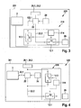
- the switching block 310 of the test block 320 in the illustrated fourth exemplary embodiment of the sensor unit 301 comprises a switching control logic 314, a first switching element 12.1 designed as a normally closed contact, which is looped into the connection 22.2 between the illustrated test connection contact 26 and the test circuit 22, and as Closer executed third switching element 12.3, via which the test circuit 22 of the test block 320 can be short-circuited to a reference potential 28.1, 28.2.
- the test circuit 22 is connected via the test connection 22. 1 directly to the function block 3 of the sensor unit 301 designed as an ASIC. Furthermore, the test circuit 22 is supplied with a supply voltage potential 28.1 and a ground potential 28.2 and driven by the test logic 24.
- connection connection 22.2 is separated by the first switching element 12.1 and the test connection contact 26 is switched off, which is arranged internally or led to the outside via a bond.
- the coupling structure is separated, via which EMC disturbances can reach the executed as ASIC sensor unit 1.
- the third closes Switching element 12.3 at the end of the manufacturing process, the test circuit 22 of the test block 320 with a reference potential 28.1, 28.2 briefly. In this case, the short circuit can take place either to the supply voltage potential 28.1 or to the ground potential 28.2. As a result, the EMC susceptibility of the sensor unit 301 can be further reduced.
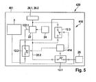
- the switching block 410 of the test block 420 in the illustrated fifth exemplary embodiment of the sensor unit 401 comprises a switching control logic 414, which is designed as normally closed first switching element 12.1, which is looped into the terminal connection 22.2 between the illustrated test terminal contact 26 and the test circuit 22, as normally closed executed second switching element 12.2, which is looped into the test connection 122.1 between the test circuit 22 and the function block 3 of ASIC designed as a sensor unit 201, and executed as normally open third switching element 12.3, via which the test circuit 22 of the test block 420 with a reference potential 28.1, 28.2 can be shorted. Furthermore, the test circuit 22 is supplied with a supply voltage potential 28.1 and a ground potential 28.2 and driven by the test logic 24.
- the connection 22.2 is disconnected after programming and the test terminal contact 26 is switched off.
- the coupling structure is separated, via which EMC disturbances can reach the executed as ASIC sensor unit 1.
- the third switching element 12.3 briefly closes the test circuit 22 of the test block 320 with a reference potential 28.1, 28.2.
- the short circuit can take place either to the supply voltage potential 28.1 or to the ground potential 28.2.
- the EMC susceptibility of the sensor unit 401 can be further reduced.
- the test circuit 22 is switched away from the function block 3 by the second switching element 12. 2 after programming.
- test connection 122.1 of the test circuit 22 is physically decoupled from the functional block 3 on the functional ASIC surface of the sensor unit 401 and, even in the event of a fault, can no longer contribute to any malfunctions or errors in the sensor unit 401.
- the second switching element 12.2 in the ASIC layout can be placed as close as possible to the functional ASIC surface to reduce potential points of failure.
- Embodiments of the present invention advantageously enable a broadband interference suppression of the EMC-sensitive test connection contacts via targeted switching off of the test connection contacts that are no longer required during normal operation of the sensor unit. Further, embodiments of the present invention can reduce the complexity of the sensor unit by selectively separating the candidate test blocks from the functional block and thereby also reduce the overall sensor error probability.
Landscapes
- Physics & Mathematics (AREA)
- Electromagnetism (AREA)
- Engineering & Computer Science (AREA)
- General Engineering & Computer Science (AREA)
- General Physics & Mathematics (AREA)
- Semiconductor Integrated Circuits (AREA)
- Testing Of Short-Circuits, Discontinuities, Leakage, Or Incorrect Line Connections (AREA)
- Testing Electric Properties And Detecting Electric Faults (AREA)
Description
- Die Erfindung geht aus von einer Sensoreinheit nach der Gattung des unabhängigen Patentanspruchs 1 und von einem Verfahren zur Bandendeprogrammierung einer Sensoreinheit nach der Gattung des unabhängigen Patentanspruchs 9.
- Ein Sensor misst eine physikalische Größe und übermittelt diese beispielsweise an eine zentrale Recheneinheit bzw. eine Regelungseinheit. Bei den bekannten Sensoren können Testschaltungen bzw. Testleitungen, wie beispielsweise Power-down-Leitungen für ein gezieltes Abschalten von Schaltungsblöcken, auf der ASIC-Fläche für den Testbetrieb eingesetzt werden, um eine hohe Testabdeckung der Sensoren zu erreichen. Diese Testschaltungen bzw. Testleitungen werden allein zum Zweck des Testens des ASICs (Application-Specific Integrated Circuit; Anwendungsspezifische Integrierte Schaltung) während des Fertigungsprozess des Sensors, beim Vormessen und/oder beim Endmessen aktiviert. Im Normalbetrieb des Sensors in der Applikation bleiben diese Testschaltungen/Testleitungen deaktiviert. Um die Sensoren beim Vormessen und/oder Endmessen auf ihre Soll-Parameter, wie beispielsweise Empfindlichkeit, Messbereich, Oszillatorabgleich usw., zu programmieren, können beispielsweise beim Vormessen Programmierpads auf ASIC-Level oder beim Endmessen im verpackten Zustand Programmierpins verwendet werden. Außerdem können zusätzliche Mess-Pads zur Eingabe von Digitalpattern usw. beim Vormessen zum Testen des ASICs verwendet werden.
- In der Offenlegungsschrift
DE 103 32 512 A1 wird beispielsweise eine Vorrichtung zum Beaufschlagen eines elektrischen Bauteils beschrieben. Die beschriebene Vorrichtung beaufschlagt das elektrische Bauteil mit mindestens einem eine dauerhafte Veränderung der elektrischen Eigenschaften des Bauteils herbeiführenden Energieimpuls. Die Vorrichtung umfasst mindestens ein den Energieimpuls leitendes elektrisches Leistungsschaltelement, das als Hochvolt-MOS-Transistor ausgeführt ist. Die beschriebene Vorrichtung kann beispielsweise zur Bandendeprogrammierung eines Produkts verwendet werden. Die Bandendeprogrammierung wird am Ende des Produktherstellungsprozesses dazu verwendet, um Produkten, welche in gleicher Weise hergestellt wurden, individuelle Merkmale zu verleihen. Dafür wird im Produkt mindestens ein Bauteil vorgesehen, welches während des Fertigungsprozesses zunächst bei allen Produkten gleich ausgebildet ist, dann aber am sogenannten Bandende, d.h. im letzten Fertigungsschritt, eine besondere Behandlung zur Einprägung von individuellen Merkmalen erfährt. So ist es beispielsweise bekannt, dass im Produkt Dioden vorgesehen werden, die mittels Beaufschlagung durch einen Energieimpuls in ihren elektrischen Eigenschaften verändert werden können. Durch eine im Produkt integrierte Detektionsvorrichtungen können solche Änderung der elektrischen Eigenschaften zu einem späteren Zeitpunkt festgestellt werden und mittels den von der Detektionsvorrichtung ermittelten Daten können dann bestimmte Merkmale oder Funktionen aktiviert bzw. deaktiviert werden oder aber zum Beispiel eine Seriennummer ausgegeben werden. - Aus der
US 2008/0157076 A1 ist eine Halbleiterschaltung mit Testanschlüssen und einer Anschlussvorrichtung bekannt, welche die Testanschlüsse während einer Testbetriebsart elektrisch mit einer integrierten Schaltung der Halbleiterschaltung verbindet. - Aus der
EP 1 970 720 A2 sind ein Halbleiterbauelement und ein Verfahren zum Testen eines solchen Halbleiterbauelements bekannt. Das Halbleiterbauelement weist auf einem Halbleiterchip mindestens ein Sensorelement zum Messen einer physikalischen Größe und eine Auswerteeinrichtung auf. Das Halbleiterbauelement ist zwischen einer ersten und zweiten Betriebsart umschaltbar. In einer ersten Betriebsart ist das Sensorelement für die zu messende physikalische Größe empfindlich und ein Messsignalausgang des Sensorelements ist mit einem Eingangsanschluss der Auswerteeinrichtung verbunden. In der zweiten Betriebsart ist das Sensorelement für die zu messende physikalische Größe unempfindlich und/oder der Signalpfad zwischen dem Messsignalausgang und dem Eingangsanschluss ist unterbrochen. Auf dem Halbleiterchip ist eine Testsignalquelle zur Erzeugung eines das Messsignal des Sensorelements simulierendes Testsignal angeordnet. Die Testsignalquelle ist in der zweiten Betriebsart mit dem Eingangsanschluss der Auswerteeinrichtung verbunden oder verbindbar. - Die erfindungsgemäße Sensoreinheit mit den Merkmalen des unabhängigen Patentanspruchs 1 und das erfindungsgemäße Verfahren zur Bandendeprogrammierung einer Sensoreinheit haben demgegenüber den Vorteil, dass eine breitbandige Entstörung von EMV-empfindlichen Testanschlusskontakten (EMV: elektromagnetische Verträglichkeit), welche Programmierpads, Programmierpins, Testpads, Testpins usw. umfassen können, über ein gezieltes Abschalten der im Normalbetrieb der Sensoreinheit nicht mehr erforderlichen Testanschlusskontakte ermöglicht wird. Hierdurch kann die Koppelstruktur abgetrennt werden, über welche die EMV-Störungen in die Sensoreinheit gelangen können. Des Weiteren können Ausführungsformen der vorliegenden Erfindung den Testblock vom Funktionsblock trennen und dadurch die Fehlerzahlen während der Sensorproduktion reduzieren. Zudem wird die Verbindung des Testblocks physikalisch von der funktionellen Fläche der Sensoreinheit entkoppelt, so dass der Testblock auch im Fehlerfall zu keinen Störungen bzw. Fehlern der Sensoreinheit beitragen kann. Durch das gezielte Trennen der in Frage kommenden Testblöcke vom Funktionsblock, kann die Komplexität der Sensoreinheit reduziert und dadurch auch die Gesamtwahrscheinlichkeit für einen Sensorfehler reduziert werden.
- Das Abschalten und/oder Trennen kann durch eine Bandendeprogrammierung am Ende der Sensorfertigung durchgeführt werden, wenn die Sensoreinheit vollständig programmiert und abgeglichen ist. Die Sensoreinheit ist vorzugsweise als ASIC ausgeführt. Das Abschalten und/oder Trennen kann dann über auf der ASIC-Fläche angeordnete Transistorlogikschaltungen realisiert werden.
- Ausführungsformen der vorliegenden Erfindung stellen eine Sensoreinheit mit mindestens einem Funktionsblock und mindestens einem Testblock zum Testen des mindestens einen Funktionsblocks zur Verfügung. Es ist ein Schaltblock mit mindestens einem Schaltelement vorgesehen, welcher am Ende des Fertigungsprozesses mindestens einen Testanschlusskontakt, welcher im Normalbetrieb der Sensoreinheit nicht erforderlich ist, vom Testblock trennt und/oder mindestens eine Testverbindung zwischen dem Testblock und dem Funktionsblock auftrennt.
- Erfindungsgemäß schließt der Schaltblock am Ende des Fertigungsprozesses den mindestens einen Testblock mit einem Bezugspotential kurz. Dadurch kann die EMV-Anfälligkeit der Sensoreinheit weiter reduziert werden. Hierbei ist darauf zu achten, dass die entstehende Schleife in Bezug auf die Fläche klein bleibt, da sich sonst eine neue Koppelstruktur ausbilden kann. Der mindestens eine Testblock kann beispielsweise zum Versorgungsspannungspotential oder zum Massepotential kurz geschlossen werden. Diese Maßnahme wird zusätzlich zur Trennung des mindestens einen Testanschlusskontakts vom Testblock durchgeführt, da das alleinige Kurzschließen des Testblocks mit einem Bezugspotential eher ungünstig ist, da sich EMV-Störungen von außen auf das Versorgungsspannungspotential oder das Massepotential der Sensoreinheit einkoppeln lassen und andere Funktionsblöcke der Sensoreinheit gestört werden können.
- Des Weiteren wird ein Verfahren zur Bandendeprogrammierung einer Sensoreinheit vorgeschlagen, welche mindestens einen Funktionsblock und mindestens einen Testblock zum Testen des mindestens einen Funktionsblocks aufweist. Hierbei wird am Ende des Fertigungsprozesses ein Testanschlusskontakt, welcher im Normalbetrieb der Sensoreinheit nicht erforderlich ist, vom Testblock getrennt. Zusätzlich oder alternativ kann mindestens eine Testverbindung zwischen dem Testblock und dem Funktionsblock aufgetrennt werden.
- Erfindungsgemäß schließt der Schaltblock am Ende des Fertigungsprozesses den mindestens einen Testblock mit einem Bezugspotential kurz.
- Ausführungsformen der vorliegenden Erfindung können flächenneutral und damit kostenneutral in die Sensoreinheit implementiert werden, da sie im Digitalteil realisiert werden können. Außerdem sind Ausführungsformen der vorliegenden Erfindung nicht toleranzbehaftet, unterliegen keinen Lebensdauereffekten und sind von außen nicht manipulierbar.
- Durch die in den abhängigen Ansprüchen aufgeführten Maßnahmen und Weiterbildungen sind vorteilhafte Verbesserungen der im unabhängigen Patentanspruch 1 angegebenen Sensoreinheit und des im unabhängigen Patentanspruch 9 angegebenen Verfahrens zur Bandendeprogrammierung einer Sensoreinheit möglich.
- In vorteilhafter Ausgestaltung der erfindungsgemäßen Sensoreinheit kann der Testblock beispielsweise eine Testschaltung und/oder eine Testlogik und/oder den mindestens einen Testanschlusskontakt umfassen. Hierbei kann die Testschaltung über die mindestens eine Testverbindung mit dem Funktionsblock und über mindestens eine Anschlussverbindung mit dem mindestens einen Testanschlusskontakt verbunden werden. Die Testlogik kann Ansteuersignale für die Testschaltung zum Testen und/oder Programmieren des Funktionsblocks erzeugen, wobei über den mindestens einen Testanschlusskontakt Signale zum Testen des Funktionsblocks eingegeben werden können.
- In weiterer vorteilhafter Ausgestaltung der erfindungsgemäßen Sensoreinheit kann der Schaltblock eine Schaltsteuerlogik zum Ansteuern des mindestens einen Schaltelements umfassen. Die Schaltsteuerlogik und die Testlogik können als gemeinsame Teststeuerlogik ausgeführt werden, wodurch der Flächenbedarf weiter reduziert werden kann.
- In weiterer vorteilhafter Ausgestaltung der erfindungsgemäßen Sensoreinheit ist das mindestens eine Schaltelement beispielsweise als Öffner zum Auftrennen einer korrespondierenden bestehenden Signalverbindung oder als Schließer zum Herstellen einer Signalverbindung ausgeführt.
- In weiterer vorteilhafter Ausgestaltung der erfindungsgemäßen Sensoreinheit ist das mindestens eine Schaltelement zum Auftrennen der mindestens einen Testverbindung zwischen dem Testblock und dem Funktionsblock im direkten Umfeld des Funktionsblocks angeordnet. Dadurch kann eine optimale Abschaltung ermöglicht und potentielle Angriffspunkte für Fehler bzw. Defekte können reduziert werden.
- Ausführungsbeispiele der Erfindung sind in den Zeichnungen dargestellt und werden in der nachfolgenden Beschreibung näher erläutert. In den Zeichnungen bezeichnen gleiche Bezugszeichen Komponenten bzw. Elemente, die gleiche bzw. analoge Funktionen ausführen.
- Kurze Beschreibung der Zeichnungen
-
Fig. 1 zeigt ein schematisches Blockdiagramm eines ersten Ausführungsbeispiels einer erfindungsgemäßen Sensoreinheit. -
Fig. 2 zeigt ein schematisches Blockdiagramm eines zweiten Ausführungsbeispiels einer erfindungsgemäßen Sensoreinheit. -
Fig. 3 zeigt ein schematisches Blockdiagramm eines dritten Ausführungsbeispiels einer erfindungsgemäßen Sensoreinheit. -
Fig. 4 zeigt ein schematisches Blockdiagramm eines vierten Ausführungsbeispiels einer erfindungsgemäßen Sensoreinheit. -
Fig. 5 zeigt ein schematisches Blockdiagramm eines fünften Ausführungsbeispiels einer erfindungsgemäßen Sensoreinheit. - Bei den bekannten Sensoren werden die nach außen geführten Test- bzw. Programmierpads in der Applikation für ein EMV-robustes Design entweder über eine auf dem ASIC ausgeführte Kapazität oder eine auf der Leiterplatte ausgeführte Kapazität oder direkt (niederohmig) auf ein bestimmtes Potential (meist Masse) gelegt oder offen gelassen. Die internen Test- und Programmierpads werden bei den bekannten Sensoren standardmäßig nicht befiltert oder terminiert.
- Durch das Vorhandensein der Testschaltungen bzw. Testleitungen steigt auch die Wahrscheinlichkeit von Qualitätsauffälligkeiten im Normalbetrieb des Sensors in der Applikation. Treten in diesen Testschaltungen bzw. Testleitungen Fehler bzw. Defekte auf, kann es zu einer Fehlfunktion des Sensors kommen. So können beispielsweise auch statistische ASIC-Fehler in Testschaltungen bzw. Testleitungen zu einem Sensordefekt führen, welcher als Qualitätsrückläufer in die Bandstatistik bzw. Feldstatistik eingeht.
- Das Fehlen der internen Befilterung bzw. von Terminierungen an Test- und Programmierpads kann zu EMV-Auffälligkeiten bei den Sensoren führen. ASIC interne Kapazitäten für die Befilterung der nach außen geführten Test- bzw. Programmierpads weisen den Nachteil auf, dass sie nicht flächenneutral und damit
- nicht kostenneutral sind. Zudem sind der internen Befilterung Grenzen in Bezug auf die maximale Fläche und damit der maximalen Kapazität gesetzt. Außerdem ist die Wirksamkeit der Kapazitäten über den Frequenzbereich begrenzt, d.h. die Kapazitäten sind bei bestimmten Frequenzen mehr oder weniger wirksam. Externe Entstörmaßnahmen über Kapazitäten sind möglich, aufgrund von Kosten und Platzbedarf auf der Leiterplatte jedoch nicht praktikabel. Außerdem kann sich die Bondinduktivität negativ auf die Wirksamkeit des Filters bzw. der Terminierung auswirken.
- Wie aus
Fig. 1 bis 5 ersichtlich ist, umfassen Ausführungsbeispiele einer erfindungsgemäßen Sensoreinheit 1, 101, 201, 301, 401 mindestens einen Funktionsblock 3. - Erfindungsgemäß ist ein Schaltblock 10, 110, 210, 310, 410 mit mindestens einem Schaltelement 12.1, 12.2, 12.3 vorgesehen, welcher am Ende des Fertigungsprozesses mindestens einen Testanschlusskontakt 26, welcher im Normalbetrieb der Sensoreinheit 1, 101, 201, 301, 401 nicht erforderlich ist, vom Testblock 20, 220, 320, 420 trennt und/oder mindestens eine Testverbindung 122.1 zwischen dem Testblock 120, 220, 420 und dem Funktionsblock 3 auftrennt.
- In den dargestellten Ausführungsbeispielen ist die Sensoreinheit 1, 101, 201, 301, 401 jeweils als ASIC (Application-Specific Integrated Circuit; Anwendungsspezifische Integrierte Schaltung) ausgeführt. Daher ist der jeweilige Schaltblock 10, 110, 210, 310, 410 mit den Schaltelementen 12.1, 12.2, 12.3 vorzugsweise als Transistorlogikschaltung auf dem ASIC realisiert. Dadurch ist der zusätzliche Schaltblock 10, 110, 210, 310, 410 flächenneutral und damit kostenneutral, da er im Digitalteil realisiert werden kann. Zudem ist der jeweilige Schaltblock 10, 110, 210, 310, 410 nicht toleranzbehaftet, unterliegt keinen Lebensdauereffekten und ist von außen nicht manipulierbar.
- Wie aus
Fig. 1 bis 5 weiter ersichtlich ist, umfasst der Testblock 20, 120, 220, 320, 420 in den dargestellten Ausführungsbeispielen jeweils eine Testschaltung 22, eine Testlogik 24 und den mindestens einen Testanschlusskontakt 26. Die Testschaltung 22 ist über die mindestens eine Testverbindung 22.1, 122.1 mit dem Funktionsblock 3 und über mindestens eine Anschlussverbindung 22.2, 122.2 mit dem mindestens einen Testanschlusskontakt 26 verbunden. Die Testlogik 24 erzeugt Ansteuersignale für die Testschaltung 22 zum Testen des Funktionsblocks 3. Über den mindestens einen Testanschlusskontakt 26 können Signale zum Testen des Funktionsblocks 3 eingegeben werden. - Wie aus
Fig. 1 bis 5 weiter ersichtlich ist, umfasst der Schaltblock 10, 110, 210, 310, 410 in den dargestellten Ausführungsbeispielen jeweils eine Schaltsteuerlogik 14, 114, 214, 314, 414 zum Ansteuern des mindestens einen Schaltelements 12.1, 12.2, 12.3. Bei einem alternativen nicht dargestellten Ausführungsbeispiel der erfindungsgemäßen Sensoreinheit 1, 101, 201, 301, 401 sind die Schaltsteuerlogik 14, 114, 214, 314, 414 und die Testlogik 24 als gemeinsame Teststeuerlogik ausgeführt. - Wie aus
Fig. 1 weiter ersichtlich ist, umfasst der Schaltblock 10 des Testblocks 20 im dargestellten ersten Ausführungsbeispiel der Sensoreinheit 1 eine Schaltsteuerlogik 14 und ein als Öffner ausgeführtes erstes Schaltelement 12.1, welches in die Anschlussverbindung 22.2 zwischen dem dargestellten Testanschlusskontakt 26 und der Testschaltung 22 eingeschleift ist. Die Testschaltung 22 ist über die Testverbindung 22.1 direkt mit dem Funktionsblock 3 der als ASIC ausgeführten Sensoreinheit 1 verbunden. Des Weiteren wird die Testschaltung 22 mit einem Versorgungsspannungspotential 28.1 und einem Massepotential 28.2 versorgt und von der Testlogik 24 angesteuert. Durch das erste Schaltelement 12.1 wird nach der Programmierung die Anschlussverbindung 22.2 aufgetrennt und der Testanschlusskontakt 26 weggeschaltet, welcher intern angeordnet oder über einen Bond nach außen geführt ist. Dadurch ist die Koppelstruktur abgetrennt, über welche EMV-Störungen in die als ASIC ausgeführte Sensoreinheit 1 gelangen können. - Wie aus
Fig. 2 weiter ersichtlich ist, umfasst der Schaltblock 110 des Testblocks 120 im dargestellten zwei Ausführungsbeispiel der Sensoreinheit 101 eine Schaltsteuerlogik 114 und ein als Öffner ausgeführtes zweites Schaltelement 12.2, welches in die Testverbindung 122.1 zwischen der Testschaltung 22 und dem Funktionsblock 3 der als ASIC ausgeführten Sensoreinheit 101 eingeschleift ist. Der dargestellte Testanschlusskontakt 26 ist über die Anschlussverbindung 22.2 direkt mit der Testschaltung 22 verbunden. Des Weiteren wird die Testschaltung 22 mit einem Versorgungsspannungspotential 28.1 und einem Massepotential 28.2 versorgt und von der Testlogik 24 angesteuert. Durch das zweite Schaltelement 12.2 wird nach der Programmierung die Testschaltung 22 vom Funktionsblock 3 weggeschaltet. Dadurch ist die Testverbindung 122.1 der Testschaltung physikalisch vom Funktionsblock 3 auf der funktionellen ASIC-Fläche der Sensoreinheit 101 entkoppelt und kann, auch im Fehlerfall, zu keinen Störungen bzw. Fehlern der Sensoreinheit 101 mehr beitragen. Für eine optimale Abschaltung kann das zweite Schaltelement 12.2 im ASIC Layout so dicht wie möglich an die funktionale ASIC-Fläche platziert werden, um potentielle Angriffspunkte für Fehler bzw. Defekte zu reduzieren. - Wie aus
Fig. 3 weiter ersichtlich ist, umfasst der Schaltblock 210 des Testblocks 220 im dargestellten dritten Ausführungsbeispiel der Sensoreinheit 201 eine Schaltsteuerlogik 214, das als Öffner ausgeführte erste Schaltelement 12.1, welches in die Anschlussverbindung 22.2 zwischen dem dargestellten Testanschlusskontakt 26 und der Testschaltung 22 eingeschleift ist, und das als Öffner ausgeführte zweite Schaltelement 12.2, welches in die Testverbindung 122.1 zwischen der Testschaltung 22 und dem Funktionsblock 3 der als ASIC ausgeführten Sensoreinheit 201 eingeschleift ist. Des Weiteren wird die Testschaltung 22 mit einem Versorgungsspannungspotential 28.1 und einem Massepotential 28.2 versorgt und von der Testlogik 24 angesteuert. Durch das erste Schaltelement 12.1 wird nach der Programmierung die Anschlussverbindung 22.2 aufgetrennt und der Testanschlusskontakt 26 weggeschaltet. Dadurch ist die Koppelstruktur abgetrennt, über welche EMV-Störungen in die als ASIC ausgeführte Sensoreinheit 1 gelangen können. Zusätzlich wird durch das zweite Schaltelement 12.2 nach der Programmierung die Testschaltung 22 vom Funktionsblock 3 weggeschaltet. Dadurch ist die Testverbindung 122.1 der Testschaltung physikalisch vom Funktionsblock 3 auf der funktionellen ASIC-Fläche der Sensoreinheit 201 entkoppelt und kann, auch im Fehlerfall, zu keinen Störungen bzw. Fehlern der Sensoreinheit 201 mehr beitragen. Für eine optimale Abschaltung kann das zweite Schaltelement 12.2 im ASIC Layout so dicht wie möglich an die funktionale ASIC-Fläche platziert werden, um potentielle Angriffspunkte für Fehler bzw. Defekte zu reduzieren. - Wie aus
Fig. 4 weiter ersichtlich ist, umfasst der Schaltblock 310 des Testblocks 320 im dargestellten vierten Ausführungsbeispiel der Sensoreinheit 301 eine Schaltsteuerlogik 314, ein als Öffner ausgeführtes erstes Schaltelement 12.1, welches in die Anschlussverbindung 22.2 zwischen dem dargestellten Testanschlusskontakt 26 und der Testschaltung 22 eingeschleift ist, und ein als Schließer ausgeführtes drittes Schaltelement 12.3, über welches die Testschaltung 22 des Testblocks 320 mit einem Bezugspotential 28.1, 28.2 kurzgeschlossen werden kann. Die Testschaltung 22 ist über die Testverbindung 22.1 direkt mit dem Funktionsblock 3 der als ASIC ausgeführten Sensoreinheit 301 verbunden. Des Weiteren wird die Testschaltung 22 mit einem Versorgungsspannungspotential 28.1 und einem Massepotential 28.2 versorgt und von der Testlogik 24 angesteuert. Durch das erste Schaltelement 12.1 wird nach der Programmierung die Anschlussverbindung 22.2 aufgetrennt und der Testanschlusskontakt 26 weggeschaltet, welcher intern angeordnet oder über einen Bond nach außen geführt ist. Dadurch ist die Koppelstruktur abgetrennt, über welche EMV-Störungen in die als ASIC ausgeführte Sensoreinheit 1 gelangen können. Zusätzlich schließt das dritte Schaltelement 12.3 am Ende des Fertigungsprozesses die Testschaltung 22 des Testblocks 320 mit einem Bezugspotential 28.1, 28.2 kurz. Hierbei kann der Kurzschluss entweder zum Versorgungsspannungspotential 28.1 oder zum Massepotential 28.2 erfolgen. Dadurch kann die EMV-Anfälligkeit der Sensoreinheit 301 weiter reduziert werden. - Wie aus
Fig. 5 weiter ersichtlich ist, umfasst der Schaltblock 410 des Testblocks 420 im dargestellten fünften Ausführungsbeispiel der Sensoreinheit 401 eine Schaltsteuerlogik 414, das als Öffner ausgeführte erste Schaltelement 12.1, welches in die Anschlussverbindung 22.2 zwischen dem dargestellten Testanschlusskontakt 26 und der Testschaltung 22 eingeschleift ist, das als Öffner ausgeführte zweite Schaltelement 12.2, welches in die Testverbindung 122.1 zwischen der Testschaltung 22 und dem Funktionsblock 3 der als ASIC ausgeführten Sensoreinheit 201 eingeschleift ist, und das als Schließer ausgeführte dritte Schaltelement 12.3, über welches die Testschaltung 22 des Testblocks 420 mit einem Bezugspotential 28.1, 28.2 kurzgeschlossen werden kann. Des Weiteren wird die Testschaltung 22 mit einem Versorgungsspannungspotential 28.1 und einem Massepotential 28.2 versorgt und von der Testlogik 24 angesteuert. Durch das erste Schaltelement 12.1 wird nach der Programmierung die Anschlussverbindung 22.2 aufgetrennt und der Testanschlusskontakt 26 weggeschaltet. Dadurch ist die Koppelstruktur abgetrennt, über welche EMV-Störungen in die als ASIC ausgeführte Sensoreinheit 1 gelangen können. Zusätzlich schließt das dritte Schaltelement 12.3 am Ende des Fertigungsprozesses die Testschaltung 22 des Testblocks 320 mit einem Bezugspotential 28.1, 28.2 kurz. Hierbei kann der Kurzschluss entweder zum Versorgungsspannungspotential 28.1 oder zum Massepotential 28.2 erfolgen. Dadurch kann die EMV-Anfälligkeit der Sensoreinheit 401 weiter reduziert werden. Des Weiteren wird durch das zweite Schaltelement 12.2 nach der Programmierung die Testschaltung 22 vom Funktionsblock 3 weggeschaltet. Dadurch ist die Testverbindung 122.1 der Testschaltung 22 physikalisch vom Funktionsblock 3 auf der funktionellen ASIC-Fläche der Sensoreinheit 401 entkoppelt und kann, auch im Fehlerfall, zu keinen Störungen bzw. Fehlem der Sensoreinheit 401 mehr beitragen. Für eine optimale Abschaltung kann das zweite Schaltelement 12.2 im ASIC Layout so dicht wie möglich an die funktionale ASIC-Fläche platziert werden, um potentielle Angriffspunkte für Fehler bzw. Defekte zu reduzieren. - Ausführungsformen der vorliegenden Erfindung ermöglichen in vorteilhafter Weise eine breitbandige Entstörung der EMV-empfindlichen Testanschlusskontakte über ein gezieltes Abschalten der im Normalbetrieb der Sensoreinheit nicht mehr erforderlichen Testanschlusskontakte. Des Weiteren können Ausführungsformen der vorliegenden Erfindung durch das gezielte Trennen der in Frage kommenden Testblöcke vom Funktionsblock die Komplexität der Sensoreinheit reduzieren und dadurch auch die Gesamtwahrscheinlichkeit für einen Sensorfehler reduzieren.
Claims (10)
- Sensoreinheit mit mindestens einem Funktionsblock (3) und mindestens einem Testblock (20, 120, 220, 320, 420) zum Testen des mindestens einen Funktionsblocks (3) und einem Schaltblock (10, 110, 210, 310, 410) mit mindestens einem Schaltelement (12.1, 12.2, 12.3), welcher mindestens eine Testverbindung (122.1) zwischen dem Testblock (120, 220, 420) und dem Funktionsblock (3) auftrennen kann, dadurch gekennzeichnet, dass der Schaltblock (310, 410) den mindestens einen Testblock (320, 420) mit einem Bezugspotential (28.1, 28.2) kurzschließen kann.
- Sensoreinheit nach Anspruch 1, dadurch gekennzeichnet, dass der Schaltblock (10, 110, 210, 310, 410) mindestens einen Testanschlusskontakt (26), welcher im Normalbetrieb der Sensoreinheit (1, 101, 201, 301, 401) nicht erforderlich ist, vom Testblock (20, 220, 320, 420) trennen kann.
- Sensoreinheit nach Anspruch 1 oder 2, dadurch gekennzeichnet, dass der Testblock (20, 120, 220, 320, 420) eine Testschaltung (22) und/oder eine Testlogik (24) und/oder den mindestens einen Testanschlusskontakt (26) umfasst, wobei die Testschaltung (22) über die mindestens eine Testverbindung (22.1, 122.1) mit dem Funktionsblock (3) und über mindestens eine Anschlussverbindung (22.2, 122.2) mit dem mindestens einen Testanschlusskontakt (26) verbunden ist, wobei die Testlogik (24) Ansteuersignale für die Testschaltung (22) zum Testen des Funktionsblocks (3) erzeugt, und wobei über den mindestens einen Testanschlusskontakt (26) Signale zum Testen des Funktionsblocks (3) eingebbar sind.
- Sensoreinheit nach einem der Ansprüche 1 bis 3, dadurch gekennzeichnet, dass der Schaltblock (10, 110, 210, 310, 410) eine Schaltsteuerlogik (14, 114, 214, 314, 414) zum Ansteuern des mindestens einen Schaltelements (12.1, 12.2, 12.3) umfasst.
- Sensoreinheit nach Anspruch 4, dadurch gekennzeichnet, dass die Schaltsteuerlogik (14, 114, 214, 314, 414) und die Testlogik (24) als gemeinsame Teststeuerlogik ausgeführt sind.
- Sensoreinheit nach einem der Ansprüche 1 bis 5, dadurch gekennzeichnet, dass das mindestens eine Schaltelement (12.1, 12.2, 12.3) als Öffner (12.1, 12.2) zum Auftrennen einer korrespondierenden bestehenden Signalverbindung (122.1, 22.2) oder als Schließer (12.3) zum Herstellen einer Signalverbindung ausgeführt ist.
- Sensoreinheit nach einem der Ansprüche 1 bis 6, dadurch gekennzeichnet, dass das mindestens eine Schaltelement (12.2) zum Auftrennen der mindestens einen Testverbindung (122.1) zwischen dem Testblock (120, 220, 420) und dem Funktionsblock (3) im direkten Umfeld des Funktionsblocks (3) angeordnet ist.
- Sensoreinheit nach einem der Ansprüche 1 bis 7, dadurch gekennzeichnet, dass die Sensoreinheit (1, 101, 201, 301, 401) als ASIC ausgeführt ist.
- Verfahren zur Bandendeprogrammierung einer Sensoreinheit, welche mindestens einen Funktionsblock (3) und mindestens einen Testblock (20, 120, 220, 320, 420) zum Testen des mindestens einen Funktionsblocks (3) aufweist, wobei am Ende des Fertigungsprozesses mindestens eine Testverbindung (122.1) zwischen dem Testblock (120, 220, 420) und dem Funktionsblock (3) aufgetrennt wird, dadurch gekennzeichnet, dass am Ende des Fertigungsprozesses der mindestens eine Testblock (320, 420) mit einem Bezugspotential (28.1, 28.2) kurzgeschlossen wird.
- Verfahren nach Anspruch 9, dadurch gekennzeichnet, dass am Ende des Fertigungsprozesses ein Testanschlusskontakt (26), welcher im Normalbetrieb der Sensoreinheit (1, 101, 201, 301, 401) nicht erforderlich ist, vom Testblock (20, 220, 320, 420) getrennt wird.
Applications Claiming Priority (2)
| Application Number | Priority Date | Filing Date | Title |
|---|---|---|---|
| DE102011084283A DE102011084283A1 (de) | 2011-10-11 | 2011-10-11 | Sensoreinheit und Verfahren zur Bandendeprogrammierung einer Sensoreinheit |
| PCT/EP2012/069822 WO2013053662A1 (de) | 2011-10-11 | 2012-10-08 | Sensoreinheit und verfahren zur bandendeprogrammierung einer sensoreinheit |
Publications (2)
| Publication Number | Publication Date |
|---|---|
| EP2766698A1 EP2766698A1 (de) | 2014-08-20 |
| EP2766698B1 true EP2766698B1 (de) | 2015-08-05 |
Family
ID=47177897
Family Applications (1)
| Application Number | Title | Priority Date | Filing Date |
|---|---|---|---|
| EP12784469.4A Not-in-force EP2766698B1 (de) | 2011-10-11 | 2012-10-08 | Sensoreinheit und verfahren zur bandendeprogrammierung einer sensoreinheit |
Country Status (4)
| Country | Link |
|---|---|
| EP (1) | EP2766698B1 (de) |
| CN (1) | CN103890549B (de) |
| DE (1) | DE102011084283A1 (de) |
| WO (1) | WO2013053662A1 (de) |
Families Citing this family (1)
| Publication number | Priority date | Publication date | Assignee | Title |
|---|---|---|---|---|
| US11181403B2 (en) * | 2019-09-24 | 2021-11-23 | Rosemount Inc. | Process variable sensor testing |
Family Cites Families (6)
| Publication number | Priority date | Publication date | Assignee | Title |
|---|---|---|---|---|
| US5895942A (en) * | 1996-06-18 | 1999-04-20 | Kabushiki Kaisha Toshiba | Fuse selectable modules |
| CH691237A5 (fr) * | 1997-07-15 | 2001-05-31 | Em Microelectronic Marin Sa | Photocapteur intégré. |
| DE19911526A1 (de) * | 1999-03-16 | 2000-09-21 | Bosch Gmbh Robert | Sensorüberwachung und Sensor mit Überwachungsschaltung |
| DE10332512A1 (de) | 2003-07-17 | 2005-02-03 | Robert Bosch Gmbh | Vorrichtung zum Beaufschlagen eines elektrischen Bauteils und Verwendung eines Leistungsschaltelements in genannter Vorrichtung |
| KR100794313B1 (ko) * | 2006-12-27 | 2008-01-11 | 삼성전자주식회사 | 범프 패드를 포함한 반도체 메모리 장치 및 그것의 테스트방법 |
| DE102007012214A1 (de) * | 2007-03-12 | 2008-09-18 | Micronas Gmbh | Halbleiterbauelement und Verfahren zum Testen eines solchen |
-
2011
- 2011-10-11 DE DE102011084283A patent/DE102011084283A1/de not_active Ceased
-
2012
- 2012-10-08 CN CN201280049689.6A patent/CN103890549B/zh not_active Expired - Fee Related
- 2012-10-08 WO PCT/EP2012/069822 patent/WO2013053662A1/de not_active Ceased
- 2012-10-08 EP EP12784469.4A patent/EP2766698B1/de not_active Not-in-force
Also Published As
| Publication number | Publication date |
|---|---|
| DE102011084283A1 (de) | 2013-04-11 |
| CN103890549B (zh) | 2016-09-14 |
| WO2013053662A1 (de) | 2013-04-18 |
| CN103890549A (zh) | 2014-06-25 |
| EP2766698A1 (de) | 2014-08-20 |
Similar Documents
| Publication | Publication Date | Title |
|---|---|---|
| DE102011003279B4 (de) | System und Verfahren zum Testen einer Schaltung | |
| EP3171124B2 (de) | Verfahren für den betrieb einer kapazitiven sensoranordnung eines kraftfahrzeugs | |
| EP1970720B1 (de) | Halbleiterbauelement und Verfahren zum Testen eines solchen | |
| DE102011005551A1 (de) | Belegungserkennungsvorrichtung zum Erkennen einer Belegung eines Sitzplatzes eines Kraftfahrzeuges | |
| EP4058816B1 (de) | Kontaktüberwachungsvorrichtung | |
| DE112019000888T5 (de) | System zur Erdung und Diagnose | |
| DE102005055954A1 (de) | Schaltungsanordnung und Verfahren zur Funktionsüberprüfung eines Leistungstransistors | |
| DE102009056395A1 (de) | Verfahren zur Funktionsprüfung von elektrischen Filtern sowie Filter mit Prüfeinrichtung | |
| DE102004051319B4 (de) | Einrichtung zum Steuern der Zündzeiteinstellung für Verbrennungsmotoren | |
| DE102021111771A1 (de) | Diagnosefähige Schaltungsanordnung, Sensorvorrichtung mit einer Schaltungsanordnung und Verfahren zur Diagnose einer Schaltungsanordnung und/oder Sensorvorrichtung | |
| EP2766698A1 (de) | Sensoreinheit und verfahren zur bandendeprogrammierung einer sensoreinheit | |
| DE19527744A1 (de) | Eingangsschaltung für einen Raddrehzahlsensor | |
| EP0646077B1 (de) | Schaltungsanordnung zur überwachung einer induktiven schaltung | |
| EP1989521B1 (de) | Schaltungsanordnung bzw. verfahren zur funktionsüberwachung eines vibrations-grenzschalters und/oder einer füllstand-messvorrichtung | |
| DE19831088C2 (de) | Schaltungsanordnung zur Überprüfung einer Tri-State-Erkennungsschaltung | |
| EP4490099A1 (de) | Kapazitiver sensor und verfahren zum betreiben eines kapazitiven sensors | |
| BE1029400B1 (de) | Kontaktüberwachungsvorrichtung für einen dreipoligen Wechselkontakt | |
| EP1423719B1 (de) | Verfahren und vorrichtung zum überwachen einer sensoreinheit | |
| EP0763877B1 (de) | Kommunikationssystem | |
| DE102006017260A1 (de) | Verfahren zur Schaltkreisüberprüfung | |
| DE102021111734A1 (de) | Diagnosefähige Schaltungsanordnung und Verfahren zur Diagnose einer Schaltungsanordnung | |
| EP1363477B1 (de) | Elektrische Schaltungsanordnung sowie Verfahren zur Überprüfung der Intaktheit eines Photodiodenarrays | |
| EP3298689A1 (de) | Signalverarbeitungseinrichtung und steuereinrichtung | |
| DE102023132611B3 (de) | Elektronisches Bauelement und Verfahren zum Betreiben eines solchen | |
| DE102023130908B3 (de) | Elektronische vorrichtung |
Legal Events
| Date | Code | Title | Description |
|---|---|---|---|
| PUAI | Public reference made under article 153(3) epc to a published international application that has entered the european phase |
Free format text: ORIGINAL CODE: 0009012 |
|
| 17P | Request for examination filed |
Effective date: 20140512 |
|
| AK | Designated contracting states |
Kind code of ref document: A1 Designated state(s): AL AT BE BG CH CY CZ DE DK EE ES FI FR GB GR HR HU IE IS IT LI LT LU LV MC MK MT NL NO PL PT RO RS SE SI SK SM TR |
|
| DAX | Request for extension of the european patent (deleted) | ||
| GRAP | Despatch of communication of intention to grant a patent |
Free format text: ORIGINAL CODE: EPIDOSNIGR1 |
|
| INTG | Intention to grant announced |
Effective date: 20150310 |
|
| GRAS | Grant fee paid |
Free format text: ORIGINAL CODE: EPIDOSNIGR3 |
|
| GRAA | (expected) grant |
Free format text: ORIGINAL CODE: 0009210 |
|
| AK | Designated contracting states |
Kind code of ref document: B1 Designated state(s): AL AT BE BG CH CY CZ DE DK EE ES FI FR GB GR HR HU IE IS IT LI LT LU LV MC MK MT NL NO PL PT RO RS SE SI SK SM TR |
|
| REG | Reference to a national code |
Ref country code: GB Ref legal event code: FG4D Free format text: NOT ENGLISH |
|
| REG | Reference to a national code |
Ref country code: CH Ref legal event code: EP |
|
| REG | Reference to a national code |
Ref country code: AT Ref legal event code: REF Ref document number: 740977 Country of ref document: AT Kind code of ref document: T Effective date: 20150815 |
|
| REG | Reference to a national code |
Ref country code: IE Ref legal event code: FG4D Free format text: LANGUAGE OF EP DOCUMENT: GERMAN |
|
| REG | Reference to a national code |
Ref country code: DE Ref legal event code: R096 Ref document number: 502012004051 Country of ref document: DE |
|
| REG | Reference to a national code |
Ref country code: LT Ref legal event code: MG4D |
|
| REG | Reference to a national code |
Ref country code: NL Ref legal event code: MP Effective date: 20150805 |
|
| PG25 | Lapsed in a contracting state [announced via postgrant information from national office to epo] |
Ref country code: LV Free format text: LAPSE BECAUSE OF FAILURE TO SUBMIT A TRANSLATION OF THE DESCRIPTION OR TO PAY THE FEE WITHIN THE PRESCRIBED TIME-LIMIT Effective date: 20150805 Ref country code: FI Free format text: LAPSE BECAUSE OF FAILURE TO SUBMIT A TRANSLATION OF THE DESCRIPTION OR TO PAY THE FEE WITHIN THE PRESCRIBED TIME-LIMIT Effective date: 20150805 Ref country code: LT Free format text: LAPSE BECAUSE OF FAILURE TO SUBMIT A TRANSLATION OF THE DESCRIPTION OR TO PAY THE FEE WITHIN THE PRESCRIBED TIME-LIMIT Effective date: 20150805 Ref country code: NO Free format text: LAPSE BECAUSE OF FAILURE TO SUBMIT A TRANSLATION OF THE DESCRIPTION OR TO PAY THE FEE WITHIN THE PRESCRIBED TIME-LIMIT Effective date: 20151105 Ref country code: GR Free format text: LAPSE BECAUSE OF FAILURE TO SUBMIT A TRANSLATION OF THE DESCRIPTION OR TO PAY THE FEE WITHIN THE PRESCRIBED TIME-LIMIT Effective date: 20151106 |
|
| PG25 | Lapsed in a contracting state [announced via postgrant information from national office to epo] |
Ref country code: PT Free format text: LAPSE BECAUSE OF FAILURE TO SUBMIT A TRANSLATION OF THE DESCRIPTION OR TO PAY THE FEE WITHIN THE PRESCRIBED TIME-LIMIT Effective date: 20151207 Ref country code: ES Free format text: LAPSE BECAUSE OF FAILURE TO SUBMIT A TRANSLATION OF THE DESCRIPTION OR TO PAY THE FEE WITHIN THE PRESCRIBED TIME-LIMIT Effective date: 20150805 Ref country code: SE Free format text: LAPSE BECAUSE OF FAILURE TO SUBMIT A TRANSLATION OF THE DESCRIPTION OR TO PAY THE FEE WITHIN THE PRESCRIBED TIME-LIMIT Effective date: 20150805 Ref country code: PL Free format text: LAPSE BECAUSE OF FAILURE TO SUBMIT A TRANSLATION OF THE DESCRIPTION OR TO PAY THE FEE WITHIN THE PRESCRIBED TIME-LIMIT Effective date: 20150805 Ref country code: IS Free format text: LAPSE BECAUSE OF FAILURE TO SUBMIT A TRANSLATION OF THE DESCRIPTION OR TO PAY THE FEE WITHIN THE PRESCRIBED TIME-LIMIT Effective date: 20151205 Ref country code: RS Free format text: LAPSE BECAUSE OF FAILURE TO SUBMIT A TRANSLATION OF THE DESCRIPTION OR TO PAY THE FEE WITHIN THE PRESCRIBED TIME-LIMIT Effective date: 20150805 Ref country code: HR Free format text: LAPSE BECAUSE OF FAILURE TO SUBMIT A TRANSLATION OF THE DESCRIPTION OR TO PAY THE FEE WITHIN THE PRESCRIBED TIME-LIMIT Effective date: 20150805 |
|
| PG25 | Lapsed in a contracting state [announced via postgrant information from national office to epo] |
Ref country code: NL Free format text: LAPSE BECAUSE OF FAILURE TO SUBMIT A TRANSLATION OF THE DESCRIPTION OR TO PAY THE FEE WITHIN THE PRESCRIBED TIME-LIMIT Effective date: 20150805 |
|
| PG25 | Lapsed in a contracting state [announced via postgrant information from national office to epo] |
Ref country code: DK Free format text: LAPSE BECAUSE OF FAILURE TO SUBMIT A TRANSLATION OF THE DESCRIPTION OR TO PAY THE FEE WITHIN THE PRESCRIBED TIME-LIMIT Effective date: 20150805 Ref country code: SK Free format text: LAPSE BECAUSE OF FAILURE TO SUBMIT A TRANSLATION OF THE DESCRIPTION OR TO PAY THE FEE WITHIN THE PRESCRIBED TIME-LIMIT Effective date: 20150805 Ref country code: EE Free format text: LAPSE BECAUSE OF FAILURE TO SUBMIT A TRANSLATION OF THE DESCRIPTION OR TO PAY THE FEE WITHIN THE PRESCRIBED TIME-LIMIT Effective date: 20150805 Ref country code: CZ Free format text: LAPSE BECAUSE OF FAILURE TO SUBMIT A TRANSLATION OF THE DESCRIPTION OR TO PAY THE FEE WITHIN THE PRESCRIBED TIME-LIMIT Effective date: 20150805 Ref country code: IT Free format text: LAPSE BECAUSE OF FAILURE TO SUBMIT A TRANSLATION OF THE DESCRIPTION OR TO PAY THE FEE WITHIN THE PRESCRIBED TIME-LIMIT Effective date: 20150805 |
|
| REG | Reference to a national code |
Ref country code: DE Ref legal event code: R119 Ref document number: 502012004051 Country of ref document: DE |
|
| PG25 | Lapsed in a contracting state [announced via postgrant information from national office to epo] |
Ref country code: RO Free format text: LAPSE BECAUSE OF FAILURE TO SUBMIT A TRANSLATION OF THE DESCRIPTION OR TO PAY THE FEE WITHIN THE PRESCRIBED TIME-LIMIT Effective date: 20150805 Ref country code: LU Free format text: LAPSE BECAUSE OF FAILURE TO SUBMIT A TRANSLATION OF THE DESCRIPTION OR TO PAY THE FEE WITHIN THE PRESCRIBED TIME-LIMIT Effective date: 20151008 |
|
| REG | Reference to a national code |
Ref country code: CH Ref legal event code: PL |
|
| PLBE | No opposition filed within time limit |
Free format text: ORIGINAL CODE: 0009261 |
|
| STAA | Information on the status of an ep patent application or granted ep patent |
Free format text: STATUS: NO OPPOSITION FILED WITHIN TIME LIMIT |
|
| PG25 | Lapsed in a contracting state [announced via postgrant information from national office to epo] |
Ref country code: MC Free format text: LAPSE BECAUSE OF FAILURE TO SUBMIT A TRANSLATION OF THE DESCRIPTION OR TO PAY THE FEE WITHIN THE PRESCRIBED TIME-LIMIT Effective date: 20150805 |
|
| 26N | No opposition filed |
Effective date: 20160509 |
|
| REG | Reference to a national code |
Ref country code: IE Ref legal event code: MM4A |
|
| PG25 | Lapsed in a contracting state [announced via postgrant information from national office to epo] |
Ref country code: DE Free format text: LAPSE BECAUSE OF NON-PAYMENT OF DUE FEES Effective date: 20160503 Ref country code: LI Free format text: LAPSE BECAUSE OF NON-PAYMENT OF DUE FEES Effective date: 20151031 Ref country code: CH Free format text: LAPSE BECAUSE OF NON-PAYMENT OF DUE FEES Effective date: 20151031 |
|
| REG | Reference to a national code |
Ref country code: FR Ref legal event code: ST Effective date: 20160630 |
|
| PG25 | Lapsed in a contracting state [announced via postgrant information from national office to epo] |
Ref country code: FR Free format text: LAPSE BECAUSE OF NON-PAYMENT OF DUE FEES Effective date: 20151102 Ref country code: SI Free format text: LAPSE BECAUSE OF FAILURE TO SUBMIT A TRANSLATION OF THE DESCRIPTION OR TO PAY THE FEE WITHIN THE PRESCRIBED TIME-LIMIT Effective date: 20150805 |
|
| PG25 | Lapsed in a contracting state [announced via postgrant information from national office to epo] |
Ref country code: IE Free format text: LAPSE BECAUSE OF NON-PAYMENT OF DUE FEES Effective date: 20151008 |
|
| PG25 | Lapsed in a contracting state [announced via postgrant information from national office to epo] |
Ref country code: BG Free format text: LAPSE BECAUSE OF FAILURE TO SUBMIT A TRANSLATION OF THE DESCRIPTION OR TO PAY THE FEE WITHIN THE PRESCRIBED TIME-LIMIT Effective date: 20150805 Ref country code: SM Free format text: LAPSE BECAUSE OF FAILURE TO SUBMIT A TRANSLATION OF THE DESCRIPTION OR TO PAY THE FEE WITHIN THE PRESCRIBED TIME-LIMIT Effective date: 20150805 Ref country code: HU Free format text: LAPSE BECAUSE OF FAILURE TO SUBMIT A TRANSLATION OF THE DESCRIPTION OR TO PAY THE FEE WITHIN THE PRESCRIBED TIME-LIMIT; INVALID AB INITIO Effective date: 20121008 |
|
| GBPC | Gb: european patent ceased through non-payment of renewal fee |
Effective date: 20161008 |
|
| PG25 | Lapsed in a contracting state [announced via postgrant information from national office to epo] |
Ref country code: CY Free format text: LAPSE BECAUSE OF FAILURE TO SUBMIT A TRANSLATION OF THE DESCRIPTION OR TO PAY THE FEE WITHIN THE PRESCRIBED TIME-LIMIT Effective date: 20150805 |
|
| PG25 | Lapsed in a contracting state [announced via postgrant information from national office to epo] |
Ref country code: GB Free format text: LAPSE BECAUSE OF NON-PAYMENT OF DUE FEES Effective date: 20161008 Ref country code: BE Free format text: LAPSE BECAUSE OF NON-PAYMENT OF DUE FEES Effective date: 20151031 |
|
| PG25 | Lapsed in a contracting state [announced via postgrant information from national office to epo] |
Ref country code: MT Free format text: LAPSE BECAUSE OF FAILURE TO SUBMIT A TRANSLATION OF THE DESCRIPTION OR TO PAY THE FEE WITHIN THE PRESCRIBED TIME-LIMIT Effective date: 20150805 |
|
| PG25 | Lapsed in a contracting state [announced via postgrant information from national office to epo] |
Ref country code: MK Free format text: LAPSE BECAUSE OF FAILURE TO SUBMIT A TRANSLATION OF THE DESCRIPTION OR TO PAY THE FEE WITHIN THE PRESCRIBED TIME-LIMIT Effective date: 20150805 |
|
| PG25 | Lapsed in a contracting state [announced via postgrant information from national office to epo] |
Ref country code: TR Free format text: LAPSE BECAUSE OF FAILURE TO SUBMIT A TRANSLATION OF THE DESCRIPTION OR TO PAY THE FEE WITHIN THE PRESCRIBED TIME-LIMIT Effective date: 20150805 Ref country code: AL Free format text: LAPSE BECAUSE OF FAILURE TO SUBMIT A TRANSLATION OF THE DESCRIPTION OR TO PAY THE FEE WITHIN THE PRESCRIBED TIME-LIMIT Effective date: 20150805 |
|
| REG | Reference to a national code |
Ref country code: AT Ref legal event code: MM01 Ref document number: 740977 Country of ref document: AT Kind code of ref document: T Effective date: 20171008 |
|
| PG25 | Lapsed in a contracting state [announced via postgrant information from national office to epo] |
Ref country code: AT Free format text: LAPSE BECAUSE OF NON-PAYMENT OF DUE FEES Effective date: 20171008 |