EP2765624A1 - Transparent conductive film, and organic light-emitting device comprising same - Google Patents
Transparent conductive film, and organic light-emitting device comprising same Download PDFInfo
- Publication number
- EP2765624A1 EP2765624A1 EP12885182.1A EP12885182A EP2765624A1 EP 2765624 A1 EP2765624 A1 EP 2765624A1 EP 12885182 A EP12885182 A EP 12885182A EP 2765624 A1 EP2765624 A1 EP 2765624A1
- Authority
- EP
- European Patent Office
- Prior art keywords
- emitting device
- light emitting
- layer
- organic light
- conducting film
- Prior art date
- Legal status (The legal status is an assumption and is not a legal conclusion. Google has not performed a legal analysis and makes no representation as to the accuracy of the status listed.)
- Withdrawn
Links
Images



Classifications
-
- H—ELECTRICITY
- H05—ELECTRIC TECHNIQUES NOT OTHERWISE PROVIDED FOR
- H05B—ELECTRIC HEATING; ELECTRIC LIGHT SOURCES NOT OTHERWISE PROVIDED FOR; CIRCUIT ARRANGEMENTS FOR ELECTRIC LIGHT SOURCES, IN GENERAL
- H05B33/00—Electroluminescent light sources
- H05B33/12—Light sources with substantially two-dimensional [2D] radiating surfaces
- H05B33/26—Light sources with substantially two-dimensional [2D] radiating surfaces characterised by the composition or arrangement of the conductive material used as an electrode
-
- C—CHEMISTRY; METALLURGY
- C01—INORGANIC CHEMISTRY
- C01G—COMPOUNDS CONTAINING METALS NOT COVERED BY SUBCLASSES C01D OR C01F
- C01G19/00—Compounds of tin
- C01G19/006—Compounds containing tin, with or without oxygen or hydrogen, and containing two or more other elements
-
- H—ELECTRICITY
- H10—SEMICONDUCTOR DEVICES; ELECTRIC SOLID-STATE DEVICES NOT OTHERWISE PROVIDED FOR
- H10K—ORGANIC ELECTRIC SOLID-STATE DEVICES
- H10K50/00—Organic light-emitting devices
- H10K50/80—Constructional details
- H10K50/805—Electrodes
- H10K50/81—Anodes
-
- H—ELECTRICITY
- H10—SEMICONDUCTOR DEVICES; ELECTRIC SOLID-STATE DEVICES NOT OTHERWISE PROVIDED FOR
- H10K—ORGANIC ELECTRIC SOLID-STATE DEVICES
- H10K50/00—Organic light-emitting devices
- H10K50/80—Constructional details
- H10K50/805—Electrodes
- H10K50/82—Cathodes
- H10K50/826—Multilayers, e.g. opaque multilayers
-
- H—ELECTRICITY
- H10—SEMICONDUCTOR DEVICES; ELECTRIC SOLID-STATE DEVICES NOT OTHERWISE PROVIDED FOR
- H10K—ORGANIC ELECTRIC SOLID-STATE DEVICES
- H10K50/00—Organic light-emitting devices
- H10K50/80—Constructional details
- H10K50/805—Electrodes
- H10K50/82—Cathodes
- H10K50/828—Transparent cathodes, e.g. comprising thin metal layers
-
- H—ELECTRICITY
- H10—SEMICONDUCTOR DEVICES; ELECTRIC SOLID-STATE DEVICES NOT OTHERWISE PROVIDED FOR
- H10K—ORGANIC ELECTRIC SOLID-STATE DEVICES
- H10K50/00—Organic light-emitting devices
- H10K50/80—Constructional details
- H10K50/85—Arrangements for extracting light from the devices
- H10K50/858—Arrangements for extracting light from the devices comprising refractive means, e.g. lenses
-
- C—CHEMISTRY; METALLURGY
- C01—INORGANIC CHEMISTRY
- C01P—INDEXING SCHEME RELATING TO STRUCTURAL AND PHYSICAL ASPECTS OF SOLID INORGANIC COMPOUNDS
- C01P2006/00—Physical properties of inorganic compounds
- C01P2006/40—Electric properties
-
- C—CHEMISTRY; METALLURGY
- C01—INORGANIC CHEMISTRY
- C01P—INDEXING SCHEME RELATING TO STRUCTURAL AND PHYSICAL ASPECTS OF SOLID INORGANIC COMPOUNDS
- C01P2006/00—Physical properties of inorganic compounds
- C01P2006/60—Optical properties, e.g. expressed in CIELAB-values
-
- H—ELECTRICITY
- H10—SEMICONDUCTOR DEVICES; ELECTRIC SOLID-STATE DEVICES NOT OTHERWISE PROVIDED FOR
- H10K—ORGANIC ELECTRIC SOLID-STATE DEVICES
- H10K50/00—Organic light-emitting devices
- H10K50/80—Constructional details
- H10K50/85—Arrangements for extracting light from the devices
- H10K50/854—Arrangements for extracting light from the devices comprising scattering means
Definitions
- the present invention relates to a transparent conducting film and an organic light emitting device comprising the same.
- An organic light emitting device is usually composed of two electrodes and an organic material layer of one or more layers disposed between the electrodes.
- the organic light emitting device If a voltage is applied between a first electrode and a second electrode in the organic light emitting device having the structure, holes and electrons flow from the first electrode and from the second electrode, respectively, into the organic material layer, the holes and electrons are recombined with each other to form an exciton, and a photon corresponding to an energy difference is emitted while the exciton falls back to the ground state.
- the organic light emitting device generates visible rays, and an information display device or illumination device may be manufactured by using this.
- the organic light emitting device may be manufactured by a method of depositing a first electrode on a substrate, depositing an organic material layer of one or more layers thereon, and then depositing a second electrode thereon. Therefore, in order to emit light generated from the organic material layer, an electrode in a direction to which the light is to be emitted needs to be transparent, and when light is to be emitted in the first electrode direction, the first electrode and also the substrate need to be transparent.
- an organic light emitting device that may prevent the loss of light due to the difference between refractive indices of a transparent electrode and a substrate to enhance the efficiency of the organic light emitting device, and a manufacturing method thereof.
- An exemplary embodiment of the present invention provides a transparent conducting film comprising: an indium tin oxide (ITO), wherein a ratio of integral intensity of a (222) plane in X-ray diffraction peaks (222), (400) and (440) is 70% or more.
- ITO indium tin oxide
- Another exemplary embodiment of the present invention provides a method for preparing a transparent conducting film, which comprises forming a transparent conducting film comprising an indium tin oxide (ITO) on a substrate, wherein a ratio of integral intensity of a (222) plane in X-ray diffraction peaks (222), (400) and (440) of the transparent conducting film is 70% or more.
- ITO indium tin oxide
- Yet another exemplary embodiment of the present invention provides an organic light emitting device comprising the transparent conducting film.
- the transparent conducting film according to the present invention has a low surface resistance value, a high front surface transmittance and a low light absorptance.
- the organic light emitting device according to the present invention may comprise a transparent conducting film having a low light absorptance to enhance the light emission efficiency.
- the organic light emitting device according to the present invention may additionally comprise an internal light extraction layer to improve the light extraction efficiency, and the loss of light generated by the difference between refractive indices of a transparent electrode and a substrate may be minimized.
- an organic light emitting device in which light is emitted in an anode direction as described above, light emitted from an organic material layer passes through the anode and is emitted in the air through a substrate.
- a glass having excellent air and moisture shielding characteristics is used, and the glass usually has a refractive index of approximately 1.5.
- the average refractive index of an organic material layer from which light is emitted is approximately 1.8.
- the refractive index of an organic material layer from which light is generated is approximately 1.8, and thus only light incident at an angle equal to or lower than a critical angle passes through a glass substrate having a refractive index of approximately 1.5, thereby generating a substantial loss of light.
- the phenomenon occurs even when light is emitted from the glass substrate to the air having a refractive index of 1.
- the method has a limitation that the effects may be exerted only on light transferred to the glass substrate among the light emitted from the organic material layer.
- a glass substrate having a refractive index of 1.8 or more is used to remove the refractive index interface between the organic material layer and the glass substrate, but the method is not appropriate for mass production.
- a device is manufactured, and then an external light extraction layer is attached to the surface of the device, or an internal light extraction layer is introduced into the device.
- the device internal progression path of light being released to the air during the driving of the organic light emitting device is elongated compared to a general organic light emitting device. Therefore, in an organic light emitting device into which the internal light extraction layer is introduced, the absorption factor of a material constituting the organic light emitting device affects the efficiency of the device more significantly than that of a general organic light emitting device.
- the present inventors have confirmed that an ITO having much better transparency and lower light absorptance than an ITO applied to a general organic light emitting device needs to be applied to an organic light emitting device in which an internal light extraction layer is formed, and have found that it serves a critical role in improving the efficiency of an organic light emitting device to which an internal light extraction layer is applied to minimize the light absorptance of the ITO.
- the transparent conducting film according to a specific example of the present invention comprises an indium tin oxide (ITO), in which the ratio of integral intensity of the (222) plane in X-ray diffraction peaks (222), (400) and (440) is 70% or more.
- ITO indium tin oxide
- the ratio of integral intensity of the (222) plane in the X-ray diffraction peaks (222), (400) and (440) of the transparent conducting film may be measured by the following Equation 1.
- the ratio of integral intensity of the 222 plane I 222 / I 222 + I 400 + I 440
- I 222 , I 400 and I 440 each represent the integral intensity of the X-ray diffraction peaks (222), (400) and (440) planes, respectively.
- the ratio of integral intensity of the (222) plane in the X-ray diffraction peaks (222), (400) and (440) of the transparent conducting film may be 70% or more, or 80% or more.
- the refractive index based on 550 nm of the transparent conducting film may be 1.9 or more, but is not limited thereto.
- the surface resistance value of the transparent conducting film may be from 20 ⁇ / ⁇ to 100 ⁇ / ⁇ , but is not limited thereto.
- the transparent conducting film according to the present invention has 70% or more of the ratio of integral intensity of the (222) plane in X-ray diffraction peaks (222), (400) and (440), in which the surface resistance value is low, the front surface transmittance is high, and the light absorptance is low.
- the light absorptance of the transparent conducting film according to the present invention may be 30% or less. In the present specification, the light absorptance may also be represented by the substrate absorption factor. Further, a method for preparing the transparent conducting film according to a specific example of the present invention comprises forming a transparent conducting film comprising an indium tin oxide (ITO) on a substrate, in which the ratio of integral intensity of the (222) plane in the X-ray diffraction peaks (222), (400) and (440) of the transparent conducting film is 70% or more.
- ITO indium tin oxide
- a deposition process may be used in the forming of the transparent conducting film, and the higher the partial pressure of oxygen in the deposition process, the higher the content of oxygen in the ITO gets, thereby increasing the (222) peak in the X-ray diffraction peaks. Accordingly, the surface resistance of the transparent conducting film is increased, and as the characteristics are changed as refractive index increases, the light absorptance tends to be decreased.
- the organic light emitting device comprises the transparent conducting film.
- the organic light emitting device may comprise a substrate, a first electrode comprising the transparent conducting film, an organic material layer of one or more layers, and a second electrode.
- the present invention may additionally comprise a light extraction layer between the substrate and the first electrode.
- the light extraction layer is not particularly limited as long as the layer has a structure in which light scattering may be induced to improve internal light extraction efficiency of the device.
- the light extraction layer may have a refractive index of 1.7 or more, and specifically comprise a range from 1.7 to 3.0.
- a material having a refractive index of 1.7 or more in the light extraction layer it is possible to obtain a light scattering effect due to the refractive index difference between one region of the material and another region having a relatively low refractive index.
- the light extraction layer may be a structure in which scattering particles are dispersed in a binder.
- the binder may have a refractive index higher than that of scattering particles, and it is possible to induce light scattering due to the difference in the refractive index at the interface of the binder and the scattering particles.
- the binder may have a refractive index in a range of 1.7 or more, or from 1.7 to 3.0.
- the light extraction layer comprises scattering particles and a binder, and may comprise a scattering layer on which unevenness is formed by scattering particles on the surface opposite to a surface contacting the substrate; and a flat layer which is formed on the scattering layer and flattens the surface bent due to the unevenness structure of the scattering layer.
- the light extraction layer may greatly exhibit the difference between refractive indices of scattering particles and the flat layer to enhance the internal light extraction efficiency.
- the flat layer may have a refractive index higher than that of the scattering particles, and for example, the flat layer may have a refractive index in a range of 1.7 or more, or from 1.7 to 3.0.
- the light extraction layer may comprise a binder layer which forms an unevenness structure and is formed on a substrate; and a flat layer which is formed on the binder layer to form a flat surface.
- the flat layer may have a refractive index in a range of 1.7 or more, or from 1.7 to 3.0.
- the scattering particles may be a spherical, elliptical, or amorphous shape, and preferably a spherical or elliptical shape.
- the scattering particles may have an average diameter from 100 nm to 300 nm, and specifically from 150 nm to 200 nm.
- the scattering particles are not particularly limited as long as the refractive index difference between the scattering particles and the binder to the flat layer may be used to scatter light, and may be one or more selected from the group consisting of air, silicon, silica, glass, titanium oxide, magnesium fluoride, zirconium oxide, alumina, cerium oxide, hafnium oxide, niobium pentoxide, tantalum pentoxide, indium oxide, tin oxide, indium tin oxide, zinc oxide, silicon, zinc sulfide, calcium carbonate, barium sulfate, silicon nitride and aluminum nitride.
- the scattering particles may be titanium dioxide.
- the binder is not particularly limited, and may be an organic, inorganic or organic and inorganic complex binder.
- the binder may be an inorganic or organic and inorganic complex binder.
- the inorganic or organic and inorganic complex binder has excellent heat resistance and chemical resistance compared to the organic binder, and thus the binder is advantageous in performance of the device, particularly, lifespan and deterioration, which may occur during the device manufacturing process, does not occur even during the high temperature process at 150°C or more, the photo process, the etching process and the like. Therefore, the binder is advantageous in the manufacture of various devices.
- the binder may be one or more selected from the group consisting of inorganic or organic and inorganic complexes and the like based on silicon oxide, silicon nitride, silicon oxynitride, alumina, and a siloxane bond (Si-O).
- Si-O siloxane bond
- the component constituting the flat layer may be selected in the same range as the binder constituting the scattering layer previously described.
- the same component may be used or other components may be used.
- the flat layer may further comprise a high refractive index filler which may increase the refractive index.
- the high refractive index filler is not particularly limited as long as the filler may be dispersed in a light extraction layer to increase the refractive index, and may be one or more selected from the group consisting of alumina, aluminum nitride, zirconium oxide, titanium oxide, cerium oxide, hafnium oxide, niobium pentoxide, tantalum pentoxide, indium oxide, tin oxide, indium tin oxide, zinc oxide, silicon, zinc sulfide, calcium carbonate, barium sulfate and silicon nitride.
- the high refractive filler may be titanium dioxide.
- the high refractive filler may have an average particle diameter from 5 nm to 30 nm, and specifically from 10 nm to 25 nm.
- the particle diameter of the high refractive filler is extremely small, it is difficult to disperse the filler in a solution, and as a result, the stability of a coating solution may deteriorate, and in the opposite case, transparency may be reduced or the surface after coating may become rough.
- the internal light extraction efficiency is improved by forming a light extraction layer comprising scattering particles on a substrate.
- the light extraction layer may be formed limitedly in a light emission region of the device toward a surface on which the device is deposited. Further, the light extraction layer may be a structure in which the light extraction layer is sealed by the substrate and the anode.
- the organic light emitting device in the related art, external air (for example, oxygen) or moisture may penetrate into the device through a path in which the light extraction layer is formed.
- the oxygen or moisture flowing into the device is responsible for reducing the service life of the device.
- the light extraction layer has a structure in which the layer is formed limitedly in a light emission region of the device, or is sealed by the substrate and the anode, and thus external air or moisture may be effectively prevented from penetrating into the device.
- the light extraction layer may be formed on a substrate by using a coating solution comprising scattering particles and a binder.
- the scattering particles form a structure in which the particles are dispersed in the binder.
- the refractive index of the binder is not particularly limited, but may be, for example, 1.7 or more.
- the light extraction layer may be formed by using a method comprising: using a coating solution comprising scattering particles and a binder on a substrate to form a scattering layer; and forming a flat layer on the formed scattering layer.
- the refractive index of the flat layer is not particularly limited, but may be, for example, 1.7 or more.
- the light extraction layer may be formed by using a method comprising: forming an unevenness structure on a substrate through micro-embossing; and forming a flat layer which flattens the surface on the formed unevenness structure.
- the unevenness structure is formed by applying a coating solution comprising a binder on a substrate and subjecting the substrate to a micro-embossing process. Thereafter, a relatively high refractive index flat layer may be formed on the formed unevenness structure to constitute a light extraction layer.
- the refractive index of the flat layer may be, for example, 1.7 or more.
- the light extraction layer may be implemented by CVD (chemical vapor deposition), PVD (physical vapor deposition) or a sol-gel coating, and the method is not particularly limited.
- the present inventors have confirmed that the loss of light frequently occurs even in the cathode, and have studied a method for preventing the loss of light generated from the cathode.
- the organic light emitting device sequentially comprises a substrate, an anode comprising the transparent conducting film, an organic material layer of one or more layers, a first cathode comprising a first metal, and a second cathode comprising a second metal, in which based on a wavelength of 550 nm, the refractive index (n 1 ) of the first metal is in a range of the following Equation 2, the absorptivity coefficient (k) of the first metal is in a range of 5 or less, and a light extraction layer is comprised between the substrate and the anode.
- Equation 2 n1 represents the refractive index of the first metal and k represents the absorptivity coefficient of the first metal.
- the organic light emitting device may comprise a cathode with a double-layer structure to increase the reflectance of the cathode, and accordingly, it is possible to minimize the loss of light generated due to the refractive index difference between a transparent electrode and a substrate and to enhance the light emission efficiency of an organic light emitting device, particularly, an organic light emitting device used for illumination.
- the loss of light may be minimized by comprising a first metal having a low absorption factor and a high reflectance in a first cathode contacting an organic material layer.
- the reflectance (R) of light incident on the front surface of the metal may be calculated by the following Equation 3.
- R n - n 0 2 + k 2 n + n 0 2 + k 2
- Equation 3 n0 represents the refractive index of the entrance medium, n is the refractive index of the metal, and k represents the absorption coefficient of the metal.
- Equation 3 it can be known that as the refractive index (n) of the metal approaches 0, the reflectance of the metal is increased, and as the absorptivity coefficient (k) of the metal is increased, the reflectance is increased. In addition, as the refractive index of the entrance medium is increased, the reflectance of the metal is decreased, and thus the metal is disadvantageous in an organic light emitting device.
- the refractive index (n 1 ) of the first metal is in a range of the following Equation 2 and the absorptivity coefficient (k) of the first metal is in a range of 5 or less, based on a wavelength of 550 nm. 23.73 - 500 - k 2 - 0.2 ⁇ n 1 ⁇ 23.73 - 500 - k 2 + 0.2
- the first cathode comprising the first metal may have a structure of contacting the organic material layer of one or more layers.
- the first metal comprised in the first cathode and the second metal comprised in the second cathode may be different metals.
- Examples of the first metal comprise Cu, Au, Li, Ag and the like, but are not limited thereto.
- the thickness of the first cathode may be from 1 nm to 100 nm and from 1 nm to 50 nm, but is not limited thereto.
- the reflectance of light incident on the front surface of the first cathode may be 70% or more and 80% or more, but is not limited thereto.
- the reflectance may be calculated by Equation 2.
- the second cathode comprises the second metal
- the second metal may be one or more selected from magnesium, calcium, sodium, potassium, titanium, indium, yttrium, lithium, gadolinium, aluminum, silver, platinum, gold, tungsten, tantalum, copper, tin and lead.
- the second metal is preferably aluminum or silver.
- the thickness of the second cathode may be from 50 nm to 5 ⁇ m, but is not limited thereto.
- Al has a refractive index of 1.015 at 550 nm, and an absorptivity coefficient of 6.627.
- the reflectance of the surface of Al in the air having a refractive index of 1 is at a level of 91.5% according to Equation 3, which is a very high value.
- the reflected surface of Al does not contact the air, but an organic material having a refractive index of about 1.8. At this time, the reflectance of Al is reduced to 85.9%.
- light is reflected on the surface of Al while circulating the organic material layer several times, and at each time of the reflection, light is lost by about 14%. When the loss is reduced, the extraction effect through an internal light extraction layer is increased, and thus it is very important not only to develop an internal light extraction layer, but also to reduce the absorption factor of the OLED itself.
- the probability of short occurrence is a phenomenon linked to the case in which the cathode and the anode are at a low-resistance level due to defects on the substrate of the device, and the probability of occurrence of defects is proportional to the area of a substrate, and the OLED is particularly disadvantageous in an illumination in which a single cell is formed to have a very large area.
- a first metal having a refractive index and an absorptivity coefficient in the range described above in front of the Al cathode is formed with a thin thickness, and it is possible to obtain a reflectance higher than that of the first metal itself or Al by the configuration.
- the first cathode and the second cathode may be formed by using any one physical vapor deposition (PVD) selected from sputtering, E-beam evaporation, thermal evaporation, laser molecular beam epitaxy (L-MBE), and pulsed laser deposition (PLD); any one chemical vapor deposition selected from thermal chemical vapor deposition, plasma-enhanced chemical vapor deposition (PECVD), light chemical vapor deposition, laser chemical vapor deposition, metal-organic chemical vapor deposition (MOCVD), and hydride vapor phase epitaxy (HVPE); or atomic layer deposition (ALD).
- PVD physical vapor deposition
- PECVD plasma-enhanced chemical vapor deposition
- MOCVD metal-organic chemical vapor deposition
- HVPE hydride vapor phase epitaxy
- ALD atomic layer deposition
- the first metal may be Li and the second metal may be Al or Ag.
- a substrate known in the art may be used without limitation, and more specific examples thereof comprise a glass substrate, a plastic substrate and the like, but are not limited thereto.
- the present invention may additionally comprise an auxiliary electrode in order to improve the resistance of the anode.
- the auxiliary electrode may be formed by depositing one or more selected from the group consisting of conducting sealants and metals, and then using a photo process or a printing process. More specifically, the auxiliary electrode may comprise Cr, Mo, Al, Cu, an alloy thereof and the like, but is not limited thereto.
- the present invention may additionally comprise an insulating layer on the auxiliary electrode.
- the insulating layer may be formed by using a material and a method known in the art. More specifically, the insulating layer may be formed by using a general photoresist material; polyimide; polyacryl; silicon nitride; silicon oxide; aluminum oxide; aluminum nitride; an alkali metal oxide; an alkaline earth metal oxide, and the like, but is not limited thereto.
- the thickness of the insulating layer may be from 10 nm to 10 ⁇ m, but is not limited thereto.
- the organic material layer may be manufactured with fewer layers by using various polymer materials by a solvent process other than a deposition method, for example, a method, such as spin coating, dip coating, doctor blading, screen printing, inkjet printing, thermal transfer or the like.
- a solvent process other than a deposition method, for example, a method, such as spin coating, dip coating, doctor blading, screen printing, inkjet printing, thermal transfer or the like.
- the organic material layer according to the present invention may have a stacked structure in which the organic material layer comprises a light emitting layer, and one or more selected from a hole injection layer, a hole transporting layer, an electron transporting layer and an electron injection layer.
- a material capable of forming the hole injection layer is preferably a material having a large work function such that the injection of holes into the organic material layer may be usually facilitated.
- the hole injection material which may be used in the present invention comprise metals such as vanadium, chromium, copper, zinc and gold, or alloys thereof; metal oxides such as zinc oxide, indium oxide, indium tin oxide (ITO) and indium zinc oxide (IZO); a combination of metal and oxide, such as ZnO : Al or SnO 2 : Sb; electrically conductive polymers, such as poly(3-methylthiophene), poly[3,4-(ethylene-1,2-dioxy)thiophene](PEDT), polypyrrole and polyaniline, and the like, but are not limited thereto.
- a material capable of forming the electron injection layer is preferably a material having a small work function such that electrons are usually easily injected into the organic material layer.
- the electron injection material comprise metals such as magnesium, calcium, sodium, potassium, titanium, indium, yttrium, lithium, gadolinium, aluminum, silver, tin and lead, or alloys thereof; multi-layer structured materials such as LiF/Al or LiO 2 /Al, and the like, the same material as the hole injection electrode material may be used, but the materials are not limited thereto.
- a material capable of forming the light emitting layer is a material that is capable of emitting light in a visible ray region by accepting and recombining holes from the hole transporting layer and electrons from the electron transporting layer, respectively, and is preferably a material having high quantum efficiency for fluorescence and phosphorescence.
- Specific examples thereof comprise 8-hydroxy-quinoline-aluminum complex (Alq 3 ); carbazole-based compounds; dimerized styryl compounds; BAlq; 10-hydroxybenzoquinoline-metal compounds; benzoxazole-based, benzthiazole-based and benzimidazole-based compounds; poly(p-phenylenevinylene)(PPV)-based polymers; spiro compounds; polyfluorene and rubrene; phosphorescence host CBP[[4,4'-bis(9-carbazolyl)biphenyl] and the like, but are not limited thereto.
- Alq 3 8-hydroxy-quinoline-aluminum complex
- carbazole-based compounds dimerized styryl compounds
- BAlq 10-hydroxybenzoquinoline-metal compounds
- benzoxazole-based, benzthiazole-based and benzimidazole-based compounds poly(p-phenylenevinylene)(PPV)-based polymers
- the light emission material may additionally comprise a phosphorescent dopant or fluorescent dopant in order to improve fluorescent or phosphorescent characteristics.
- a phosphorescent dopant comprise ir(ppy)(3)[fac tris(2-phenylpyridine) iridium], F2Irpic[iridium(III)bis(4,6,-di-fluorophenyl-pyridinato-N,C2) picolinate] or the like.
- the fluorescent dopant materials known in the art may be used.
- a material capable of forming the electron transporting layer a material which may receive electrons from the electron injection layer and transport the electrons to the light emitting layer well and having high mobility to electrons is suitable.
- Specific examples thereof comprise aluminum complexes of 8-hydroxyquinoline; complexes comprising Alq 3 ; organic radical compounds; hydroxyflavone-metal complexes, and the like, but are not limited thereto.
- the organic light emitting device according to the present invention may be more preferably applied to an organic light emitting device for illumination.
- the following deposition apparatus and deposition condition were used to deposit ITO on a glass substrate.
- An internal light extraction layer was formed on a glass substrate, and then the deposition apparatus and deposition conditions in 1) were used to deposit an ITO thereon. Thereafter, a photo process was performed and an organic light emitting device was manufactured.
- TiO 2 particles having an average particle diameter of about 200 nm were sufficiently dispersed in a siloxane binder solution to prepare a coating solution.
- the prepared coating solution was applied on a glass substrate to form a scattering layer.
- a siloxane binder (a refractive index of about 1.8 after drying), in which a high refractive index filler (TiO 2 ) having an average particle diameter of about 10 nm was dispersed, was coated on the scattering layer to form a high refractive index coating layer having a flat surface. Through this, a light extraction layer was formed on the glass substrate.
- a first transparent electrode, an organic material layer and a second electrode were sequentially stacked on the prepared internal light extraction layer to manufacture a white OLED having a light emitting region of 40 x 40 mm 2 .
- ITO Indium Tin Oxide
- Al aluminum
- the organic layer was formed as a structure comprising a hole injection layer, an hole transferring layer, an organic light emitting layer, an electron transferring layer and an electron injection layer.
- materials typically used in the manufacturing field of white OLEDs were used, and as the formation method thereof, a general method was also used.
- the front surface transmittances of the ITO deposited substrates according to Examples 1 to 3 and Comparative Example 1 are shown in the following FIG. 3
- the X-ray diffraction peaks of the ITO deposited substrates are shown in the following FIG. 4 .
- Bruker AXS D4 Endeavor XRD (2) was used as an apparatus which evaluated the X-ray diffraction. Furthermore, an integrating sphere was used to measure the substrate absorption factor. More specifically, if a brightness of the integrating sphere while a magnetic absorption calibration lamp in the integrating sphere is lit is defined as L 0 , a brightness of the integrating sphere when a sample to be measured in the integrating sphere is disposed in the middle thereof is defined as Ls, and a brightness of integrating sphere when a complete absorption body having the same size as the sample in the integrating sphere is disposed in the middle thereof is defined as L D , the substrate absorption factor may be calculated by the following Equation 4.
- the absorption factor of the substrate When the absorption factor of the substrate is measured, a more accurate result may be obtained by using a substrate on which an internal light extraction layer is formed as in the Examples rather than a substrate that is deposited on a transparent glass (bare glass).
- a substrate on which an internal light extraction layer is formed When a substrate on which an internal light extraction layer is formed is used, the optical path in the substrate is formed at various angles. Accordingly, the absorption factor of the ITO may be confirmed in an environment similar to the environment during the actual emission of the device, and light is absorbed in a relatively large amount, thereby increasing the discrimination between samples to be measured.
- Substrate absorption factor % 1 - Ls - L D / L 0 - L D ⁇ 100
- the following deposition apparatus and deposition condition were used to deposit ITO on a glass substrate.
- An internal light extraction layer was formed on a glass substrate, and then the deposition apparatus and deposition conditions in 1) were used to deposit an ITO thereon. Thereafter, a photo process was performed and an organic light emitting device was manufactured.
- TiO 2 particles having an average particle diameter of about 200 nm were sufficiently dispersed in a siloxane binder solution to prepare a coating solution.
- the prepared coating solution was applied on a glass substrate to form a scattering layer.
- a siloxane binder (a refractive index of about 1.8 after drying), in which a high refractive index filler (TiO 2 ) having an average particle diameter of about 10 nm was dispersed, was coated on the scattering layer to form a high refractive index coating layer having a flat surface. Through this, a light extraction layer was formed on the glass substrate.
- a first transparent electrode, an organic material layer and a second electrode were sequentially stacked on the prepared internal light extraction layer to manufacture a white OLED having a light emitting region of 40 x 40 mm 2 .
- ITO Indium Tin Oxide
- Al aluminum
- the organic layer was formed as a structure comprising a hole injection layer, a hole transferring layer, an organic light emitting layer, an electron transferring layer and an electron injection layer.
- materials typically used in the manufacturing field of white OLEDs were used, and as the formation method thereof, a general method was also used.
- the front surface transmittances of the ITO deposited substrates according to Examples 4 to 7 and Comparative Example 1 are shown in the following FIG. 5
- the X-ray diffraction peaks of the ITO deposited substrates are shown in the following FIG. 6 .
- the transparent conducting film according to the present invention has a low surface resistance value and a low light absorptance.
- the light emission efficiency of the organic light emitting device according to the present invention may be enhanced by comprising a transparent conducting film having low light absorptance.
- the organic light emitting device according to the present invention may additionally comprise an internal light extraction layer to improve the light extraction efficiency, and the loss of light generated by the difference between refractive indices of a transparent electrode and a substrate may be minimized.
Landscapes
- Physics & Mathematics (AREA)
- Optics & Photonics (AREA)
- Chemical & Material Sciences (AREA)
- Organic Chemistry (AREA)
- Inorganic Chemistry (AREA)
- Electroluminescent Light Sources (AREA)
- Non-Insulated Conductors (AREA)
- Manufacturing Of Electric Cables (AREA)
Abstract
Description
- The present invention relates to a transparent conducting film and an organic light emitting device comprising the same.
- This application claims priority from Korean Patent Application No.
10-2012-0101513, filed November 14, 2012 - An organic light emitting device (OLED) is usually composed of two electrodes and an organic material layer of one or more layers disposed between the electrodes.
- If a voltage is applied between a first electrode and a second electrode in the organic light emitting device having the structure, holes and electrons flow from the first electrode and from the second electrode, respectively, into the organic material layer, the holes and electrons are recombined with each other to form an exciton, and a photon corresponding to an energy difference is emitted while the exciton falls back to the ground state. By this principle, the organic light emitting device generates visible rays, and an information display device or illumination device may be manufactured by using this.
- In general, the organic light emitting device may be manufactured by a method of depositing a first electrode on a substrate, depositing an organic material layer of one or more layers thereon, and then depositing a second electrode thereon. Therefore, in order to emit light generated from the organic material layer, an electrode in a direction to which the light is to be emitted needs to be transparent, and when light is to be emitted in the first electrode direction, the first electrode and also the substrate need to be transparent.
- In the art to which the present invention belongs, it is necessary to study an organic light emitting device that may prevent the loss of light due to the difference between refractive indices of a transparent electrode and a substrate to enhance the efficiency of the organic light emitting device, and a manufacturing method thereof.
- An exemplary embodiment of the present invention provides a transparent conducting film comprising: an indium tin oxide (ITO), wherein a ratio of integral intensity of a (222) plane in X-ray diffraction peaks (222), (400) and (440) is 70% or more.
- Another exemplary embodiment of the present invention provides a method for preparing a transparent conducting film, which comprises forming a transparent conducting film comprising an indium tin oxide (ITO) on a substrate, wherein a ratio of integral intensity of a (222) plane in X-ray diffraction peaks (222), (400) and (440) of the transparent conducting film is 70% or more.
- Yet another exemplary embodiment of the present invention provides an organic light emitting device comprising the transparent conducting film.
- The transparent conducting film according to the present invention has a low surface resistance value, a high front surface transmittance and a low light absorptance. The organic light emitting device according to the present invention may comprise a transparent conducting film having a low light absorptance to enhance the light emission efficiency. In particular, the organic light emitting device according to the present invention may additionally comprise an internal light extraction layer to improve the light extraction efficiency, and the loss of light generated by the difference between refractive indices of a transparent electrode and a substrate may be minimized.
-
-
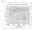
FIG. 1 is a graph showing the front surface transmittances of ITO deposited substrates in the related art. -
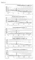
FIG. 2 is a view illustrating the X-ray diffraction peaks of ITO deposited substrates in the related art. -
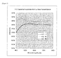
FIG. 3 is a graph showing the front surface transmittances of ITO deposited substrates according to Examples 1 to 3 and Comparative Example 1 of the present invention. -
FIG. 4 is a view illustrating the X-ray diffraction peaks of ITO deposited substrates according to Examples 1 to 3 and Comparative Example 1 of the present invention. -
FIG. 5 is a graph showing the front surface transmittances of ITO deposited substrates according to Examples 4 to 7 and Comparative Example 2 of the present invention. -
FIG. 6 is a view illustrating the X-ray diffraction peaks of ITO deposited substrates according to Examples 4 to 7 and Comparative Example 2 of the present invention. - Hereinafter, the present invention will be described in detail.
- In the case of illumination requiring a wide light emission area unlike displays, development is generally underway toward a structure to emit light in an anode direction. This is because it has a technical limitation to increase electrical conductivity of a transparent electrode, and thus a transparent electrode of an organic light emitting device for illumination needs a metal auxiliary electrode, and as a result, it is technically much easier to form a metal auxiliary electrode on the anode side than to form a metal auxiliary electrode on the cathode side.
- In the case of an organic light emitting device in which light is emitted in an anode direction as described above, light emitted from an organic material layer passes through the anode and is emitted in the air through a substrate. As the substrate, a glass having excellent air and moisture shielding characteristics is used, and the glass usually has a refractive index of approximately 1.5. In contrast, it is known that the average refractive index of an organic material layer from which light is emitted is approximately 1.8.
- When light generally proceeds from a medium having a high refractive index into a medium having a low refractive index, a phenomenon that light incident at an angle equal to or higher than a critical angle fails to pass through the medium having a low refractive index and is totally reflected occurs. Therefore, even in the case of the organic light emitting device, the refractive index of an organic material layer from which light is generated is approximately 1.8, and thus only light incident at an angle equal to or lower than a critical angle passes through a glass substrate having a refractive index of approximately 1.5, thereby generating a substantial loss of light. The phenomenon occurs even when light is emitted from the glass substrate to the air having a refractive index of 1.
- Therefore, it is necessary to study an external light extraction in order to improve the efficiency of an organic light emitting device by preventing the light from being totally reflected in the transparent substrate without being released from the transparent substrate to the air layer among the loss of light generated at the interface between media having different refractive indices as described above and from being extinguished, thereby improving the efficiency of the organic light emitting device.
- As an example, there is a method of modifying the surface of a flat glass substrate in order to prevent the loss of light generated at the interface between the glass substrate and the air. A substantial amount of light extinguished by the total reflection in the glass substrate by the above-described method may be recovered to improve the efficiency of the organic light emitting device. However, the method has a limitation that the effects may be exerted only on light transferred to the glass substrate among the light emitted from the organic material layer. In order to transfer all the light emitted from the organic material layer to the glass substrate, a glass substrate having a refractive index of 1.8 or more is used to remove the refractive index interface between the organic material layer and the glass substrate, but the method is not appropriate for mass production.
- In order to improve the efficiency of an organic light emitting device in the related art, a device is manufactured, and then an external light extraction layer is attached to the surface of the device, or an internal light extraction layer is introduced into the device.
- In an organic light emitting device into which an internal light extraction layer is introduced, the device internal progression path of light being released to the air during the driving of the organic light emitting device is elongated compared to a general organic light emitting device. Therefore, in an organic light emitting device into which the internal light extraction layer is introduced, the absorption factor of a material constituting the organic light emitting device affects the efficiency of the device more significantly than that of a general organic light emitting device.
- Thus, the present inventors have confirmed that an ITO having much better transparency and lower light absorptance than an ITO applied to a general organic light emitting device needs to be applied to an organic light emitting device in which an internal light extraction layer is formed, and have found that it serves a critical role in improving the efficiency of an organic light emitting device to which an internal light extraction layer is applied to minimize the light absorptance of the ITO.
- The transparent conducting film according to a specific example of the present invention comprises an indium tin oxide (ITO), in which the ratio of integral intensity of the (222) plane in X-ray diffraction peaks (222), (400) and (440) is 70% or more.
- The ratio of integral intensity of the (222) plane in the X-ray diffraction peaks (222), (400) and (440) of the transparent conducting film may be measured by the following Equation 1.

- In Equation 1, I222, I400 and I440 each represent the integral intensity of the X-ray diffraction peaks (222), (400) and (440) planes, respectively.
- The ratio of integral intensity of the (222) plane in the X-ray diffraction peaks (222), (400) and (440) of the transparent conducting film may be 70% or more, or 80% or more.
- In the present invention, the refractive index based on 550 nm of the transparent conducting film may be 1.9 or more, but is not limited thereto.
- In the present invention, the surface resistance value of the transparent conducting film may be from 20 Ω/□ to 100 Ω/□, but is not limited thereto.
- Characteristics of the ITOs manufactured by Kuramoto Co., Ltd., and Geomatec Co., Ltd., which are usually used for the illumination of an organic light emitting device in the related art were evaluated and the results are shown in the following Table 1, the front surface transmittances of the ITO-deposited substrates were evaluated and the results are shown in the following
FIG. 1 , and the X-ray diffraction peaks of the ITO-deposited substrates are shown in the followingFIG. 2 .[Table 1] ITO maker Kuramoto Geomatec ITO thickness 1,000 Å 1,500 Å Front surface visible transmittance (bare glass) 83.5% 87.3% Refractive index (at 550 nm) 1.85 1.92 XRD I (222) 51.4% 57.4% I (400) 29.0% 25.3% I (440) 19.7% 17.3% Surface resistance (Ω/□) 12.8 10.2 - As in the results of Table 1, it can be known that an ITO usually used in the illumination of an organic light emitting device in the related art has a very low surface resistance, and the size ratio of the (222) peak in the X-ray diffraction peaks is in about 50% level when compared to those of (222), (400) and (440).
- However, the transparent conducting film according to the present invention has 70% or more of the ratio of integral intensity of the (222) plane in X-ray diffraction peaks (222), (400) and (440), in which the surface resistance value is low, the front surface transmittance is high, and the light absorptance is low.
- The light absorptance of the transparent conducting film according to the present invention may be 30% or less. In the present specification, the light absorptance may also be represented by the substrate absorption factor.
Further, a method for preparing the transparent conducting film according to a specific example of the present invention comprises forming a transparent conducting film comprising an indium tin oxide (ITO) on a substrate, in which the ratio of integral intensity of the (222) plane in the X-ray diffraction peaks (222), (400) and (440) of the transparent conducting film is 70% or more. - A deposition process may be used in the forming of the transparent conducting film, and the higher the partial pressure of oxygen in the deposition process, the higher the content of oxygen in the ITO gets, thereby increasing the (222) peak in the X-ray diffraction peaks. Accordingly, the surface resistance of the transparent conducting film is increased, and as the characteristics are changed as refractive index increases, the light absorptance tends to be decreased.
- In addition, the organic light emitting device according to a specific example of the present invention comprises the transparent conducting film.
- More specifically, the organic light emitting device may comprise a substrate, a first electrode comprising the transparent conducting film, an organic material layer of one or more layers, and a second electrode.
- The present invention may additionally comprise a light extraction layer between the substrate and the first electrode.
- In the present invention, the light extraction layer is not particularly limited as long as the layer has a structure in which light scattering may be induced to improve internal light extraction efficiency of the device. For example, the light extraction layer may have a refractive index of 1.7 or more, and specifically comprise a range from 1.7 to 3.0. By comprising a material having a refractive index of 1.7 or more in the light extraction layer, it is possible to obtain a light scattering effect due to the refractive index difference between one region of the material and another region having a relatively low refractive index.
- As one example of the present invention, the light extraction layer may be a structure in which scattering particles are dispersed in a binder. The binder may have a refractive index higher than that of scattering particles, and it is possible to induce light scattering due to the difference in the refractive index at the interface of the binder and the scattering particles. For example, the binder may have a refractive index in a range of 1.7 or more, or from 1.7 to 3.0.
- As another example, the light extraction layer comprises scattering particles and a binder, and may comprise a scattering layer on which unevenness is formed by scattering particles on the surface opposite to a surface contacting the substrate; and a flat layer which is formed on the scattering layer and flattens the surface bent due to the unevenness structure of the scattering layer. The light extraction layer may greatly exhibit the difference between refractive indices of scattering particles and the flat layer to enhance the internal light extraction efficiency. The flat layer may have a refractive index higher than that of the scattering particles, and for example, the flat layer may have a refractive index in a range of 1.7 or more, or from 1.7 to 3.0.
- As yet another example, the light extraction layer may comprise a binder layer which forms an unevenness structure and is formed on a substrate; and a flat layer which is formed on the binder layer to form a flat surface. For example, the flat layer may have a refractive index in a range of 1.7 or more, or from 1.7 to 3.0.
- The scattering particles may be a spherical, elliptical, or amorphous shape, and preferably a spherical or elliptical shape. The scattering particles may have an average diameter from 100 nm to 300 nm, and specifically from 150 nm to 200 nm.
- The scattering particles are not particularly limited as long as the refractive index difference between the scattering particles and the binder to the flat layer may be used to scatter light, and may be one or more selected from the group consisting of air, silicon, silica, glass, titanium oxide, magnesium fluoride, zirconium oxide, alumina, cerium oxide, hafnium oxide, niobium pentoxide, tantalum pentoxide, indium oxide, tin oxide, indium tin oxide, zinc oxide, silicon, zinc sulfide, calcium carbonate, barium sulfate, silicon nitride and aluminum nitride. As an example, the scattering particles may be titanium dioxide.
- The binder is not particularly limited, and may be an organic, inorganic or organic and inorganic complex binder. For example, the binder may be an inorganic or organic and inorganic complex binder. The inorganic or organic and inorganic complex binder has excellent heat resistance and chemical resistance compared to the organic binder, and thus the binder is advantageous in performance of the device, particularly, lifespan and deterioration, which may occur during the device manufacturing process, does not occur even during the high temperature process at 150°C or more, the photo process, the etching process and the like. Therefore, the binder is advantageous in the manufacture of various devices. For example, the binder may be one or more selected from the group consisting of inorganic or organic and inorganic complexes and the like based on silicon oxide, silicon nitride, silicon oxynitride, alumina, and a siloxane bond (Si-O). For example, it is possible to form an inorganic binder based on [Si-O] bonds by using siloxane to achieve polycondensation, or to use even an organic and inorganic complex form in which alkyl groups are not completely removed from the siloxane bond.
- The component constituting the flat layer may be selected in the same range as the binder constituting the scattering layer previously described. For a binder in the scattering layer and the flat layer, the same component may be used or other components may be used. Furthermore, the flat layer may further comprise a high refractive index filler which may increase the refractive index. The high refractive index filler is not particularly limited as long as the filler may be dispersed in a light extraction layer to increase the refractive index, and may be one or more selected from the group consisting of alumina, aluminum nitride, zirconium oxide, titanium oxide, cerium oxide, hafnium oxide, niobium pentoxide, tantalum pentoxide, indium oxide, tin oxide, indium tin oxide, zinc oxide, silicon, zinc sulfide, calcium carbonate, barium sulfate and silicon nitride. As an example, the high refractive filler may be titanium dioxide.
- The high refractive filler may have an average particle diameter from 5 nm to 30 nm, and specifically from 10 nm to 25 nm. When the particle diameter of the high refractive filler is extremely small, it is difficult to disperse the filler in a solution, and as a result, the stability of a coating solution may deteriorate, and in the opposite case, transparency may be reduced or the surface after coating may become rough.
- In general, an internal total reflection occurs in the organic light emitting device due to the refractive index difference among each layer constituting the device, thereby making it possible to aggravate the light emission efficiency and reduce the luminance. In the present invention, the internal light extraction efficiency is improved by forming a light extraction layer comprising scattering particles on a substrate.
- The light extraction layer may be formed limitedly in a light emission region of the device toward a surface on which the device is deposited. Further, the light extraction layer may be a structure in which the light extraction layer is sealed by the substrate and the anode.
- In the organic light emitting device in the related art, external air (for example, oxygen) or moisture may penetrate into the device through a path in which the light extraction layer is formed. The oxygen or moisture flowing into the device is responsible for reducing the service life of the device. However, in order to block oxygen or moisture from flowing into the device due to formation of a light extraction layer, the light extraction layer has a structure in which the layer is formed limitedly in a light emission region of the device, or is sealed by the substrate and the anode, and thus external air or moisture may be effectively prevented from penetrating into the device.
- In the present invention, the light extraction layer may be formed on a substrate by using a coating solution comprising scattering particles and a binder. The scattering particles form a structure in which the particles are dispersed in the binder. The refractive index of the binder is not particularly limited, but may be, for example, 1.7 or more.
- As another example, the light extraction layer may be formed by using a method comprising: using a coating solution comprising scattering particles and a binder on a substrate to form a scattering layer; and forming a flat layer on the formed scattering layer. The refractive index of the flat layer is not particularly limited, but may be, for example, 1.7 or more.
- As yet another example, the light extraction layer may be formed by using a method comprising: forming an unevenness structure on a substrate through micro-embossing; and forming a flat layer which flattens the surface on the formed unevenness structure. For example, the unevenness structure is formed by applying a coating solution comprising a binder on a substrate and subjecting the substrate to a micro-embossing process. Thereafter, a relatively high refractive index flat layer may be formed on the formed unevenness structure to constitute a light extraction layer. The refractive index of the flat layer may be, for example, 1.7 or more.
- In the present invention, the light extraction layer may be implemented by CVD (chemical vapor deposition), PVD (physical vapor deposition) or a sol-gel coating, and the method is not particularly limited.
- Further, the present inventors have confirmed that the loss of light frequently occurs even in the cathode, and have studied a method for preventing the loss of light generated from the cathode.
- The organic light emitting device according to a specific example of the present invention sequentially comprises a substrate, an anode comprising the transparent conducting film, an organic material layer of one or more layers, a first cathode comprising a first metal, and a second cathode comprising a second metal, in which based on a wavelength of 550 nm, the refractive index (n1) of the first metal is in a range of the following Equation 2, the absorptivity coefficient (k) of the first metal is in a range of 5 or less, and a light extraction layer is comprised between the substrate and the anode.

- In Equation 2, n1 represents the refractive index of the first metal and k represents the absorptivity coefficient of the first metal.
- The organic light emitting device according to a specific example of the present invention may comprise a cathode with a double-layer structure to increase the reflectance of the cathode, and accordingly, it is possible to minimize the loss of light generated due to the refractive index difference between a transparent electrode and a substrate and to enhance the light emission efficiency of an organic light emitting device, particularly, an organic light emitting device used for illumination. In particular, in the present invention, the loss of light may be minimized by comprising a first metal having a low absorption factor and a high reflectance in a first cathode contacting an organic material layer.
- The reflectance (R) of light incident on the front surface of the metal may be calculated by the following Equation 3.

- In Equation 3, n0 represents the refractive index of the entrance medium, n is the refractive index of the metal, and k represents the absorption coefficient of the metal.
- According to Equation 3, it can be known that as the refractive index (n) of the metal approaches 0, the reflectance of the metal is increased, and as the absorptivity coefficient (k) of the metal is increased, the reflectance is increased. In addition, as the refractive index of the entrance medium is increased, the reflectance of the metal is decreased, and thus the metal is disadvantageous in an organic light emitting device.
- Thus, in the organic light emitting device according to the present invention, the refractive index (n1) of the first metal is in a range of the following Equation 2 and the absorptivity coefficient (k) of the first metal is in a range of 5 or less, based on a wavelength of 550 nm.

- In the present invention, the first cathode comprising the first metal may have a structure of contacting the organic material layer of one or more layers.
- The first metal comprised in the first cathode and the second metal comprised in the second cathode may be different metals.
- Examples of the first metal comprise Cu, Au, Li, Ag and the like, but are not limited thereto.
- The thickness of the first cathode may be from 1 nm to 100 nm and from 1 nm to 50 nm, but is not limited thereto.
- The reflectance of light incident on the front surface of the first cathode may be 70% or more and 80% or more, but is not limited thereto. Here, the reflectance may be calculated by Equation 2.
- In the present invention, specific materials and formation methods for the second cathode are not particularly limited, and materials and formation methods widely known in the art may be used.
- The second cathode comprises the second metal, and the second metal may be one or more selected from magnesium, calcium, sodium, potassium, titanium, indium, yttrium, lithium, gadolinium, aluminum, silver, platinum, gold, tungsten, tantalum, copper, tin and lead. Furthermore, the second metal is preferably aluminum or silver.
- The thickness of the second cathode may be from 50 nm to 5 µm, but is not limited thereto.
- Al has a refractive index of 1.015 at 550 nm, and an absorptivity coefficient of 6.627. The reflectance of the surface of Al in the air having a refractive index of 1 is at a level of 91.5% according to Equation 3, which is a very high value.
- However, under an environment to which an OLED is applied, the reflected surface of Al does not contact the air, but an organic material having a refractive index of about 1.8. At this time, the reflectance of Al is reduced to 85.9%. In an OLED to which an internal light extraction layer is applied, light is reflected on the surface of Al while circulating the organic material layer several times, and at each time of the reflection, light is lost by about 14%. When the loss is reduced, the extraction effect through an internal light extraction layer is increased, and thus it is very important not only to develop an internal light extraction layer, but also to reduce the absorption factor of the OLED itself.
- Among the metals, Ag exists almost alone as a metal having a reflectance higher than that of Al. It is confirmed that the efficiency is increased in the case of applying an OLED in which Ag having a reflectance higher than that of Al is applied to an internal light extraction layer, but an OLED using an Ag cathode is electrically unstable and it is highly likely that shorts occur in an illumination device composed of a single cell, which is wider than a display by several thousand times, and thus the OLED is not still appropriate for mass-production. The probability of short occurrence is a phenomenon linked to the case in which the cathode and the anode are at a low-resistance level due to defects on the substrate of the device, and the probability of occurrence of defects is proportional to the area of a substrate, and the OLED is particularly disadvantageous in an illumination in which a single cell is formed to have a very large area.
- In the present invention, a first metal having a refractive index and an absorptivity coefficient in the range described above in front of the Al cathode is formed with a thin thickness, and it is possible to obtain a reflectance higher than that of the first metal itself or Al by the configuration.
- The first cathode and the second cathode may be formed by using any one physical vapor deposition (PVD) selected from sputtering, E-beam evaporation, thermal evaporation, laser molecular beam epitaxy (L-MBE), and pulsed laser deposition (PLD); any one chemical vapor deposition selected from thermal chemical vapor deposition, plasma-enhanced chemical vapor deposition (PECVD), light chemical vapor deposition, laser chemical vapor deposition, metal-organic chemical vapor deposition (MOCVD), and hydride vapor phase epitaxy (HVPE); or atomic layer deposition (ALD).
- In particular, in the present invention, the first metal may be Li and the second metal may be Al or Ag.
In the present invention, as the substrate, a substrate known in the art may be used without limitation, and more specific examples thereof comprise a glass substrate, a plastic substrate and the like, but are not limited thereto.
The present invention may additionally comprise an auxiliary electrode in order to improve the resistance of the anode. The auxiliary electrode may be formed by depositing one or more selected from the group consisting of conducting sealants and metals, and then using a photo process or a printing process. More specifically, the auxiliary electrode may comprise Cr, Mo, Al, Cu, an alloy thereof and the like, but is not limited thereto. - The present invention may additionally comprise an insulating layer on the auxiliary electrode. The insulating layer may be formed by using a material and a method known in the art. More specifically, the insulating layer may be formed by using a general photoresist material; polyimide; polyacryl; silicon nitride; silicon oxide; aluminum oxide; aluminum nitride; an alkali metal oxide; an alkaline earth metal oxide, and the like, but is not limited thereto. The thickness of the insulating layer may be from 10 nm to 10 µm, but is not limited thereto.
- Specific materials and formation methods for the organic material layer are not particularly limited, and materials and formation methods widely known in the art may be used.
- The organic material layer may be manufactured with fewer layers by using various polymer materials by a solvent process other than a deposition method, for example, a method, such as spin coating, dip coating, doctor blading, screen printing, inkjet printing, thermal transfer or the like.
- The organic material layer according to the present invention may have a stacked structure in which the organic material layer comprises a light emitting layer, and one or more selected from a hole injection layer, a hole transporting layer, an electron transporting layer and an electron injection layer.
- In the present invention, a material capable of forming the hole injection layer is preferably a material having a large work function such that the injection of holes into the organic material layer may be usually facilitated. Specific examples of the hole injection material which may be used in the present invention comprise metals such as vanadium, chromium, copper, zinc and gold, or alloys thereof; metal oxides such as zinc oxide, indium oxide, indium tin oxide (ITO) and indium zinc oxide (IZO); a combination of metal and oxide, such as ZnO : Al or SnO2 : Sb; electrically conductive polymers, such as poly(3-methylthiophene), poly[3,4-(ethylene-1,2-dioxy)thiophene](PEDT), polypyrrole and polyaniline, and the like, but are not limited thereto.
- In the present invention, a material capable of forming the electron injection layer is preferably a material having a small work function such that electrons are usually easily injected into the organic material layer. Specific examples of the electron injection material comprise metals such as magnesium, calcium, sodium, potassium, titanium, indium, yttrium, lithium, gadolinium, aluminum, silver, tin and lead, or alloys thereof; multi-layer structured materials such as LiF/Al or LiO2/Al, and the like, the same material as the hole injection electrode material may be used, but the materials are not limited thereto.
- In the present invention, a material capable of forming the light emitting layer is a material that is capable of emitting light in a visible ray region by accepting and recombining holes from the hole transporting layer and electrons from the electron transporting layer, respectively, and is preferably a material having high quantum efficiency for fluorescence and phosphorescence. Specific examples thereof comprise 8-hydroxy-quinoline-aluminum complex (Alq3); carbazole-based compounds; dimerized styryl compounds; BAlq; 10-hydroxybenzoquinoline-metal compounds; benzoxazole-based, benzthiazole-based and benzimidazole-based compounds; poly(p-phenylenevinylene)(PPV)-based polymers; spiro compounds; polyfluorene and rubrene; phosphorescence host CBP[[4,4'-bis(9-carbazolyl)biphenyl] and the like, but are not limited thereto.
- Further, the light emission material may additionally comprise a phosphorescent dopant or fluorescent dopant in order to improve fluorescent or phosphorescent characteristics. Specific examples of the phosphorescent dopant comprise ir(ppy)(3)[fac tris(2-phenylpyridine) iridium], F2Irpic[iridium(III)bis(4,6,-di-fluorophenyl-pyridinato-N,C2) picolinate] or the like. As the fluorescent dopant, materials known in the art may be used.
- In the present invention, as a material capable of forming the electron transporting layer, a material which may receive electrons from the electron injection layer and transport the electrons to the light emitting layer well and having high mobility to electrons is suitable. Specific examples thereof comprise aluminum complexes of 8-hydroxyquinoline; complexes comprising Alq3; organic radical compounds; hydroxyflavone-metal complexes, and the like, but are not limited thereto.
- The organic light emitting device according to the present invention may be more preferably applied to an organic light emitting device for illumination.
- Hereinafter, preferred Examples will be provided for better understanding of the present invention. However, the following Examples are provided for illustrative purposes only, and the scope of the present invention should not be limited thereto in any manner.
- The following deposition apparatus and deposition condition were used to deposit ITO on a glass substrate.
-
- Manufacturing Company: Sumitomo Heavy Industry Co., Ltd.
- Power: 200 A, from 60 V to 70 V
- Deposition Atmosphere: Ar(90), O2(12)
- Deposition Conditions: 250°C High Temperature Deposition
- Target: In2O3 : SnO2 = 95 : 5 wt%
- Film-Formation Thickness: About 1,000 Å
- The characteristics of the ITO prepared above were evaluated and described in the following Table 2.
- An internal light extraction layer was formed on a glass substrate, and then the deposition apparatus and deposition conditions in 1) were used to deposit an ITO thereon. Thereafter, a photo process was performed and an organic light emitting device was manufactured.
- TiO2 particles having an average particle diameter of about 200 nm were sufficiently dispersed in a siloxane binder solution to prepare a coating solution. The prepared coating solution was applied on a glass substrate to form a scattering layer. Thereafter, a siloxane binder (a refractive index of about 1.8 after drying), in which a high refractive index filler (TiO2) having an average particle diameter of about 10 nm was dispersed, was coated on the scattering layer to form a high refractive index coating layer having a flat surface. Through this, a light extraction layer was formed on the glass substrate.
- A first transparent electrode, an organic material layer and a second electrode were sequentially stacked on the prepared internal light extraction layer to manufacture a white OLED having a light emitting region of 40 x 40 mm2. ITO (Indium Tin Oxide) was used to form the first transparent electrode, and aluminum (Al) was used to form the second electrode. In addition, the organic layer was formed as a structure comprising a hole injection layer, an hole transferring layer, an organic light emitting layer, an electron transferring layer and an electron injection layer. As the materials used in each stacked structure, materials typically used in the manufacturing field of white OLEDs were used, and as the formation method thereof, a general method was also used.
- The characteristics of the organic light emitting device manufactured above were evaluated and described in the following Table 3.
- An experiment was performed in the same manner as in Comparative Example 1, except that the partial pressure of oxygen was controlled as described in the following Table 2 in Comparative Example 1.
- An experiment was performed in the same manner as in Comparative Example 1, except that the partial pressure of oxygen was controlled as described in the following Table 3 in Comparative Example 1.
- The front surface transmittances of the ITO deposited substrates according to Examples 1 to 3 and Comparative Example 1 are shown in the following
FIG. 3 , and the X-ray diffraction peaks of the ITO deposited substrates are shown in the followingFIG. 4 .[Table 2] Comparative Example 1 Example 1 Example 2 Example 3 Partial pressure of oxygen 12 17 35 45 Front surface visible transmittance (bare glass) 80.8% 84.8% 84.3% 82.4% Refractive index (at 550 nm) 1.88 1.88 1.97 2.03 XRD Peak ratio I (222) 29.87% 74.70% 97.06% 100.00% I (400) 46.52% 9.84% - - I (440) 23.61% 15.46% 2.94% - Surface resistance (Ω/□) 12.4 12.8 21.0 37.7 [Table 3] Comparative Example 1 Example 1 Example 2 Example 3 Partial pressure of oxygen 12 17 35 45 Substrate absorption factor 59.5% 29.8% 15.06% 13.4% Device efficiency (Im/W) 49.5 53.6 54.4 54.5 - As an apparatus which evaluated the X-ray diffraction, Bruker AXS D4 Endeavor XRD (2) was used. Furthermore, an integrating sphere was used to measure the substrate absorption factor. More specifically, if a brightness of the integrating sphere while a magnetic absorption calibration lamp in the integrating sphere is lit is defined as L0, a brightness of the integrating sphere when a sample to be measured in the integrating sphere is disposed in the middle thereof is defined as Ls, and a brightness of integrating sphere when a complete absorption body having the same size as the sample in the integrating sphere is disposed in the middle thereof is defined as LD, the substrate absorption factor may be calculated by the following Equation 4.
- When the absorption factor of the substrate is measured, a more accurate result may be obtained by using a substrate on which an internal light extraction layer is formed as in the Examples rather than a substrate that is deposited on a transparent glass (bare glass). When a substrate on which an internal light extraction layer is formed is used, the optical path in the substrate is formed at various angles. Accordingly, the absorption factor of the ITO may be confirmed in an environment similar to the environment during the actual emission of the device, and light is absorbed in a relatively large amount, thereby increasing the discrimination between samples to be measured.

- The following deposition apparatus and deposition condition were used to deposit ITO on a glass substrate.
-
- Manufacturing Company: Sunic System Co., Ltd.
- Apparatus name: SUNICOAT - 561 L
- Type: DC sputtering batch type
- Power: DC 500 W
- Deposition Atmosphere: 5mm torr (Ar: 80, O2: 0.9 sccm)
- Deposition Conditions: deposition at room temperature, and then heat treatment 250°C for 30 minutes
- Target: Tosho MS type (In2O3 : SnO2 = 90 : 10 wt%)
- The characteristics of the ITO prepared above were evaluated and described in the following Table 4.
- An internal light extraction layer was formed on a glass substrate, and then the deposition apparatus and deposition conditions in 1) were used to deposit an ITO thereon. Thereafter, a photo process was performed and an organic light emitting device was manufactured.
- TiO2 particles having an average particle diameter of about 200 nm were sufficiently dispersed in a siloxane binder solution to prepare a coating solution. The prepared coating solution was applied on a glass substrate to form a scattering layer. Thereafter, a siloxane binder (a refractive index of about 1.8 after drying), in which a high refractive index filler (TiO2) having an average particle diameter of about 10 nm was dispersed, was coated on the scattering layer to form a high refractive index coating layer having a flat surface. Through this, a light extraction layer was formed on the glass substrate.
- A first transparent electrode, an organic material layer and a second electrode were sequentially stacked on the prepared internal light extraction layer to manufacture a white OLED having a light emitting region of 40 x 40 mm2. ITO (Indium Tin Oxide) was used to form the first transparent electrode, and aluminum (Al) was used to form the second electrode. Furthermore, the organic layer was formed as a structure comprising a hole injection layer, a hole transferring layer, an organic light emitting layer, an electron transferring layer and an electron injection layer. As the materials used in each stacked structure, materials typically used in the manufacturing field of white OLEDs were used, and as the formation method thereof, a general method was also used.
- The characteristics of the organic light emitting device manufactured above were evaluated and described in the following Table 5.
- An experiment was performed in the same manner as in Comparative Example 1, except that the partial pressure of oxygen was controlled as described in the following Table 4 in Comparative Example 2.
- An experiment was performed in the same manner as in Comparative Example 1, except that the partial pressure of oxygen was controlled as described in the following Table 5 in Comparative Example 2.
- The front surface transmittances of the ITO deposited substrates according to Examples 4 to 7 and Comparative Example 1 are shown in the following
FIG. 5 , and the X-ray diffraction peaks of the ITO deposited substrates are shown in the followingFIG. 6 .[Table 4] Comparative Example 2 Example 4 Example 5 Example 6 Example 7 Partial pressure of oxygen 0.9 1.2 1.5 1.9 2.1 Front surface visible transmittance (bare glass) 81.8% 83.7% 83.8% 82.5% 81.1% Refractive index (at 550 nm) 1.76 1.77 1.86 1.98 2.07 XRD Peak ratio I (222) 61.7% 62.4% 83.6% 91.2% 92.0% I (400) 16.4% 11.7% - - 2.5% I (440) 21.9% 25.9% 16.4% 8.8% 5.5% Surface resistance (Ω/□) 26 29 43 76 143 [Table 5] Comparative Example 2 Example 4 Example 5 Example 6 Example 7 Partial pressure of oxygen 0.9 1.2 1.5 1.9 2.1 Substrate absorption factor 33.3% 25.6% 15.4% 14.5% 12.4% Device efficiency (Im/W) - 49.9 - - 58.1 - As in the above-described results, it can be known that as the partial pressure of oxygen is increased during the deposition of the ITO, the efficiency of the device is improved, and as a result of measuring the XRD, the characteristics of the ITO tend to have an increase in the (222) peak, an increase in the surface resistance, a decrease in the substrate absorption factor, and the like.
- As described above, the transparent conducting film according to the present invention has a low surface resistance value and a low light absorptance. The light emission efficiency of the organic light emitting device according to the present invention may be enhanced by comprising a transparent conducting film having low light absorptance. In particular, the organic light emitting device according to the present invention may additionally comprise an internal light extraction layer to improve the light extraction efficiency, and the loss of light generated by the difference between refractive indices of a transparent electrode and a substrate may be minimized.
Claims (20)
- A transparent conducting film, comprising:an indium tin oxide (ITO),wherein a ratio of integral intensity of a (222) plane in X-ray diffraction peaks (222), (400) and (440) is 70% or more.
- The transparent conducting film of claim 1, wherein the ratio of integral intensity of the (222) plane is measured by the following Equation 1:

wherein in Equation 1, I222, I400 and I440 each represent the integral intensity of the X-ray diffraction peaks (222), (400) and (440) planes, respectively. - The transparent conducting film of claim 1, wherein a refractive index of the transparent conducting film is 1.9 or more based on a wavelength of 550 nm.
- The transparent conducting film of claim 1, wherein a surface resistance value of the transparent conducting film is from 20 Ω/□ to 100 Ω/□.
- The transparent conducting film of claim 1, wherein a light absorptance of the transparent conducting film is 30% or less.
- A method for preparing a transparent conducting film, comprising:forming a transparent conducting film comprising an indium tin oxide (ITO) on a substrate,wherein a ratio of integral intensity of a (222) plane in X-ray diffraction peaks (222), (400) and (440) of the transparent conducting film is 70% or more.
- The method of claim 6, wherein the forming of the transparent conducting film uses a deposition process.
- An organic light emitting device, comprising:the transparent conducting film of any one of claims 1 to 5.
- An organic light emitting device, comprising:a substrate;a first electrode comprising the transparent conducting film of any one of claims 1 to 5;an organic material layer of one or more layers; anda second electrode.
- The organic light emitting device of claim 9, further comprising:a light extraction layer between the substrate and the first electrode.
- The organic light emitting device of claim 10, wherein the light extraction layer has a structure in which scattering particles are dispersed in a binder and the binder has a refractive index of 1.7 or more.
- The organic light emitting device of claim 10, wherein the light extraction layer comprises scattering particles and a binder, and comprises a scattering layer on which unevenness is formed by scattering particles on a surface opposite to a surface contacting the substrate; and a flat layer which is formed on the scattering layer and flattens the surface bent due to the unevenness structure of the scattering layer.
- The organic light emitting device of claim 10, wherein the light extraction layer comprises a binder layer which forms an unevenness structure and is formed on a substrate; and a flat layer which is formed on the binder layer to form a flat surface and has a refractive index of 1.7 or more.
- An organic light emitting device sequentially comprising:a substrate;an anode comprising the transparent conducting film of any one of claims 1 to 5;an organic material layer of one or more layers,a first cathode comprising a first metal; anda second cathode comprising a second metal,wherein based on a wavelength of 550 nm, a refractive index (n1) of the first metal is in a range of the following Equation 2, the absorptivity coefficient (k) of the first metal is in a range of 5 or less, and a light extraction layer is comprised between the substrate and the anode:wherein in Equation 2, n1 represents a refractive index of the first metal and k represents an absorptivity coefficient of the first metal.

- The organic light emitting device of claim 14, wherein the first cathode comprising the first metal has a structure of contacting the organic material layer of one or more layers.
- The organic light emitting device of claim 14, wherein the first metal is one selected from the group consisting of Cu, Au, Li and Ag.
- The organic light emitting device of claim 14, wherein a thickness of the first cathode is from 1 nm to 100 nm.
- The organic light emitting device of claim 14, wherein a thickness of the second cathode is from 50 nm to 5 µm.
- The organic light emitting device of claim 14, wherein the first metal is Li and the second metal is Al or Ag.
- The organic light emitting device of claim 14, wherein the organic light emitting device is for illumination.
Applications Claiming Priority (2)
| Application Number | Priority Date | Filing Date | Title |
|---|---|---|---|
| KR1020120128556 | 2012-11-14 | ||
| PCT/KR2012/009583 WO2014077422A1 (en) | 2012-11-14 | 2012-11-14 | Transparent conductive film, and organic light-emitting device comprising same |
Publications (2)
| Publication Number | Publication Date |
|---|---|
| EP2765624A1 true EP2765624A1 (en) | 2014-08-13 |
| EP2765624A4 EP2765624A4 (en) | 2015-11-11 |
Family
ID=50731326
Family Applications (1)
| Application Number | Title | Priority Date | Filing Date |
|---|---|---|---|
| EP12885182.1A Withdrawn EP2765624A4 (en) | 2012-11-14 | 2012-11-14 | TRANSPARENT CONDUCTIVE FILM AND ORGANIC ELECTROLUMINESCENT DEVICE COMPRISING THE SAME |
Country Status (6)
| Country | Link |
|---|---|
| US (1) | US9773996B2 (en) |
| EP (1) | EP2765624A4 (en) |
| JP (1) | JP2016506015A (en) |
| CN (1) | CN104769739B (en) |
| TW (1) | TWI506836B (en) |
| WO (1) | WO2014077422A1 (en) |
Families Citing this family (7)
| Publication number | Priority date | Publication date | Assignee | Title |
|---|---|---|---|---|
| WO2014112481A1 (en) | 2013-01-16 | 2014-07-24 | 日東電工株式会社 | Transparent conductive film and production method therefor |
| JP6261988B2 (en) | 2013-01-16 | 2018-01-17 | 日東電工株式会社 | Transparent conductive film and method for producing the same |
| JP6215062B2 (en) | 2013-01-16 | 2017-10-18 | 日東電工株式会社 | Method for producing transparent conductive film |
| JP6261987B2 (en) | 2013-01-16 | 2018-01-17 | 日東電工株式会社 | Transparent conductive film and method for producing the same |
| KR101567335B1 (en) * | 2014-09-05 | 2015-11-09 | 코닝정밀소재 주식회사 | Method of fabricating light extraction substrate, light extraction substrate for oled and oled including the same |
| JP6661335B2 (en) * | 2014-12-22 | 2020-03-11 | 日東電工株式会社 | Transparent conductive film |
| CN111439003B (en) * | 2020-04-28 | 2023-11-03 | 北京载诚科技有限公司 | Transparent conductive film and touch screen |
Family Cites Families (25)
| Publication number | Priority date | Publication date | Assignee | Title |
|---|---|---|---|---|
| JPH08124679A (en) * | 1994-10-25 | 1996-05-17 | Ibm Japan Ltd | Electroluminescence device |
| JPH1187068A (en) | 1997-07-15 | 1999-03-30 | Tdk Corp | Organic EL device and method of manufacturing the same |
| JP2000282225A (en) * | 1999-04-01 | 2000-10-10 | Nippon Sheet Glass Co Ltd | Formation of transparent electrically conductive film and transparent electrically conductive film formed by this method |
| JP2001006878A (en) * | 1999-06-22 | 2001-01-12 | Matsushita Electric Ind Co Ltd | Thin film EL element and driving method thereof |
| US6696177B1 (en) * | 2000-08-30 | 2004-02-24 | Eastman Kodak Company | White organic electroluminescent devices with improved stability and efficiency |
| US6689479B2 (en) * | 2001-08-28 | 2004-02-10 | Dai Nippon Printing Co., Ltd. | Anti-reflection film, and silica layer |
| JP2004053784A (en) * | 2002-07-18 | 2004-02-19 | Sharp Corp | Liquid crystal display device and method of manufacturing the same |
| TWI320804B (en) * | 2002-12-18 | 2010-02-21 | Sony Chemicals Corp | Transparent electroconductive film and film forming method of the same |
| WO2004065656A1 (en) * | 2003-01-24 | 2004-08-05 | Bridgestone Corporation | Ito thin film, film-forming method of same, transparent conductive film and touch panel |
| JP2009004383A (en) * | 2003-05-29 | 2009-01-08 | Sony Corp | Manufacturing method of display device |
| WO2006030762A1 (en) * | 2004-09-13 | 2006-03-23 | Sumitomo Metal Mining Co., Ltd. | Transparent conductive film, process for producing the same, transparent conductive base material and luminescent device |
| JP4752341B2 (en) * | 2005-06-14 | 2011-08-17 | セイコーエプソン株式会社 | LIGHT EMITTING DEVICE AND ELECTRONIC DEVICE |
| JP4899443B2 (en) * | 2005-11-22 | 2012-03-21 | 大日本印刷株式会社 | Conductive substrate |
| US20090052195A1 (en) * | 2007-08-21 | 2009-02-26 | Fujifilm Corporation | Scattering member and organic electroluminescent display device using the same |
| CN101114699A (en) * | 2007-08-30 | 2008-01-30 | 电子科技大学 | A novel organic electroluminescence device and its preparation method |
| JP5214284B2 (en) * | 2008-03-10 | 2013-06-19 | 株式会社東芝 | Light extraction layer for light emitting device, and organic electroluminescence element using the same |
| JPWO2009116531A1 (en) | 2008-03-18 | 2011-07-21 | 旭硝子株式会社 | Electronic device substrate, laminate for organic LED element and method for producing the same, organic LED element and method for producing the same |
| JP5321010B2 (en) * | 2008-11-25 | 2013-10-23 | 住友大阪セメント株式会社 | Organic EL device |
| KR20110054841A (en) | 2009-11-18 | 2011-05-25 | 삼성모바일디스플레이주식회사 | Organic light emitting display and manufacturing method thereof |
| JP5561358B2 (en) | 2010-03-19 | 2014-07-30 | 住友金属鉱山株式会社 | Transparent conductive film |
| KR20120024358A (en) * | 2010-09-06 | 2012-03-14 | 주식회사 엘지화학 | Substrate for organic electronic devices and method for manufacturing thereof |
| KR101114916B1 (en) * | 2010-12-27 | 2012-02-14 | 주식회사 엘지화학 | Substrate for organic light emitting device and manufacturing method thereof |
| JP5546480B2 (en) * | 2011-03-08 | 2014-07-09 | 株式会社東芝 | Organic electroluminescent device and manufacturing method thereof |
| WO2013002353A1 (en) * | 2011-06-29 | 2013-01-03 | 日東電工株式会社 | Antiglare film, polarizing plate, image display apparatus and process for manufacturing antiglare film |
| CN102593372A (en) * | 2012-03-21 | 2012-07-18 | 吉林大学 | Flexible top-emitting organic electroluminescent device having ultra-smooth anode |
-
2012
- 2012-11-14 JP JP2015542921A patent/JP2016506015A/en active Pending
- 2012-11-14 CN CN201280076923.4A patent/CN104769739B/en active Active
- 2012-11-14 TW TW101142452A patent/TWI506836B/en active
- 2012-11-14 US US14/436,831 patent/US9773996B2/en active Active
- 2012-11-14 WO PCT/KR2012/009583 patent/WO2014077422A1/en not_active Ceased
- 2012-11-14 EP EP12885182.1A patent/EP2765624A4/en not_active Withdrawn
Also Published As
| Publication number | Publication date |
|---|---|
| CN104769739B (en) | 2018-01-23 |
| JP2016506015A (en) | 2016-02-25 |
| US20150340644A1 (en) | 2015-11-26 |
| WO2014077422A1 (en) | 2014-05-22 |
| US9773996B2 (en) | 2017-09-26 |
| CN104769739A (en) | 2015-07-08 |
| EP2765624A4 (en) | 2015-11-11 |
| TW201419610A (en) | 2014-05-16 |
| TWI506836B (en) | 2015-11-01 |
Similar Documents
| Publication | Publication Date | Title |
|---|---|---|
| US9773996B2 (en) | Transparent conductive film, and organic light-emitting device comprising same | |
| KR101918712B1 (en) | Organic light emitting diode device | |
| KR101786059B1 (en) | Method for producing organic electroluminescence element | |
| JPH11195487A (en) | Organic EL device | |
| CN101118954A (en) | Organic light emitting element and display device | |
| JP2008171637A (en) | Transparent conductive film laminate, organic EL device using the transparent conductive film laminate, and methods for producing the same | |
| KR101654360B1 (en) | Substrate for oled and method for fabricating thereof | |
| US10128457B2 (en) | Light-emitting device and power-generating device | |
| EP3227935B1 (en) | Light emission device with anisotropic properties | |
| KR20130129924A (en) | Organic el device, translucent substrate, and method for manufacturing organic el device | |
| US20170213996A1 (en) | Organic electroluminescent element | |
| CN106373989A (en) | Organic light display panel, electronic equipment and preparation method thereof | |
| KR100494557B1 (en) | Efficient LED having highly refractive cover layer | |
| CN110115109A (en) | Organic electroluminescence device, lighting device and display device | |
| TW201505226A (en) | Organic light emitting display device | |
| CN105556697A (en) | Thin film solar cell, semiconductor thin film and coating liquid for forming semiconductor | |
| KR101528663B1 (en) | Organic light emitting device and method for preparing the same | |
| KR102054528B1 (en) | Transparent conducting film and organic light emitting device comprising the same | |
| JP2011154809A (en) | Organic el element and its manufacturing method | |
| JP2020181865A (en) | Wiring board, lighting device including the same, and display device | |
| KR20120101307A (en) | Organic light emitting device and method for manufacturing the same | |
| KR20150035325A (en) | Organic light emitting device | |
| KR101585289B1 (en) | Organic light emitting device and method for preparing the same | |
| CN119031744A (en) | A transparent electrode and an organic electroluminescent device | |
| CN115768160A (en) | Display panel, preparation method and display device |
Legal Events
| Date | Code | Title | Description |
|---|---|---|---|
| PUAI | Public reference made under article 153(3) epc to a published international application that has entered the european phase |
Free format text: ORIGINAL CODE: 0009012 |
|
| 17P | Request for examination filed |
Effective date: 20140331 |
|
| AK | Designated contracting states |
Kind code of ref document: A1 Designated state(s): AL AT BE BG CH CY CZ DE DK EE ES FI FR GB GR HR HU IE IS IT LI LT LU LV MC MK MT NL NO PL PT RO RS SE SI SK SM TR |
|
| RIC1 | Information provided on ipc code assigned before grant |
Ipc: H01L 51/52 20060101AFI20151001BHEP Ipc: H01B 5/14 20060101ALI20151001BHEP Ipc: H05B 33/26 20060101ALI20151001BHEP |
|
| RA4 | Supplementary search report drawn up and despatched (corrected) |
Effective date: 20151009 |
|
| DAX | Request for extension of the european patent (deleted) | ||
| 17Q | First examination report despatched |
Effective date: 20180116 |
|
| STAA | Information on the status of an ep patent application or granted ep patent |
Free format text: STATUS: THE APPLICATION IS DEEMED TO BE WITHDRAWN |
|
| 18D | Application deemed to be withdrawn |
Effective date: 20180529 |