EP2765475B1 - Display device having display panel with integrated logo - Google Patents
Display device having display panel with integrated logo Download PDFInfo
- Publication number
- EP2765475B1 EP2765475B1 EP13003950.6A EP13003950A EP2765475B1 EP 2765475 B1 EP2765475 B1 EP 2765475B1 EP 13003950 A EP13003950 A EP 13003950A EP 2765475 B1 EP2765475 B1 EP 2765475B1
- Authority
- EP
- European Patent Office
- Prior art keywords
- board
- light
- logo
- transparent
- display device
- Prior art date
- Legal status (The legal status is an assumption and is not a legal conclusion. Google has not performed a legal analysis and makes no representation as to the accuracy of the status listed.)
- Active
Links
Images




Classifications
-
- G—PHYSICS
- G09—EDUCATION; CRYPTOGRAPHY; DISPLAY; ADVERTISING; SEALS
- G09G—ARRANGEMENTS OR CIRCUITS FOR CONTROL OF INDICATING DEVICES USING STATIC MEANS TO PRESENT VARIABLE INFORMATION
- G09G3/00—Control arrangements or circuits, of interest only in connection with visual indicators other than cathode-ray tubes
- G09G3/20—Control arrangements or circuits, of interest only in connection with visual indicators other than cathode-ray tubes for presentation of an assembly of a number of characters, e.g. a page, by composing the assembly by combination of individual elements arranged in a matrix no fixed position being assigned to or needed to be assigned to the individual characters or partial characters
- G09G3/22—Control arrangements or circuits, of interest only in connection with visual indicators other than cathode-ray tubes for presentation of an assembly of a number of characters, e.g. a page, by composing the assembly by combination of individual elements arranged in a matrix no fixed position being assigned to or needed to be assigned to the individual characters or partial characters using controlled light sources
- G09G3/30—Control arrangements or circuits, of interest only in connection with visual indicators other than cathode-ray tubes for presentation of an assembly of a number of characters, e.g. a page, by composing the assembly by combination of individual elements arranged in a matrix no fixed position being assigned to or needed to be assigned to the individual characters or partial characters using controlled light sources using electroluminescent panels
- G09G3/32—Control arrangements or circuits, of interest only in connection with visual indicators other than cathode-ray tubes for presentation of an assembly of a number of characters, e.g. a page, by composing the assembly by combination of individual elements arranged in a matrix no fixed position being assigned to or needed to be assigned to the individual characters or partial characters using controlled light sources using electroluminescent panels semiconductive, e.g. using light-emitting diodes [LED]
- G09G3/3208—Control arrangements or circuits, of interest only in connection with visual indicators other than cathode-ray tubes for presentation of an assembly of a number of characters, e.g. a page, by composing the assembly by combination of individual elements arranged in a matrix no fixed position being assigned to or needed to be assigned to the individual characters or partial characters using controlled light sources using electroluminescent panels semiconductive, e.g. using light-emitting diodes [LED] organic, e.g. using organic light-emitting diodes [OLED]
-
- G—PHYSICS
- G06—COMPUTING OR CALCULATING; COUNTING
- G06F—ELECTRIC DIGITAL DATA PROCESSING
- G06F1/00—Details not covered by groups G06F3/00 - G06F13/00 and G06F21/00
- G06F1/16—Constructional details or arrangements
- G06F1/1601—Constructional details related to the housing of computer displays, e.g. of CRT monitors, of flat displays
-
- H—ELECTRICITY
- H10—SEMICONDUCTOR DEVICES; ELECTRIC SOLID-STATE DEVICES NOT OTHERWISE PROVIDED FOR
- H10K—ORGANIC ELECTRIC SOLID-STATE DEVICES
- H10K59/00—Integrated devices, or assemblies of multiple devices, comprising at least one organic light-emitting element covered by group H10K50/00
- H10K59/10—OLED displays
- H10K59/12—Active-matrix OLED [AMOLED] displays
- H10K59/126—Shielding, e.g. light-blocking means over the TFTs
-
- G—PHYSICS
- G06—COMPUTING OR CALCULATING; COUNTING
- G06F—ELECTRIC DIGITAL DATA PROCESSING
- G06F13/00—Interconnection of, or transfer of information or other signals between, memories, input/output devices or central processing units
- G06F13/14—Handling requests for interconnection or transfer
- G06F13/20—Handling requests for interconnection or transfer for access to input/output bus
-
- G—PHYSICS
- G09—EDUCATION; CRYPTOGRAPHY; DISPLAY; ADVERTISING; SEALS
- G09F—DISPLAYING; ADVERTISING; SIGNS; LABELS OR NAME-PLATES; SEALS
- G09F9/00—Indicating arrangements for variable information in which the information is built-up on a support by selection or combination of individual elements
-
- G—PHYSICS
- G09—EDUCATION; CRYPTOGRAPHY; DISPLAY; ADVERTISING; SEALS
- G09G—ARRANGEMENTS OR CIRCUITS FOR CONTROL OF INDICATING DEVICES USING STATIC MEANS TO PRESENT VARIABLE INFORMATION
- G09G3/00—Control arrangements or circuits, of interest only in connection with visual indicators other than cathode-ray tubes
- G09G3/20—Control arrangements or circuits, of interest only in connection with visual indicators other than cathode-ray tubes for presentation of an assembly of a number of characters, e.g. a page, by composing the assembly by combination of individual elements arranged in a matrix no fixed position being assigned to or needed to be assigned to the individual characters or partial characters
-
- H—ELECTRICITY
- H10—SEMICONDUCTOR DEVICES; ELECTRIC SOLID-STATE DEVICES NOT OTHERWISE PROVIDED FOR
- H10K—ORGANIC ELECTRIC SOLID-STATE DEVICES
- H10K50/00—Organic light-emitting devices
- H10K50/80—Constructional details
- H10K50/84—Passivation; Containers; Encapsulations
-
- H—ELECTRICITY
- H10—SEMICONDUCTOR DEVICES; ELECTRIC SOLID-STATE DEVICES NOT OTHERWISE PROVIDED FOR
- H10K—ORGANIC ELECTRIC SOLID-STATE DEVICES
- H10K59/00—Integrated devices, or assemblies of multiple devices, comprising at least one organic light-emitting element covered by group H10K50/00
- H10K59/10—OLED displays
- H10K59/12—Active-matrix OLED [AMOLED] displays
- H10K59/122—Pixel-defining structures or layers, e.g. banks
-
- H—ELECTRICITY
- H10—SEMICONDUCTOR DEVICES; ELECTRIC SOLID-STATE DEVICES NOT OTHERWISE PROVIDED FOR
- H10K—ORGANIC ELECTRIC SOLID-STATE DEVICES
- H10K59/00—Integrated devices, or assemblies of multiple devices, comprising at least one organic light-emitting element covered by group H10K50/00
- H10K59/10—OLED displays
- H10K59/12—Active-matrix OLED [AMOLED] displays
- H10K59/13—Active-matrix OLED [AMOLED] displays comprising photosensors that control luminance
-
- H—ELECTRICITY
- H10—SEMICONDUCTOR DEVICES; ELECTRIC SOLID-STATE DEVICES NOT OTHERWISE PROVIDED FOR
- H10K—ORGANIC ELECTRIC SOLID-STATE DEVICES
- H10K59/00—Integrated devices, or assemblies of multiple devices, comprising at least one organic light-emitting element covered by group H10K50/00
- H10K59/30—Devices specially adapted for multicolour light emission
- H10K59/32—Stacked devices having two or more layers, each emitting at different wavelengths
-
- G—PHYSICS
- G09—EDUCATION; CRYPTOGRAPHY; DISPLAY; ADVERTISING; SEALS
- G09F—DISPLAYING; ADVERTISING; SIGNS; LABELS OR NAME-PLATES; SEALS
- G09F13/00—Illuminated signs; Luminous advertising
- G09F13/005—Illumination controller or illuminated signs including an illumination control system
-
- G—PHYSICS
- G09—EDUCATION; CRYPTOGRAPHY; DISPLAY; ADVERTISING; SEALS
- G09F—DISPLAYING; ADVERTISING; SIGNS; LABELS OR NAME-PLATES; SEALS
- G09F13/00—Illuminated signs; Luminous advertising
- G09F13/04—Signs, boards or panels, illuminated from behind the insignia
- G09F13/06—Signs, boards or panels, illuminated from behind the insignia using individual cut-out symbols or cut-out silhouettes, e.g. perforated signs
Definitions
- the present invention relates to a display device, which minimizes the thickness of a bezel portion using a display panel with an integrated logo.
- a display device refers to a device that displays an input image signal.
- the concept of a display device includes a monitor that displays an image received from a computer, a television that displays an image and sound transmitted from a broadcasting station, and all other devices that display an image input from the outside.
- a display device includes a display panel to form an image, a Printed Circuit Board (PCB) to control the image of the display panel and control sound and communication, a front bezel frame to surround a front rim of the display panel, and a rear cover to cover the rear side of the display panel.
- PCB Printed Circuit Board
- manufacturers of display devices tend to mount their logo on a front surface of a display device, in order to improve display device brand recognition.
- the logo must have a predetermined size or more to achieve visual differentiation.
- the display device be provided at more than one end thereof with the front bezel frame.
- the aforementioned borderless display device still faces technical challenges.
- Document US 7,298,076 B2 may be construed to disclose a bezel-less display that includes an electronic display device and a cover.
- the electronic display device has an image-displaying portion and another portion adjacent to the image-displaying portion along at least one side.
- the cover is positioned adjacent to the electronic display device and includes a first portion positioned adjacent to the image-displaying portion of the display device and a second portion positioned adjacent to the other portion of the display device.
- the optical properties of the first and second portions of the cover are selected to present an appearance of a uniform cover without a bezel when the display device is not displaying an image.
- the optical properties of the first portion are also selected to transmit images displayed on the image-displaying portion.
- the optical properties of the second portion are selected to mask the other portion of the display device.
- a secondary display device may also be provided that presents an image, such as a logo, independently of whether the other or main electronic display device is displaying an image.
- Document US 2012/106063 A1 may be construed to disclose an electronic device having a display. Inactive portions of the display such as peripheral portions of the display may be masked using an opaque masking layer. An opening may be provided in the opaque masking layer to allow light to pass. For example, a logo may be viewed through an opening in the opaque masking layer and a camera may receive light through an opening in the opaque masking layer.
- the display may include upper and lower polarizers, a color filter layer, and a thin-film transistor layer.
- the opaque masking layer may be formed on the upper polarizer, may be interposed between the upper polarizer and the color filter layer, or may be interposed between the color filter layer and the thin-film transistor layer.
- the upper polarizer may have unpolarized windows for cameras, logos, or other internal structures.
- the present invention is directed to a display device having a display panel with an integrated logo that substantially obviates one or more problems due to limitations and disadvantages of the related art.
- An object of the present invention is to provide a display device, which is capable of displaying a logo on a front surface thereof even while minimizing a bezel portion through omission of a front bezel frame that has conventionally been required to install a logo.
- a display device includes a display panel including an image display area for formation of an image and a non-display area formed around the image display area, a driver circuit unit configured to feed a driving signal for formation of the image to the display panel, and a controller configured to control the display panel and the driver circuit unit, wherein the display panel includes a transparent board including a light shielding portion formed along an edge thereof to define the non-display area by blocking light, and a light transmitting portion formed by removing a part of the light shielding portion, a rear board placed to face the transparent board, and a logo module placed on a rear surface of the transparent board so as to overlap the light transmitting portion, the logo module outwardly displaying a logo through the light transmitting portion, and wherein at least a part of the driver circuit unit is formed on the transparent board or the rear board so as to overlap the light shielding portion.
- the logo module includes a light-transmitting diffusion sheet placed at the rear side of the light transmitting portion, a semi-transparent reflective sheet placed at the rear side of the diffusion sheet, and a light source placed at the rear side of the reflective sheet, to introduce light into the reflective sheet.
- Colored light-transmitting ink is applied to the light transmitting portion.
- the display panel further includes an Organic Light Emitting Diode (OLED) layer provided in the image display area between the transparent board and the rear board, the OLED layer serving to emit light, the rear board preferably is bonded to the transparent board so as to seal the OLED layer to the transparent board, the rear board preferably is an encapsulation board having an inwardly indented recess corresponding to the light transmitting portion, and the logo module preferably is located in the recess.
- OLED Organic Light Emitting Diode
- the display panel preferably further includes a sealing portion to seal a space between the transparent board and the rear board, and a liquid crystal layer placed inside the sealing portion in the space between the transparent board and the rear board, and the light transmitting portion of the transparent board and the logo module preferably is arranged at the outside of the sealing portion.
- the display panel preferably further includes a light-leakage prevention structure configured to surround at least a part of the periphery of the logo module and serving to block light emitted from the logo module for display of the logo.
- the driver circuit unit preferably includes a driver Integrated Chip (IC) formed on the transparent board or the rear board so as to overlap the light shielding portion and serving to generate the driving signal as an electric signal, and a conductive line diagonally extending from the driver IC to transmit the electric signal.
- IC driver Integrated Chip
- the display device preferably further includes a printed circuit board provided with the controller, and a flexible board having one end connected to the printed circuit board and the other end connected to the driver circuit unit so as to electrically connect the printed circuit board and the driver circuit unit to each other.
- the flexible board preferably is a Tape Carrier Package (TCP) or a Flexible Printed Circuit Board (FPCB).
- TCP Tape Carrier Package
- FPCB Flexible Printed Circuit Board
- the printed circuit board preferably is placed on a rear surface of the rear board.
- the driver circuit unit preferably includes a driver IC to generate the driving signal as an electric signal and a conductive line to transmit the electric signal, the driver IC preferably is mounted on the flexible board.
- the conductive line preferably is formed on the transparent board or the rear board so as to overlap the light shielding portion.
- the controller controls the logo module to display the logo having a first brightness and a first color when power is not applied to the display panel.
- the controller controls the logo module to display the logo such that the logo having a second brightness different from the first brightness flickers preset times, or such that the logo having a second color different from the first color flickers preset times, upon change to apply power to the display panel for display of the image.
- the controller preferably controls the logo module to display the logo such that a light source of the logo module is turned off, such that the logo having a third brightness different from the first brightness is displayed, or such that the logo having a third color different from the first color is displayed, while the display panel displays the image.
- the controller preferably controls the logo module to display the logo such that a light source of the logo module is turned off, such that the logo having a fourth brightness different from the first brightness is displayed, or such that the logo having a fourth color different from the first color is displayed, when a control signal is input from an external controller.
- Coding may be interpreted as encoding or decoding as occasion demands, and information is the term including all of values, parameters, coefficients, elements, and the like and may be interpreted differently as occasion demands, and therefore the present invention is not limited thereto.
- suffixes "module” and “unit” are given or mingled with each other only in consideration of ease in the preparation of the specification, and do not have or serve as different meanings.
- 'Unit' is used to refer to a basic unit of image processing or a particular position of an image, and may be used along with terms, such as 'block', 'partition', 'region', or the like as occasion demands.
- FIGS. 1 to 9 a display device according to several embodiments of the present invention will be described with reference to FIGS. 1 to 9 .
- FIG. 1 is a front perspective view illustrating a display device 1 according to an embodiment of the present invention.
- FIG. 2 is a rear exploded perspective view illustrating a separated state of a display panel 100 and a rear cover 40 included in the display device according to the embodiment of FIG. 1 .
- FIG. 3 is a rear exploded perspective view illustrating a separated state of a transparent board 101, a logo module 130, and a rear board 102 constituting the display panel 100 according to the embodiment of FIG. 2 .
- the display device of the present embodiment may realize a borderless display device.
- a front bezel frame that has conventionally been provided at a front rim of the display panel 100 is omitted, and a bezel portion that is a non-display area 20 of a screen may be directly realized from the display panel 100.
- a small-thickness frame surrounding the periphery of the display panel 100 is seen, which may allow the display device to be seen as being constructed only by the display panel 100.
- a logo 30 of a manufacturer is provided in the non-display area 20 of the display panel 100.
- Aesthetic functional effects of the logo may be improved with illumination of the logo 30.
- a logo module 130 may be provided to display the logo.
- the logo module 130 is integrally formed with the display panel 100.
- the display device of the present invention as described above includes the display panel 100 with the integrated logo module 130 as illustrated in FIG. 2 , a driver circuit unit 140, and a controller.
- the display device may further include the rear cover 40 configured to cover a rear surface of the display panel 100. Additionally, if necessary, a transparent protective glass (not shown) to protect the display panel 100 may be provided at a front surface of the display panel 100.
- the display device may further include a main control module 50 and a power supply unit 60.
- the main control module 50 may control general operations of the display device, and may include a printed circuit board.
- the main control module 50 may include a Timing Controller (TCON) board, or may include a System On Chip (SOC).
- the main control module 50 may include an infrared (IR) receiver to receive a control signal from an external controller.
- the external controller may be a remote controller or other mobile terminals, and may perform infrared communication with the main control module 50.
- the power supply unit 60 serves to apply power, supplied from an external source, to the main control module 50 under the control of a user.
- the main control module 50 may be connected to a printed circuit board 200 that is in turn electrically connected to the driver circuit unit 140, and may also be connected to the logo module 130, thereby controlling the printed circuit board 200 and the logo module 130.
- the main control module 50 may be connected to a printed circuit board 200 that is in turn electrically connected to the driver circuit unit 140, and may also be connected to the logo module 130, thereby controlling the printed circuit board 200 and the logo module 130.
- at least some of a variety of electronic elements constituting the controller of the display device according to the present invention may be mounted on the main control module 50.
- the printed circuit board 200 may transmit a driving signal to the driver circuit unit 140 under the control of the main control module 50, and consequently may control output of an image from the display panel 100.
- the main control module 50 and the printed circuit board 200 may be electrically connected to each other via a flexible board, such as a Flexible Printed Circuit Board (FPCB).
- FPCB Flexible Printed Circuit Board
- the main control module 50 may transmit power, applied from the power supply unit 60, to the driver circuit unit 140 and the logo module 130.
- the main control module 50 may actuate the display panel 100 and the logo module 130 respectively by transmitting power to the driver circuit unit 140 and the logo module 130.
- the front surface of the display panel 100 consists of an image display area 10 in which an image is formed, and the non-display area 20 provided around the image display area 10.
- the display panel 100 may include at least one selected from among a Liquid Crystal Display (LCD) panel, a Thin Film Transistor Liquid Crystal Display (TFT LCD) panel, an Organic Light Emitting Diode (OLED) panel, a flexible display panel, and a 3-Dimentional (3D) display panel.
- LCD Liquid Crystal Display
- TFT LCD Thin Film Transistor Liquid Crystal Display
- OLED Organic Light Emitting Diode
- flexible display panel a flexible display panel
- 3-Dimentional (3D) display panel 3-Dimentional
- the driver circuit unit 140 feeds a driving signal to the display panel 100, to form an image in the image display area 10.
- the driver circuit unit 140 may consist of various electronic elements and lead wires to feed electric signals generated from the electronic elements to the display panel 100. At least some of the constituent elements of the driver circuit unit 140 may be arranged in the non-display area 20 of the display panel 100.
- the controller controls both the display panel 100 and the driver circuit unit 140.
- the driver circuit unit 140 may include driver Integrated Chips (IC) and conductive lines.
- the driver ICs generate electric driving signals to form an image under the control of the controller, and the conductive lines extend from the driver ICs for transmission of the electric signals.
- the driver ICs may take the form of transistors, and may include a plurality of data source driver ICs and a plurality of scan driver ICs.
- Arranging the driver ICs constituting the driver circuit unit 140 on a board may mean that the conductive lines, i.e. circuit elements required to drive each driver IC, to be directly patterned on the corresponding board via a semiconductor manufacturing process.
- the conductive lines may be formed of a metal and may be directly patterned on the corresponding board.
- the conductive lines may electrically connect the driver ICs and image forming devices (e.g., organic light emitting diodes, and liquid crystal devices) to each other.
- the conductive lines may transmit electric signals to the image forming devices, thereby feeding data signals and scan signals to the devices, so as to drive the devices.
- the display panel 100 consists of the transparent board 101, the rear board 102, and the logo module 130.
- the transparent board 101 defines the front surface of the display panel 100.
- the transparent board 101 may be formed of glass.
- the transparent board 101 may be a plastic board formed of transparent synthetic resin.
- the transparent board 101 may be formed of a film material. The material and shape of the transparent board 101 are not limited thereto, and other light transmittable plate-shaped members may be used to form the transparent board 101.
- An electrode, to which voltage is applied to form an image on the display panel 100, may be formed at an inner surface of the transparent board 101.
- the electrode When the electrode is formed at the transparent board 101, the electrode may be a transparent electrode.
- the transparent board 101 may be provided with a Thin Film Transistor (TFT) array.
- TFT Thin Film Transistor
- the transparent board 101 may include a light shielding portion 110 and a light transmitting portion 120.
- the light shielding portion 110 may be provided on a front surface or a rear surface of the transparent board 101 along the edge of the transparent board 101.
- the light shielding portion 110 may be formed of an opaque material to shield light.
- the light shielding portion 110 configured to shield light defines the non-display area 20 in which an image is not formed even during driving of the display panel 100.
- the light shielding portion 110 may be obtained by printing a panel line on the rim of one surface of the transparent board 101, or may be obtained by attaching an opaque black tape to the rim of one surface of the transparent board 101. In FIG. 3 , an embodiment in which the light shielding portion 110 is formed at a rear surface of the transparent board 101 is illustrated.
- the light transmitting portion 120 is formed by removing a part of the light shielding portion 110. That is, a part of the rim of the transparent board 101 may be not provided with the light shielding portion 110 such that only the transparent board 101 or any other light transmitting member remains. For example, if the light shielding portion 110 is formed by printing a panel line on one surface of the transparent board 101, a part of the light shielding portion 110 may not be subjected to printing, and the resulting non-printed portion may define the light transmitting portion 120.
- the light transmitting portion 120 transmits light, which allows the logo, displayed by the logo module 130, to be visible from the outside of the display panel 100.
- the light transmitting portion 120 may have a particular pattern.
- the particular pattern may form a logo of a manufacturer.
- the logo may be displayed as the light emitted from the logo module 130 passes through the light transmitting portion 120 having a particular pattern. That is, the pattern of the logo may be determined by the pattern of the light transmitting portion 120.
- FIG. 2 an embodiment is illustrated in which the light transmitting portion 120 having a particular pattern is located at a lower end of the light shielding portion 110 that is formed along the rim of the transparent board 101.
- the logo module 130 may be configured to irradiate light having a particular pattern.
- a light source included in the logo module 130 may be fabricated to have a particular shape, or LED devices constituting the light source may be arranged to yield a particular shape.
- the light source is formed of OLED layers, the OLED layers may have a particular pattern.
- the light transmitting portion 120 needs not have a particular pattern.
- the light transmitting portion 120 may be obtained by simply removing a rectangular part of the light shielding portion 110.
- the shape of the logo may be defined by the light source of the logo module 130, and the light transmitting portion 120 simply functions to transmit light emitted from the light source of the logo module 130 having a particular shape to the outside of the display panel 100.
- a light transmitting ink having a particular color may be applied to the light transmitting portion 120.
- the light transmitting ink may be semi-transparent white or red ink. Since the light transmitting ink is applied to the light transmitting portion 120, the logo may emit a particular color of light or various colors of light even when the logo module 130 is configured only to emit white light, which enables representation of various designs of logos.
- the rear board 102 is placed on the rear surface of the transparent board 101 such that the rear board 102 and the transparent board 101 face each other.
- the rear board 102 may be provided with an electrode to form an image on the display panel 100, or may be provided with a TFT array, as occasion demands.
- the display panel 100 is an LCD panel 100
- the rear board 102 and the electrode formed at the rear board 102 may be formed of a light transmitting material, and a backlight unit may further be provided on a rear surface of the rear board 102.
- the logo module 130 is placed on the rear surface of the transparent board 101 so as to overlap the light transmitting portion 120.
- the logo module 130 is configured to display the logo when voltage is applied thereto, and the logo displayed by the logo module 130 is outwardly displayed through the light transmitting portion 120 of the transparent board 101.
- the logo module 130 is located at the rear side of the light transmitting portion 120.
- the logo module 130 may be coupled to the rear surface of the transparent board 101 so as to overlap the light transmitting portion 120. The coupling may be accomplished via bonding.
- the logo module 130 may be located at the rear side of the transparent board 101 so as to be placed in the same plane as the rear board 102. Alternatively, the logo module 130 may be interposed between the transparent board 101 and the rear board 102. In the former case, the logo module 130 may be located at a position around the rear board 102, or may overlap the rear board 102. If the logo module 130 and the rear board 102 overlap each other in the same plane, the rear board 102 may have a hole or recess into which the logo module 130 is inserted.
- FIG. 4 is an exploded perspective view illustrating an embodiment of the logo module 130.
- FIG. 4 is an enlarged view of the portion A of FIG. 2 , illustrating the shapes of the light shielding portion 110, the light transmitting portion 120, and the logo module 130 according to the embodiment.
- the logo module 130 according to the embodiment may consist of a diffusion sheet 1301, a reflective sheet 1302, and a light source 1303.
- the light source 1303 is operated to emit light.
- the light source 1303 may be formed of LED devices or OLED layers.
- the light source 1303, as illustrated in FIG. 4 may be mounted on a small auxiliary printed circuit board placed at the rear side of the reflective sheet 1302.
- the light source 1303 may be controlled by the auxiliary printed circuit board so as to introduce light into the reflective sheet 1302.
- the reflective sheet 1302 is placed at the rear side of the diffusion sheet 1301 and is formed of a semi-transparent material. If light emitted from the light source 1303 is introduced into the reflective sheet 1302, at least a part of the light emitted from the light source 1303 may pass through the semi-transparent reflective sheet 1302.
- the reflective sheet 1302 is placed at the rear side of the diffusion sheet 1301. When the light passes through the reflective sheet 1302, the light may be reflected by the reflective sheet 1302 to thereby be introduced into the diffusion sheet 1301.
- the reflective sheet 1302 may have various degrees of transparency, and may be formed by depositing a reflective material having a preset transparency on a transparent sheet.
- the diffusion sheet 1301 may be placed at the rear side of the transmitting portion 120 formed at the transparent board 101, and may be formed of a transparent material.
- the diffusion sheet 1301 may uniformly diffuse light reflected from the reflective sheet 1302 to the entire region of the diffusion sheet 1301. As illustrated in FIG. 4 , the diffusion sheet 1301 may be provided with convex and concave portions to effectively diffuse light.
- the size of the diffusion sheet 1301 may be greater than an outer boundary of the light transmitting portion 120.
- the logo displayed by the logo module 130 may be outwardly displayed on the display panel 100 through the light transmitting portion 120. Since the light shielding portion 110 is provided around the light transmitting portion 120, it may appear that light is directed only through the particular pattern of the light transmitting portion 120 when the logo module 130 is operated to display the logo, which may realize a light emitting logo. Alternatively, the logo module 130 may have a self-illuminating function to yield a particular pattern of light emitting logo.
- the driver circuit unit 140 included in the display device is formed in the non-display area 20 of the display panel 100. More specifically, a region of the transparent board 101 or of the rear board 102 where the conductive lines (data lines and scan lines) of the driver circuit unit 140 are located may overlap the light shielding portion 110 formed at the transparent board 101. In FIG. 3 , an embodiment is illustrated, in which the driver circuit unit 140 overlaps the light shielding portion 110 on the rear surface of the transparent board 101. Alternatively, the driver circuit unit 140 may overlap the light shielding portion 110 on the front surface of the rear board 102.
- the driver circuit unit 140 may be located on the light shielding portion 110 formed at the rim of the transparent board 101.
- both the driver circuit unit 140 and the light transmitting portion 120 may be formed at the same end of the light shielding portion 110. That is, the light shielding portion 110 and the driver circuit unit 140 may be arranged in a line along one end of the transparent board 101.
- the driver circuit unit 140 may be provided at one side or either side of the light transmitting portion 120.
- any one of the transparent board 101 or the rear board 102 be provided with the driver circuit unit 140.
- the display panel 100 may have the integrated logo, which may minimize the bezel portion of the display panel 100.
- FIG. 5 is a sectional view taken along the line B-B' of FIG. 2 , illustrating the display panel 100 according to one embodiment
- FIG. 6 is a sectional view taken along the line B-B' of FIG. 2 , illustrating the display panel 100 according to another embodiment.
- the display panel 100 included in the display device of the present invention may be an OLED panel.
- the display panel 100 may further include an OLED layer 103a included in the image display area (10, see FIG. 1 ) between the transparent board 101 and a rear board 1021.
- the OLED layer 103a may form an image via light emission when power is applied thereto.
- the rear board 1021 of the display panel 100 may be an encapsulation board bonded to the transparent board 101 so as to seal the OLED layer 103a to the transparent board 101.
- the encapsulation board 1021 may be formed of a metal.
- the encapsulation board 1021 may cover the OLED layer 103a to prevent oxidation or deterioration of the OLED layer 103a due to moisture and air.
- a recess may be inwardly indented in one end of the encapsulation board 1021 at a position corresponding to the light transmitting portion 120 of the transparent board 101. That is, the recess may be formed by removing a partial region of one end of the encapsulation board 1021 facing the light transmitting portion 120.
- the logo module 130 may be accommodated in the recess, and thereafter the encapsulation board 1021 may be bonded to the transparent board 101 so as to surround the logo module 130 accommodated in the recess.
- the logo module 130 may be coupled to the rear surface of the transparent board 101 so as to overlap the light transmitting portion 120 within the non-display area 20 defined by the light shielding portion 110.
- the logo displayed by the logo module 130 is outwardly displayed through the light transmitting portion 120 of the transparent board 101.
- the recess of the encapsulation board 1021 may be bonded to the transparent board 101 at a position inside the logo module 130, and the OLED layer 103a may be interposed between the encapsulation board 1021 and the transparent board 101.
- the logo module 130 is coupled to the rear surface of the transparent board 101 and is located at a position around the encapsulation board 1021 that encapsulates the OLED layer 103a. Accordingly, despite the fact that the display panel 100 contains the integrated logo module 130, it is possible to ensure normal operation of the OLED layer 103a as well as independent operation of the OLED layer 103a and the logo module 130.
- the display panel 100 included in the display device of the present invention may be an LCD panel.
- the display panel 100 may further include a sealing portion 104 to seal a space between the transparent board 101 and the rear board 102, and a liquid crystal layer 130b placed inside the sealing portion 104 between the transparent board 101 and the rear board 102.
- the LCD panel 100 may further include a polarizer, a color filter, and a backlight unit.
- the liquid crystal layer 130b may be turned on or off on a per pixel basis by a TFT array provided at the transparent board 101 or the rear board 102, and light emitted from the backlight unit may pass through the turned-on pixels so as to form an image.
- the sealing portion 104 may seal the liquid crystal layer 130b between the transparent board 101 and the rear board 102 such that the liquid crystal layer 103b is accommodated between the transparent board 101 and the rear board 102, thereby protecting the liquid crystal layer 103b from external shock.
- the light transmitting portion 120 and the logo module 130 of the transparent board 101 are located at the outside of the sealing portion 104.
- the sealing portion 104 may be configured to surround one end of the logo module 130 toward the liquid crystal layer 103b and another end of the logo module 130 extending perpendicular to the previously described end.
- the logo module 130 may be coupled to the rear surface of the transparent board 101 so as to overlap the light transmitting portion 120 within the non-display area 20 defined by the light shielding portion 110.
- the logo displayed by the logo module 130 is outwardly displayed through the light transmitting portion 120 of the transparent board 101.
- the sealing portion 104 may be located inside the logo module 130, and in turn the liquid crystal layer 130b may be located inside the sealing portion 104.
- the logo module 130 is coupled to the rear surface of the transparent board 101 and is located at a position around the sealing portion 104 that seals the liquid crystal layer 103b.
- the display panel 100 contains the integrated logo module 130, it is possible to ensure normal operation of the liquid crystal layer 103b as well as independent operation of the liquid crystal layer 130b and the logo module 130.
- the display panel 100 with the integrated logo of the present invention may be an LCD panel 100 or an OLED panel. Additionally, the display panel 100 with the integrated logo of the present invention may include various other display panels, such as a TFT LCD panel, a flexible display panel, and the like. In the following description with reference to FIGS. 7 to 9 , for convenience, the display panel 100 with the integrated logo of the present invention is illustrated as the OLED panel illustrated in FIG. 5 .
- FIG. 7 is an enlarged view of the portion A of FIG. 2 , illustrating an embodiment in which the display panel 100 of the present invention further includes a light-leakage prevention structure 150.
- the display panel 100 may further include a light-leakage prevention structure 150.
- the light-leakage prevention structure 150 may be configured to surround at least a part of the periphery of the logo module 130, and serve to block light emitted from the logo module 130 to display the logo.
- the light-leakage prevention structure 150 may be formed of an opaque material.
- the light-leakage prevention structure 150 may be formed of opaque silicon.
- the logo module 130 may be inserted into the recess formed in the rear board 102.
- the light-leakage prevention structure 150 may be provided between the logo module 130 and the recess of the rear board 102. If the light-leakage prevention structure 150 is formed of opaque silicon, the light-leakage prevention structure 150 may be applied to a gap that may be generated between the logo module 130 and the recess of the rear board 102.
- the light-leakage prevention structure 150 may directly block light emitted from the logo module 130 when displaying the logo, thereby preventing the light from being diffused within the display panel 100.
- the light-leakage prevention structure 150 may prevent light emitted from the logo module 130 from accessing the OLED layer 103a or the liquid crystal layer 103b.
- a backlight unit it is possible to prevent light emitted from the logo module 130 from interfering with light emitted from the backlight unit. As a result, it is possible to prevent the logo module 130 from deteriorating the image display function of the display panel 100.
- the display device of the present invention may further include the printed circuit board 200, and a flexible board 210 that connects the printed circuit board 200 and the driver circuit unit 140 to each other.
- the printed circuit board 200 may include the controller.
- the flexible board 210 may be a Tape Carrier Package (TCP) or an FPCB.
- TCP Tape Carrier Package
- FPCB FPCB
- a variety of electronic elements to construct the controller may be mounted on the printed circuit board 200, and the printed circuit board 200 may function as a Timing Controller (TCON) board for formation of an image of the display device, as occasion demands.
- the flexible board 210 has one end connected to the printed circuit board 200 and the other end connected to the driver circuit unit 140, thereby electrically connecting the printed circuit board 200 and the driver circuit unit 140 to each other.
- the flexible board 210 may transmit a control signal, generated from the printed circuit board 200, to the driver circuit unit 140.
- the controller may be included in the main control module (50, see FIG. 2 ), rather than the printed circuit board 200.
- a variety of electronic elements to construct the controller may be provided at the main control module 50.
- the main control module 50 may function as a TCON board.
- the main control module 50 may be electrically connected to the printed circuit board 200 to transmit a control signal to the printed circuit board 200.
- the main control module 50 may be electrically connected to the logo module 130 and may transmit a control signal even to the logo module 130.
- the printed circuit board 200 may be placed on a rear surface of the rear board 102.
- the flexible board 210 may be formed of a flexible material that can freely bend. Through bending of the flexible board 210, the printed circuit board 200 may be placed on the rear surface of the rear board 102.
- the printed circuit board 200 When the printed circuit board 200 is placed on the rear surface of the rear board 102, the printed circuit board 200 overlaps the display panel 100. This may minimize the bezel portion of the display panel 100.
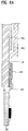
- FIG. 8A is a sectional view taken along the line C-C' of FIG. 2 , illustrating the display panel 100 and the driver circuit unit 140 installed to the display panel 100 according to one embodiment.
- FIG. 8B is a plan view illustrating a part of the rear surface of the transparent board 101 according to the embodiment.
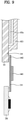
- FIG. 9 is a sectional view taken along the line C-C' of FIG. 2 , illustrating the display panel 100 and the driver circuit unit 140 according to another embodiment.
- the driver circuit unit 140 may include driver ICs 1401 and conductive lines 1402 as described above.
- the driver ICs 1401 may be formed on the transparent board 101 or the rear board 102 so as to overlap the light shielding portion 110 of the transparent board 101, and a least some of the conductive lines 1402 may diagonally extend.
- the driver ICs 1401 and the printed circuit board 200 may be connected to each other via the flexible board 210.
- the driver ICs 1401 may be coupled to the rear surface of the transparent board 101 so as to overlap the light shielding portion 110.
- the encapsulation board 1021 may be bonded to the transparent board 101 at a position inside the light shielding portion 101, and the OLED layer 103a may be located between the encapsulation board 1021 and the transparent board 101.
- the conductive lines 1402 are formed on the rear surface of the transparent board 101 as illustrated in FIG. 8B , at least some of the conductive lines 1402 may diagonally extend.
- the conductive lines 1402 are desirably spaced apart from one another throughout the image display area (10, see FIG. 1 ).
- the driver ICs 1401 cannot be formed in a region of the light shielding portion 110 where the light transmitting portion 120 is located, as illustrated in FIG. 8B . Therefore, the driver ICs 1401 may be arranged at both sides of the light shielding portion 110, and the conductive lines 1402 are patterned such that some of the conductive lines 1402 diagonally extend from the driver ICs 1410 as illustrated in FIG. 8B , so as to transmit a driving signal even to the OLED layer 103a provided immediately inside the light transmitting portion 120.
- the driver IC 1401 may be mounted on the flexible board 210 that connects the driver circuit unit 140 and the printed circuit board 200 to each other, and the conductive line 1402 may be formed on the transparent board 101 or the rear board 102 so as to overlap the light shielding portion 110 of the transparent board 101.
- one end of the driver IC 1401 may be bonded to the rear surface of the transparent board 101 and the other end of the driver IC 1401 may be mounted on the flexible board 210 that is connected to the printed circuit board 200.
- the conductive line 1402 may be provided on the light shielding portion 110 formed at the rear surface of the transparent board 101, and one end of the flexible board 210 may overlap the light shielding portion 110 of the transparent board 101 and may be bonded to the rear surface of the transparent board 101 via a pad electrode.
- the pad electrode may be used to electrically connect the flexible board 210 and the driver IC 1401 to each other, so as to transmit a driving signal to the conductive line 1402.
- FIGS. 10A to 10C are graphs illustrating brightness of the logo displayed by the logo module, respectively, when the display device is in a power-off state, when the display device is changed to a power-on state, and when the display device is changed to a power-off state.
- the controller may control the logo module to display a logo having a first brightness and a first color when power is not applied to the display panel.
- the logo module may be controlled to display a logo having a predetermined color and a predetermined brightness.
- the display device may display the logo through the light transmitting portion even in a standby state of the display device, which enables continuous display of the logo.
- the controller may control the logo module to display the logo such that the logo flickers preset times at a second brightness different from the first brightness.
- the second brightness is greater than the first brightness.
- the controller may control the logo module such that the brightness of the logo displayed by the logo module is gradually increased to the second brightness. Also, the controller may control the logo module such that the logo flickers preset times for a predetermined time. For example, as illustrated in FIG. 10B , the logo module may be controlled such that the logo to flickers three times for 6 seconds as illustrated in FIG. 10B .
- the controller may control the logo module such that a logo, having a second color different from the first color, flickers preset numbers.
- Flickering of the logo is realized by flickering of the logo module, and the user will appreciate from the logo that an instruction to turn on the display device has been input.
- the controller may control the logo module such that the light source of the logo module is turned off, such that the logo is displayed at a third brightness different from the first brightness, or such that the logo having a third color different from the first color is displayed.
- the third brightness may be less than the first brightness and the second brightness as described above.
- the third color may be darker than the first color and the second color as described above.
- the display panel displays an image while power is applied thereto.
- the logo module may not emit light while the display panel displays an image, or the brightness of the logo may be reduced, or a darker color of logo may be displayed in a standby state of the display device.
- the controller may control the logo module such that the light source of the logo module is turned off after completion of the flickering operation, or such that the logo having the third brightness or the third color is displayed.
- the controller may control the logo module such that a logo having a fourth brightness different from the first brightness is displayed.
- the fourth brightness may be greater than the first brightness and less than the second brightness.
- the control signal may be an instruction signal to change the volume of sound output from the display device or to change a channel output from the display device.
- the external controller may be a remote controller or a mobile terminal to generate the control signal.
- the remote controller or the mobile terminal may transmit the control signal to the display device when manipulated by the user. Alternatively, the control signal may be received as the display device is directly manipulated.
- the controller may control the logo module upon receiving the control signal such that the logo having the fourth brightness is displayed.
- the controller may control the logo module such that the logo is displayed at the fourth brightness for a predetermined time. Thereby, the logo may be more brightly viewed by the user of the display device, and consequently the user may visually recognize input of the control signal via the logo.
- the controller may control the logo module upon receiving an external control signal to stop display of the logo.
- the controller may control the logo module such that the logo having a fourth color different from the first color is displayed upon receiving an external control signal.
- the fourth color may be different from the second color or the third color.
- the controller may control the logo module to stop display of the logo for a preset time upon change to apply no power to the display panel.
- the controller may control the logo module such that the logo modules does not temporarily display the logo. After stopping the logo module for a predetermined time, the controller may control the logo module such that the logo module displays the logo having the first brightness when the display device returns to a standby state. While driving of the logo module stops, the logo module does not irradiate light to the logo, and the user may visually check the logo that an instruction to turn off the display device has been received.
- a bezel frame which has conventionally been provided at a front surface of a display device, even while displaying a logo on the front surface of the display device, which may minimize a bezel portion throughout the edge of the display device.
- a manufacturer of the display device and to provide the same size display device with a greater display area, which may advantageously enhance the degree of freedom in terms of design.
Landscapes
- Engineering & Computer Science (AREA)
- Theoretical Computer Science (AREA)
- Physics & Mathematics (AREA)
- General Physics & Mathematics (AREA)
- General Engineering & Computer Science (AREA)
- Computer Hardware Design (AREA)
- Microelectronics & Electronic Packaging (AREA)
- Human Computer Interaction (AREA)
- Optics & Photonics (AREA)
- Devices For Indicating Variable Information By Combining Individual Elements (AREA)
- Electroluminescent Light Sources (AREA)
- Illuminated Signs And Luminous Advertising (AREA)
Description
- The present invention relates to a display device, which minimizes the thickness of a bezel portion using a display panel with an integrated logo.
- A display device refers to a device that displays an input image signal. The concept of a display device includes a monitor that displays an image received from a computer, a television that displays an image and sound transmitted from a broadcasting station, and all other devices that display an image input from the outside.
- In recent years, a Liquid Crystal Display (LCD) panel, an Organic Light Emitting Diode (OLED) panel, and so on are a focus of attention as a flat panel type display module to realize a high-resolution large display device. In general, a display device includes a display panel to form an image, a Printed Circuit Board (PCB) to control the image of the display panel and control sound and communication, a front bezel frame to surround a front rim of the display panel, and a rear cover to cover the rear side of the display panel.
- In such a display device, design factors and user convenience have recently been emphasized to improve aesthetics as well as a basic image display function according to the trend of a greater size, slimness and higher quality. In one example, efforts to develop a borderless display device have continued, in which the entire display device is reminiscent of a single large and black glass panel or frame owing to elimination of a boundary between a screen (display area) and a bezel portion (non-display area) by omitting the front bezel frame of the display device.
- Meanwhile, manufacturers of display devices tend to mount their logo on a front surface of a display device, in order to improve display device brand recognition. The logo must have a predetermined size or more to achieve visual differentiation.
- Conventionally, to install the aforementioned logo, it is essential that the display device be provided at more than one end thereof with the front bezel frame. As a result, the aforementioned borderless display device still faces technical challenges.
- Document
US 7,298,076 B2 may be construed to disclose a bezel-less display that includes an electronic display device and a cover. The electronic display device has an image-displaying portion and another portion adjacent to the image-displaying portion along at least one side. The cover is positioned adjacent to the electronic display device and includes a first portion positioned adjacent to the image-displaying portion of the display device and a second portion positioned adjacent to the other portion of the display device. The optical properties of the first and second portions of the cover are selected to present an appearance of a uniform cover without a bezel when the display device is not displaying an image. The optical properties of the first portion are also selected to transmit images displayed on the image-displaying portion. Preferably, the optical properties of the second portion are selected to mask the other portion of the display device. A secondary display device may also be provided that presents an image, such as a logo, independently of whether the other or main electronic display device is displaying an image. - Document
US 2012/106063 A1 may be construed to disclose an electronic device having a display. Inactive portions of the display such as peripheral portions of the display may be masked using an opaque masking layer. An opening may be provided in the opaque masking layer to allow light to pass. For example, a logo may be viewed through an opening in the opaque masking layer and a camera may receive light through an opening in the opaque masking layer. The display may include upper and lower polarizers, a color filter layer, and a thin-film transistor layer. The opaque masking layer may be formed on the upper polarizer, may be interposed between the upper polarizer and the color filter layer, or may be interposed between the color filter layer and the thin-film transistor layer. The upper polarizer may have unpolarized windows for cameras, logos, or other internal structures. - Accordingly, the present invention is directed to a display device having a display panel with an integrated logo that substantially obviates one or more problems due to limitations and disadvantages of the related art.
- An object of the present invention is to provide a display device, which is capable of displaying a logo on a front surface thereof even while minimizing a bezel portion through omission of a front bezel frame that has conventionally been required to install a logo.
- Additional advantages, objects, and features of the invention will be set forth in part in the description which follows and in part will become apparent to those having ordinary skill in the art upon examination of the following or may be learned from practice of the invention. The objectives and other advantages of the invention may be realized and attained by the structure particularly pointed out in the written description and claims hereof as well as the appended drawings.
- According to the disclosure, there is provided an apparatus according to the independent claim. Developments are set forth in the dependent claims.
- A display device includes a display panel including an image display area for formation of an image and a non-display area formed around the image display area, a driver circuit unit configured to feed a driving signal for formation of the image to the display panel, and a controller configured to control the display panel and the driver circuit unit, wherein the display panel includes a transparent board including a light shielding portion formed along an edge thereof to define the non-display area by blocking light, and a light transmitting portion formed by removing a part of the light shielding portion, a rear board placed to face the transparent board, and a logo module placed on a rear surface of the transparent board so as to overlap the light transmitting portion, the logo module outwardly displaying a logo through the light transmitting portion, and wherein at least a part of the driver circuit unit is formed on the transparent board or the rear board so as to overlap the light shielding portion.
- The logo module includes a light-transmitting diffusion sheet placed at the rear side of the light transmitting portion, a semi-transparent reflective sheet placed at the rear side of the diffusion sheet, and a light source placed at the rear side of the reflective sheet, to introduce light into the reflective sheet.
- Colored light-transmitting ink is applied to the light transmitting portion.
- The display panel further includes an Organic Light Emitting Diode (OLED) layer provided in the image display area between the transparent board and the rear board, the OLED layer serving to emit light, the rear board preferably is bonded to the transparent board so as to seal the OLED layer to the transparent board, the rear board preferably is an encapsulation board having an inwardly indented recess corresponding to the light transmitting portion, and the logo module preferably is located in the recess.
- The display panel preferably further includes a sealing portion to seal a space between the transparent board and the rear board, and a liquid crystal layer placed inside the sealing portion in the space between the transparent board and the rear board, and the light transmitting portion of the transparent board and the logo module preferably is arranged at the outside of the sealing portion.
- The display panel preferably further includes a light-leakage prevention structure configured to surround at least a part of the periphery of the logo module and serving to block light emitted from the logo module for display of the logo.
- The driver circuit unit preferably includes a driver Integrated Chip (IC) formed on the transparent board or the rear board so as to overlap the light shielding portion and serving to generate the driving signal as an electric signal, and a conductive line diagonally extending from the driver IC to transmit the electric signal.
- The display device preferably further includes a printed circuit board provided with the controller, and a flexible board having one end connected to the printed circuit board and the other end connected to the driver circuit unit so as to electrically connect the printed circuit board and the driver circuit unit to each other.
- The flexible board preferably is a Tape Carrier Package (TCP) or a Flexible Printed Circuit Board (FPCB).
- The printed circuit board preferably is placed on a rear surface of the rear board.
- The driver circuit unit preferably includes a driver IC to generate the driving signal as an electric signal and a conductive line to transmit the electric signal, the driver IC preferably is mounted on the flexible board. The conductive line preferably is formed on the transparent board or the rear board so as to overlap the light shielding portion.
- The controller controls the logo module to display the logo having a first brightness and a first color when power is not applied to the display panel.
- The controller controls the logo module to display the logo such that the logo having a second brightness different from the first brightness flickers preset times, or such that the logo having a second color different from the first color flickers preset times, upon change to apply power to the display panel for display of the image.
- The controller preferably controls the logo module to display the logo such that a light source of the logo module is turned off, such that the logo having a third brightness different from the first brightness is displayed, or such that the logo having a third color different from the first color is displayed, while the display panel displays the image.
- The controller preferably controls the logo module to display the logo such that a light source of the logo module is turned off, such that the logo having a fourth brightness different from the first brightness is displayed, or such that the logo having a fourth color different from the first color is displayed, when a control signal is input from an external controller.
- It is to be understood that both the foregoing general description and the following detailed description of the present invention are exemplary and explanatory and are intended to provide further explanation of the invention as claimed.
- The accompanying drawings, which are included to provide a further understanding of the invention and are incorporated in and constitute a part of this application, illustrate embodiment(s) of the invention and together with the description serve to explain the principle of the invention. In the drawings:
-
FIG. 1 is a front perspective view illustrating a display device according to an embodiment of the present invention; -
FIG. 2 is an exploded perspective view illustrating a separated state of a power supply unit, a main control module, and a rear cover included in the display device according to the embodiment ofFIG. 1 ; -
FIG. 3 is an exploded perspective view illustrating a separated state of a logo module and a rear board of a display panel according to the embodiment ofFIG. 2 ; -
FIG. 4 is an exploded perspective view of the logo module included in the display device according to the embodiment of the present invention; -
FIG. 5 is a sectional view taken along the line B-B' ofFIG. 2 , illustrating the display panel according to one embodiment; -
FIG. 6 is a sectional view taken along the line B-B' ofFIG. 2 , illustrating the display panel according to another embodiment; -
FIG. 7 is a partial exploded perspective view illustrating a display device including a light-leakage prevention structure according to another embodiment of the present invention; -
FIG. 8A is a sectional view taken along the line C-C' ofFIG. 2 , illustrating a display panel and a driver circuit unit according to one embodiment; -
FIG. 8B is a partial rear view illustrating a transparent board of the display panel according to the embodiment ofFIG. 8A ; -
FIG. 9 is a sectional view taken along the line C-C' ofFIG. 2 , illustrating a display panel and a driver circuit unit according to another embodiment; and -
FIGS. 10A to 10C are graphs illustrating brightness of a logo displayed by the logo module, respectively, when the display device is in a power-off state, when the display device is changed to a power-on state, and when the display device is changed to a power-off state. - Hereinafter, exemplary embodiments of the present invention will be described in detail with reference to the accompanying drawings. The terms or words used in the specification and claims of the present invention are not interpreted using typical or dictionary limited meanings, and are constructed as meanings and concepts conforming to the technical sprit of the present invention based on the principle that the inventors can appropriately define the concepts of the terms to explain the present invention in the best manner.
- Accordingly, it is to be understood that the detailed description, which will be disclosed along with the accompanying drawings, is intended to describe the exemplary embodiments of the present invention and is not intended to represent all technical ideas of the present invention.
- The terms used in the present invention may be interpreted based on the following references, and even terms not described in the present invention may be interpreted based on the following references. Coding may be interpreted as encoding or decoding as occasion demands, and information is the term including all of values, parameters, coefficients, elements, and the like and may be interpreted differently as occasion demands, and therefore the present invention is not limited thereto. With respect to constituent elements used in the following description, suffixes "module" and "unit" are given or mingled with each other only in consideration of ease in the preparation of the specification, and do not have or serve as different meanings. 'Unit' is used to refer to a basic unit of image processing or a particular position of an image, and may be used along with terms, such as 'block', 'partition', 'region', or the like as occasion demands.
- Hereinafter, a display device according to several embodiments of the present invention will be described with reference to
FIGS. 1 to 9 . -
FIG. 1 is a front perspective view illustrating adisplay device 1 according to an embodiment of the present invention.FIG. 2 is a rear exploded perspective view illustrating a separated state of adisplay panel 100 and arear cover 40 included in the display device according to the embodiment ofFIG. 1 . Also,FIG. 3 is a rear exploded perspective view illustrating a separated state of atransparent board 101, alogo module 130, and arear board 102 constituting thedisplay panel 100 according to the embodiment ofFIG. 2 . - As illustrated in
FIG. 1 , the display device of the present embodiment may realize a borderless display device. In the borderless display device, a front bezel frame that has conventionally been provided at a front rim of thedisplay panel 100 is omitted, and a bezel portion that is anon-display area 20 of a screen may be directly realized from thedisplay panel 100. As a result, when viewing the display device from the front side, only a small-thickness frame surrounding the periphery of thedisplay panel 100 is seen, which may allow the display device to be seen as being constructed only by thedisplay panel 100. - In this case, as illustrated in
FIG. 1 , alogo 30 of a manufacturer is provided in thenon-display area 20 of thedisplay panel 100. Aesthetic functional effects of the logo may be improved with illumination of thelogo 30. To this end, alogo module 130 may be provided to display the logo. Thelogo module 130 is integrally formed with thedisplay panel 100. - The display device of the present invention as described above includes the
display panel 100 with theintegrated logo module 130 as illustrated inFIG. 2 , adriver circuit unit 140, and a controller. - Referring to
FIG. 2 , the display device may further include therear cover 40 configured to cover a rear surface of thedisplay panel 100. Additionally, if necessary, a transparent protective glass (not shown) to protect thedisplay panel 100 may be provided at a front surface of thedisplay panel 100. - The display device may further include a
main control module 50 and apower supply unit 60. Themain control module 50 may control general operations of the display device, and may include a printed circuit board. As occasion demands, themain control module 50 may include a Timing Controller (TCON) board, or may include a System On Chip (SOC). Additionally, themain control module 50 may include an infrared (IR) receiver to receive a control signal from an external controller. The external controller may be a remote controller or other mobile terminals, and may perform infrared communication with themain control module 50. - The
power supply unit 60 serves to apply power, supplied from an external source, to themain control module 50 under the control of a user. - As illustrated in
FIG. 2 , more specifically, themain control module 50 may be connected to a printedcircuit board 200 that is in turn electrically connected to thedriver circuit unit 140, and may also be connected to thelogo module 130, thereby controlling the printedcircuit board 200 and thelogo module 130. To this end, at least some of a variety of electronic elements constituting the controller of the display device according to the present invention may be mounted on themain control module 50. - In one example, the printed
circuit board 200 may transmit a driving signal to thedriver circuit unit 140 under the control of themain control module 50, and consequently may control output of an image from thedisplay panel 100. Themain control module 50 and the printedcircuit board 200 may be electrically connected to each other via a flexible board, such as a Flexible Printed Circuit Board (FPCB). - The
main control module 50 may transmit power, applied from thepower supply unit 60, to thedriver circuit unit 140 and thelogo module 130. Themain control module 50 may actuate thedisplay panel 100 and thelogo module 130 respectively by transmitting power to thedriver circuit unit 140 and thelogo module 130. - The front surface of the
display panel 100, as illustrated inFIG. 1 , consists of animage display area 10 in which an image is formed, and thenon-display area 20 provided around theimage display area 10. Thedisplay panel 100 may include at least one selected from among a Liquid Crystal Display (LCD) panel, a Thin Film Transistor Liquid Crystal Display (TFT LCD) panel, an Organic Light Emitting Diode (OLED) panel, a flexible display panel, and a 3-Dimentional (3D) display panel. - The
driver circuit unit 140 feeds a driving signal to thedisplay panel 100, to form an image in theimage display area 10. Thedriver circuit unit 140 may consist of various electronic elements and lead wires to feed electric signals generated from the electronic elements to thedisplay panel 100. At least some of the constituent elements of thedriver circuit unit 140 may be arranged in thenon-display area 20 of thedisplay panel 100. The controller controls both thedisplay panel 100 and thedriver circuit unit 140. - According to an embodiment, the
driver circuit unit 140 may include driver Integrated Chips (IC) and conductive lines. The driver ICs generate electric driving signals to form an image under the control of the controller, and the conductive lines extend from the driver ICs for transmission of the electric signals. - The driver ICs may take the form of transistors, and may include a plurality of data source driver ICs and a plurality of scan driver ICs. Arranging the driver ICs constituting the
driver circuit unit 140 on a board may mean that the conductive lines, i.e. circuit elements required to drive each driver IC, to be directly patterned on the corresponding board via a semiconductor manufacturing process. - The conductive lines may be formed of a metal and may be directly patterned on the corresponding board. The conductive lines may electrically connect the driver ICs and image forming devices (e.g., organic light emitting diodes, and liquid crystal devices) to each other. The conductive lines may transmit electric signals to the image forming devices, thereby feeding data signals and scan signals to the devices, so as to drive the devices.
- As illustrated in
FIG. 2 , more specifically, thedisplay panel 100 consists of thetransparent board 101, therear board 102, and thelogo module 130. - The
transparent board 101 defines the front surface of thedisplay panel 100. According to an embodiment, thetransparent board 101 may be formed of glass. Alternatively, thetransparent board 101 may be a plastic board formed of transparent synthetic resin. Alternatively, thetransparent board 101 may be formed of a film material. The material and shape of thetransparent board 101 are not limited thereto, and other light transmittable plate-shaped members may be used to form thetransparent board 101. - An electrode, to which voltage is applied to form an image on the
display panel 100, may be formed at an inner surface of thetransparent board 101. When the electrode is formed at thetransparent board 101, the electrode may be a transparent electrode. As occasion demands, thetransparent board 101 may be provided with a Thin Film Transistor (TFT) array. - Referring to
FIG. 3 , thetransparent board 101 may include alight shielding portion 110 and alight transmitting portion 120. Thelight shielding portion 110 may be provided on a front surface or a rear surface of thetransparent board 101 along the edge of thetransparent board 101. - The
light shielding portion 110 may be formed of an opaque material to shield light. Thelight shielding portion 110 configured to shield light defines thenon-display area 20 in which an image is not formed even during driving of thedisplay panel 100. Thelight shielding portion 110 may be obtained by printing a panel line on the rim of one surface of thetransparent board 101, or may be obtained by attaching an opaque black tape to the rim of one surface of thetransparent board 101. InFIG. 3 , an embodiment in which thelight shielding portion 110 is formed at a rear surface of thetransparent board 101 is illustrated. - The
light transmitting portion 120 is formed by removing a part of thelight shielding portion 110. That is, a part of the rim of thetransparent board 101 may be not provided with thelight shielding portion 110 such that only thetransparent board 101 or any other light transmitting member remains. For example, if thelight shielding portion 110 is formed by printing a panel line on one surface of thetransparent board 101, a part of thelight shielding portion 110 may not be subjected to printing, and the resulting non-printed portion may define thelight transmitting portion 120. Thelight transmitting portion 120 transmits light, which allows the logo, displayed by thelogo module 130, to be visible from the outside of thedisplay panel 100. - According to an embodiment, the
light transmitting portion 120 may have a particular pattern. In this case, the particular pattern may form a logo of a manufacturer. According to the present embodiment, even if thelogo module 130 simply functions to emit light, the logo may be displayed as the light emitted from thelogo module 130 passes through thelight transmitting portion 120 having a particular pattern. That is, the pattern of the logo may be determined by the pattern of thelight transmitting portion 120. InFIG. 2 , an embodiment is illustrated in which thelight transmitting portion 120 having a particular pattern is located at a lower end of thelight shielding portion 110 that is formed along the rim of thetransparent board 101. - According to another embodiment, the
logo module 130 may be configured to irradiate light having a particular pattern. In one example, a light source included in thelogo module 130 may be fabricated to have a particular shape, or LED devices constituting the light source may be arranged to yield a particular shape. In particular, if the light source is formed of OLED layers, the OLED layers may have a particular pattern. - In the present embodiment, the
light transmitting portion 120 needs not have a particular pattern. For example, thelight transmitting portion 120 may be obtained by simply removing a rectangular part of thelight shielding portion 110. In this case, the shape of the logo may be defined by the light source of thelogo module 130, and thelight transmitting portion 120 simply functions to transmit light emitted from the light source of thelogo module 130 having a particular shape to the outside of thedisplay panel 100. - According to another embodiment, a light transmitting ink having a particular color may be applied to the
light transmitting portion 120. For example, the light transmitting ink may be semi-transparent white or red ink. Since the light transmitting ink is applied to thelight transmitting portion 120, the logo may emit a particular color of light or various colors of light even when thelogo module 130 is configured only to emit white light, which enables representation of various designs of logos. - The
rear board 102 is placed on the rear surface of thetransparent board 101 such that therear board 102 and thetransparent board 101 face each other. Similarly, therear board 102 may be provided with an electrode to form an image on thedisplay panel 100, or may be provided with a TFT array, as occasion demands. If thedisplay panel 100 is anLCD panel 100, therear board 102 and the electrode formed at therear board 102 may be formed of a light transmitting material, and a backlight unit may further be provided on a rear surface of therear board 102. - As illustrated in
FIG. 2 , thelogo module 130 is placed on the rear surface of thetransparent board 101 so as to overlap thelight transmitting portion 120. Thelogo module 130 is configured to display the logo when voltage is applied thereto, and the logo displayed by thelogo module 130 is outwardly displayed through thelight transmitting portion 120 of thetransparent board 101. Thelogo module 130 is located at the rear side of thelight transmitting portion 120. Thelogo module 130 may be coupled to the rear surface of thetransparent board 101 so as to overlap thelight transmitting portion 120. The coupling may be accomplished via bonding. - The
logo module 130 may be located at the rear side of thetransparent board 101 so as to be placed in the same plane as therear board 102. Alternatively, thelogo module 130 may be interposed between thetransparent board 101 and therear board 102. In the former case, thelogo module 130 may be located at a position around therear board 102, or may overlap therear board 102. If thelogo module 130 and therear board 102 overlap each other in the same plane, therear board 102 may have a hole or recess into which thelogo module 130 is inserted. -
FIG. 4 is an exploded perspective view illustrating an embodiment of thelogo module 130.FIG. 4 is an enlarged view of the portion A ofFIG. 2 , illustrating the shapes of thelight shielding portion 110, thelight transmitting portion 120, and thelogo module 130 according to the embodiment. As illustrated inFIG. 4 , thelogo module 130 according to the embodiment may consist of adiffusion sheet 1301, areflective sheet 1302, and alight source 1303. - The
light source 1303 is operated to emit light. Thelight source 1303 may be formed of LED devices or OLED layers. Thelight source 1303, as illustrated inFIG. 4 , may be mounted on a small auxiliary printed circuit board placed at the rear side of thereflective sheet 1302. Thelight source 1303 may be controlled by the auxiliary printed circuit board so as to introduce light into thereflective sheet 1302. - The
reflective sheet 1302 is placed at the rear side of thediffusion sheet 1301 and is formed of a semi-transparent material. If light emitted from thelight source 1303 is introduced into thereflective sheet 1302, at least a part of the light emitted from thelight source 1303 may pass through the semi-transparentreflective sheet 1302. Thereflective sheet 1302 is placed at the rear side of thediffusion sheet 1301. When the light passes through thereflective sheet 1302, the light may be reflected by thereflective sheet 1302 to thereby be introduced into thediffusion sheet 1301. Thereflective sheet 1302 may have various degrees of transparency, and may be formed by depositing a reflective material having a preset transparency on a transparent sheet. - The
diffusion sheet 1301 may be placed at the rear side of the transmittingportion 120 formed at thetransparent board 101, and may be formed of a transparent material. Thediffusion sheet 1301 may uniformly diffuse light reflected from thereflective sheet 1302 to the entire region of thediffusion sheet 1301. As illustrated inFIG. 4 , thediffusion sheet 1301 may be provided with convex and concave portions to effectively diffuse light. The size of thediffusion sheet 1301 may be greater than an outer boundary of thelight transmitting portion 120. - As the above described
logo module 130 is placed on the rear surface of thelight transmitting portion 120, the logo displayed by thelogo module 130 may be outwardly displayed on thedisplay panel 100 through thelight transmitting portion 120. Since thelight shielding portion 110 is provided around thelight transmitting portion 120, it may appear that light is directed only through the particular pattern of thelight transmitting portion 120 when thelogo module 130 is operated to display the logo, which may realize a light emitting logo. Alternatively, thelogo module 130 may have a self-illuminating function to yield a particular pattern of light emitting logo. - Referring again to
FIGS. 2 and3 , at least a part of thedriver circuit unit 140 included in the display device is formed in thenon-display area 20 of thedisplay panel 100. More specifically, a region of thetransparent board 101 or of therear board 102 where the conductive lines (data lines and scan lines) of thedriver circuit unit 140 are located may overlap thelight shielding portion 110 formed at thetransparent board 101. InFIG. 3 , an embodiment is illustrated, in which thedriver circuit unit 140 overlaps thelight shielding portion 110 on the rear surface of thetransparent board 101. Alternatively, thedriver circuit unit 140 may overlap thelight shielding portion 110 on the front surface of therear board 102. - As illustrated in
FIG. 3 , at least a part of thedriver circuit unit 140 may be located on thelight shielding portion 110 formed at the rim of thetransparent board 101. Here, both thedriver circuit unit 140 and thelight transmitting portion 120 may be formed at the same end of thelight shielding portion 110. That is, thelight shielding portion 110 and thedriver circuit unit 140 may be arranged in a line along one end of thetransparent board 101. In this case, thedriver circuit unit 140 may be provided at one side or either side of thelight transmitting portion 120. When both thelight transmitting portion 120 and thedriver circuit unit 140 are located on the lower end of thetransparent board 101 as illustrated inFIG. 3 , it is possible to minimize thenon-display area 20 of thedisplay panel 100. - To drive the
display panel 100, it is important that any one of thetransparent board 101 or therear board 102 be provided with thedriver circuit unit 140. Also, to realize vivid image display, it is desirable to position thedriver circuit unit 140 in thenon-display area 20 of thedisplay panel 100. That is, it is desirable to provide thenon-display area 20 on at least one end of thedisplay panel 100, in order to hide thedriver circuit unit 140. As a result of locating thelight transmitting portion 120 and thelogo module 130 in thenon-display area 20 that is formed to hide thedriver circuit unit 140, it is possible to omit an additional bezel portion or a conventional front bezel frame that is required to mount the logo. As such, thedisplay panel 100 may have the integrated logo, which may minimize the bezel portion of thedisplay panel 100. -
FIG. 5 is a sectional view taken along the line B-B' ofFIG. 2 , illustrating thedisplay panel 100 according to one embodiment, andFIG. 6 is a sectional view taken along the line B-B' ofFIG. 2 , illustrating thedisplay panel 100 according to another embodiment. - According to one embodiment, the
display panel 100 included in the display device of the present invention may be an OLED panel. In this case, as illustrated inFIG. 5 , thedisplay panel 100 may further include anOLED layer 103a included in the image display area (10, seeFIG. 1 ) between thetransparent board 101 and arear board 1021. TheOLED layer 103a may form an image via light emission when power is applied thereto. - The
rear board 1021 of thedisplay panel 100 may be an encapsulation board bonded to thetransparent board 101 so as to seal theOLED layer 103a to thetransparent board 101. Theencapsulation board 1021 may be formed of a metal. Theencapsulation board 1021 may cover theOLED layer 103a to prevent oxidation or deterioration of theOLED layer 103a due to moisture and air. - At least a part of a bonding region of the
encapsulation board 1021 with respect to thetransparent board 101 may overlap thelight shielding portion 110 of thetransparent board 101. In this case, to provide a space for installation of thelogo module 130 at the rear side of thetransparent board 101, a recess (seeFIG. 3 ) may be inwardly indented in one end of theencapsulation board 1021 at a position corresponding to thelight transmitting portion 120 of thetransparent board 101. That is, the recess may be formed by removing a partial region of one end of theencapsulation board 1021 facing thelight transmitting portion 120. - When the recess is formed in the
encapsulation board 1021 as described above, thelogo module 130 may be accommodated in the recess, and thereafter theencapsulation board 1021 may be bonded to thetransparent board 101 so as to surround thelogo module 130 accommodated in the recess. - More specifically, as illustrated in
FIG. 5 , thelogo module 130 may be coupled to the rear surface of thetransparent board 101 so as to overlap thelight transmitting portion 120 within thenon-display area 20 defined by thelight shielding portion 110. The logo displayed by thelogo module 130 is outwardly displayed through thelight transmitting portion 120 of thetransparent board 101. The recess of theencapsulation board 1021 may be bonded to thetransparent board 101 at a position inside thelogo module 130, and theOLED layer 103a may be interposed between theencapsulation board 1021 and thetransparent board 101. - In the case of the OLED panel as described above, the
logo module 130 is coupled to the rear surface of thetransparent board 101 and is located at a position around theencapsulation board 1021 that encapsulates theOLED layer 103a. Accordingly, despite the fact that thedisplay panel 100 contains theintegrated logo module 130, it is possible to ensure normal operation of theOLED layer 103a as well as independent operation of theOLED layer 103a and thelogo module 130. - According to another embodiment, the
display panel 100 included in the display device of the present invention may be an LCD panel. In this case, as illustrated inFIG. 6 , thedisplay panel 100 may further include a sealingportion 104 to seal a space between thetransparent board 101 and therear board 102, and a liquid crystal layer 130b placed inside the sealingportion 104 between thetransparent board 101 and therear board 102. In addition to the liquid crystal layer 103b, theLCD panel 100 may further include a polarizer, a color filter, and a backlight unit. - The liquid crystal layer 130b may be turned on or off on a per pixel basis by a TFT array provided at the
transparent board 101 or therear board 102, and light emitted from the backlight unit may pass through the turned-on pixels so as to form an image. The sealingportion 104 may seal the liquid crystal layer 130b between thetransparent board 101 and therear board 102 such that the liquid crystal layer 103b is accommodated between thetransparent board 101 and therear board 102, thereby protecting the liquid crystal layer 103b from external shock. - In this case, as illustrated in
FIG. 6 , thelight transmitting portion 120 and thelogo module 130 of thetransparent board 101 are located at the outside of the sealingportion 104. According to an embodiment, the sealingportion 104 may be configured to surround one end of thelogo module 130 toward the liquid crystal layer 103b and another end of thelogo module 130 extending perpendicular to the previously described end. As illustrated inFIG. 6 , thelogo module 130 may be coupled to the rear surface of thetransparent board 101 so as to overlap thelight transmitting portion 120 within thenon-display area 20 defined by thelight shielding portion 110. The logo displayed by thelogo module 130 is outwardly displayed through thelight transmitting portion 120 of thetransparent board 101. The sealingportion 104 may be located inside thelogo module 130, and in turn the liquid crystal layer 130b may be located inside the sealingportion 104. - In the
LCD panel 100 of the present embodiment, thelogo module 130 is coupled to the rear surface of thetransparent board 101 and is located at a position around the sealingportion 104 that seals the liquid crystal layer 103b. As a result, despite the fact that thedisplay panel 100 contains theintegrated logo module 130, it is possible to ensure normal operation of the liquid crystal layer 103b as well as independent operation of the liquid crystal layer 130b and thelogo module 130. - As described above, the
display panel 100 with the integrated logo of the present invention may be anLCD panel 100 or an OLED panel. Additionally, thedisplay panel 100 with the integrated logo of the present invention may include various other display panels, such as a TFT LCD panel, a flexible display panel, and the like. In the following description with reference toFIGS. 7 to 9 , for convenience, thedisplay panel 100 with the integrated logo of the present invention is illustrated as the OLED panel illustrated inFIG. 5 . -
FIG. 7 is an enlarged view of the portion A ofFIG. 2 , illustrating an embodiment in which thedisplay panel 100 of the present invention further includes a light-leakage prevention structure 150. - According to an embodiment, the
display panel 100 may further include a light-leakage prevention structure 150. As illustrated inFIG. 7 , the light-leakage prevention structure 150 may be configured to surround at least a part of the periphery of thelogo module 130, and serve to block light emitted from thelogo module 130 to display the logo. To this end, the light-leakage prevention structure 150 may be formed of an opaque material. For example, the light-leakage prevention structure 150 may be formed of opaque silicon. - In one example, as illustrated in
FIG. 7 , thelogo module 130 may be inserted into the recess formed in therear board 102. The light-leakage prevention structure 150 may be provided between thelogo module 130 and the recess of therear board 102. If the light-leakage prevention structure 150 is formed of opaque silicon, the light-leakage prevention structure 150 may be applied to a gap that may be generated between thelogo module 130 and the recess of therear board 102. - The light-
leakage prevention structure 150 may directly block light emitted from thelogo module 130 when displaying the logo, thereby preventing the light from being diffused within thedisplay panel 100. In one example, the light-leakage prevention structure 150 may prevent light emitted from thelogo module 130 from accessing theOLED layer 103a or the liquid crystal layer 103b. In another example, if a backlight unit is provided, it is possible to prevent light emitted from thelogo module 130 from interfering with light emitted from the backlight unit. As a result, it is possible to prevent thelogo module 130 from deteriorating the image display function of thedisplay panel 100. - According to an embodiment, the display device of the present invention may further include the printed
circuit board 200, and aflexible board 210 that connects the printedcircuit board 200 and thedriver circuit unit 140 to each other. The printedcircuit board 200 may include the controller. Specifically, theflexible board 210 may be a Tape Carrier Package (TCP) or an FPCB. One example of the printedcircuit board 200 and theflexible board 210 may be appreciated with reference toFIGS. 2 and3 . - A variety of electronic elements to construct the controller may be mounted on the printed
circuit board 200, and the printedcircuit board 200 may function as a Timing Controller (TCON) board for formation of an image of the display device, as occasion demands. Theflexible board 210 has one end connected to the printedcircuit board 200 and the other end connected to thedriver circuit unit 140, thereby electrically connecting the printedcircuit board 200 and thedriver circuit unit 140 to each other. Theflexible board 210 may transmit a control signal, generated from the printedcircuit board 200, to thedriver circuit unit 140. - Alternatively, the controller may be included in the main control module (50, see
FIG. 2 ), rather than the printedcircuit board 200. In this case, a variety of electronic elements to construct the controller may be provided at themain control module 50. Themain control module 50 may function as a TCON board. Themain control module 50 may be electrically connected to the printedcircuit board 200 to transmit a control signal to the printedcircuit board 200. Also, themain control module 50 may be electrically connected to thelogo module 130 and may transmit a control signal even to thelogo module 130. - Referring to
FIGS. 2 and3 , in a state in which theflexible board 210 physically connects thedriver circuit unit 140 and the printedcircuit board 200 to each other, the printedcircuit board 200 may be placed on a rear surface of therear board 102. Theflexible board 210 may be formed of a flexible material that can freely bend. Through bending of theflexible board 210, the printedcircuit board 200 may be placed on the rear surface of therear board 102. - When the printed
circuit board 200 is placed on the rear surface of therear board 102, the printedcircuit board 200 overlaps thedisplay panel 100. This may minimize the bezel portion of thedisplay panel 100. -
FIG. 8A is a sectional view taken along the line C-C' ofFIG. 2 , illustrating thedisplay panel 100 and thedriver circuit unit 140 installed to thedisplay panel 100 according to one embodiment.FIG. 8B is a plan view illustrating a part of the rear surface of thetransparent board 101 according to the embodiment. Also,FIG. 9 is a sectional view taken along the line C-C' ofFIG. 2 , illustrating thedisplay panel 100 and thedriver circuit unit 140 according to another embodiment. - According to one embodiment, the
driver circuit unit 140 may includedriver ICs 1401 andconductive lines 1402 as described above. In this case, thedriver ICs 1401 may be formed on thetransparent board 101 or therear board 102 so as to overlap thelight shielding portion 110 of thetransparent board 101, and a least some of theconductive lines 1402 may diagonally extend. - In this case, as illustrated in
FIG. 8A , thedriver ICs 1401 and the printedcircuit board 200 may be connected to each other via theflexible board 210. InFIG. 8A , thedriver ICs 1401 may be coupled to the rear surface of thetransparent board 101 so as to overlap thelight shielding portion 110. As described above, theencapsulation board 1021 may be bonded to thetransparent board 101 at a position inside thelight shielding portion 101, and theOLED layer 103a may be located between theencapsulation board 1021 and thetransparent board 101. - In the case in which the
conductive lines 1402 are formed on the rear surface of thetransparent board 101 as illustrated inFIG. 8B , at least some of theconductive lines 1402 may diagonally extend. - To transmit a driving signal to the
entire OLED layer 103a, theconductive lines 1402 are desirably spaced apart from one another throughout the image display area (10, seeFIG. 1 ). In the case in which thelight transmitting portion 120 is formed by removing a part of thelight shielding portion 110 of thetransparent board 101 as described in the embodiment of the present invention, thedriver ICs 1401 cannot be formed in a region of thelight shielding portion 110 where thelight transmitting portion 120 is located, as illustrated inFIG. 8B . Therefore, thedriver ICs 1401 may be arranged at both sides of thelight shielding portion 110, and theconductive lines 1402 are patterned such that some of theconductive lines 1402 diagonally extend from the driver ICs 1410 as illustrated inFIG. 8B , so as to transmit a driving signal even to theOLED layer 103a provided immediately inside thelight transmitting portion 120. - According to another embodiment, as illustrated in
FIG. 9 , thedriver IC 1401 may be mounted on theflexible board 210 that connects thedriver circuit unit 140 and the printedcircuit board 200 to each other, and theconductive line 1402 may be formed on thetransparent board 101 or therear board 102 so as to overlap thelight shielding portion 110 of thetransparent board 101. - As illustrated in
FIG. 9 , one end of thedriver IC 1401 may be bonded to the rear surface of thetransparent board 101 and the other end of thedriver IC 1401 may be mounted on theflexible board 210 that is connected to the printedcircuit board 200. In this case, theconductive line 1402 may be provided on thelight shielding portion 110 formed at the rear surface of thetransparent board 101, and one end of theflexible board 210 may overlap thelight shielding portion 110 of thetransparent board 101 and may be bonded to the rear surface of thetransparent board 101 via a pad electrode. The pad electrode may be used to electrically connect theflexible board 210 and thedriver IC 1401 to each other, so as to transmit a driving signal to theconductive line 1402. - Hereinafter, a control method of the
logo module 130 included in the display device according to an embodiment of the present invention will be described with reference toFIGS. 10A to 10C . -
FIGS. 10A to 10C are graphs illustrating brightness of the logo displayed by the logo module, respectively, when the display device is in a power-off state, when the display device is changed to a power-on state, and when the display device is changed to a power-off state. - According to an embodiment, the controller may control the logo module to display a logo having a first brightness and a first color when power is not applied to the display panel.
- As illustrated in
FIG. 10A , even when the display device does not display an image in a power-off state thereof, the logo module may be controlled to display a logo having a predetermined color and a predetermined brightness. As a result, the display device may display the logo through the light transmitting portion even in a standby state of the display device, which enables continuous display of the logo. - According to another embodiment, upon change to apply power to the display panel in order to display an image, the controller may control the logo module to display the logo such that the logo flickers preset times at a second brightness different from the first brightness. In this case, it is desirable that the second brightness is greater than the first brightness.
- As illustrated in
FIG. 10B , when an instruction to turn on the display device that has been in a power-off state is input to the controller, the controller may control the logo module such that the brightness of the logo displayed by the logo module is gradually increased to the second brightness. Also, the controller may control the logo module such that the logo flickers preset times for a predetermined time. For example, as illustrated inFIG. 10B , the logo module may be controlled such that the logo to flickers three times for 6 seconds as illustrated inFIG. 10B . - Alternatively, upon change to apply power to the display panel, the controller may control the logo module such that a logo, having a second color different from the first color, flickers preset numbers.
- Flickering of the logo is realized by flickering of the logo module, and the user will appreciate from the logo that an instruction to turn on the display device has been input.
- According to another embodiment, while the display panel displays an image, i.e. while the display panel is in a power-on state, the controller may control the logo module such that the light source of the logo module is turned off, such that the logo is displayed at a third brightness different from the first brightness, or such that the logo having a third color different from the first color is displayed. In this case, the third brightness may be less than the first brightness and the second brightness as described above. Also, the third color may be darker than the first color and the second color as described above.
- The display panel displays an image while power is applied thereto. Upon display of the image, if the logo located at the end of the image display area is brightly displayed, the logo may distract the viewer. To prevent this problem, in the present embodiment, the logo module may not emit light while the display panel displays an image, or the brightness of the logo may be reduced, or a darker color of logo may be displayed in a standby state of the display device.
- If the logo is displayed as flickering while power is applied to the display panel as described above, the controller may control the logo module such that the light source of the logo module is turned off after completion of the flickering operation, or such that the logo having the third brightness or the third color is displayed.
- According to another embodiment, if a control signal is input from an external controller, the controller may control the logo module such that a logo having a fourth brightness different from the first brightness is displayed. In this case, the fourth brightness may be greater than the first brightness and less than the second brightness.
- The control signal may be an instruction signal to change the volume of sound output from the display device or to change a channel output from the display device. The external controller may be a remote controller or a mobile terminal to generate the control signal. The remote controller or the mobile terminal may transmit the control signal to the display device when manipulated by the user. Alternatively, the control signal may be received as the display device is directly manipulated.
- Referring to
FIG. 10B , if the control signal is input from the remote controller while the display device is turned on to output an image, the controller may control the logo module upon receiving the control signal such that the logo having the fourth brightness is displayed. According to an embodiment, the controller may control the logo module such that the logo is displayed at the fourth brightness for a predetermined time. Thereby, the logo may be more brightly viewed by the user of the display device, and consequently the user may visually recognize input of the control signal via the logo. - Alternatively, the controller may control the logo module upon receiving an external control signal to stop display of the logo. Alternatively, the controller may control the logo module such that the logo having a fourth color different from the first color is displayed upon receiving an external control signal. The fourth color may be different from the second color or the third color. According to another embodiment, the controller may control the logo module to stop display of the logo for a preset time upon change to apply no power to the display panel.
- Referring to
FIG. 10C , if an instruction to turn off the display device that has been in a power-on state is input, the controller may control the logo module such that the logo modules does not temporarily display the logo. After stopping the logo module for a predetermined time, the controller may control the logo module such that the logo module displays the logo having the first brightness when the display device returns to a standby state. While driving of the logo module stops, the logo module does not irradiate light to the logo, and the user may visually check the logo that an instruction to turn off the display device has been received. - As is apparent from the above description, according to at least one embodiment of the present invention, it is possible to completely omit a bezel frame, which has conventionally been provided at a front surface of a display device, even while displaying a logo on the front surface of the display device, which may minimize a bezel portion throughout the edge of the display device. Thus, it is possible to effectively display a manufacturer of the display device and to provide the same size display device with a greater display area, which may advantageously enhance the degree of freedom in terms of design.
- It will be apparent to those skilled in the art that various modifications and variations can be made in the present invention without departing from the scope of the appended claims. Thus, it is intended that the present invention covers the modifications and variations of this invention provided they come within the scope of the appended claims.
Claims (9)
- A display device comprising:a display panel (100) including an image display area (10) configured to form an image and a non-display area (20) formed around the image display area (10), the display panel (100) including:- a transparent board (101) including a light shielding portion (110) formed along an edge thereof, configured to define the non-display area (20) by blocking light and a light transmitting portion (120) formed at a part of the light shielding portion, wherein colored light-transmitting ink is applied to the light transmitting portion;- an Organic Light Emitting Diode, OLED, layer (103a) or a liquid crystal layer (103b) placed at a rear surface of the transparent board corresponding to the image display area;- a rear board (102) placed to face the transparent board (101); and- a logo module (130) placed at a rear surface of the transparent board (101) so as to overlap the light transmitting portion (120), the logo module (130) being configured to outwardly display a logo (30) through the light transmitting portion (120), the logo module (130) further comprising:-- a light-transmitting diffusion sheet (1301) at a rear side of the light transmitting portion (120) and the light shielding portion;-- a semi-transparent reflective sheet (1302) at a rear side of the diffusion sheet; and-- a light source (1303) at a rear side of the semi-transparent reflective sheet to introduce light into the semi-transparent reflective sheet,--- wherein the semi-transparent reflective sheet is located between the light-transmitting diffusion sheet and the light source such that the light-transmitting diffusion sheet uniformly diffuses light reflected from the semi-transparent reflective sheet to the entire region of the light-transmitting diffusion sheet,--- wherein the light-transmitting diffusion sheet, the semi-transparent reflective sheet and the light source have substantially the same size, and--- wherein the light-transmitting diffusion sheet contacts the light transmitting portion and the light shielding portion;a driver circuit unit (140) configured to feed a driving signal to form the image at the image display area (10), at least a part of the driver circuit unit (140) being formed on one of the transparent board (101) and the rear board (102) so as to overlap the light shielding portion (110); anda controller configured to control the display panel (100) and the driver circuit unit (140),wherein the controller is configured to control the logo module for displaying the logo with a first brightness and a first color when power is not applied to the display panel and for flickering the logo a preset number of times with a second brightness or a second color upon change to apply power to the display panel for display of the image, andwherein the second brightness is different from the first brightness and the second color is different from the first color.
- The display device according to claim 1, wherein the OLED layer is provided between the transparent board (101) and the rear board (102) in the image display area (10), the OLED layer being configured to emit light,
wherein the rear board (102) is bonded to the transparent board (101) so as to seal the OLED layer to the transparent board (101), the rear board (102) being an encapsulation board (1021) having an inwardly indented recess part corresponding to the light transmitting portion (120), and
wherein the logo module (130) is located in the recess part. - The display device according to claim 1, wherein the display panel (100) further includes a sealing portion (104) configured to seal a space between the transparent board (101) and the rear board (102),
wherein the liquid crystal layer is provided between the transparent board (101) and the rear board (102) such that the sealing portion (104) surrounds a perimeter of the liquid crystal layer, and
wherein the light transmitting portion (120) of the transparent board (101) and the logo module (130) are arranged at an outside of the sealing portion (104). - The display device according to claim 1, wherein the display panel (100) further includes a light-leakage prevention structure (150) configured to:- surround at least a part of the periphery of the logo module (130) and- block light emitted from the logo module (130) for display of the logo (30).
- The display device according to claim 1, wherein the driver circuit unit (140) includes:a driver Integrated Chip, IC, (1401) located at one of the transparent board (101) and the rear board (102) so as to overlap the light shielding portion (110), the driver IC (1401) being configured to generate the driving signal as an electric signal; anda conductive line (1402) diagonally extending from the driver IC (1401) and configured to transmit the electric signal.
- The display device according to claim 1, further comprising:a printed circuit board (200) provided with the controller; anda flexible board (210) having one end connected to the printed circuit board (200) and the other end connected to the driver circuit unit (140) so as to electrically connect the printed circuit board (200) to the driver circuit unit (140).
- The display device according to claim 6, wherein the flexible board (210) is one of a tape carrier package and a flexible printed circuit board.
- The display device according to claim 6, wherein the printed circuit board is located at a rear surface of the rear board (102).
- The display device according to claim 6, wherein the driver circuit unit (140) includes a driver integrated chip, IC, (1401) configured to generate the driving signal as an electric signal and a conductive line (1402) configured to transmit the electric signal,
wherein the driver IC (1401) is mounted on the flexible board, and
wherein the conductive line (1402) is formed on one of the transparent board (101) and the rear board (102) so as to overlap the light shielding portion (110).
Applications Claiming Priority (1)
| Application Number | Priority Date | Filing Date | Title |
|---|---|---|---|
| KR1020130014051A KR102037320B1 (en) | 2013-02-07 | 2013-02-07 | Displaying device comprising dispaly panel integrated with logo |
Publications (3)
| Publication Number | Publication Date |
|---|---|
| EP2765475A2 EP2765475A2 (en) | 2014-08-13 |
| EP2765475A3 EP2765475A3 (en) | 2017-04-12 |
| EP2765475B1 true EP2765475B1 (en) | 2021-01-27 |
Family
ID=48949004
Family Applications (1)
| Application Number | Title | Priority Date | Filing Date |
|---|---|---|---|
| EP13003950.6A Active EP2765475B1 (en) | 2013-02-07 | 2013-08-07 | Display device having display panel with integrated logo |
Country Status (4)
| Country | Link |
|---|---|
| US (1) | US9218763B2 (en) |
| EP (1) | EP2765475B1 (en) |
| KR (1) | KR102037320B1 (en) |
| CN (1) | CN103984138B (en) |
Families Citing this family (19)
| Publication number | Priority date | Publication date | Assignee | Title |
|---|---|---|---|---|
| KR101892254B1 (en) * | 2012-05-25 | 2018-08-27 | 삼성전자주식회사 | Display apparatus |
| WO2016077336A2 (en) * | 2014-11-10 | 2016-05-19 | Centifyhealth, Inc. | Interchangeable panel or plate for server case |
| KR101501427B1 (en) * | 2014-11-20 | 2015-03-12 | 주식회사 에스에스뉴테크 | Cover window of mobile device and manufacturing method thereof |
| KR102477954B1 (en) * | 2015-08-12 | 2022-12-16 | 삼성전자주식회사 | Apparatus and method for controlling brightness of light source |
| TWI591401B (en) | 2016-10-21 | 2017-07-11 | 友達光電股份有限公司 | Display device |
| KR102721751B1 (en) * | 2016-12-16 | 2024-10-23 | 엘지디스플레이 주식회사 | Flexible display device |
| KR102562001B1 (en) * | 2017-01-13 | 2023-08-02 | 삼성전자주식회사 | Electronic device with light emitting device |
| WO2018145265A1 (en) * | 2017-02-08 | 2018-08-16 | 深圳迈瑞生物医疗电子股份有限公司 | Ultrasound imaging apparatus |
| CN106918945A (en) * | 2017-03-15 | 2017-07-04 | 惠科股份有限公司 | Display device and display panel thereof |
| US11416082B1 (en) * | 2017-09-05 | 2022-08-16 | Apple Inc. | Input devices with glyphs having a semitransparent mirror layer |
| KR102477040B1 (en) * | 2018-01-04 | 2022-12-14 | 삼성전자주식회사 | Display apparatus and electronic apparatus |
| CN108711381B (en) * | 2018-06-01 | 2020-03-17 | 四川长虹电器股份有限公司 | LOGO indicating lamp structure |
| CN110333622B (en) * | 2019-06-11 | 2021-01-08 | 惠科股份有限公司 | Display panel and display device |
| CN110379831A (en) * | 2019-06-11 | 2019-10-25 | 惠科股份有限公司 | Display panel and display device |
| CN110456551B (en) * | 2019-06-11 | 2021-01-08 | 惠科股份有限公司 | Display panel and display device |
| CN112860126B (en) * | 2021-03-22 | 2024-03-05 | 京东方科技集团股份有限公司 | Display device, touch display panel, touch panel and manufacturing method thereof |
| TWI764794B (en) * | 2021-07-28 | 2022-05-11 | 友達光電股份有限公司 | Display device |
| CN114967201A (en) * | 2022-04-26 | 2022-08-30 | 华映科技(集团)股份有限公司 | An LCD display structure |
| CN117636738A (en) * | 2022-08-15 | 2024-03-01 | 纬联电子科技(中山)有限公司 | Chassis components and displays |
Family Cites Families (15)
| Publication number | Priority date | Publication date | Assignee | Title |
|---|---|---|---|---|
| US5986736A (en) * | 1995-04-26 | 1999-11-16 | Canon Kabushiki Kaisha | Liquid crystal device, image display apparatus and image forming apparatus |
| US6977808B2 (en) * | 1999-05-14 | 2005-12-20 | Apple Computer, Inc. | Display housing for computing device |
| US7766517B2 (en) * | 2001-06-15 | 2010-08-03 | Apple Inc. | Active enclosure for computing device |
| AU2003225641A1 (en) * | 2002-09-03 | 2004-03-29 | Bloomberg Lp | Bezel-less electronic display |
| WO2007034599A1 (en) * | 2005-09-26 | 2007-03-29 | Sharp Kabushiki Kaisha | Display device |
| US7803016B2 (en) * | 2006-06-20 | 2010-09-28 | Belkin International, Inc. | Electronic accessory for an MP3 player, and method of providing the same |
| US7663062B1 (en) * | 2008-07-30 | 2010-02-16 | Himax Technologies Limited | Flexible circuit board |
| KR101511493B1 (en) * | 2008-11-27 | 2015-04-14 | 삼성디스플레이 주식회사 | Liquid crystal display module and display apparatus set having the same, and method of assembling the liquid crystal display module |
| CN102783173B (en) * | 2010-02-26 | 2014-12-17 | 夏普株式会社 | Content reproduction device, television receiver, content reproduction method, content reproduction program, and recording medium |
| US8531130B2 (en) * | 2010-03-31 | 2013-09-10 | Vizio, Inc. | System, method and apparatus for brightness adjusting of an illuminated logo |
| KR101792095B1 (en) * | 2010-10-22 | 2017-11-02 | 삼성디스플레이 주식회사 | Display divce |
| US8467177B2 (en) * | 2010-10-29 | 2013-06-18 | Apple Inc. | Displays with polarizer windows and opaque masking layers for electronic devices |
| US20120182722A1 (en) * | 2011-01-14 | 2012-07-19 | Ming-Yuan Wu | Illuminated vehicle emblem |
| JP5919507B2 (en) * | 2011-09-13 | 2016-05-18 | パナソニックIpマネジメント株式会社 | Electronic device, light emitting unit, and translucent panel |
| US10553002B2 (en) * | 2012-08-31 | 2020-02-04 | Apple, Inc. | Information display using electronic diffusers |
-
2013
- 2013-02-07 KR KR1020130014051A patent/KR102037320B1/en active Active
- 2013-05-21 US US13/899,308 patent/US9218763B2/en active Active
- 2013-08-07 EP EP13003950.6A patent/EP2765475B1/en active Active
- 2013-09-10 CN CN201310409742.5A patent/CN103984138B/en active Active
Non-Patent Citations (1)
| Title |
|---|
| None * |
Also Published As
| Publication number | Publication date |
|---|---|
| EP2765475A3 (en) | 2017-04-12 |
| CN103984138A (en) | 2014-08-13 |
| EP2765475A2 (en) | 2014-08-13 |
| US20140218412A1 (en) | 2014-08-07 |
| CN103984138B (en) | 2017-03-01 |
| US9218763B2 (en) | 2015-12-22 |
| KR102037320B1 (en) | 2019-10-28 |
| KR20140101060A (en) | 2014-08-19 |
Similar Documents
| Publication | Publication Date | Title |
|---|---|---|
| US9218763B2 (en) | Display device having display panel with integrated logo | |
| US11231620B2 (en) | Display apparatus comprising a bracket including a side portion having an outer side surface entirely exposed to form an exterior side surface and a supporting portion extending inwardly from the side portion | |
| US11137645B2 (en) | Electronic apparatus | |
| US10101524B2 (en) | Display apparatus | |
| US9078341B2 (en) | Display device | |
| US10306729B2 (en) | Display with ambient-adaptive backlight color | |
| KR102221154B1 (en) | Display Device | |
| KR102188105B1 (en) | Display apparatus | |
| US9983447B2 (en) | Flat panel display with narrow bezel area | |
| US10467934B2 (en) | Display device | |
| US10598971B2 (en) | Display device | |
| US10965797B2 (en) | Terminal | |
| KR20170047980A (en) | Backlight unit, liquid crystal display device and electronic apparatus comprising the same | |
| US10485106B2 (en) | Structure for connecting printed circuit board and display apparatus having the same | |
| EP3559733B1 (en) | Display apparatus | |
| KR20130126407A (en) | Liquid crystal display device | |
| US10860277B2 (en) | Coupled display device | |
| KR101920760B1 (en) | Liquid crystal display module inculding backlight unit | |
| WO2021012209A1 (en) | Terminal device | |
| KR20180046467A (en) | Back light unit and liquid crystal display device using the same | |
| KR102465447B1 (en) | LED FPCB Tape module and Display device having the same | |
| KR20170127216A (en) | borderless type Liquid Crystal Display device | |
| EP4394492A1 (en) | Display device and light source device thereof | |
| KR20100047590A (en) | Chip on glass type liquid crystal display device | |
| KR102091113B1 (en) | Slim type large area display device |
Legal Events
| Date | Code | Title | Description |
|---|---|---|---|
| PUAI | Public reference made under article 153(3) epc to a published international application that has entered the european phase |
Free format text: ORIGINAL CODE: 0009012 |
|
| 17P | Request for examination filed |
Effective date: 20130807 |
|
| AK | Designated contracting states |
Kind code of ref document: A2 Designated state(s): AL AT BE BG CH CY CZ DE DK EE ES FI FR GB GR HR HU IE IS IT LI LT LU LV MC MK MT NL NO PL PT RO RS SE SI SK SM TR |
|
| AX | Request for extension of the european patent |
Extension state: BA ME |
|
| PUAL | Search report despatched |
Free format text: ORIGINAL CODE: 0009013 |
|
| AK | Designated contracting states |
Kind code of ref document: A3 Designated state(s): AL AT BE BG CH CY CZ DE DK EE ES FI FR GB GR HR HU IE IS IT LI LT LU LV MC MK MT NL NO PL PT RO RS SE SI SK SM TR |
|
| AX | Request for extension of the european patent |
Extension state: BA ME |
|
| RIC1 | Information provided on ipc code assigned before grant |
Ipc: G06F 1/16 20060101AFI20170303BHEP |
|
| STAA | Information on the status of an ep patent application or granted ep patent |
Free format text: STATUS: EXAMINATION IS IN PROGRESS |
|
| 17Q | First examination report despatched |
Effective date: 20191022 |
|
| GRAP | Despatch of communication of intention to grant a patent |
Free format text: ORIGINAL CODE: EPIDOSNIGR1 |
|
| STAA | Information on the status of an ep patent application or granted ep patent |
Free format text: STATUS: GRANT OF PATENT IS INTENDED |
|
| INTG | Intention to grant announced |
Effective date: 20200821 |
|
| GRAS | Grant fee paid |
Free format text: ORIGINAL CODE: EPIDOSNIGR3 |
|
| GRAA | (expected) grant |
Free format text: ORIGINAL CODE: 0009210 |
|
| STAA | Information on the status of an ep patent application or granted ep patent |
Free format text: STATUS: THE PATENT HAS BEEN GRANTED |
|
| RAP1 | Party data changed (applicant data changed or rights of an application transferred) |
Owner name: LG ELECTRONICS, INC. |
|
| RIN1 | Information on inventor provided before grant (corrected) |
Inventor name: HWANGBO, DEUNG Inventor name: KIM, JUNKI |
|
| AK | Designated contracting states |
Kind code of ref document: B1 Designated state(s): AL AT BE BG CH CY CZ DE DK EE ES FI FR GB GR HR HU IE IS IT LI LT LU LV MC MK MT NL NO PL PT RO RS SE SI SK SM TR |
|
| REG | Reference to a national code |
Ref country code: GB Ref legal event code: FG4D |
|
| REG | Reference to a national code |
Ref country code: CH Ref legal event code: EP |
|
| REG | Reference to a national code |
Ref country code: DE Ref legal event code: R082 Ref document number: 602013075462 Country of ref document: DE Representative=s name: WUESTHOFF & WUESTHOFF, PATENTANWAELTE PARTG MB, DE |
|
| REG | Reference to a national code |
Ref country code: AT Ref legal event code: REF Ref document number: 1358954 Country of ref document: AT Kind code of ref document: T Effective date: 20210215 |
|
| REG | Reference to a national code |
Ref country code: IE Ref legal event code: FG4D |
|
| REG | Reference to a national code |
Ref country code: DE Ref legal event code: R096 Ref document number: 602013075462 Country of ref document: DE |
|
| REG | Reference to a national code |
Ref country code: NL Ref legal event code: MP Effective date: 20210127 |
|
| REG | Reference to a national code |
Ref country code: LT Ref legal event code: MG9D |
|
| REG | Reference to a national code |
Ref country code: AT Ref legal event code: MK05 Ref document number: 1358954 Country of ref document: AT Kind code of ref document: T Effective date: 20210127 |
|
| PG25 | Lapsed in a contracting state [announced via postgrant information from national office to epo] |
Ref country code: HR Free format text: LAPSE BECAUSE OF FAILURE TO SUBMIT A TRANSLATION OF THE DESCRIPTION OR TO PAY THE FEE WITHIN THE PRESCRIBED TIME-LIMIT Effective date: 20210127 Ref country code: GR Free format text: LAPSE BECAUSE OF FAILURE TO SUBMIT A TRANSLATION OF THE DESCRIPTION OR TO PAY THE FEE WITHIN THE PRESCRIBED TIME-LIMIT Effective date: 20210428 Ref country code: FI Free format text: LAPSE BECAUSE OF FAILURE TO SUBMIT A TRANSLATION OF THE DESCRIPTION OR TO PAY THE FEE WITHIN THE PRESCRIBED TIME-LIMIT Effective date: 20210127 Ref country code: LT Free format text: LAPSE BECAUSE OF FAILURE TO SUBMIT A TRANSLATION OF THE DESCRIPTION OR TO PAY THE FEE WITHIN THE PRESCRIBED TIME-LIMIT Effective date: 20210127 Ref country code: PT Free format text: LAPSE BECAUSE OF FAILURE TO SUBMIT A TRANSLATION OF THE DESCRIPTION OR TO PAY THE FEE WITHIN THE PRESCRIBED TIME-LIMIT Effective date: 20210527 Ref country code: NO Free format text: LAPSE BECAUSE OF FAILURE TO SUBMIT A TRANSLATION OF THE DESCRIPTION OR TO PAY THE FEE WITHIN THE PRESCRIBED TIME-LIMIT Effective date: 20210427 Ref country code: NL Free format text: LAPSE BECAUSE OF FAILURE TO SUBMIT A TRANSLATION OF THE DESCRIPTION OR TO PAY THE FEE WITHIN THE PRESCRIBED TIME-LIMIT Effective date: 20210127 Ref country code: BG Free format text: LAPSE BECAUSE OF FAILURE TO SUBMIT A TRANSLATION OF THE DESCRIPTION OR TO PAY THE FEE WITHIN THE PRESCRIBED TIME-LIMIT Effective date: 20210427 |
|
| PG25 | Lapsed in a contracting state [announced via postgrant information from national office to epo] |
Ref country code: RS Free format text: LAPSE BECAUSE OF FAILURE TO SUBMIT A TRANSLATION OF THE DESCRIPTION OR TO PAY THE FEE WITHIN THE PRESCRIBED TIME-LIMIT Effective date: 20210127 Ref country code: PL Free format text: LAPSE BECAUSE OF FAILURE TO SUBMIT A TRANSLATION OF THE DESCRIPTION OR TO PAY THE FEE WITHIN THE PRESCRIBED TIME-LIMIT Effective date: 20210127 Ref country code: LV Free format text: LAPSE BECAUSE OF FAILURE TO SUBMIT A TRANSLATION OF THE DESCRIPTION OR TO PAY THE FEE WITHIN THE PRESCRIBED TIME-LIMIT Effective date: 20210127 Ref country code: AT Free format text: LAPSE BECAUSE OF FAILURE TO SUBMIT A TRANSLATION OF THE DESCRIPTION OR TO PAY THE FEE WITHIN THE PRESCRIBED TIME-LIMIT Effective date: 20210127 Ref country code: SE Free format text: LAPSE BECAUSE OF FAILURE TO SUBMIT A TRANSLATION OF THE DESCRIPTION OR TO PAY THE FEE WITHIN THE PRESCRIBED TIME-LIMIT Effective date: 20210127 |
|
| PG25 | Lapsed in a contracting state [announced via postgrant information from national office to epo] |
Ref country code: IS Free format text: LAPSE BECAUSE OF FAILURE TO SUBMIT A TRANSLATION OF THE DESCRIPTION OR TO PAY THE FEE WITHIN THE PRESCRIBED TIME-LIMIT Effective date: 20210527 |
|
| REG | Reference to a national code |
Ref country code: DE Ref legal event code: R097 Ref document number: 602013075462 Country of ref document: DE |
|
| PG25 | Lapsed in a contracting state [announced via postgrant information from national office to epo] |
Ref country code: SM Free format text: LAPSE BECAUSE OF FAILURE TO SUBMIT A TRANSLATION OF THE DESCRIPTION OR TO PAY THE FEE WITHIN THE PRESCRIBED TIME-LIMIT Effective date: 20210127 Ref country code: CZ Free format text: LAPSE BECAUSE OF FAILURE TO SUBMIT A TRANSLATION OF THE DESCRIPTION OR TO PAY THE FEE WITHIN THE PRESCRIBED TIME-LIMIT Effective date: 20210127 Ref country code: EE Free format text: LAPSE BECAUSE OF FAILURE TO SUBMIT A TRANSLATION OF THE DESCRIPTION OR TO PAY THE FEE WITHIN THE PRESCRIBED TIME-LIMIT Effective date: 20210127 |
|
| PG25 | Lapsed in a contracting state [announced via postgrant information from national office to epo] |
Ref country code: RO Free format text: LAPSE BECAUSE OF FAILURE TO SUBMIT A TRANSLATION OF THE DESCRIPTION OR TO PAY THE FEE WITHIN THE PRESCRIBED TIME-LIMIT Effective date: 20210127 Ref country code: DK Free format text: LAPSE BECAUSE OF FAILURE TO SUBMIT A TRANSLATION OF THE DESCRIPTION OR TO PAY THE FEE WITHIN THE PRESCRIBED TIME-LIMIT Effective date: 20210127 Ref country code: ES Free format text: LAPSE BECAUSE OF FAILURE TO SUBMIT A TRANSLATION OF THE DESCRIPTION OR TO PAY THE FEE WITHIN THE PRESCRIBED TIME-LIMIT Effective date: 20210127 Ref country code: SK Free format text: LAPSE BECAUSE OF FAILURE TO SUBMIT A TRANSLATION OF THE DESCRIPTION OR TO PAY THE FEE WITHIN THE PRESCRIBED TIME-LIMIT Effective date: 20210127 |
|
| PLBE | No opposition filed within time limit |
Free format text: ORIGINAL CODE: 0009261 |
|
| STAA | Information on the status of an ep patent application or granted ep patent |
Free format text: STATUS: NO OPPOSITION FILED WITHIN TIME LIMIT |
|
| 26N | No opposition filed |
Effective date: 20211028 |
|
| PG25 | Lapsed in a contracting state [announced via postgrant information from national office to epo] |
Ref country code: AL Free format text: LAPSE BECAUSE OF FAILURE TO SUBMIT A TRANSLATION OF THE DESCRIPTION OR TO PAY THE FEE WITHIN THE PRESCRIBED TIME-LIMIT Effective date: 20210127 |
|
| PG25 | Lapsed in a contracting state [announced via postgrant information from national office to epo] |
Ref country code: SI Free format text: LAPSE BECAUSE OF FAILURE TO SUBMIT A TRANSLATION OF THE DESCRIPTION OR TO PAY THE FEE WITHIN THE PRESCRIBED TIME-LIMIT Effective date: 20210127 |
|
| REG | Reference to a national code |
Ref country code: CH Ref legal event code: PL |
|
| PG25 | Lapsed in a contracting state [announced via postgrant information from national office to epo] |
Ref country code: MC Free format text: LAPSE BECAUSE OF FAILURE TO SUBMIT A TRANSLATION OF THE DESCRIPTION OR TO PAY THE FEE WITHIN THE PRESCRIBED TIME-LIMIT Effective date: 20210127 |
|
| REG | Reference to a national code |
Ref country code: BE Ref legal event code: MM Effective date: 20210831 |
|
| GBPC | Gb: european patent ceased through non-payment of renewal fee |
Effective date: 20210807 |
|
| PG25 | Lapsed in a contracting state [announced via postgrant information from national office to epo] |
Ref country code: LI Free format text: LAPSE BECAUSE OF NON-PAYMENT OF DUE FEES Effective date: 20210831 Ref country code: IT Free format text: LAPSE BECAUSE OF FAILURE TO SUBMIT A TRANSLATION OF THE DESCRIPTION OR TO PAY THE FEE WITHIN THE PRESCRIBED TIME-LIMIT Effective date: 20210127 Ref country code: CH Free format text: LAPSE BECAUSE OF NON-PAYMENT OF DUE FEES Effective date: 20210831 |
|
| PG25 | Lapsed in a contracting state [announced via postgrant information from national office to epo] |
Ref country code: IS Free format text: LAPSE BECAUSE OF FAILURE TO SUBMIT A TRANSLATION OF THE DESCRIPTION OR TO PAY THE FEE WITHIN THE PRESCRIBED TIME-LIMIT Effective date: 20210527 Ref country code: LU Free format text: LAPSE BECAUSE OF NON-PAYMENT OF DUE FEES Effective date: 20210807 |
|
| PG25 | Lapsed in a contracting state [announced via postgrant information from national office to epo] |
Ref country code: IE Free format text: LAPSE BECAUSE OF NON-PAYMENT OF DUE FEES Effective date: 20210807 Ref country code: GB Free format text: LAPSE BECAUSE OF NON-PAYMENT OF DUE FEES Effective date: 20210807 Ref country code: FR Free format text: LAPSE BECAUSE OF NON-PAYMENT OF DUE FEES Effective date: 20210831 Ref country code: BE Free format text: LAPSE BECAUSE OF NON-PAYMENT OF DUE FEES Effective date: 20210831 |
|
| PG25 | Lapsed in a contracting state [announced via postgrant information from national office to epo] |
Ref country code: HU Free format text: LAPSE BECAUSE OF FAILURE TO SUBMIT A TRANSLATION OF THE DESCRIPTION OR TO PAY THE FEE WITHIN THE PRESCRIBED TIME-LIMIT; INVALID AB INITIO Effective date: 20130807 |
|
| PG25 | Lapsed in a contracting state [announced via postgrant information from national office to epo] |
Ref country code: CY Free format text: LAPSE BECAUSE OF FAILURE TO SUBMIT A TRANSLATION OF THE DESCRIPTION OR TO PAY THE FEE WITHIN THE PRESCRIBED TIME-LIMIT Effective date: 20210127 |
|
| PG25 | Lapsed in a contracting state [announced via postgrant information from national office to epo] |
Ref country code: MK Free format text: LAPSE BECAUSE OF FAILURE TO SUBMIT A TRANSLATION OF THE DESCRIPTION OR TO PAY THE FEE WITHIN THE PRESCRIBED TIME-LIMIT Effective date: 20210127 |
|
| PG25 | Lapsed in a contracting state [announced via postgrant information from national office to epo] |
Ref country code: TR Free format text: LAPSE BECAUSE OF FAILURE TO SUBMIT A TRANSLATION OF THE DESCRIPTION OR TO PAY THE FEE WITHIN THE PRESCRIBED TIME-LIMIT Effective date: 20210127 |
|
| PG25 | Lapsed in a contracting state [announced via postgrant information from national office to epo] |
Ref country code: MT Free format text: LAPSE BECAUSE OF FAILURE TO SUBMIT A TRANSLATION OF THE DESCRIPTION OR TO PAY THE FEE WITHIN THE PRESCRIBED TIME-LIMIT Effective date: 20210127 |
|
| PGFP | Annual fee paid to national office [announced via postgrant information from national office to epo] |
Ref country code: DE Payment date: 20250707 Year of fee payment: 13 |