EP2765428A2 - Device for automatic testing of power capacitors - Google Patents
Device for automatic testing of power capacitors Download PDFInfo
- Publication number
- EP2765428A2 EP2765428A2 EP14150931.5A EP14150931A EP2765428A2 EP 2765428 A2 EP2765428 A2 EP 2765428A2 EP 14150931 A EP14150931 A EP 14150931A EP 2765428 A2 EP2765428 A2 EP 2765428A2
- Authority
- EP
- European Patent Office
- Prior art keywords
- input
- output
- power
- inductor
- amplifier
- Prior art date
- Legal status (The legal status is an assumption and is not a legal conclusion. Google has not performed a legal analysis and makes no representation as to the accuracy of the status listed.)
- Granted
Links
- 239000003990 capacitor Substances 0.000 title claims abstract description 84
- 238000012360 testing method Methods 0.000 title claims abstract description 53
- 230000001105 regulatory effect Effects 0.000 claims abstract description 18
- 230000001131 transforming effect Effects 0.000 claims description 11
- 230000005284 excitation Effects 0.000 description 12
- 230000010363 phase shift Effects 0.000 description 7
- 230000008859 change Effects 0.000 description 5
- 238000013461 design Methods 0.000 description 3
- 230000007774 longterm Effects 0.000 description 3
- 238000000034 method Methods 0.000 description 3
- 230000010355 oscillation Effects 0.000 description 3
- 230000006641 stabilisation Effects 0.000 description 3
- 238000011105 stabilization Methods 0.000 description 3
- 230000009471 action Effects 0.000 description 2
- 230000032683 aging Effects 0.000 description 1
- 230000008901 benefit Effects 0.000 description 1
- 230000015556 catabolic process Effects 0.000 description 1
- 238000001816 cooling Methods 0.000 description 1
- 238000012937 correction Methods 0.000 description 1
- 239000003989 dielectric material Substances 0.000 description 1
- 239000011888 foil Substances 0.000 description 1
- 238000005259 measurement Methods 0.000 description 1
- 230000035882 stress Effects 0.000 description 1
- 230000009466 transformation Effects 0.000 description 1
Images
Classifications
-
- G—PHYSICS
- G01—MEASURING; TESTING
- G01R—MEASURING ELECTRIC VARIABLES; MEASURING MAGNETIC VARIABLES
- G01R31/00—Arrangements for testing electric properties; Arrangements for locating electric faults; Arrangements for electrical testing characterised by what is being tested not provided for elsewhere
- G01R31/50—Testing of electric apparatus, lines, cables or components for short-circuits, continuity, leakage current or incorrect line connections
- G01R31/64—Testing of capacitors
Definitions
- Presented solution deals with a design, which allows to test power capacitors in the mode when the alternating current passes through them, usually with high frequency and units up to tens of amperes, while the needed electric power and demands for the testing equipment are minimized.
- the capacitors are factory tested usually with low-level signals. The procedure is based on presumption that the tested capacitor is linear thus allowing to extrapolate the dependencies found using the low-level testing signals and the high-level signals up to the highest permissible values. In this way many methods, such as measuring the impedance or admittance, bridge measuring methods or measurements in oscillating circuits, can be used for measuring the capacitance, the capacitance temperature dependence, the capacitance dependence on the applied direct current voltage, loss factor or capacitor quality factor, isolating resistance and equivalent series resistance of the capacitor in wide range of measured values as well as measuring frequencies.
- testing is made in individually created testing circuits designed in such a way to ensure that the circuit parameters of the testing circuit in operation are as close as possible to the defined parameters of the test.
- Testing circuit must be designed as a power electric device, it means taking into consideration the electric stress of all elements involved and their cooling, and it must be supplied by a high-power signal. Ideally, this power is real and corresponds to the power lost in all components of the testing circuit and in the tested capacitor. In general case, the testing circuit takes off also the reactive power, which is roughly equal to the reactance power of the capacitor and may be even by three orders higher than the real power. Viewed from the testing circuit power supply standpoint, for the apparent power higher than several VA this situation is permissible only when the testing circuit is supplied by alternating voltage with the frequency of the electric power mains directly from the electric power mains and the reactive power is either taken off from the mains or is compensated in the mains.
- the device is designed in two versions, for testing of power capacitors with high and lower capacitances.
- the device consists of the power amplifier, which should have an optimal load resistance to function properly.
- the first version it means in the device for automatic testing of power capacitors with high capacitance, the prerequisite is that the reactance at the testing frequency is lower than the optimal load resistance of the power amplifier used in the device.
- the principle of the new solution is that the tested power capacitor is complemented with a low-loss inductor with loss factor comparable to the loss factor of the tested power capacitor or lower to form a parallel oscillating circuit.
- the inductor's inductance is selected such that at the testing frequency it has the same magnitude of reactance as the tested power capacitor.
- the first current sensor is inserted by its input terminals. Its output is connected both to the input of the regulating amplifier and to one input of the phase detector.
- the second current sensor is connected to one of the connections between the parallel oscillating circuit, formed by the tested power capacitor and the inductor, and the output of the power amplifier by its input terminals.
- the output of the second current sensor is connected to the second input of the phase detector.
- the output of the phase detector is then via an integrating amplifier and voltage-controlled oscillator connected to one input of the adjustable attenuating element.
- To the second input of the adjustable attenuating element is connected the output of the regulating amplifier.
- the output of the adjustable attenuating element is via the power amplifier connected to the common connection of the inductor and the first current sensor and to the second input of the second current sensor.
- the power amplifier is connected to the parallel oscillating circuit formed by the tested power capacitor and the inductor via a matching transforming element.
- the second version is designed for the case when the capacitors to be tested have lower capacitance, the reactance of which at the testing frequency is higher than the optimal load resistance of the power amplifier inserted in the device.
- the tested power capacitor is complemented to form a series oscillating circuit with a low-loss inductor where its loss factor is comparable to the loss factor of the capacitor or lower.
- the inductance of the inductor is selected such that at the testing frequency it has the same magnitude of reactance as the tested power capacitor.
- the inductor here is bridged with the first voltage sensor, the output of which is connected both to the input of the regulating amplifier and to one input of the phase detector. In parallel with this series oscillating circuit is connected the second voltage sensor, the output of which is connected to the second input of the phase detector.
- the output of the phase detector is via the integrating amplifier and voltage-controlled oscillator connected to one input of the adjustable attenuating element.
- To the second input of the adjustable attenuating element is connected the output of the regulating amplifier.
- the output of the adjustable attenuating element is connected to the input of the power amplifier, the output of which is connected to the series oscillating circuit.
- the power amplifier may be connected to the created series oscillating circuit via a matching transforming element.
- the advantage of the new solution is highly accurate compensation of the reactive power of the tested capacitor in the measuring circuit and matching the measuring circuit with the exciter generator. This allows to reach the condition when the exciter generator supplies no reactive power and the delivered real power, covering losses in the measuring circuit elements, is by 1 to 2 orders lower than the reactive power of the tested capacitor.
- the described solution ensures the needed precise compensation of the tested capacitor's reactive power, which can be viewed as complementing the tested capacitor with the inductor in a way that creates an oscillating circuit tuned at the testing frequency, by automatic correction of the measuring frequency according to instantaneous value of the oscillating frequency of the measuring circuit.
- the frequency is controlled by a feedback loop with the voltage-controlled oscillator, integrator and phase detector.
- the signals led to the inputs of the phase detector are taken from the measuring circuit, e.g. as the excitation current of the parallel oscillating circuit and the current in the capacitance branch of the oscillating circuit, in such way that at oscillation they correspond to two sinusoidal signals with phase shift of 90°. If out of tune, when the phase shift is not 90°, the output signal of the phase detector in the loop causes through the integrator an action of the voltage-controlled oscillator and makes it change the frequency it generates towards the oscillating frequency of the measuring circuit.
- the tested power capacitor 1 is complemented with an inductor 3 with low losses, the inductance of which is selected such that at the testing frequency it has the same reactance as the tested power capacitor 1 , to form a parallel oscillating circuit, in which at the circuit's oscillating frequency the capacitance reactive power of the tested power capacitor 1 is compensated by the inductance reactive power of the inductor 3.
- the first current sensor 2.1 is inserted in the series combination with the tested power capacitor 1 by its input terminals.
- the output of the first current sensor 2.1 is connected both to the input of the regulating amplifier 9 and to one input of the phase detector 10 .
- the second current sensor 4.1 To one of the connections between the created parallel oscillating circuit and the output of the power amplifier 6 is connected the second current sensor 4.1 by its input terminals. Its output is connected to the second input of the phase detector 10 .
- the output of the phase detector 10 is via the integrating amplifier 11 and voltage-controlled oscillator 8 connected to one input of the adjustable attenuating element 7 .
- To the second input of the adjustable attenuating element 7 is connected the output of the regulating amplifier 9.
- the output of the adjustable attenuating element 7 is in the basic design connected via the power amplifier 6 to the common connection of the inductor 3 and the first current sensor 2.1 and to the second input of the second current sensor 4.1 .
- this power amplifier 6 connected to the parallel oscillating circuit formed by the tested power capacitor 1 and the inductor 3 via the matching transforming element 5.
- the testing signal is generated by the voltage-controlled oscillator 8, from which it is led to the adjustable attenuating element 7 , power amplifier 6, in the given example also to the matching transforming element 5, and from here up to the parallel oscillating circuit with the power capacitor 1 and the inductor 3.
- the in-tune condition of the oscillating circuit is monitored by the current sensors, it means the first current sensor 2.1 and the second current sensor 4.1, while their output signals reflect the current in the tested power capacitor 1 and the excitation current of the parallel oscillating circuit. Both these signals are led to the phase detector 10 where its output signal is proportionate to the deviation of the phase shift between the incoming signals from the value of 90°.
- the output signal of the phase detector 10 is led to the integrating amplifier 11 , which generates a control signal that automatically sets the frequency of the voltage-controlled oscillator 8 to the oscillating frequency of the measuring circuit.
- the output signal of the first current sensor 2.1 is then led to the regulating amplifier 9 where it is compared with the reference level and based on the difference the control signal for the adjustable attenuating element 7 is generated, which continuously sets the input voltage of the power amplifier 6 to the value, at which the current in the power capacitor 1 reaches desired value.
- Matching the oscillating resistance of the oscillating circuit with the optimal load resistance of the signal source is provided by the matching transforming element 5, which is inserted between the power amplifier 6 and the measuring oscillating circuit. Transformation ratio of the matching transforming element 5 is chosen such that the oscillating resistance of the oscillating circuit at oscillation, which it transforms, corresponds to the optimal load resistance of the power amplifier 6.
- the capacitance reactance of the power capacitor 1 is at the testing frequency higher than the optimal load resistance of the power amplifier 6.
- the tested power capacitor 1 is complemented with inductor 3 with low losses, the loss factor of which is comparable with the loss factor of the tested power capacitor 1 or lower, to form a series oscillating circuit.
- the inductance of the inductor is selected such that at the testing frequency it has the same reactance as the tested power capacitor 1 .
- the capacitance reactive power of the capacitor at the oscillating frequency is compensated by the inductance reactive power of the inductor.
- the inductor 3 is bridged with the first voltage sensor 2.2, the output of which is connected both to the input of the regulating amplifier 9 and to one input of the phase detector 10 .
- the second voltage sensor 4.2 In parallel with this series oscillating circuit is connected the second voltage sensor 4.2 , the output of which is connected to the second input of the phase detector 10 .
- the output of the phase detector 10 is via the integrating amplifier 11 and the voltage-controlled oscillator 8 connected to one input of the adjustable attenuating element 7 .
- To the second input of the adjustable attenuating element 7 is connected the output of the regulating amplifier 9.
- the output of the adjustable attenuating element 7 is connected to the input of the power amplifier 6, the output of which is in the given example connected to the series oscillating circuit formed by the tested power capacitor 1 and the inductor 3 via the matching transforming element 5.
- the testing signal is again generated by the voltage-controlled oscillator 8, from which it is led to the adjustable attenuating element 7 , power amplifier 6, the matching transforming element 5, and from here up to the series oscillating circuit with the power capacitor 1 and the inductor 3.
- the in-tune condition of the series oscillating circuit is monitored by the voltage sensors, it means the first voltage sensor 2.2 and the second voltage sensor 4.2 , while their output signals reflect the voltage at the tested power capacitor 1 and the excitation voltage of the series oscillating circuit. Both these signals are led to the phase detector 10 where its output signal is proportionate to the deviation of the phase shift between the incoming signals from the value of 90°.
- the output signal of the phase detector 10 is led to the integrating amplifier 11 , which generates a control signal that automatically sets the frequency of the voltage-controlled oscillator 8 to the oscillating frequency of the measuring circuit.
- the output signal of the first voltage sensor 2.2 is then led to the regulating amplifier 9 where it is compared with the reference level and based on the difference the control signal for the adjustable attenuating element 7 is generated, which continuously sets the input voltage of the power amplifier 6 to the value, at which the voltage at the power capacitor 1 reaches desired value.
- the matching transforming element 5 here has the same role as in the design according to the fig. 1 .
- the principle of function of the device for automatic testing of power capacitors is excitation of desired high reactive power in the tested power capacitor 1, which is part of an oscillating circuit, by action of many times lower real power, which covers the losses in the power capacitor 1 and the inductor 3 of the oscillating circuit. Because modern and quality capacitors with dielectrics made of plastic foils feature within the range of measuring frequencies from 1 to 100 kHz low loss factor with the order 10 -3 , the power losses of the testing circuit do not exceed 100 W and the losses in the capacitor usually consume only smaller part of the excitation power. Greater part of the excitation power, roughly 60-80%, is formed by the power losses of the inductor 3, which usually has 2 to 3 times greater loss factor than the tested power capacitor 1.
- the oscillating circuit is precisely tuned at the measuring frequency, it is possible to use the real power of 100 W to create the reactive power in the tested power capacitor 1 at the level of 5 to 10 kVAr.
- Automatic ensuring that the in-tune condition is permanently fulfilled, matching the oscillating resistance of the oscillating circuit with the optimal load resistance of the signal source and stabilization of the signal level in the measuring circuit are the basic functions of the device for automatic testing of power capacitors.
- the loop providing the automatic fine tuning sets the instantaneous value of the measuring frequency to the oscillating frequency of the oscillating circuit, which during testing may slightly vary due to the capacitor's ageing, change of its capacitance or change of the inductor's inductance.
- the quality factor of the measuring oscillating circuit which may reach even values higher than 100, even the variation in order of tenths % between the measuring frequency and the oscillating frequency of the measuring circuit considerable variation of the oscillator circuit impedance from the real value.
- automatic electronic setting of inductance or capacitance in the measuring circuit would be difficult and costly, it is the measuring frequency that is being set to the oscillating frequency. If the change of the measuring frequency is low, usually not over 1%, then also the changes of measuring conditions caused by such change are negligible.
- the oscillation conditions in the oscillating circuit formed by the capacitor 1 and the inductor 3 are monitored by means of current sensors 2.1 , 4.1 or voltage sensors 2.2 , 4.2 , while their output signals reflect the current or voltage on the tested power capacitor 1 and the excitation current or excitation voltage of the oscillating circuit.
- Output signals of the current sensors 2.1 , 4.1 or voltage sensors 2.2 , 4.2 are led to the phase detector 10 , which functions as an analogue multiplier, its output voltage is zero provided that the phase shift of the input signals is 90° and provided that the oscillating circuit is tuned at the frequency of the excitation signal.
- the output voltage is proportionate to the size of actual phase shift from 90°, or also to the deviation of the oscillating frequency of the oscillating circuit from the excitation signal frequency respectively.
- Output signal of the phase detector 10 is therefore used as the input quantity in the loop providing automatic fine tuning and is led to the integrating amplifier 11 , which generates the control signal used to automatically set the frequency of the voltage-controlled oscillator 8 to the oscillating frequency of the measuring circuit.
- the loop providing stabilization of the signal level in the measuring circuit ensures long-term constant level of the signal on the tested power capacitor 1 even during minor changes of the measuring circuit parameters.
- Output signal of the first current sensor 2.1 , or of the first voltage sensor 2.2 respectively, which represents the signal level on the tested power capacitor 1 is evaluated and compared with the reference level in the regulating amplifier 9.
- control signal is generated and led to the adjustable attenuating element 7 and its attenuation is adapted according to the level of the control voltage. This ensures continuous adjusting of the input voltage of the power amplifier 6 to the value, at which the current in the tested power capacitor 1 reaches desired value.
- the device according to the presented solution is a device for automatic testing of power capacitors that can be deployed in all cases where quality capacitors are subject to long-term tests, e.g. during the life cycle testing, by reactive power higher than several tens VAr.
- the device allows for testing with lower power of the excitation signal generator and with lower electric power consumption than other solutions.
- the device allows for stabilization of the tested capacitor load level during testing.
Landscapes
- Engineering & Computer Science (AREA)
- Power Engineering (AREA)
- Physics & Mathematics (AREA)
- General Physics & Mathematics (AREA)
- Measurement Of Resistance Or Impedance (AREA)
Abstract
Description
- Presented solution deals with a design, which allows to test power capacitors in the mode when the alternating current passes through them, usually with high frequency and units up to tens of amperes, while the needed electric power and demands for the testing equipment are minimized.
- With the exception of the breakdown voltage testing, the capacitors are factory tested usually with low-level signals. The procedure is based on presumption that the tested capacitor is linear thus allowing to extrapolate the dependencies found using the low-level testing signals and the high-level signals up to the highest permissible values. In this way many methods, such as measuring the impedance or admittance, bridge measuring methods or measurements in oscillating circuits, can be used for measuring the capacitance, the capacitance temperature dependence, the capacitance dependence on the applied direct current voltage, loss factor or capacitor quality factor, isolating resistance and equivalent series resistance of the capacitor in wide range of measured values as well as measuring frequencies.
- More complicated the situation is when verifying the maximum permissible values of the capacitor load, for example by applied alternating voltage or passing current at defined frequencies and temperatures. Here the testing is made in individually created testing circuits designed in such a way to ensure that the circuit parameters of the testing circuit in operation are as close as possible to the defined parameters of the test.
- Testing circuit must be designed as a power electric device, it means taking into consideration the electric stress of all elements involved and their cooling, and it must be supplied by a high-power signal. Ideally, this power is real and corresponds to the power lost in all components of the testing circuit and in the tested capacitor. In general case, the testing circuit takes off also the reactive power, which is roughly equal to the reactance power of the capacitor and may be even by three orders higher than the real power. Viewed from the testing circuit power supply standpoint, for the apparent power higher than several VA this situation is permissible only when the testing circuit is supplied by alternating voltage with the frequency of the electric power mains directly from the electric power mains and the reactive power is either taken off from the mains or is compensated in the mains.
- Rather complicated are solutions for the power supply of testing circuits with the apparent power higher than hundreds of VA and low power factor and at frequencies other than the mains frequency, which usually must be realized by implementing the linear power amplifier. When drawing the reactive power, the amplifier is overloaded heavily. If the current and voltage in the reactance load correspond to the presumed current and voltage in the rated real power load, the power losses in the amplifier reach 130 to 150% of taken-off reactive power. This implies that the amplifier must be sized to withstand the real power approximately 2.5 times higher than the reactive power if the amplifier should not be inevitably damaged by the reactive power. Where the tests are performed on a long-term basis, significant setback is also high electric power consumption.
- Disadvantages mentioned above are removed by the device for automatic testing of power capacitors according to the presented invention. The device is designed in two versions, for testing of power capacitors with high and lower capacitances. In both cases the device consists of the power amplifier, which should have an optimal load resistance to function properly. In the first version, it means in the device for automatic testing of power capacitors with high capacitance, the prerequisite is that the reactance at the testing frequency is lower than the optimal load resistance of the power amplifier used in the device. The principle of the new solution is that the tested power capacitor is complemented with a low-loss inductor with loss factor comparable to the loss factor of the tested power capacitor or lower to form a parallel oscillating circuit. The inductor's inductance is selected such that at the testing frequency it has the same magnitude of reactance as the tested power capacitor. In series combination with the tested power capacitor, which is connected in parallel with the inductor, the first current sensor is inserted by its input terminals. Its output is connected both to the input of the regulating amplifier and to one input of the phase detector. To one of the connections between the parallel oscillating circuit, formed by the tested power capacitor and the inductor, and the output of the power amplifier is connected the second current sensor by its input terminals. The output of the second current sensor is connected to the second input of the phase detector. The output of the phase detector is then via an integrating amplifier and voltage-controlled oscillator connected to one input of the adjustable attenuating element. To the second input of the adjustable attenuating element is connected the output of the regulating amplifier. The output of the adjustable attenuating element is via the power amplifier connected to the common connection of the inductor and the first current sensor and to the second input of the second current sensor.
- In one possible embodiment the power amplifier is connected to the parallel oscillating circuit formed by the tested power capacitor and the inductor via a matching transforming element.
- The second version is designed for the case when the capacitors to be tested have lower capacitance, the reactance of which at the testing frequency is higher than the optimal load resistance of the power amplifier inserted in the device. Here the tested power capacitor is complemented to form a series oscillating circuit with a low-loss inductor where its loss factor is comparable to the loss factor of the capacitor or lower. The inductance of the inductor is selected such that at the testing frequency it has the same magnitude of reactance as the tested power capacitor. The inductor here is bridged with the first voltage sensor, the output of which is connected both to the input of the regulating amplifier and to one input of the phase detector. In parallel with this series oscillating circuit is connected the second voltage sensor, the output of which is connected to the second input of the phase detector. The output of the phase detector is via the integrating amplifier and voltage-controlled oscillator connected to one input of the adjustable attenuating element. To the second input of the adjustable attenuating element is connected the output of the regulating amplifier. The output of the adjustable attenuating element is connected to the input of the power amplifier, the output of which is connected to the series oscillating circuit. Also in this embodiment the power amplifier may be connected to the created series oscillating circuit via a matching transforming element.
- The advantage of the new solution is highly accurate compensation of the reactive power of the tested capacitor in the measuring circuit and matching the measuring circuit with the exciter generator. This allows to reach the condition when the exciter generator supplies no reactive power and the delivered real power, covering losses in the measuring circuit elements, is by 1 to 2 orders lower than the reactive power of the tested capacitor. The described solution ensures the needed precise compensation of the tested capacitor's reactive power, which can be viewed as complementing the tested capacitor with the inductor in a way that creates an oscillating circuit tuned at the testing frequency, by automatic correction of the measuring frequency according to instantaneous value of the oscillating frequency of the measuring circuit. The frequency is controlled by a feedback loop with the voltage-controlled oscillator, integrator and phase detector. The signals led to the inputs of the phase detector are taken from the measuring circuit, e.g. as the excitation current of the parallel oscillating circuit and the current in the capacitance branch of the oscillating circuit, in such way that at oscillation they correspond to two sinusoidal signals with phase shift of 90°. If out of tune, when the phase shift is not 90°, the output signal of the phase detector in the loop causes through the integrator an action of the voltage-controlled oscillator and makes it change the frequency it generates towards the oscillating frequency of the measuring circuit.
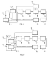
- Examples of the block layout of both versions of the device for automatic testing of power capacitors are shown in attached drawings. Version with the parallel oscillating circuit is in
fig. 1 and version with the series oscillating circuit is infig. 2 . - Layout of the device for automatic testing of power capacitors suitable especially for power capacitors with high capacitance, which are tested using the current with tens or even hundreds of A, is shown in
fig. 1 . The testedpower capacitor 1 is complemented with an inductor 3 with low losses, the inductance of which is selected such that at the testing frequency it has the same reactance as the testedpower capacitor 1, to form a parallel oscillating circuit, in which at the circuit's oscillating frequency the capacitance reactive power of the testedpower capacitor 1 is compensated by the inductance reactive power of the inductor 3. In the series combination with the testedpower capacitor 1, which is connected in parallel with the inductor 3, is inserted the first current sensor 2.1 by its input terminals. The output of the first current sensor 2.1 is connected both to the input of the regulatingamplifier 9 and to one input of thephase detector 10. To one of the connections between the created parallel oscillating circuit and the output of thepower amplifier 6 is connected the second current sensor 4.1 by its input terminals. Its output is connected to the second input of thephase detector 10. The output of thephase detector 10 is via the integratingamplifier 11 and voltage-controlledoscillator 8 connected to one input of the adjustable attenuatingelement 7. To the second input of the adjustable attenuatingelement 7 is connected the output of the regulatingamplifier 9. The output of the adjustableattenuating element 7 is in the basic design connected via thepower amplifier 6 to the common connection of the inductor 3 and the first current sensor 2.1 and to the second input of the second current sensor 4.1. In connection according to thefig. 1 is thispower amplifier 6 connected to the parallel oscillating circuit formed by the testedpower capacitor 1 and the inductor 3 via the matching transformingelement 5. - The testing signal is generated by the voltage-controlled
oscillator 8, from which it is led to the adjustable attenuatingelement 7,power amplifier 6, in the given example also to the matching transformingelement 5, and from here up to the parallel oscillating circuit with thepower capacitor 1 and the inductor 3. The in-tune condition of the oscillating circuit is monitored by the current sensors, it means the first current sensor 2.1 and the second current sensor 4.1, while their output signals reflect the current in the testedpower capacitor 1 and the excitation current of the parallel oscillating circuit. Both these signals are led to thephase detector 10 where its output signal is proportionate to the deviation of the phase shift between the incoming signals from the value of 90°. The output signal of thephase detector 10 is led to the integratingamplifier 11, which generates a control signal that automatically sets the frequency of the voltage-controlledoscillator 8 to the oscillating frequency of the measuring circuit. The output signal of the first current sensor 2.1 is then led to the regulatingamplifier 9 where it is compared with the reference level and based on the difference the control signal for theadjustable attenuating element 7 is generated, which continuously sets the input voltage of thepower amplifier 6 to the value, at which the current in thepower capacitor 1 reaches desired value. - Matching the oscillating resistance of the oscillating circuit with the optimal load resistance of the signal source is provided by the
matching transforming element 5, which is inserted between thepower amplifier 6 and the measuring oscillating circuit. Transformation ratio of thematching transforming element 5 is chosen such that the oscillating resistance of the oscillating circuit at oscillation, which it transforms, corresponds to the optimal load resistance of thepower amplifier 6. - Layout of the device for automatic testing of power capacitors suitable especially for power capacitors with lower capacitance, which are tested using the current of several A and during testing they feature voltage up to several thousand V, is shown in
fig. 2 . The capacitance reactance of thepower capacitor 1 is at the testing frequency higher than the optimal load resistance of thepower amplifier 6. In this case the testedpower capacitor 1 is complemented with inductor 3 with low losses, the loss factor of which is comparable with the loss factor of the testedpower capacitor 1 or lower, to form a series oscillating circuit. The inductance of the inductor is selected such that at the testing frequency it has the same reactance as the testedpower capacitor 1. In thus created series oscillating circuit the capacitance reactive power of the capacitor at the oscillating frequency is compensated by the inductance reactive power of the inductor. The inductor 3 is bridged with the first voltage sensor 2.2, the output of which is connected both to the input of the regulatingamplifier 9 and to one input of thephase detector 10. In parallel with this series oscillating circuit is connected the second voltage sensor 4.2, the output of which is connected to the second input of thephase detector 10. The output of thephase detector 10 is via the integratingamplifier 11 and the voltage-controlledoscillator 8 connected to one input of theadjustable attenuating element 7 . To the second input of theadjustable attenuating element 7 is connected the output of the regulatingamplifier 9. The output of theadjustable attenuating element 7 is connected to the input of thepower amplifier 6, the output of which is in the given example connected to the series oscillating circuit formed by the testedpower capacitor 1 and the inductor 3 via thematching transforming element 5. - The testing signal is again generated by the voltage-controlled
oscillator 8, from which it is led to theadjustable attenuating element 7,power amplifier 6, thematching transforming element 5, and from here up to the series oscillating circuit with thepower capacitor 1 and the inductor 3. The in-tune condition of the series oscillating circuit is monitored by the voltage sensors, it means the first voltage sensor 2.2 and the second voltage sensor 4.2, while their output signals reflect the voltage at the testedpower capacitor 1 and the excitation voltage of the series oscillating circuit. Both these signals are led to thephase detector 10 where its output signal is proportionate to the deviation of the phase shift between the incoming signals from the value of 90°. The output signal of thephase detector 10 is led to the integratingamplifier 11, which generates a control signal that automatically sets the frequency of the voltage-controlledoscillator 8 to the oscillating frequency of the measuring circuit. The output signal of the first voltage sensor 2.2 is then led to the regulatingamplifier 9 where it is compared with the reference level and based on the difference the control signal for theadjustable attenuating element 7 is generated, which continuously sets the input voltage of thepower amplifier 6 to the value, at which the voltage at thepower capacitor 1 reaches desired value. Thematching transforming element 5 here has the same role as in the design according to thefig. 1 . - The principle of function of the device for automatic testing of power capacitors is excitation of desired high reactive power in the tested
power capacitor 1, which is part of an oscillating circuit, by action of many times lower real power, which covers the losses in thepower capacitor 1 and the inductor 3 of the oscillating circuit. Because modern and quality capacitors with dielectrics made of plastic foils feature within the range of measuring frequencies from 1 to 100 kHz low loss factor with theorder 10-3, the power losses of the testing circuit do not exceed 100 W and the losses in the capacitor usually consume only smaller part of the excitation power. Greater part of the excitation power, roughly 60-80%, is formed by the power losses of the inductor 3, which usually has 2 to 3 times greater loss factor than the testedpower capacitor 1. - If the oscillating circuit is precisely tuned at the measuring frequency, it is possible to use the real power of 100 W to create the reactive power in the tested
power capacitor 1 at the level of 5 to 10 kVAr. Automatic ensuring that the in-tune condition is permanently fulfilled, matching the oscillating resistance of the oscillating circuit with the optimal load resistance of the signal source and stabilization of the signal level in the measuring circuit are the basic functions of the device for automatic testing of power capacitors. - The loop providing the automatic fine tuning sets the instantaneous value of the measuring frequency to the oscillating frequency of the oscillating circuit, which during testing may slightly vary due to the capacitor's ageing, change of its capacitance or change of the inductor's inductance. With respect to the quality factor of the measuring oscillating circuit, which may reach even values higher than 100, even the variation in order of tenths % between the measuring frequency and the oscillating frequency of the measuring circuit considerable variation of the oscillator circuit impedance from the real value. Because automatic electronic setting of inductance or capacitance in the measuring circuit would be difficult and costly, it is the measuring frequency that is being set to the oscillating frequency. If the change of the measuring frequency is low, usually not over 1%, then also the changes of measuring conditions caused by such change are negligible.
- The oscillation conditions in the oscillating circuit formed by the
capacitor 1 and the inductor 3 are monitored by means of current sensors 2.1, 4.1 or voltage sensors 2.2, 4.2, while their output signals reflect the current or voltage on the testedpower capacitor 1 and the excitation current or excitation voltage of the oscillating circuit. Output signals of the current sensors 2.1, 4.1 or voltage sensors 2.2, 4.2 are led to thephase detector 10, which functions as an analogue multiplier, its output voltage is zero provided that the phase shift of the input signals is 90° and provided that the oscillating circuit is tuned at the frequency of the excitation signal. For other and small deviations of the phase shift from 90°, if the oscillating circuit is not tuned at the excitation signal frequency, the output voltage is proportionate to the size of actual phase shift from 90°, or also to the deviation of the oscillating frequency of the oscillating circuit from the excitation signal frequency respectively. Output signal of thephase detector 10 is therefore used as the input quantity in the loop providing automatic fine tuning and is led to the integratingamplifier 11, which generates the control signal used to automatically set the frequency of the voltage-controlledoscillator 8 to the oscillating frequency of the measuring circuit. - The loop providing stabilization of the signal level in the measuring circuit ensures long-term constant level of the signal on the tested
power capacitor 1 even during minor changes of the measuring circuit parameters. Output signal of the first current sensor 2.1, or of the first voltage sensor 2.2 respectively, which represents the signal level on the testedpower capacitor 1, is evaluated and compared with the reference level in the regulatingamplifier 9. Here, based on the difference, control signal is generated and led to theadjustable attenuating element 7 and its attenuation is adapted according to the level of the control voltage. This ensures continuous adjusting of the input voltage of thepower amplifier 6 to the value, at which the current in the testedpower capacitor 1 reaches desired value. - The device according to the presented solution is a device for automatic testing of power capacitors that can be deployed in all cases where quality capacitors are subject to long-term tests, e.g. during the life cycle testing, by reactive power higher than several tens VAr. The device allows for testing with lower power of the excitation signal generator and with lower electric power consumption than other solutions. In addition, the device allows for stabilization of the tested capacitor load level during testing.
Claims (4)
- Device for automatic testing of power capacitors characterized by the fact that for testing the power capacitors with high capacitance, the reactance of which at the testing frequency is lower than the optimal load resistance of the power amplifier (6) inserted in the device, the tested power capacitor (1) is complemented to the parallel oscillating circuit with the inductor (3) with low losses and the loss factor comparable to the loss factor of the tested power capacitor (1) or lower, where the inductor's (3) inductance value is selected such that at the testing frequency it has the same reactance as the tested power capacitor (1), where to the series combination with the tested power capacitor (1) connected in parallel with the inductor (3) is inserted the first current sensor (2.1) by its input terminals, the output of which is connected both to the input of the regulating amplifier (9) and to one input of the phase detector (10) and where to one of the connections between the parallel oscillating circuit and the output of the power amplifier (6) is connected the second current sensor (4.1) by its input terminals, the output of which is connected to the second input of the phase detector (10) and the output of the phase detector (10) is via the integrating amplifier (11) and the voltage-controlled oscillator (8) connected to one input of the adjustable attenuating element (7), while to its second input is connected the output of the regulating amplifier (9), and where the output of the adjustable attenuating element (7) is connected via the power amplifier (6) to the common connection of the inductor (3) and the first current sensor (2.1) and to the second input of the second current sensor (4.1).
- Device according to claim 1 characterized by the fact that the power amplifier (6) is connected to the parallel oscillating circuit formed by the tested power capacitor (1) and the inductor (3) via the matching transforming element (5).
- Device for automatic testing of power capacitors characterized by the fact that for testing the power capacitors with lower capacitance, the reactance of which at the testing frequency is higher than the optimal load resistance of the power amplifier (6) inserted in the device, the tested power capacitor (1) is complemented to the series oscillating circuit with the inductor (3) with low losses and the loss factor comparable to the loss factor of the tested power capacitor (1) or lower, where the inductor's (3) inductance value is selected such that at the testing frequency it has the same reactance as the tested power capacitor (1), where the inductor (3) is bridged by the first voltage sensor (2.2), the output of which is connected both to the input of the regulating amplifier (9) and to one input of the phase detector (10) and in parallel with this series oscillating circuit is connected the second voltage sensor (4.2) by its input terminals, the output of which is connected to the second input of the phase detector (10) and the output of the phase detector (10) is via the integrating amplifier (11) and the voltage-controlled oscillator (8) connected to one input of the adjustable attenuating element (7), while to its second input is connected the output of the regulating amplifier (9), and where the output of the adjustable attenuating element (7) is connected to the input of the power amplifier (6), the output of which is connected to the series oscillating circuit.
- Device according to claim 3 characterized by the fact that the power amplifier (6) is connected to the series oscillating circuit formed by the tested power capacitor (1) and the inductor (3) via the matching transforming element (5).
Applications Claiming Priority (1)
| Application Number | Priority Date | Filing Date | Title |
|---|---|---|---|
| CZ2013-84A CZ201384A3 (en) | 2013-02-07 | 2013-02-07 | Device for automatic testing power capacitors |
Publications (3)
| Publication Number | Publication Date |
|---|---|
| EP2765428A2 true EP2765428A2 (en) | 2014-08-13 |
| EP2765428A3 EP2765428A3 (en) | 2018-01-03 |
| EP2765428B1 EP2765428B1 (en) | 2019-09-25 |
Family
ID=49920216
Family Applications (1)
| Application Number | Title | Priority Date | Filing Date |
|---|---|---|---|
| EP14150931.5A Active EP2765428B1 (en) | 2013-02-07 | 2014-01-13 | Device for automatic testing of power capacitors |
Country Status (2)
| Country | Link |
|---|---|
| EP (1) | EP2765428B1 (en) |
| CZ (1) | CZ201384A3 (en) |
Cited By (2)
| Publication number | Priority date | Publication date | Assignee | Title |
|---|---|---|---|---|
| CN110412359A (en) * | 2019-08-29 | 2019-11-05 | 日新电机(无锡)有限公司 | Test device and system for measuring the inherent inductance of metallized film capacitors |
| CN115902480A (en) * | 2022-11-29 | 2023-04-04 | 西安西电电力电容器有限责任公司 | An integrated power capacitor test circuit and its tuning method |
Families Citing this family (2)
| Publication number | Priority date | Publication date | Assignee | Title |
|---|---|---|---|---|
| EP3866329B1 (en) | 2020-02-12 | 2025-06-11 | Hamilton Sundstrand Corporation | Motor drive |
| CN114966214B (en) * | 2022-06-13 | 2025-06-17 | 西南交通大学 | A broadband harmonic disturbance device and control method |
Family Cites Families (11)
| Publication number | Priority date | Publication date | Assignee | Title |
|---|---|---|---|---|
| US3970925A (en) * | 1974-05-10 | 1976-07-20 | Control Data Corporation | Direct reading reactance meter |
| FR2576690B1 (en) * | 1985-01-29 | 1988-04-01 | Veglia | REACTANCE MEASURING DEVICE |
| JPS61266965A (en) * | 1985-05-22 | 1986-11-26 | Sanwa Denki Seisakusho:Kk | Impedance measuring instrument |
| JPH06213978A (en) * | 1993-01-19 | 1994-08-05 | Fuji Electric Co Ltd | Switch test circuit |
| GB9316036D0 (en) * | 1993-08-03 | 1993-09-15 | Univ Birmingham | Measurement apparatus |
| SE515388C2 (en) * | 1995-09-14 | 2001-07-23 | Abb Research Ltd | Device for sensing electrical discharges in a sample object |
| DE102004047116A1 (en) * | 2004-03-08 | 2005-10-06 | Micro-Epsilon Messtechnik Gmbh & Co Kg | Method and device for non-contact speed measurement |
| JP4975824B2 (en) * | 2007-10-18 | 2012-07-11 | パイオニア株式会社 | Capacitance detection device |
| US8351232B2 (en) * | 2009-12-28 | 2013-01-08 | Nxp B.V. | Power factor corrector with high power factor at low load or high mains voltage conditions |
| CN202721445U (en) * | 2012-05-23 | 2013-02-06 | 杭州晟泰电气有限公司 | Intelligent reactive power compensation integrated module |
| CN102736000B (en) * | 2012-07-06 | 2014-10-08 | 桂林电子科技大学 | On-line detection method and device for power capacitor |
-
2013
- 2013-02-07 CZ CZ2013-84A patent/CZ201384A3/en not_active IP Right Cessation
-
2014
- 2014-01-13 EP EP14150931.5A patent/EP2765428B1/en active Active
Non-Patent Citations (1)
| Title |
|---|
| None |
Cited By (3)
| Publication number | Priority date | Publication date | Assignee | Title |
|---|---|---|---|---|
| CN110412359A (en) * | 2019-08-29 | 2019-11-05 | 日新电机(无锡)有限公司 | Test device and system for measuring the inherent inductance of metallized film capacitors |
| CN115902480A (en) * | 2022-11-29 | 2023-04-04 | 西安西电电力电容器有限责任公司 | An integrated power capacitor test circuit and its tuning method |
| CN115902480B (en) * | 2022-11-29 | 2023-11-03 | 西安西电电力电容器有限责任公司 | Integrated power capacitor test loop and tuning method thereof |
Also Published As
| Publication number | Publication date |
|---|---|
| EP2765428A3 (en) | 2018-01-03 |
| EP2765428B1 (en) | 2019-09-25 |
| CZ304363B6 (en) | 2014-03-26 |
| CZ201384A3 (en) | 2014-03-26 |
Similar Documents
| Publication | Publication Date | Title |
|---|---|---|
| EP2765428A2 (en) | Device for automatic testing of power capacitors | |
| US5128611A (en) | Electronic electricity meter | |
| KR20080029790A (en) | Matching Network Characterization Using Variable Impedance Analysis | |
| KR20180040149A (en) | Electronic control device | |
| CN104136931A (en) | Test system and method for testing high-voltage technology devices | |
| US6938462B2 (en) | Device for measuring viscosity and/or density | |
| KR20180039069A (en) | Devices for measuring measurement variables | |
| CN108282028A (en) | The tuning methods and system of resonance type wireless electric energy transmission based on current amplitude | |
| KR101930440B1 (en) | Apparatus of supplying power for generating plasma | |
| US9231520B2 (en) | Wien-bridge oscillator and circuit arrangement for regulating a detuning | |
| US5872456A (en) | Apparatus for directly measuring component values within an RF circuit | |
| US20080211598A1 (en) | On-chip impedance matching using a variable capacitor | |
| US9523733B2 (en) | Automatic test equipment for testing an oscillating crystal and method for operating the same | |
| JP6159472B2 (en) | Circuit apparatus and method for controlling piezoelectric transformer | |
| EP2833545A1 (en) | Device and method for oscillation margin testing of a crystal oscillator | |
| US7218015B2 (en) | Method of providing a constant AC voltage to a remote variable load | |
| JP2010261761A (en) | Output voltage measuring device | |
| CZ25418U1 (en) | Apparatus for automatic testing power capacitors | |
| US6208153B1 (en) | System for fast piezoelectric-resonator parameter measurements | |
| US11239688B2 (en) | Power supply unit with adaptive feedback control | |
| CA2755382C (en) | Instrumentation circuit for shunt-based metrology measurement | |
| RU2707394C2 (en) | Generator | |
| US2815479A (en) | High voltage supply | |
| Sotner et al. | Fractional-order phase shifters with constant magnitude frequency responses | |
| JP6148090B2 (en) | High frequency power supply |
Legal Events
| Date | Code | Title | Description |
|---|---|---|---|
| PUAI | Public reference made under article 153(3) epc to a published international application that has entered the european phase |
Free format text: ORIGINAL CODE: 0009012 |
|
| 17P | Request for examination filed |
Effective date: 20140115 |
|
| AK | Designated contracting states |
Kind code of ref document: A2 Designated state(s): AL AT BE BG CH CY CZ DE DK EE ES FI FR GB GR HR HU IE IS IT LI LT LU LV MC MK MT NL NO PL PT RO RS SE SI SK SM TR |
|
| AX | Request for extension of the european patent |
Extension state: BA ME |
|
| PUAL | Search report despatched |
Free format text: ORIGINAL CODE: 0009013 |
|
| AK | Designated contracting states |
Kind code of ref document: A3 Designated state(s): AL AT BE BG CH CY CZ DE DK EE ES FI FR GB GR HR HU IE IS IT LI LT LU LV MC MK MT NL NO PL PT RO RS SE SI SK SM TR |
|
| AX | Request for extension of the european patent |
Extension state: BA ME |
|
| RIC1 | Information provided on ipc code assigned before grant |
Ipc: G01R 31/02 20060101AFI20171127BHEP |
|
| STAA | Information on the status of an ep patent application or granted ep patent |
Free format text: STATUS: EXAMINATION IS IN PROGRESS |
|
| 17Q | First examination report despatched |
Effective date: 20180227 |
|
| GRAP | Despatch of communication of intention to grant a patent |
Free format text: ORIGINAL CODE: EPIDOSNIGR1 |
|
| STAA | Information on the status of an ep patent application or granted ep patent |
Free format text: STATUS: GRANT OF PATENT IS INTENDED |
|
| GRAS | Grant fee paid |
Free format text: ORIGINAL CODE: EPIDOSNIGR3 |
|
| GRAA | (expected) grant |
Free format text: ORIGINAL CODE: 0009210 |
|
| STAA | Information on the status of an ep patent application or granted ep patent |
Free format text: STATUS: THE PATENT HAS BEEN GRANTED |
|
| INTG | Intention to grant announced |
Effective date: 20190730 |
|
| AK | Designated contracting states |
Kind code of ref document: B1 Designated state(s): AL AT BE BG CH CY CZ DE DK EE ES FI FR GB GR HR HU IE IS IT LI LT LU LV MC MK MT NL NO PL PT RO RS SE SI SK SM TR |
|
| REG | Reference to a national code |
Ref country code: GB Ref legal event code: FG4D |
|
| REG | Reference to a national code |
Ref country code: CH Ref legal event code: EP |
|
| REG | Reference to a national code |
Ref country code: AT Ref legal event code: REF Ref document number: 1184330 Country of ref document: AT Kind code of ref document: T Effective date: 20191015 |
|
| REG | Reference to a national code |
Ref country code: IE Ref legal event code: FG4D |
|
| REG | Reference to a national code |
Ref country code: DE Ref legal event code: R096 Ref document number: 602014054108 Country of ref document: DE |
|
| REG | Reference to a national code |
Ref country code: DE Ref legal event code: R079 Ref document number: 602014054108 Country of ref document: DE Free format text: PREVIOUS MAIN CLASS: G01R0031020000 Ipc: G01R0031500000 |
|
| REG | Reference to a national code |
Ref country code: NL Ref legal event code: MP Effective date: 20190925 |
|
| PG25 | Lapsed in a contracting state [announced via postgrant information from national office to epo] |
Ref country code: HR Free format text: LAPSE BECAUSE OF FAILURE TO SUBMIT A TRANSLATION OF THE DESCRIPTION OR TO PAY THE FEE WITHIN THE PRESCRIBED TIME-LIMIT Effective date: 20190925 Ref country code: SE Free format text: LAPSE BECAUSE OF FAILURE TO SUBMIT A TRANSLATION OF THE DESCRIPTION OR TO PAY THE FEE WITHIN THE PRESCRIBED TIME-LIMIT Effective date: 20190925 Ref country code: LT Free format text: LAPSE BECAUSE OF FAILURE TO SUBMIT A TRANSLATION OF THE DESCRIPTION OR TO PAY THE FEE WITHIN THE PRESCRIBED TIME-LIMIT Effective date: 20190925 Ref country code: FI Free format text: LAPSE BECAUSE OF FAILURE TO SUBMIT A TRANSLATION OF THE DESCRIPTION OR TO PAY THE FEE WITHIN THE PRESCRIBED TIME-LIMIT Effective date: 20190925 Ref country code: NO Free format text: LAPSE BECAUSE OF FAILURE TO SUBMIT A TRANSLATION OF THE DESCRIPTION OR TO PAY THE FEE WITHIN THE PRESCRIBED TIME-LIMIT Effective date: 20191225 Ref country code: BG Free format text: LAPSE BECAUSE OF FAILURE TO SUBMIT A TRANSLATION OF THE DESCRIPTION OR TO PAY THE FEE WITHIN THE PRESCRIBED TIME-LIMIT Effective date: 20191225 |
|
| REG | Reference to a national code |
Ref country code: LT Ref legal event code: MG4D |
|
| PG25 | Lapsed in a contracting state [announced via postgrant information from national office to epo] |
Ref country code: GR Free format text: LAPSE BECAUSE OF FAILURE TO SUBMIT A TRANSLATION OF THE DESCRIPTION OR TO PAY THE FEE WITHIN THE PRESCRIBED TIME-LIMIT Effective date: 20191226 Ref country code: RS Free format text: LAPSE BECAUSE OF FAILURE TO SUBMIT A TRANSLATION OF THE DESCRIPTION OR TO PAY THE FEE WITHIN THE PRESCRIBED TIME-LIMIT Effective date: 20190925 Ref country code: LV Free format text: LAPSE BECAUSE OF FAILURE TO SUBMIT A TRANSLATION OF THE DESCRIPTION OR TO PAY THE FEE WITHIN THE PRESCRIBED TIME-LIMIT Effective date: 20190925 |
|
| REG | Reference to a national code |
Ref country code: AT Ref legal event code: MK05 Ref document number: 1184330 Country of ref document: AT Kind code of ref document: T Effective date: 20190925 |
|
| PG25 | Lapsed in a contracting state [announced via postgrant information from national office to epo] |
Ref country code: NL Free format text: LAPSE BECAUSE OF FAILURE TO SUBMIT A TRANSLATION OF THE DESCRIPTION OR TO PAY THE FEE WITHIN THE PRESCRIBED TIME-LIMIT Effective date: 20190925 Ref country code: RO Free format text: LAPSE BECAUSE OF FAILURE TO SUBMIT A TRANSLATION OF THE DESCRIPTION OR TO PAY THE FEE WITHIN THE PRESCRIBED TIME-LIMIT Effective date: 20190925 Ref country code: ES Free format text: LAPSE BECAUSE OF FAILURE TO SUBMIT A TRANSLATION OF THE DESCRIPTION OR TO PAY THE FEE WITHIN THE PRESCRIBED TIME-LIMIT Effective date: 20190925 Ref country code: AT Free format text: LAPSE BECAUSE OF FAILURE TO SUBMIT A TRANSLATION OF THE DESCRIPTION OR TO PAY THE FEE WITHIN THE PRESCRIBED TIME-LIMIT Effective date: 20190925 Ref country code: EE Free format text: LAPSE BECAUSE OF FAILURE TO SUBMIT A TRANSLATION OF THE DESCRIPTION OR TO PAY THE FEE WITHIN THE PRESCRIBED TIME-LIMIT Effective date: 20190925 Ref country code: PL Free format text: LAPSE BECAUSE OF FAILURE TO SUBMIT A TRANSLATION OF THE DESCRIPTION OR TO PAY THE FEE WITHIN THE PRESCRIBED TIME-LIMIT Effective date: 20190925 Ref country code: AL Free format text: LAPSE BECAUSE OF FAILURE TO SUBMIT A TRANSLATION OF THE DESCRIPTION OR TO PAY THE FEE WITHIN THE PRESCRIBED TIME-LIMIT Effective date: 20190925 Ref country code: PT Free format text: LAPSE BECAUSE OF FAILURE TO SUBMIT A TRANSLATION OF THE DESCRIPTION OR TO PAY THE FEE WITHIN THE PRESCRIBED TIME-LIMIT Effective date: 20200127 Ref country code: IT Free format text: LAPSE BECAUSE OF FAILURE TO SUBMIT A TRANSLATION OF THE DESCRIPTION OR TO PAY THE FEE WITHIN THE PRESCRIBED TIME-LIMIT Effective date: 20190925 |
|
| PGFP | Annual fee paid to national office [announced via postgrant information from national office to epo] |
Ref country code: GB Payment date: 20191112 Year of fee payment: 7 |
|
| PG25 | Lapsed in a contracting state [announced via postgrant information from national office to epo] |
Ref country code: SK Free format text: LAPSE BECAUSE OF FAILURE TO SUBMIT A TRANSLATION OF THE DESCRIPTION OR TO PAY THE FEE WITHIN THE PRESCRIBED TIME-LIMIT Effective date: 20190925 Ref country code: SM Free format text: LAPSE BECAUSE OF FAILURE TO SUBMIT A TRANSLATION OF THE DESCRIPTION OR TO PAY THE FEE WITHIN THE PRESCRIBED TIME-LIMIT Effective date: 20190925 Ref country code: CZ Free format text: LAPSE BECAUSE OF FAILURE TO SUBMIT A TRANSLATION OF THE DESCRIPTION OR TO PAY THE FEE WITHIN THE PRESCRIBED TIME-LIMIT Effective date: 20190925 Ref country code: IS Free format text: LAPSE BECAUSE OF FAILURE TO SUBMIT A TRANSLATION OF THE DESCRIPTION OR TO PAY THE FEE WITHIN THE PRESCRIBED TIME-LIMIT Effective date: 20200224 |
|
| REG | Reference to a national code |
Ref country code: DE Ref legal event code: R097 Ref document number: 602014054108 Country of ref document: DE |
|
| PGFP | Annual fee paid to national office [announced via postgrant information from national office to epo] |
Ref country code: FR Payment date: 20200122 Year of fee payment: 7 |
|
| PG2D | Information on lapse in contracting state deleted |
Ref country code: IS |
|
| PG25 | Lapsed in a contracting state [announced via postgrant information from national office to epo] |
Ref country code: IS Free format text: LAPSE BECAUSE OF FAILURE TO SUBMIT A TRANSLATION OF THE DESCRIPTION OR TO PAY THE FEE WITHIN THE PRESCRIBED TIME-LIMIT Effective date: 20200126 Ref country code: DK Free format text: LAPSE BECAUSE OF FAILURE TO SUBMIT A TRANSLATION OF THE DESCRIPTION OR TO PAY THE FEE WITHIN THE PRESCRIBED TIME-LIMIT Effective date: 20190925 |
|
| PLBE | No opposition filed within time limit |
Free format text: ORIGINAL CODE: 0009261 |
|
| STAA | Information on the status of an ep patent application or granted ep patent |
Free format text: STATUS: NO OPPOSITION FILED WITHIN TIME LIMIT |
|
| PG25 | Lapsed in a contracting state [announced via postgrant information from national office to epo] |
Ref country code: MC Free format text: LAPSE BECAUSE OF FAILURE TO SUBMIT A TRANSLATION OF THE DESCRIPTION OR TO PAY THE FEE WITHIN THE PRESCRIBED TIME-LIMIT Effective date: 20190925 |
|
| REG | Reference to a national code |
Ref country code: CH Ref legal event code: PL |
|
| 26N | No opposition filed |
Effective date: 20200626 |
|
| REG | Reference to a national code |
Ref country code: BE Ref legal event code: MM Effective date: 20200131 |
|
| PG25 | Lapsed in a contracting state [announced via postgrant information from national office to epo] |
Ref country code: LU Free format text: LAPSE BECAUSE OF NON-PAYMENT OF DUE FEES Effective date: 20200113 |
|
| PG25 | Lapsed in a contracting state [announced via postgrant information from national office to epo] |
Ref country code: SI Free format text: LAPSE BECAUSE OF FAILURE TO SUBMIT A TRANSLATION OF THE DESCRIPTION OR TO PAY THE FEE WITHIN THE PRESCRIBED TIME-LIMIT Effective date: 20190925 Ref country code: CH Free format text: LAPSE BECAUSE OF NON-PAYMENT OF DUE FEES Effective date: 20200131 Ref country code: LI Free format text: LAPSE BECAUSE OF NON-PAYMENT OF DUE FEES Effective date: 20200131 Ref country code: BE Free format text: LAPSE BECAUSE OF NON-PAYMENT OF DUE FEES Effective date: 20200131 |
|
| PG25 | Lapsed in a contracting state [announced via postgrant information from national office to epo] |
Ref country code: IE Free format text: LAPSE BECAUSE OF NON-PAYMENT OF DUE FEES Effective date: 20200113 |
|
| PGFP | Annual fee paid to national office [announced via postgrant information from national office to epo] |
Ref country code: DE Payment date: 20201207 Year of fee payment: 8 |
|
| GBPC | Gb: european patent ceased through non-payment of renewal fee |
Effective date: 20210113 |
|
| PG25 | Lapsed in a contracting state [announced via postgrant information from national office to epo] |
Ref country code: FR Free format text: LAPSE BECAUSE OF NON-PAYMENT OF DUE FEES Effective date: 20210131 |
|
| PG25 | Lapsed in a contracting state [announced via postgrant information from national office to epo] |
Ref country code: GB Free format text: LAPSE BECAUSE OF NON-PAYMENT OF DUE FEES Effective date: 20210113 |
|
| PG25 | Lapsed in a contracting state [announced via postgrant information from national office to epo] |
Ref country code: TR Free format text: LAPSE BECAUSE OF FAILURE TO SUBMIT A TRANSLATION OF THE DESCRIPTION OR TO PAY THE FEE WITHIN THE PRESCRIBED TIME-LIMIT Effective date: 20190925 Ref country code: MT Free format text: LAPSE BECAUSE OF FAILURE TO SUBMIT A TRANSLATION OF THE DESCRIPTION OR TO PAY THE FEE WITHIN THE PRESCRIBED TIME-LIMIT Effective date: 20190925 Ref country code: CY Free format text: LAPSE BECAUSE OF FAILURE TO SUBMIT A TRANSLATION OF THE DESCRIPTION OR TO PAY THE FEE WITHIN THE PRESCRIBED TIME-LIMIT Effective date: 20190925 |
|
| PG25 | Lapsed in a contracting state [announced via postgrant information from national office to epo] |
Ref country code: MK Free format text: LAPSE BECAUSE OF FAILURE TO SUBMIT A TRANSLATION OF THE DESCRIPTION OR TO PAY THE FEE WITHIN THE PRESCRIBED TIME-LIMIT Effective date: 20190925 |
|
| REG | Reference to a national code |
Ref country code: DE Ref legal event code: R119 Ref document number: 602014054108 Country of ref document: DE |
|
| PG25 | Lapsed in a contracting state [announced via postgrant information from national office to epo] |
Ref country code: DE Free format text: LAPSE BECAUSE OF NON-PAYMENT OF DUE FEES Effective date: 20220802 |