EP2762903A1 - Ac input voltage interruption detection method and circuit - Google Patents
Ac input voltage interruption detection method and circuit Download PDFInfo
- Publication number
- EP2762903A1 EP2762903A1 EP20120835190 EP12835190A EP2762903A1 EP 2762903 A1 EP2762903 A1 EP 2762903A1 EP 20120835190 EP20120835190 EP 20120835190 EP 12835190 A EP12835190 A EP 12835190A EP 2762903 A1 EP2762903 A1 EP 2762903A1
- Authority
- EP
- European Patent Office
- Prior art keywords
- voltage
- input voltage
- limit
- class
- circuit
- Prior art date
- Legal status (The legal status is an assumption and is not a legal conclusion. Google has not performed a legal analysis and makes no representation as to the accuracy of the status listed.)
- Granted
Links
Images




Classifications
-
- G—PHYSICS
- G01—MEASURING; TESTING
- G01R—MEASURING ELECTRIC VARIABLES; MEASURING MAGNETIC VARIABLES
- G01R19/00—Arrangements for measuring currents or voltages or for indicating presence or sign thereof
- G01R19/12—Measuring rate of change
-
- G—PHYSICS
- G01—MEASURING; TESTING
- G01R—MEASURING ELECTRIC VARIABLES; MEASURING MAGNETIC VARIABLES
- G01R19/00—Arrangements for measuring currents or voltages or for indicating presence or sign thereof
- G01R19/145—Indicating the presence of current or voltage
- G01R19/155—Indicating the presence of voltage
-
- G—PHYSICS
- G01—MEASURING; TESTING
- G01R—MEASURING ELECTRIC VARIABLES; MEASURING MAGNETIC VARIABLES
- G01R19/00—Arrangements for measuring currents or voltages or for indicating presence or sign thereof
- G01R19/165—Indicating that current or voltage is either above or below a predetermined value or within or outside a predetermined range of values
-
- G—PHYSICS
- G01—MEASURING; TESTING
- G01R—MEASURING ELECTRIC VARIABLES; MEASURING MAGNETIC VARIABLES
- G01R19/00—Arrangements for measuring currents or voltages or for indicating presence or sign thereof
- G01R19/165—Indicating that current or voltage is either above or below a predetermined value or within or outside a predetermined range of values
- G01R19/16528—Indicating that current or voltage is either above or below a predetermined value or within or outside a predetermined range of values using digital techniques or performing arithmetic operations
-
- H—ELECTRICITY
- H02—GENERATION; CONVERSION OR DISTRIBUTION OF ELECTRIC POWER
- H02M—APPARATUS FOR CONVERSION BETWEEN AC AND AC, BETWEEN AC AND DC, OR BETWEEN DC AND DC, AND FOR USE WITH MAINS OR SIMILAR POWER SUPPLY SYSTEMS; CONVERSION OF DC OR AC INPUT POWER INTO SURGE OUTPUT POWER; CONTROL OR REGULATION THEREOF
- H02M1/00—Details of apparatus for conversion
- H02M1/32—Means for protecting converters other than automatic disconnection
Definitions
- the present invention relates to an AC input voltage interruption detection method and a circuit that involve detecting interruption of AC input voltage, and, for instance, shutting off a power supply or discharging capacitor that has been brought to high voltage.
- AC input voltage interruption detection circuits are used for detecting interruption of AC input voltage, and for performing, for instance, shut off of a power supply that is connected with AC input voltage or discharge of capacitor that has been brought to high voltage, and are essential circuits for the safe operation of AC-DC converters and the like.
- Fig. 1 and Fig. 2 are diagrams for explaining a conventional first AC input voltage interruption detection circuit, and the operation thereof, as disclosed in Patent document 1.
- the voltage of a filter capacitor C0 follows AC voltage when AC input voltage is connected via a plug that is connected to an AC power supply.
- the AC voltage at that point in time is held at C0, after which the AC voltage is discharged gradually by way of resistors (R1 and R2, and R3 or R4).
- the AC input voltage is monitored by a detection circuit (detailed circuit illustrated on the right of Fig. 1 ) via a divided voltage Vin from resistors R1 and R2 by way of a connection point of these resistors.
- AC is determined to be interrupted if a state where Vin does not drop to or below a reference voltage Vref1 lasts for a predefined time that is longer than the AC period.
- the detailed circuit illustrated on the right of Fig. 1 has: a first comparator CMP1 having a hysteresis characteristic and having the input voltage Vin applied to an inverting input terminal thereof; a switch MOSFET Q1, a gate terminal whereof is connected to an output terminal of the comparator CMP1; a constant current source I1 connected between a MOSFET Q1 and a power supply voltage terminal VDD; and a capacitor C1 connected between a ground point and a join node N1 of Q1 and I1.
- the constant current source I1 charges the capacitor C1 at constant current in the period during which Q1 is off.
- the detailed circuit illustrated on the right of Fig. 1 also has: a second comparator CMP2 having a hysteresis characteristic and having the potential V1 applied to a non-inverting input terminal thereof; an open-drain output MOSFET Q2, a gate terminal whereof is connected an output terminal of the comparator CMP2; and a constant current source I2, a diode D3, and dividing resistors R5, R6, that generate the reference voltage Vref1 that is applied to the non-inverting input terminal of the first comparator CMP1 and a reference voltage Vref2 that is applied to the inverting input terminal of the second comparator CMP2; wherein the drain terminal of Q2 is connected to an output terminal OUT.
- a second comparator CMP2 having a hysteresis characteristic and having the potential V1 applied to a non-inverting input terminal thereof
- an open-drain output MOSFET Q2 a gate terminal whereof is connected an output terminal of the comparator CMP2
- the first comparator CMP1 operates by comparing the input voltage Vin and the reference voltage Vref1, such that when the input voltage Vin becomes higher than Vref1, the output of the comparator falls to a low level, and the MOSFET Q1 is switched off, and when Vin becomes lower than Vref1, the output of the comparator rises to a high level, and Q1 is switched on.
- Q1 is switched on, the charge of the capacitor C1 that is connected to the join node N1 of Q1 and I1 is withdrawn, and, as a result, the potential V1 of the node N1 changes to the ground potential.
- the second comparator CMP2 operates by comparing the potential V1 of the node N1 with the reference voltage Vref2, such that when V1 becomes higher than Vref2, the output of the comparator falls to a low level.
- the first comparator CMP1 detects an AC waveform and continuously outputs a pulse even if AC voltage drops somewhat, as in period T1 illustrated in Fig. 2 . Therefore, the potential V1 of the node N1 does not become higher than Vref2 through periodic resetting of the charge of the capacitor C1, and an output Vout remains at a high level.
- the AC waveform disappears, as in period T2 illustrated in Fig. 2
- the first comparator CMP1 outputs no more pulses, and the charge of the capacitor C1 is no longer reset. Accordingly, V1 becomes higher than Vref2, the output Vout changes to a low level, and interruption of the AC power supply (AC input voltage interruption) can be notified to the exterior.
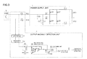
- Fig. 3 and Fig. 4 are diagrams for explaining a conventional second AC input voltage interruption detection circuit, and the operation thereof, as disclosed in Patent document 2.
- a ripple component of detected voltage is extracted by an AC detection unit (highpass filter), and it is determined that an and AC input voltage is connected if the voltage resulting from rectifying and smoothing the extracted ripple voltage exceeds a reference voltage Vr3.
- a differential amplifier 22 of the circuit of Fig. 3 works out, by way of an output voltage detection unit 11, a difference value of voltage-to-ground detection signals of output power supply lines PL1, PL2; a ripple component is detected by an AC detection unit 23; the ripple component is rectified and smoothed by a rectifying and smoothing unit 24; and a comparing unit 25 compares the result versus the reference voltage Vr3.
- a short-circuit fault occurs in a capacitor C3
- the line voltage between the output power supply lines PL1, PL2 becomes substantially zero, and the ripple component generated between the lines becomes likewise almost zero.
- the output signal level of the rectifying and smoothing unit 24 takes on a value of zero or close to zero, and a low-level alarm signal of occurrence of a capacitor short-circuit fault is outputted by the comparing unit 25.
- Fig. 4 is a waveform diagram illustrating the details of capacitor short-circuit fault detection of Fig. 3 . If capacitors C1 to C3 are in a normal condition, a DC voltage that comprises a switching frequency ripple component by switching elements Q1 to Q4 is applied to the output power supply lines PL1, PL2, and the detection signal by the output voltage detection unit 11 takes on a DC voltage that comprises the ripple component, as illustrated in (A), but becomes almost 0V when the capacitor C3 is shorted.
- the AC detection unit 23 detects the voltage comprised in the ripple component, as illustrated in (B), such that the detection signal becomes 0V upon shorting of the capacitor C3.
- the rectifying and smoothing output signal of the rectifying and smoothing unit 24 becomes 0V when the capacitor C3 is shorted, as illustrated in (C) and (D).
- the output signal of the comparing unit 25 that compares the rectifying and smoothing output signal with the reference voltage Vr3 is of a high level, as illustrated in (E), if the capacitor C3 is in a normal condition, but takes on a low level of 0V as a result of the occurrence of a short-circuit fault in the capacitor C3. This low-level signal is extracted as an alarm signal of occurrence of a capacitor short-circuit fault.
- the input voltage Vin may in some instances fail to drop down to the reference voltage Vref1, even if the AC input voltage is connected, when a time constant, which is based on a capacitive component (including a parasitic capacitance as well as a deliberately added capacitance for surge protection) that is present further toward the detection circuit side than the diodes D1, D2 and which is also based on the resistors (R1, R2) that discharge the capacitive component, is large.
- a time constant which is based on a capacitive component (including a parasitic capacitance as well as a deliberately added capacitance for surge protection) that is present further toward the detection circuit side than the diodes D1, D2 and which is also based on the resistors (R1, R2) that discharge the capacitive component.
- Patent document 1 Japanese Patent Application Publication No. 2009-165305 ( Fig. 1 to Fig. 3 )
- Patent document 2 Japanese Patent Application Publication No. 2009-89490 ( Fig. 2 and Fig. 4 ).
- an object of the present invention to provide an AC input voltage interruption detection method and circuit, suitable for being configured in the form of an integrated circuit, that enable interruption/connection of AC input voltage also in a case where the ripple of detected voltage is small (in a case where the detected voltage does not drop sufficiently).
- the AC input voltage interruption detection method of the present invention includes: determining to which class, from among three or more classes having predefined upper-limit voltages and lower-limit voltages respectively, a detected voltage that corresponds to an AC input voltage belongs, over a period shorter than the period of the AC input voltage, or constantly; and determining that the AC input voltage is interrupted when the class to which the detected voltage has been determined to belong does not change within a predefined time.
- the AC input voltage interruption detection method of the present invention is the method above, wherein when the detected voltage exceeds the upper-limit voltage the detected voltage is determined to belong to a next higher class, and when the detected voltage falls below the lower-limit voltage the detected voltage is determined to belong to a next lower class.
- the AC input voltage interruption detection method of the present invention allows determining interruption / connection of AC input voltage also in a case where the ripple of detected voltage of inputted AC is small (in a case where the detected voltage does not drop sufficiently).
- An AC input voltage interruption detection circuit of the present invention is an AC input voltage interruption detection circuit for carrying out an AC input voltage interruption detection method that involves determining to which class, from among three or more classes having predefined upper-limit voltages and lower-limit voltages respectively, a detected voltage that corresponds to an AC input voltage belongs, and determining that the AC input voltage is interrupted when the class to which the detected voltage has been determined to belong does not change within a predefined time, this AC input voltage interruption detection circuit including: an upper-limit voltage comparator circuit that determines that the detected voltage is higher than the upper-limit voltage; a lower-limit voltage comparator circuit that determines that the detected voltage is lower than the lower-limit voltage; an up/down counter that performs a count-up operation in accordance with an output result of the upper-limit voltage comparator circuit, and that performs a count-down operation in accordance with an output result of the lower-limit voltage comparator circuit; a digital-analog converter that outputs the upper-limit voltage and the lower-limit voltage in accordance with a digital value that is
- the upper-limit voltage comparator circuit and the lower-limit voltage comparator circuit are configured as one comparator by alternate use, in time division, of a comparator.
- sufficient hysteresis width is provided between the upper-limit voltage of a given class and the lower-limit voltage of the next higher class of the class.
- the circuit elements that make up the AC input voltage interruption detection circuit can be realized in the form of elements that are amenable to easy circuit integration, and hence the circuit elements can be easily realized the form of an integrated circuit.
- Fig. 5 is a diagram illustrating the configuration of an AC input voltage interruption detection circuit according to an embodiment of the present invention.
- the AC input voltage interruption detection circuit illustrated in Fig. 5 is made up of: a selector circuit 130 that selects either a class upper-limit voltage Vuref (151) or a class lower-limit voltage Vdref (152), as a reference voltage of a comparator 110, and that outputs the selection as a selector circuit output (131); a control logic 120 that controls the selector circuit 130, and that generates a count-up signal 121 or count-down signal 122 in accordance with the output of the comparator 110; an up/down counter 140 that counts up upon reception of the count-up signal 121 from the control logic 120, and that counts down upon reception of the count-down signal 122; a digital-analog converter 150 that outputs the class upper-limit voltage Vuref (151) and the class lower-limit voltage Vdref (152) in accordance with the digital value that is outputted by the up/down counter 140; and
- Fig. 5 illustrates an example wherein the timer circuit 160 is reset by the count-up signal 121 from the control logic 120.
- the timer circuit 160 is not limited thereto, and may be reset by the count-down signal 122 from the control logic 120.
- the timer circuit 160 may be reset by the result of a logical sum of the count-up signal 121 and the count-down signal 122.
- the detection signal Vin is voltage resulting from dividing the AC input voltage according in accordance with full-wave rectification or half-wave rectification. For instance, it is possible to detect divided voltage resulting from full-wave rectification in the same way as in the circuit illustrated in Fig.
- the control logic 120 repeats the operations (1) to (4) below over a short enough period with respect to the period of the AC input voltage (on the premise that this is not problematic in terms of the response speed of the comparator 110).
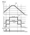
- Fig. 6 is a diagram illustrating an operation waveform of the AC input voltage interruption detection circuit illustrated in Fig. 5 .
- the broken lines parallel to the abscissa axis (time axis) of Fig. 6 are graph grid lines.
- Fig. 6 illustrates the manner (middle section in the illustrated example) in which the class upper-limit voltage Vuref (151) and the class lower-limit voltage Vdref (152) vary with respect to the detection signal Vin (100) that is depicted at the top of the illustrated example.
- the detection signal Vin (100) exhibits a change such that the detection signal Vin (100) has a magnitude comparable to that of a predefined period. Therefore, the count-up signal 121 and the count-down signal 122 are outputted by the control logic 120.
- Fig. 6 illustrates the reset signal 121 at the bottom.
- the timer circuit 160 is configured to be reset by the count-up signal 121 (or the count-down signal 122), and hence no time-out occurs while the AC input voltage is connected.
- the timer circuit 160 times out, for instance, when a time-count of 50 ms to 100 ms is reached, without generation of the count-up signal 121 and the count-down signal 122 by the control logic 120, and an AC interruption detection signal 161 is outputted by the timer circuit 160.
- the upper-limit voltage Vuref (151) and the lower-limit voltage Vdref (152) each have three classes (digital values).
- the value of the upper-limit voltage Vuref (151) corresponding to a given class (digital value) is set to a slightly higher value than the value of the lower-limit voltage Vdref (152) corresponding to the next higher class (digital value).
- a difference arises between the level at which the count-up signal 121 is generated during rising of the detection signal Vin
- the upper-limit voltage comparator circuit and the lower-limit voltage comparator circuit have been explained in a configuration example in which one comparator 110 is used in time-division, through the use of the control logic 120 and the selector circuit 130.
- the upper-limit voltage comparator circuit and the lower-limit voltage comparator circuit may be configured out of different comparators. In this case, it becomes possible to constantly determine (not discretely, as described above) to which class, from among three or more classes having predefined upper-limit voltages and lower-limit voltages respectively, a detected voltage that corresponds to an AC input voltage belongs.
- the above-described hysteresis width is preferably set to be somewhat large, to account for the influence of offset variability among the comparators.
- the AC input voltage interruption detection method and a circuit of the present invention are not limited to being compliant with Japanese specifications, where power supply specifications for AC input voltage ranges are narrow, but can also be suitably used in a wide variety of worldwide-compliant power-supply specifications.
Landscapes
- Physics & Mathematics (AREA)
- General Physics & Mathematics (AREA)
- Measurement Of Current Or Voltage (AREA)
Abstract
Description
- The present invention relates to an AC input voltage interruption detection method and a circuit that involve detecting interruption of AC input voltage, and, for instance, shutting off a power supply or discharging capacitor that has been brought to high voltage.
- AC input voltage interruption detection circuits are used for detecting interruption of AC input voltage, and for performing, for instance, shut off of a power supply that is connected with AC input voltage or discharge of capacitor that has been brought to high voltage, and are essential circuits for the safe operation of AC-DC converters and the like.
-
Fig. 1 andFig. 2 are diagrams for explaining a conventional first AC input voltage interruption detection circuit, and the operation thereof, as disclosed in Patent document 1. InFig. 1 , the voltage of a filter capacitor C0 follows AC voltage when AC input voltage is connected via a plug that is connected to an AC power supply. However, when the AC input voltage is interrupted for any reason, the AC voltage at that point in time is held at C0, after which the AC voltage is discharged gradually by way of resistors (R1 and R2, and R3 or R4). The AC input voltage is monitored by a detection circuit (detailed circuit illustrated on the right ofFig. 1 ) via a divided voltage Vin from resistors R1 and R2 by way of a connection point of these resistors. As illustrated on the right end ofFig. 2 , AC is determined to be interrupted if a state where Vin does not drop to or below a reference voltage Vref1 lasts for a predefined time that is longer than the AC period. - In a more detailed explanation, the detailed circuit illustrated on the right of
Fig. 1 has: a first comparator CMP1 having a hysteresis characteristic and having the input voltage Vin applied to an inverting input terminal thereof; a switch MOSFET Q1, a gate terminal whereof is connected to an output terminal of the comparator CMP1; a constant current source I1 connected between a MOSFET Q1 and a power supply voltage terminal VDD; and a capacitor C1 connected between a ground point and a join node N1 of Q1 and I1. The constant current source I1 charges the capacitor C1 at constant current in the period during which Q1 is off. As a result, when a potential V1 at the node N1 rises gradually and Q1 is switched on, the charge of the capacitor C1 is discharged, whereby the potential V1 is lowered rapidly, to generate thereby a sawtooth signal. - The detailed circuit illustrated on the right of
Fig. 1 also has: a second comparator CMP2 having a hysteresis characteristic and having the potential V1 applied to a non-inverting input terminal thereof; an open-drain output MOSFET Q2, a gate terminal whereof is connected an output terminal of the comparator CMP2; and a constant current source I2, a diode D3, and dividing resistors R5, R6, that generate the reference voltage Vref1 that is applied to the non-inverting input terminal of the first comparator CMP1 and a reference voltage Vref2 that is applied to the inverting input terminal of the second comparator CMP2; wherein the drain terminal of Q2 is connected to an output terminal OUT. - The first comparator CMP1 operates by comparing the input voltage Vin and the reference voltage Vref1, such that when the input voltage Vin becomes higher than Vref1, the output of the comparator falls to a low level, and the MOSFET Q1 is switched off, and when Vin becomes lower than Vref1, the output of the comparator rises to a high level, and Q1 is switched on. When Q1 is switched on, the charge of the capacitor C1 that is connected to the join node N1 of Q1 and I1 is withdrawn, and, as a result, the potential V1 of the node N1 changes to the ground potential. The second comparator CMP2 operates by comparing the potential V1 of the node N1 with the reference voltage Vref2, such that when V1 becomes higher than Vref2, the output of the comparator falls to a low level.
- In a further explanation of the operation of the above circuit configuration, the first comparator CMP1 detects an AC waveform and continuously outputs a pulse even if AC voltage drops somewhat, as in period T1 illustrated in
Fig. 2 . Therefore, the potential V1 of the node N1 does not become higher than Vref2 through periodic resetting of the charge of the capacitor C1, and an output Vout remains at a high level. When, by contrast, the AC waveform disappears, as in period T2 illustrated inFig. 2 , the first comparator CMP1 outputs no more pulses, and the charge of the capacitor C1 is no longer reset. Accordingly, V1 becomes higher than Vref2, the output Vout changes to a low level, and interruption of the AC power supply (AC input voltage interruption) can be notified to the exterior. -
Fig. 3 andFig. 4 are diagrams for explaining a conventional second AC input voltage interruption detection circuit, and the operation thereof, as disclosed inPatent document 2. In the circuit shown inFig. 3 , unlike in the case of the conventional first AC input voltage interruption detection circuit illustrated inFig. 1 , a ripple component of detected voltage is extracted by an AC detection unit (highpass filter), and it is determined that an and AC input voltage is connected if the voltage resulting from rectifying and smoothing the extracted ripple voltage exceeds a reference voltage Vr3. - In a more detailed explanation, a
differential amplifier 22 of the circuit ofFig. 3 works out, by way of an output voltage detection unit 11, a difference value of voltage-to-ground detection signals of output power supply lines PL1, PL2; a ripple component is detected by anAC detection unit 23; the ripple component is rectified and smoothed by a rectifying and smoothing unit 24; and a comparingunit 25 compares the result versus the reference voltage Vr3. When a short-circuit fault occurs in a capacitor C3, however, the line voltage between the output power supply lines PL1, PL2 becomes substantially zero, and the ripple component generated between the lines becomes likewise almost zero. As a result, the output signal level of the rectifying and smoothing unit 24 takes on a value of zero or close to zero, and a low-level alarm signal of occurrence of a capacitor short-circuit fault is outputted by the comparingunit 25. -
Fig. 4 is a waveform diagram illustrating the details of capacitor short-circuit fault detection ofFig. 3 . If capacitors C1 to C3 are in a normal condition, a DC voltage that comprises a switching frequency ripple component by switching elements Q1 to Q4 is applied to the output power supply lines PL1, PL2, and the detection signal by the output voltage detection unit 11 takes on a DC voltage that comprises the ripple component, as illustrated in (A), but becomes almost 0V when the capacitor C3 is shorted. TheAC detection unit 23 detects the voltage comprised in the ripple component, as illustrated in (B), such that the detection signal becomes 0V upon shorting of the capacitor C3. As a result, the rectifying and smoothing output signal of the rectifying and smoothing unit 24 becomes 0V when the capacitor C3 is shorted, as illustrated in (C) and (D). The output signal of the comparingunit 25 that compares the rectifying and smoothing output signal with the reference voltage Vr3 is of a high level, as illustrated in (E), if the capacitor C3 is in a normal condition, but takes on a low level of 0V as a result of the occurrence of a short-circuit fault in the capacitor C3. This low-level signal is extracted as an alarm signal of occurrence of a capacitor short-circuit fault. - In the conventional second AC detection circuit scheme described above, the occurrence of the capacitor short-circuit fault is detected through extraction of a ripple component alone. As a result, the below-described problem does not occur, as does in the conventional first AC input voltage interruption detection circuit illustrated in
Fig. 1 , where the detected voltage is compared with a fixed level. - In the above conventional first AC input voltage interruption detection circuit, the input voltage Vin may in some instances fail to drop down to the reference voltage Vref1, even if the AC input voltage is connected, when a time constant, which is based on a capacitive component (including a parasitic capacitance as well as a deliberately added capacitance for surge protection) that is present further toward the detection circuit side than the diodes D1, D2 and which is also based on the resistors (R1, R2) that discharge the capacitive component, is large. In such a case, a problem arises where erroneous determination is made that the AC input voltage is interrupted. If the circuit is used with fixed AC voltage, this problem can be avoided by selecting a reference voltage Vref1 corresponding to a voltage that is slightly lower than the peak value of the AC input voltage, but a problem arises then in that the choice of the reference voltage Vref1 becomes difficult when the AC input voltage range is expanded in worldwide-compliant power-supply specifications.
- The above-described conventional second AC input voltage interruption detection circuit does not suffer from the problem of such erroneous determination, as is the case in the conventional first AC input voltage interruption detection circuit, but requires a large resistance and/or capacitance for filtering and rectifying low-frequency components, from about 50 Hz to 60 Hz, and is therefore problematic in that the AC input voltage interruption detection circuit is not suitable for being configured in the form of an integrated circuit.
Patent document 1: Japanese Patent Application Publication No.2009-165305 Fig. 1 to Fig. 3 )
Patent document 2: Japanese Patent Application Publication No. 2009-89490 (Fig. 2 andFig. 4 ). - In order to solve the above problems, it is an object of the present invention to provide an AC input voltage interruption detection method and circuit, suitable for being configured in the form of an integrated circuit, that enable interruption/connection of AC input voltage also in a case where the ripple of detected voltage is small (in a case where the detected voltage does not drop sufficiently).
- In order to attain the above goal, the AC input voltage interruption detection method of the present invention includes: determining to which class, from among three or more classes having predefined upper-limit voltages and lower-limit voltages respectively, a detected voltage that corresponds to an AC input voltage belongs, over a period shorter than the period of the AC input voltage, or constantly; and determining that the AC input voltage is interrupted when the class to which the detected voltage has been determined to belong does not change within a predefined time.
- The AC input voltage interruption detection method of the present invention is the method above, wherein when the detected voltage exceeds the upper-limit voltage the detected voltage is determined to belong to a next higher class, and when the detected voltage falls below the lower-limit voltage the detected voltage is determined to belong to a next lower class.
- The AC input voltage interruption detection method of the present invention allows determining interruption / connection of AC input voltage also in a case where the ripple of detected voltage of inputted AC is small (in a case where the detected voltage does not drop sufficiently).
- An AC input voltage interruption detection circuit of the present invention is an AC input voltage interruption detection circuit for carrying out an AC input voltage interruption detection method that involves determining to which class, from among three or more classes having predefined upper-limit voltages and lower-limit voltages respectively, a detected voltage that corresponds to an AC input voltage belongs, and determining that the AC input voltage is interrupted when the class to which the detected voltage has been determined to belong does not change within a predefined time, this AC input voltage interruption detection circuit including: an upper-limit voltage comparator circuit that determines that the detected voltage is higher than the upper-limit voltage; a lower-limit voltage comparator circuit that determines that the detected voltage is lower than the lower-limit voltage; an up/down counter that performs a count-up operation in accordance with an output result of the upper-limit voltage comparator circuit, and that performs a count-down operation in accordance with an output result of the lower-limit voltage comparator circuit; a digital-analog converter that outputs the upper-limit voltage and the lower-limit voltage in accordance with a digital value that is outputted by the up/down counter; and a timer circuit that is reset by the count-up operation or the count-down operation of the up/down counter.
- In the above AC input voltage interruption detection circuit of the present invention, preferably, the upper-limit voltage comparator circuit and the lower-limit voltage comparator circuit are configured as one comparator by alternate use, in time division, of a comparator.
- In the above AC input voltage interruption detection circuit of the present invention, preferably, sufficient hysteresis width is provided between the upper-limit voltage of a given class and the lower-limit voltage of the next higher class of the class.
- In the AC input voltage interruption detection circuit of the present invention, the circuit elements that make up the AC input voltage interruption detection circuit can be realized in the form of elements that are amenable to easy circuit integration, and hence the circuit elements can be easily realized the form of an integrated circuit.
-
-
Fig. 1 is a diagram illustrating the configuration of a conventional first AC input voltage interruption detection circuit; -
Fig. 2 is a diagram illustrating an operation waveform of the conventional first AC input voltage interruption detection circuit illustrated inFig. 1 ; -
Fig. 3 is a diagram illustrating the configuration of a conventional second AC input voltage interruption detection circuit; -
Fig. 4 is a diagram illustrating an operation waveform of the conventional second AC input voltage interruption detection circuit illustrated inFig. 3 ; -
Fig. 5 is a diagram illustrating the configuration of an AC input voltage interruption detection circuit according to an embodiment of the present invention; and -
Fig. 6 is a diagram illustrating an operation waveform of the AC input voltage interruption detection circuit illustrated inFig. 5 . - Embodiments of the present invention are explained next with reference to accompanying drawings.
-
Fig. 5 is a diagram illustrating the configuration of an AC input voltage interruption detection circuit according to an embodiment of the present invention. The AC input voltage interruption detection circuit illustrated inFig. 5 is made up of: aselector circuit 130 that selects either a class upper-limit voltage Vuref (151) or a class lower-limit voltage Vdref (152), as a reference voltage of acomparator 110, and that outputs the selection as a selector circuit output (131); acontrol logic 120 that controls theselector circuit 130, and that generates a count-up signal 121 or count-downsignal 122 in accordance with the output of thecomparator 110; an up/downcounter 140 that counts up upon reception of the count-upsignal 121 from thecontrol logic 120, and that counts down upon reception of the count-downsignal 122; a digital-analog converter 150 that outputs the class upper-limit voltage Vuref (151) and the class lower-limit voltage Vdref (152) in accordance with the digital value that is outputted by the up/downcounter 140; and atimer circuit 160 that is reset by the count-upsignal 121 from thecontrol logic 120 to the up/downcounter 140. -
Fig. 5 illustrates an example wherein thetimer circuit 160 is reset by the count-upsignal 121 from thecontrol logic 120. However, thetimer circuit 160 is not limited thereto, and may be reset by the count-downsignal 122 from thecontrol logic 120. Alternatively, thetimer circuit 160 may be reset by the result of a logical sum of the count-upsignal 121 and the count-downsignal 122. Although the method for detecting the detection signal Vin inFig. 5 is not specifically explained, the detection signal Vin is voltage resulting from dividing the AC input voltage according in accordance with full-wave rectification or half-wave rectification. For instance, it is possible to detect divided voltage resulting from full-wave rectification in the same way as in the circuit illustrated inFig. 1 , and to detect divided voltage resulting from half-wave rectification, if any one element is omitted in the set of the diode D1 and the resistor R3, and the set of the diode D2 and the resistor R4. It is determined that AC input voltage is interrupted if thetimer circuit 160 completes a time-count without being reset. - The
control logic 120 repeats the operations (1) to (4) below over a short enough period with respect to the period of the AC input voltage (on the premise that this is not problematic in terms of the response speed of the comparator 110). - (1) The Vuref (151) by the
control signal 123 is selected as the reference voltage of thecomparator 110, and is added to the inverting input terminal of thecomparator 110. - (2) Upper-limit voltage comparison: the count-up
signal 121 is outputted if the output result of thecomparator 110 is Vin (100)>Vuref (151) (Vuref, Vdref vary by the output result of the up/down counter 140). - (3) Vdref (152) by the
control signal 123 is selected as the reference voltage of thecomparator 110, and is added to the inverting input terminal of thecomparator 110. - (4) Lower-limit voltage comparison: the count-
down signal 122 is outputted if the output result of thecomparator 110 is Vin (100)<Vdref (152) (Vuref, Vdref vary by the output result of the up/down counter 140). -
Fig. 6 is a diagram illustrating an operation waveform of the AC input voltage interruption detection circuit illustrated inFig. 5 . The broken lines parallel to the abscissa axis (time axis) ofFig. 6 are graph grid lines.Fig. 6 illustrates the manner (middle section in the illustrated example) in which the class upper-limit voltage Vuref (151) and the class lower-limit voltage Vdref (152) vary with respect to the detection signal Vin (100) that is depicted at the top of the illustrated example. Once Vin (100)>Vuref (151) holds true as the detection signal Vin (100) rises, the count-up operation is executed, the output of the up/downcounter 140 varies in response thereto, and the values of Vuref (151) and Vdref (152) rise stepwise. The count-up operation is executed again, in the same manner, when Vin (100)>Vuref (151) holds once more. On the other hand, once Vin (100)<Vdref (152) holds true as the detection signal Vin (100) drops, the count-down operation is executed, the output of the up/downcounter 140 varies in response thereto, and the values of Vuref (151) and Vdref (152) drop stepwise. - If the AC input voltage is connected, the detection signal Vin (100) exhibits a change such that the detection signal Vin (100) has a magnitude comparable to that of a predefined period. Therefore, the count-up
signal 121 and the count-down signal 122 are outputted by thecontrol logic 120.Fig. 6 illustrates thereset signal 121 at the bottom. Herein, thetimer circuit 160 is configured to be reset by the count-up signal 121 (or the count-down signal 122), and hence no time-out occurs while the AC input voltage is connected. - If the AC input voltage is interrupted, on the other hand, the detection signal Vin (100) just drops gradually, the
timer circuit 160 times out, for instance, when a time-count of 50 ms to 100 ms is reached, without generation of the count-upsignal 121 and the count-down signal 122 by thecontrol logic 120, and an ACinterruption detection signal 161 is outputted by thetimer circuit 160. - In the example illustrated at the middle section of
Fig. 6 , the upper-limit voltage Vuref (151) and the lower-limit voltage Vdref (152) each have three classes (digital values). The value of the upper-limit voltage Vuref (151) corresponding to a given class (digital value) is set to a slightly higher value than the value of the lower-limit voltage Vdref (152) corresponding to the next higher class (digital value). Specifically, a difference (hysteresis width) arises between the level at which the count-upsignal 121 is generated during rising of the detection signal Vin - (100) and the level at which the count-
down signal 122 is generated during falling of the detection signal Vin (100). The purpose of this is to prevent fluttering of the count value in the vicinity of a class switch-over. - The upper-limit voltage comparator circuit and the lower-limit voltage comparator circuit have been explained in a configuration example in which one
comparator 110 is used in time-division, through the use of thecontrol logic 120 and theselector circuit 130. However, the upper-limit voltage comparator circuit and the lower-limit voltage comparator circuit may be configured out of different comparators. In this case, it becomes possible to constantly determine (not discretely, as described above) to which class, from among three or more classes having predefined upper-limit voltages and lower-limit voltages respectively, a detected voltage that corresponds to an AC input voltage belongs. However, the above-described hysteresis width is preferably set to be somewhat large, to account for the influence of offset variability among the comparators. - The AC input voltage interruption detection method and a circuit of the present invention are not limited to being compliant with Japanese specifications, where power supply specifications for AC input voltage ranges are narrow, but can also be suitably used in a wide variety of worldwide-compliant power-supply specifications.
Claims (6)
- An AC input voltage interruption detection method, comprising: determining to which class, from among three or more classes having predefined upper-limit voltages and lower-limit voltages respectively, a detected voltage that corresponds to an AC input voltage belongs, over a period shorter than the period of the AC input voltage, or constantly; and determining that the AC input voltage is interrupted when the class to which the detected voltage has been determined to belong does not change within a predefined time.
- The AC input voltage interruption detection method according to claim 1, wherein when the detected voltage exceeds the upper-limit voltage the detected voltage is determined to belong to a next higher class, and when the detected voltage falls below the lower-limit voltage the detected voltage is determined to belong to a next lower class.
- The AC input voltage interruption detection method according to claim 1 or 2, wherein the upper-limit voltage corresponding to a given class is higher than the lower-limit voltage of the next higher class.
- An AC input voltage interruption detection circuit for carrying out an AC input voltage interruption detection method that involves determining to which class, from among three or more classes having predefined upper-limit voltages and lower-limit voltages respectively, a detected voltage that corresponds to an AC input voltage belongs, and determining that the AC input voltage is interrupted when the class to which the detected voltage has been determined to belong does not change within a predefined time,
the AC input voltage interruption detection circuit comprising:an upper-limit voltage comparator circuit that determines that the detected voltage is higher than the upper-limit voltage;a lower-limit voltage comparator circuit that determines that the detected voltage is lower than the lower-limit voltage;an up/down counter that performs a count-up operation in accordance with an output result of the upper-limit voltage comparator circuit, and that performs a count-down operation in accordance with an output result of the lower-limit voltage comparator circuit; a digital-analog converter that outputs the upper-limit voltage and the lower-limit voltage in accordance with a digital value that is outputted by the up/down counter; and a timer circuit that is reset by the count-up operation or the count-down operation of the up/down counter. - The AC input voltage interruption detection circuit according to claim 4,
wherein the upper-limit voltage comparator circuit and the lower-limit voltage comparator circuit are configured by alternate use, in time-division, of one comparator. - The AC input voltage interruption detection circuit according to claim 4 or 5,
wherein the upper-limit voltage corresponding to a given class is higher than the lower-limit voltage of the next higher class.
Applications Claiming Priority (2)
| Application Number | Priority Date | Filing Date | Title |
|---|---|---|---|
| JP2011213273 | 2011-09-28 | ||
| PCT/JP2012/073746 WO2013047251A1 (en) | 2011-09-28 | 2012-09-14 | Ac input voltage interruption detection method and circuit |
Publications (3)
| Publication Number | Publication Date |
|---|---|
| EP2762903A1 true EP2762903A1 (en) | 2014-08-06 |
| EP2762903A4 EP2762903A4 (en) | 2015-06-03 |
| EP2762903B1 EP2762903B1 (en) | 2023-06-14 |
Family
ID=47995284
Family Applications (1)
| Application Number | Title | Priority Date | Filing Date |
|---|---|---|---|
| EP12835190.5A Active EP2762903B1 (en) | 2011-09-28 | 2012-09-14 | Ac input voltage interruption detection method and circuit |
Country Status (6)
| Country | Link |
|---|---|
| US (1) | US9778291B2 (en) |
| EP (1) | EP2762903B1 (en) |
| JP (1) | JP5842229B2 (en) |
| KR (1) | KR101638000B1 (en) |
| CN (1) | CN103917878B (en) |
| WO (1) | WO2013047251A1 (en) |
Cited By (2)
| Publication number | Priority date | Publication date | Assignee | Title |
|---|---|---|---|---|
| EP3499478A3 (en) * | 2017-12-12 | 2019-07-17 | Tyco Fire & Security GmbH | Power supply ripple detector |
| WO2021150802A1 (en) * | 2020-01-23 | 2021-07-29 | Arris Enterprises Llc | System and method for improved detection of interruption of power supplied by an ac mains to a device |
Families Citing this family (7)
| Publication number | Priority date | Publication date | Assignee | Title |
|---|---|---|---|---|
| CN104422806B (en) * | 2013-08-21 | 2018-08-07 | 鸿富锦精密工业(深圳)有限公司 | power detection circuit |
| US10345348B2 (en) | 2014-11-04 | 2019-07-09 | Stmicroelectronics S.R.L. | Detection circuit for an active discharge circuit of an X-capacitor, related active discharge circuit, integrated circuit and method |
| CN105720807B (en) * | 2014-12-03 | 2018-05-29 | 万国半导体(开曼)股份有限公司 | It is detained the method and device of voltage for detecting input voltage and releasing |
| JP6880865B2 (en) * | 2017-03-16 | 2021-06-02 | 富士電機株式会社 | AC / DC converter control circuit |
| JP2019047621A (en) * | 2017-09-01 | 2019-03-22 | ミツミ電機株式会社 | Semiconductor device for power supply control, power supply device, and discharge method of x capacitor |
| US12176930B2 (en) | 2022-07-26 | 2024-12-24 | Bae Systems Information And Electronic Systems Integration Inc. | Method for rapid baseline recovery for irregular frequency content large dynamic range unipolar data signals |
| CN117318705B (en) * | 2023-08-16 | 2026-03-10 | 西安电子科技大学 | High-precision multimode analog counter applied to laser radar |
Family Cites Families (25)
| Publication number | Priority date | Publication date | Assignee | Title |
|---|---|---|---|---|
| US3725795A (en) * | 1971-12-22 | 1973-04-03 | Lorain Prod Corp | A-c voltage detector |
| JPS5097369A (en) * | 1973-12-25 | 1975-08-02 | ||
| US4031463A (en) * | 1976-03-01 | 1977-06-21 | Control Data Corporation | Power brown-out detector |
| JPS6067864A (en) * | 1983-09-22 | 1985-04-18 | Toshiba Corp | Ac voltage detecting circuit |
| US4788619A (en) * | 1987-04-24 | 1988-11-29 | Basler Electric Company | Protective relays and methods |
| JPS63315963A (en) * | 1987-06-19 | 1988-12-23 | Omron Tateisi Electronics Co | Power failure detecting circuit |
| JPS6473259A (en) * | 1987-09-14 | 1989-03-17 | Nec Corp | Instantaneous interruption detection for ac power supply |
| US4814934A (en) * | 1987-12-24 | 1989-03-21 | Sundstrand Corp. | Voltage fault detector |
| JPH03239159A (en) * | 1990-02-15 | 1991-10-24 | Mitsubishi Electric Corp | Dc power supply |
| JPH05307422A (en) * | 1992-04-30 | 1993-11-19 | Mitsubishi Electric Corp | Clock switching circuit |
| JPH0667864A (en) * | 1992-08-19 | 1994-03-11 | Fujitsu Ltd | Method for automatically preparing/updating manual or the like |
| JPH10108451A (en) | 1996-09-26 | 1998-04-24 | Sony Corp | Method and apparatus for detecting input AC voltage of switching power supply |
| DE19814696C1 (en) * | 1998-04-01 | 1999-07-08 | Siemens Ag | Voltage monitoring device for micro-controller supply voltages, e.g. for engine control |
| US6473280B1 (en) * | 2000-10-12 | 2002-10-29 | Analog Devices, Inc. | Switching voltage regulator failure detection circuit and method |
| JP4133166B2 (en) * | 2002-09-25 | 2008-08-13 | 株式会社ルネサステクノロジ | Nonvolatile semiconductor memory device |
| US7630695B2 (en) * | 2007-04-12 | 2009-12-08 | Applied Micro Circuits Corporation | Receiver signal strength indicator |
| JP4890405B2 (en) | 2007-09-28 | 2012-03-07 | 富士通テレコムネットワークス株式会社 | Power failure detection circuit |
| US7698077B2 (en) * | 2007-11-09 | 2010-04-13 | Applied Micro Circuits Corporation | System and method for signal level detection |
| JP5176551B2 (en) | 2008-01-09 | 2013-04-03 | ミツミ電機株式会社 | AC detection circuit and DC power supply device |
| JP2009268184A (en) * | 2008-04-23 | 2009-11-12 | Mitsumi Electric Co Ltd | Ac detection circuit and dc power supply |
| JP5422922B2 (en) * | 2008-05-29 | 2014-02-19 | 富士電機株式会社 | Backflow prevention circuit for synchronous rectification type DC-DC converter |
| CN101881793B (en) * | 2009-05-08 | 2013-05-01 | 深圳市金威源科技股份有限公司 | Alternating current power failure detection method and warning circuit |
| JP2010261862A (en) * | 2009-05-08 | 2010-11-18 | Sony Corp | AC line signal detection device and method, and power supply device |
| CN201440150U (en) * | 2009-08-04 | 2010-04-21 | 深圳和而泰智能控制股份有限公司 | Voltage detector for production line |
| US9281824B2 (en) * | 2013-03-15 | 2016-03-08 | Intel Corporation | Clock amplitude detection |
-
2012
- 2012-09-14 WO PCT/JP2012/073746 patent/WO2013047251A1/en not_active Ceased
- 2012-09-14 US US14/345,399 patent/US9778291B2/en active Active
- 2012-09-14 EP EP12835190.5A patent/EP2762903B1/en active Active
- 2012-09-14 JP JP2013536179A patent/JP5842229B2/en active Active
- 2012-09-14 CN CN201280045261.4A patent/CN103917878B/en active Active
- 2012-09-14 KR KR1020147007106A patent/KR101638000B1/en not_active Expired - Fee Related
Cited By (4)
| Publication number | Priority date | Publication date | Assignee | Title |
|---|---|---|---|---|
| EP3499478A3 (en) * | 2017-12-12 | 2019-07-17 | Tyco Fire & Security GmbH | Power supply ripple detector |
| US11018573B2 (en) | 2017-12-12 | 2021-05-25 | Johnson Controls Fire Protection LP | Power supply ripple detector |
| WO2021150802A1 (en) * | 2020-01-23 | 2021-07-29 | Arris Enterprises Llc | System and method for improved detection of interruption of power supplied by an ac mains to a device |
| US11495959B2 (en) | 2020-01-23 | 2022-11-08 | Arris Enterprises Llc | System and method for improved detection of interruption of power supplied by an AC mains to a device |
Also Published As
| Publication number | Publication date |
|---|---|
| JP5842229B2 (en) | 2016-01-13 |
| EP2762903B1 (en) | 2023-06-14 |
| KR20140068071A (en) | 2014-06-05 |
| JPWO2013047251A1 (en) | 2015-03-26 |
| EP2762903A4 (en) | 2015-06-03 |
| US20140347034A1 (en) | 2014-11-27 |
| WO2013047251A1 (en) | 2013-04-04 |
| CN103917878A (en) | 2014-07-09 |
| US9778291B2 (en) | 2017-10-03 |
| KR101638000B1 (en) | 2016-07-11 |
| CN103917878B (en) | 2016-05-25 |
Similar Documents
| Publication | Publication Date | Title |
|---|---|---|
| EP2762903B1 (en) | Ac input voltage interruption detection method and circuit | |
| US11750010B2 (en) | Detection circuit for an active discharge circuit of an X-capacitor, related active discharge circuit, integrated circuit and method | |
| KR101055340B1 (en) | Switching regulator and its operation control method | |
| US9584017B1 (en) | Input and output overvoltage protection in a power converter | |
| JP6649622B2 (en) | Capacitor discharge circuit | |
| CN211557145U (en) | Zero-cross detection circuit and switching power supply circuit | |
| TWI543505B (en) | Application of the input voltage detection circuit with parameter setting function in the power converter and its parameter setting and circuit protection method | |
| JP2012060815A (en) | Integrated circuit device for controlling switching power supply | |
| US20120092800A1 (en) | Circuit for detecting over-voltage and over-current | |
| JP2009165305A (en) | AC detection circuit and DC power supply device | |
| CN105471284B (en) | power conversion device and over-power protection method thereof | |
| US11025158B2 (en) | Power supply apparatus capable to extend hold-up time length of output voltage | |
| US8022672B2 (en) | Charger control circuit and charger control method | |
| JP5163211B2 (en) | Semiconductor integrated circuit for reset circuit and power supply control | |
| JP2018157648A (en) | Ac/dc converter control circuit | |
| EP2562921B1 (en) | Detector Circuit and Method | |
| US20170315161A1 (en) | Detection circuit | |
| US8929044B2 (en) | System and method for controlled overvoltage detection | |
| JP2019009947A (en) | Switching power supply device | |
| CN103546037B (en) | Constant current control unit suitable for primary side control and related control method |
Legal Events
| Date | Code | Title | Description |
|---|---|---|---|
| PUAI | Public reference made under article 153(3) epc to a published international application that has entered the european phase |
Free format text: ORIGINAL CODE: 0009012 |
|
| 17P | Request for examination filed |
Effective date: 20140314 |
|
| AK | Designated contracting states |
Kind code of ref document: A1 Designated state(s): AL AT BE BG CH CY CZ DE DK EE ES FI FR GB GR HR HU IE IS IT LI LT LU LV MC MK MT NL NO PL PT RO RS SE SI SK SM TR |
|
| DAX | Request for extension of the european patent (deleted) | ||
| RA4 | Supplementary search report drawn up and despatched (corrected) |
Effective date: 20150507 |
|
| RIC1 | Information provided on ipc code assigned before grant |
Ipc: G01R 19/165 20060101AFI20150429BHEP Ipc: G01R 19/155 20060101ALI20150429BHEP |
|
| STAA | Information on the status of an ep patent application or granted ep patent |
Free format text: STATUS: EXAMINATION IS IN PROGRESS |
|
| RIC1 | Information provided on ipc code assigned before grant |
Ipc: H02M 1/32 20070101ALI20200409BHEP Ipc: G01R 19/155 20060101ALI20200409BHEP Ipc: G01R 19/165 20060101AFI20200409BHEP |
|
| 17Q | First examination report despatched |
Effective date: 20200525 |
|
| GRAP | Despatch of communication of intention to grant a patent |
Free format text: ORIGINAL CODE: EPIDOSNIGR1 |
|
| STAA | Information on the status of an ep patent application or granted ep patent |
Free format text: STATUS: GRANT OF PATENT IS INTENDED |
|
| INTG | Intention to grant announced |
Effective date: 20221223 |
|
| GRAS | Grant fee paid |
Free format text: ORIGINAL CODE: EPIDOSNIGR3 |
|
| GRAA | (expected) grant |
Free format text: ORIGINAL CODE: 0009210 |
|
| STAA | Information on the status of an ep patent application or granted ep patent |
Free format text: STATUS: THE PATENT HAS BEEN GRANTED |
|
| AK | Designated contracting states |
Kind code of ref document: B1 Designated state(s): AL AT BE BG CH CY CZ DE DK EE ES FI FR GB GR HR HU IE IS IT LI LT LU LV MC MK MT NL NO PL PT RO RS SE SI SK SM TR |
|
| REG | Reference to a national code |
Ref country code: GB Ref legal event code: FG4D |
|
| REG | Reference to a national code |
Ref country code: CH Ref legal event code: EP |
|
| REG | Reference to a national code |
Ref country code: DE Ref legal event code: R096 Ref document number: 602012079757 Country of ref document: DE |
|
| REG | Reference to a national code |
Ref country code: AT Ref legal event code: REF Ref document number: 1579605 Country of ref document: AT Kind code of ref document: T Effective date: 20230715 |
|
| REG | Reference to a national code |
Ref country code: LT Ref legal event code: MG9D |
|
| REG | Reference to a national code |
Ref country code: NL Ref legal event code: MP Effective date: 20230614 |
|
| PG25 | Lapsed in a contracting state [announced via postgrant information from national office to epo] |
Ref country code: SE Free format text: LAPSE BECAUSE OF FAILURE TO SUBMIT A TRANSLATION OF THE DESCRIPTION OR TO PAY THE FEE WITHIN THE PRESCRIBED TIME-LIMIT Effective date: 20230614 Ref country code: NO Free format text: LAPSE BECAUSE OF FAILURE TO SUBMIT A TRANSLATION OF THE DESCRIPTION OR TO PAY THE FEE WITHIN THE PRESCRIBED TIME-LIMIT Effective date: 20230914 Ref country code: ES Free format text: LAPSE BECAUSE OF FAILURE TO SUBMIT A TRANSLATION OF THE DESCRIPTION OR TO PAY THE FEE WITHIN THE PRESCRIBED TIME-LIMIT Effective date: 20230614 |
|
| REG | Reference to a national code |
Ref country code: AT Ref legal event code: MK05 Ref document number: 1579605 Country of ref document: AT Kind code of ref document: T Effective date: 20230614 |
|
| PG25 | Lapsed in a contracting state [announced via postgrant information from national office to epo] |
Ref country code: RS Free format text: LAPSE BECAUSE OF FAILURE TO SUBMIT A TRANSLATION OF THE DESCRIPTION OR TO PAY THE FEE WITHIN THE PRESCRIBED TIME-LIMIT Effective date: 20230614 Ref country code: NL Free format text: LAPSE BECAUSE OF FAILURE TO SUBMIT A TRANSLATION OF THE DESCRIPTION OR TO PAY THE FEE WITHIN THE PRESCRIBED TIME-LIMIT Effective date: 20230614 Ref country code: LV Free format text: LAPSE BECAUSE OF FAILURE TO SUBMIT A TRANSLATION OF THE DESCRIPTION OR TO PAY THE FEE WITHIN THE PRESCRIBED TIME-LIMIT Effective date: 20230614 Ref country code: LT Free format text: LAPSE BECAUSE OF FAILURE TO SUBMIT A TRANSLATION OF THE DESCRIPTION OR TO PAY THE FEE WITHIN THE PRESCRIBED TIME-LIMIT Effective date: 20230614 Ref country code: HR Free format text: LAPSE BECAUSE OF FAILURE TO SUBMIT A TRANSLATION OF THE DESCRIPTION OR TO PAY THE FEE WITHIN THE PRESCRIBED TIME-LIMIT Effective date: 20230614 Ref country code: GR Free format text: LAPSE BECAUSE OF FAILURE TO SUBMIT A TRANSLATION OF THE DESCRIPTION OR TO PAY THE FEE WITHIN THE PRESCRIBED TIME-LIMIT Effective date: 20230915 |
|
| PG25 | Lapsed in a contracting state [announced via postgrant information from national office to epo] |
Ref country code: FI Free format text: LAPSE BECAUSE OF FAILURE TO SUBMIT A TRANSLATION OF THE DESCRIPTION OR TO PAY THE FEE WITHIN THE PRESCRIBED TIME-LIMIT Effective date: 20230614 |
|
| PG25 | Lapsed in a contracting state [announced via postgrant information from national office to epo] |
Ref country code: SK Free format text: LAPSE BECAUSE OF FAILURE TO SUBMIT A TRANSLATION OF THE DESCRIPTION OR TO PAY THE FEE WITHIN THE PRESCRIBED TIME-LIMIT Effective date: 20230614 |
|
| PG25 | Lapsed in a contracting state [announced via postgrant information from national office to epo] |
Ref country code: IS Free format text: LAPSE BECAUSE OF FAILURE TO SUBMIT A TRANSLATION OF THE DESCRIPTION OR TO PAY THE FEE WITHIN THE PRESCRIBED TIME-LIMIT Effective date: 20231014 |
|
| PG25 | Lapsed in a contracting state [announced via postgrant information from national office to epo] |
Ref country code: SM Free format text: LAPSE BECAUSE OF FAILURE TO SUBMIT A TRANSLATION OF THE DESCRIPTION OR TO PAY THE FEE WITHIN THE PRESCRIBED TIME-LIMIT Effective date: 20230614 Ref country code: SK Free format text: LAPSE BECAUSE OF FAILURE TO SUBMIT A TRANSLATION OF THE DESCRIPTION OR TO PAY THE FEE WITHIN THE PRESCRIBED TIME-LIMIT Effective date: 20230614 Ref country code: RO Free format text: LAPSE BECAUSE OF FAILURE TO SUBMIT A TRANSLATION OF THE DESCRIPTION OR TO PAY THE FEE WITHIN THE PRESCRIBED TIME-LIMIT Effective date: 20230614 Ref country code: PT Free format text: LAPSE BECAUSE OF FAILURE TO SUBMIT A TRANSLATION OF THE DESCRIPTION OR TO PAY THE FEE WITHIN THE PRESCRIBED TIME-LIMIT Effective date: 20231016 Ref country code: IS Free format text: LAPSE BECAUSE OF FAILURE TO SUBMIT A TRANSLATION OF THE DESCRIPTION OR TO PAY THE FEE WITHIN THE PRESCRIBED TIME-LIMIT Effective date: 20231014 Ref country code: EE Free format text: LAPSE BECAUSE OF FAILURE TO SUBMIT A TRANSLATION OF THE DESCRIPTION OR TO PAY THE FEE WITHIN THE PRESCRIBED TIME-LIMIT Effective date: 20230614 Ref country code: CZ Free format text: LAPSE BECAUSE OF FAILURE TO SUBMIT A TRANSLATION OF THE DESCRIPTION OR TO PAY THE FEE WITHIN THE PRESCRIBED TIME-LIMIT Effective date: 20230614 Ref country code: AT Free format text: LAPSE BECAUSE OF FAILURE TO SUBMIT A TRANSLATION OF THE DESCRIPTION OR TO PAY THE FEE WITHIN THE PRESCRIBED TIME-LIMIT Effective date: 20230614 |
|
| PG25 | Lapsed in a contracting state [announced via postgrant information from national office to epo] |
Ref country code: PL Free format text: LAPSE BECAUSE OF FAILURE TO SUBMIT A TRANSLATION OF THE DESCRIPTION OR TO PAY THE FEE WITHIN THE PRESCRIBED TIME-LIMIT Effective date: 20230614 |
|
| REG | Reference to a national code |
Ref country code: DE Ref legal event code: R097 Ref document number: 602012079757 Country of ref document: DE |
|
| PLBE | No opposition filed within time limit |
Free format text: ORIGINAL CODE: 0009261 |
|
| STAA | Information on the status of an ep patent application or granted ep patent |
Free format text: STATUS: NO OPPOSITION FILED WITHIN TIME LIMIT |
|
| PG25 | Lapsed in a contracting state [announced via postgrant information from national office to epo] |
Ref country code: DK Free format text: LAPSE BECAUSE OF FAILURE TO SUBMIT A TRANSLATION OF THE DESCRIPTION OR TO PAY THE FEE WITHIN THE PRESCRIBED TIME-LIMIT Effective date: 20230614 |
|
| REG | Reference to a national code |
Ref country code: CH Ref legal event code: PL |
|
| PG25 | Lapsed in a contracting state [announced via postgrant information from national office to epo] |
Ref country code: SI Free format text: LAPSE BECAUSE OF FAILURE TO SUBMIT A TRANSLATION OF THE DESCRIPTION OR TO PAY THE FEE WITHIN THE PRESCRIBED TIME-LIMIT Effective date: 20230614 |
|
| PG25 | Lapsed in a contracting state [announced via postgrant information from national office to epo] |
Ref country code: LU Free format text: LAPSE BECAUSE OF NON-PAYMENT OF DUE FEES Effective date: 20230914 |
|
| 26N | No opposition filed |
Effective date: 20240315 |
|
| REG | Reference to a national code |
Ref country code: BE Ref legal event code: MM Effective date: 20230930 |
|
| GBPC | Gb: european patent ceased through non-payment of renewal fee |
Effective date: 20230914 |
|
| PG25 | Lapsed in a contracting state [announced via postgrant information from national office to epo] |
Ref country code: SI Free format text: LAPSE BECAUSE OF FAILURE TO SUBMIT A TRANSLATION OF THE DESCRIPTION OR TO PAY THE FEE WITHIN THE PRESCRIBED TIME-LIMIT Effective date: 20230614 Ref country code: LU Free format text: LAPSE BECAUSE OF NON-PAYMENT OF DUE FEES Effective date: 20230914 Ref country code: IT Free format text: LAPSE BECAUSE OF FAILURE TO SUBMIT A TRANSLATION OF THE DESCRIPTION OR TO PAY THE FEE WITHIN THE PRESCRIBED TIME-LIMIT Effective date: 20230614 Ref country code: MC Free format text: LAPSE BECAUSE OF FAILURE TO SUBMIT A TRANSLATION OF THE DESCRIPTION OR TO PAY THE FEE WITHIN THE PRESCRIBED TIME-LIMIT Effective date: 20230614 |
|
| REG | Reference to a national code |
Ref country code: IE Ref legal event code: MM4A |
|
| PG25 | Lapsed in a contracting state [announced via postgrant information from national office to epo] |
Ref country code: IE Free format text: LAPSE BECAUSE OF NON-PAYMENT OF DUE FEES Effective date: 20230914 |
|
| PG25 | Lapsed in a contracting state [announced via postgrant information from national office to epo] |
Ref country code: GB Free format text: LAPSE BECAUSE OF NON-PAYMENT OF DUE FEES Effective date: 20230914 |
|
| PG25 | Lapsed in a contracting state [announced via postgrant information from national office to epo] |
Ref country code: CH Free format text: LAPSE BECAUSE OF NON-PAYMENT OF DUE FEES Effective date: 20230930 |
|
| PG25 | Lapsed in a contracting state [announced via postgrant information from national office to epo] |
Ref country code: IE Free format text: LAPSE BECAUSE OF NON-PAYMENT OF DUE FEES Effective date: 20230914 Ref country code: GB Free format text: LAPSE BECAUSE OF NON-PAYMENT OF DUE FEES Effective date: 20230914 Ref country code: FR Free format text: LAPSE BECAUSE OF NON-PAYMENT OF DUE FEES Effective date: 20230930 Ref country code: CH Free format text: LAPSE BECAUSE OF NON-PAYMENT OF DUE FEES Effective date: 20230930 |
|
| PG25 | Lapsed in a contracting state [announced via postgrant information from national office to epo] |
Ref country code: BE Free format text: LAPSE BECAUSE OF NON-PAYMENT OF DUE FEES Effective date: 20230930 |
|
| PGFP | Annual fee paid to national office [announced via postgrant information from national office to epo] |
Ref country code: DE Payment date: 20240730 Year of fee payment: 13 |
|
| PG25 | Lapsed in a contracting state [announced via postgrant information from national office to epo] |
Ref country code: BG Free format text: LAPSE BECAUSE OF FAILURE TO SUBMIT A TRANSLATION OF THE DESCRIPTION OR TO PAY THE FEE WITHIN THE PRESCRIBED TIME-LIMIT Effective date: 20230614 |
|
| PG25 | Lapsed in a contracting state [announced via postgrant information from national office to epo] |
Ref country code: BG Free format text: LAPSE BECAUSE OF FAILURE TO SUBMIT A TRANSLATION OF THE DESCRIPTION OR TO PAY THE FEE WITHIN THE PRESCRIBED TIME-LIMIT Effective date: 20230614 |
|
| PG25 | Lapsed in a contracting state [announced via postgrant information from national office to epo] |
Ref country code: CY Free format text: LAPSE BECAUSE OF FAILURE TO SUBMIT A TRANSLATION OF THE DESCRIPTION OR TO PAY THE FEE WITHIN THE PRESCRIBED TIME-LIMIT; INVALID AB INITIO Effective date: 20120914 |
|
| PG25 | Lapsed in a contracting state [announced via postgrant information from national office to epo] |
Ref country code: HU Free format text: LAPSE BECAUSE OF FAILURE TO SUBMIT A TRANSLATION OF THE DESCRIPTION OR TO PAY THE FEE WITHIN THE PRESCRIBED TIME-LIMIT; INVALID AB INITIO Effective date: 20120914 |
|
| PG25 | Lapsed in a contracting state [announced via postgrant information from national office to epo] |
Ref country code: TR Free format text: LAPSE BECAUSE OF FAILURE TO SUBMIT A TRANSLATION OF THE DESCRIPTION OR TO PAY THE FEE WITHIN THE PRESCRIBED TIME-LIMIT Effective date: 20230614 |