EP2762875A1 - Eddy current flaw detector and eddy current flaw detection method - Google Patents
Eddy current flaw detector and eddy current flaw detection method Download PDFInfo
- Publication number
- EP2762875A1 EP2762875A1 EP20120837050 EP12837050A EP2762875A1 EP 2762875 A1 EP2762875 A1 EP 2762875A1 EP 20120837050 EP20120837050 EP 20120837050 EP 12837050 A EP12837050 A EP 12837050A EP 2762875 A1 EP2762875 A1 EP 2762875A1
- Authority
- EP
- European Patent Office
- Prior art keywords
- section
- eddy
- power supply
- capacitor
- detecting
- Prior art date
- Legal status (The legal status is an assumption and is not a legal conclusion. Google has not performed a legal analysis and makes no representation as to the accuracy of the status listed.)
- Granted
Links
Images




Classifications
-
- G—PHYSICS
- G01—MEASURING; TESTING
- G01N—INVESTIGATING OR ANALYSING MATERIALS BY DETERMINING THEIR CHEMICAL OR PHYSICAL PROPERTIES
- G01N27/00—Investigating or analysing materials by the use of electric, electrochemical, or magnetic means
- G01N27/72—Investigating or analysing materials by the use of electric, electrochemical, or magnetic means by investigating magnetic variables
- G01N27/82—Investigating or analysing materials by the use of electric, electrochemical, or magnetic means by investigating magnetic variables for investigating the presence of flaws
- G01N27/90—Investigating or analysing materials by the use of electric, electrochemical, or magnetic means by investigating magnetic variables for investigating the presence of flaws using eddy currents
- G01N27/9013—Arrangements for scanning
- G01N27/902—Arrangements for scanning by moving the sensors
-
- G—PHYSICS
- G01—MEASURING; TESTING
- G01N—INVESTIGATING OR ANALYSING MATERIALS BY DETERMINING THEIR CHEMICAL OR PHYSICAL PROPERTIES
- G01N27/00—Investigating or analysing materials by the use of electric, electrochemical, or magnetic means
- G01N27/72—Investigating or analysing materials by the use of electric, electrochemical, or magnetic means by investigating magnetic variables
- G01N27/82—Investigating or analysing materials by the use of electric, electrochemical, or magnetic means by investigating magnetic variables for investigating the presence of flaws
- G01N27/90—Investigating or analysing materials by the use of electric, electrochemical, or magnetic means by investigating magnetic variables for investigating the presence of flaws using eddy currents
- G01N27/9046—Investigating or analysing materials by the use of electric, electrochemical, or magnetic means by investigating magnetic variables for investigating the presence of flaws using eddy currents by analysing electrical signals
- G01N27/9053—Compensating for probe to workpiece spacing
Definitions
- the present invention relates to an eddy-current flaw detection technique to detect defects, such as cracks, present in an inspection object.
- An eddy-current flaw detecting apparatus is used to detect cracks present in the vicinity of a metal surface of an inspection object.
- This apparatus generates an AC magnetic field by a coil section arranged on or above the metal surface to induce an eddy current in the vicinity of the metal surface by this AC magnetic field. If any cracks (defects) are present in the vicinity of the metal surface, the flow of the induced eddy current changes, thus also changing the strength distribution of the magnetic field induced by the eddy current.
- Patent Document 1 As a related art for solving such problems, there has been disclosed a technique to apply a ferrite core to a coil section to prevent the decrease of an S/N ratio associated with a liftoff (see, for example, Patent Document 1).
- Patent Document 1 Japanese Patent Laid-Open No. 2011-117872
- Such a method for preventing the decrease of an S/N ratio associated with the liftoff by contriving the structure or the material of the coil section as used in the above-described related art has had limitations if a curved surface or a circular tube having a smaller curvature radius is used as the inspection object. Since an even larger liftoff is anticipated in this case, there is a demand for the creation of a method for preventing the decrease of an S/N ratio which can be implemented along with the above-described method for contriving the structure or the material of the coil section and which works on other principles.
- an object of the present invention is to provide an eddy-current flaw detection technique to improve the S/N ratio of an output waveform of a coil section for detecting defects in an inspection object.
- An eddy-current flaw detecting apparatus comprises a power supply section for generating an AC magnetic field in a coil section to induce an eddy current in an inspection object; a detecting section for detecting an output waveform of the coil section to which an induced magnetic field of the eddy current is applied; and a capacitor for forming a resonance circuit along with the coil section.
- an eddy-current flaw detection technique to improve the S/N ratio of an output waveform of a coil section for detecting cracks (defects) in an inspection object.
- an eddy-current flaw detecting apparatus 10 comprises a power supply section 13 for generating an AC magnetic field in a coil section 20 to induce an eddy current in an inspection object 11; a detecting section 14 for detecting an output waveform of the coil section 20 to which an induced magnetic field of the eddy current is applied; and a capacitor 12 for forming a resonance circuit along with the coil section 20.
- the circuit of the eddy-current flaw detecting apparatus 10 is formed of the power supply section 13 for providing an AC voltage having a frequency f, the capacitor 12 having an electrostatic capacitance C, and the coil section 20.
- the coil section 20 features an internal resistance R, an intrinsic inductance L 1 of a coil, and a variable inductance L 2 (x) dependent on a liftoff x.
- This change in the magnetic field strength distribution is received by the coil section 20 and a change in the output waveform of the coil section 20 is detected at the detecting section 14, thereby detecting the presence or absence of cracks.
- the excitation current supplied to the coil section 20 is maximum in a case where the settings of the power supply section 13, the capacitor 12 and the coil section 20 satisfy resonance conditions shown by Equation (1) mentioned above. This also maximizes the strength of an AC magnetic field generated by this excitation current, an eddy current induced by this AC magnetic field, and the strength of a magnetic field induced by this eddy current.
- the magnetic field induced by this eddy current is applied to the coil section 20, only the frequency component of the magnetic field corresponding to the power supply frequency f is selectively detected on the basis of the resonance characteristics of the circuit. This selective detection improves the S/N ratio of an output waveform of the detecting section 14 and the sensitivity of detection of defects, such as cracks.
- the inspection object 11 to which an eddy-current flaw detecting apparatus 10 according to an embodiment is applied is preferably a pipe or a curved surface which is small in curvature radius and the liftoff x of which is therefore unavoidably large.
- the eddy-current flaw detecting apparatus 10 is also applicable to a flat surface without difficulty, however.
- scanning can be achieved by means of a wheeled dolly, traction with a wire, or extrusion using a pressure gas.
- the circuit comprises an LC series circuit in each embodiment, the circuit may be formed of an LC parallel circuit as long as the LC parallel circuit is configured to place the circuit in a resonant state.
- an eddy-current flaw detecting apparatus 10 of a second embodiment comprises an excitation current monitor 15 for monitoring an excitation current caused to flow in the circuit (coil section 20) by the operation of the power supply section 13; and a frequency adjusting section 30a (adjustment section 30) for adjusting the power supply frequency f of the power supply section 13, so that the circuit goes into a resonant state.
- an excitation current monitor 15 for monitoring an excitation current caused to flow in the circuit (coil section 20) by the operation of the power supply section 13
- a frequency adjusting section 30a adjustment section 30 for adjusting the power supply frequency f of the power supply section 13, so that the circuit goes into a resonant state.
- Fig. 2B is a graph illustrating a relationship between the power supply frequency f of the power supply section 13 and an excitation current flowing in the circuit.
- an excitation current supplied to the coil section 20 takes a maximum value as long as an AC voltage having an AC voltage resonance frequency of f r (x 1 ) satisfying Equation (1) mentioned above is applied by the power supply section 13 under the premise that a liftoff X 1 is constant.
- An eddy current induced in the inspection object 11 is also maximized, thus causing the output waveform of the detecting section 14 to be also maximum in strength. Consequently, the defect detection sensitivity of the inspection object 11 is maximum.
- variable inductance L 2 also changes, thus causing the distribution of the excitation current to shift as shown by a dashed line.
- the circuit falls out of a resonant state if the AC voltage of the power supply section 13 remains at a resonance frequency of f r (x 1 ). Consequently, the excitation current supplied to the coil section 20 decreases, and therefore, the defect detection sensitivity of the inspection object 11 decreases as well.
- the resonance frequency of the AC voltage of the power supply section 13 is changed to f r (x 2 ) to maintain the resonant state of the circuit, thereby maintaining the defect detection sensitivity of the inspection object 11 at a maximum level.
- an eddy-current flaw detecting apparatus 10 of a third embodiment comprises an electrostatic capacitance adjusting section 30b (adjustment section 30) for adjusting the electrostatic capacitance C of a capacitor 12, so that the circuit of the apparatus goes into a resonant state.
- an electrostatic capacitance adjusting section 30b adjustment section 30 for adjusting the electrostatic capacitance C of a capacitor 12, so that the circuit of the apparatus goes into a resonant state.
- the electrostatic capacitance C of the capacitor 12 is adjusted to satisfy Equation (1) if the liftoff x changes.
- This apparatus configuration maintains the resonant state of the circuit, thereby maintaining the defect detection sensitivity of the inspection object 11 at a maximum level.
- Fig. 3B is a circuit diagram illustrating a modified example of the capacitor 12.
- the capacitor 12 illustrated in Fig. 3A is configured to adjust the electrostatic capacitance C in a continuous manner (adjusted by, for example, making a distance between electrode plates constituting the capacitor 12 variable using a motor and a gear).
- a plurality (three in the figure) of capacitors 33 (33a, 33b and 33c) is selectively switched over with a switch 32 to adjust the electrostatic capacitance C in a stepwise manner.
- the adjustment section 30 (30a and 30b) can adjust the power supply frequency f and the electrostatic capacitance C according to not only the excitation current monitor 15 but also the output of the detecting section 14.
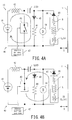
- a power supply section 40 in an eddy-current flaw detecting apparatus 10 of a fourth embodiment includes a DC power supply 41, a charging coil 42 and a changeover switch 43.
- this changeover switch 43 When this changeover switch 43 is placed in a first setting condition ( Fig. 4A ), a closed circuit is formed by the DC power supply 41, the charging coil 42 and a capacitor 12.
- this changeover switch 43 When this changeover switch 43 is placed in a second setting condition ( Fig. 4B ), a closed circuit is formed by the capacitor 12 and the coil section 20.
- constituent parts identical or corresponding to those of Fig. 1 are denoted by like reference numerals and characters and will not be discussed again here.
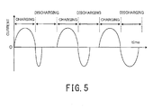
- Fig. 5 is a graph illustrating the waveform of a current caused to flow in the circuit by the operation of the power supply section 40 in the eddy-current flaw detecting apparatus 10 ( Fig. 4 ) of the fourth embodiment.
- a switch setting section 47 goes into a first setting condition ( Fig. 4A ) in each charging period shown in Fig. 5 and into a second setting condition ( Fig. 4B ) in each discharging period.
- a circuit composed of the DC power supply 41, the charging coil 42, the capacitor 12 and a resistor 44 is formed by the functions of diodes 45 and 46. Then, electrical charges are charged from the DC power supply 41 to the capacitor 12 at a response speed consistent with the time constant of this circuit.
- the switch setting section 47 switches over to the second setting condition shown in Fig. 4B , a circuit composed of the capacitor 12 and the coil section 20 is formed likewise by the functions of the diodes 45 and 46. Then, electrical charges charged in the capacitor 12 are discharged to the coil section 20 as an excitation current at a response speed consistent with the time constant of this circuit.
- an eddy-current flaw detecting apparatus 10 comprises a sensitivity correcting section 17 for correcting the sensitivity of a detecting section 14, and a phase difference detecting section 18 for detecting a phase difference between the output waveforms of a power supply section 13 and a detecting section 14, as the result of the power supply frequency f of the power supply section 13 or the electrostatic capacitance C of the capacitor 12 being made adjustable.
- a sensitivity correcting section 17 for correcting the sensitivity of a detecting section 14
- a phase difference detecting section 18 for detecting a phase difference between the output waveforms of a power supply section 13 and a detecting section 14, as the result of the power supply frequency f of the power supply section 13 or the electrostatic capacitance C of the capacitor 12 being made adjustable.
- the sensitivity of defect detection by a coil section 20 also varies.
- a relationship between the frequency f of the power supply section 13 and the sensitivity of defect detection by the coil section 20 is previously compiled into a database to determine the sensitivity correction coefficient of the detecting section 14 with relevant to the power supply frequency f.
- the sensitivity correcting section 17 feeds back a sensitivity correction coefficient corresponding to setting information on the power supply frequency f acquired from the adjustment section 30 to the detecting section 14, thereby always maintaining the defect detection sensitivity at a constant level.
- phase angle of the output waveform of the coil section 20 detected by the detecting section 14 also varies.
- the phase angle thus detected includes defect information attributable to defects and noise information attributable to a liftoff. Each piece of information varies differently with respect to a variation in the power supply frequency f.
- a first coil section 20a for generating an AC magnetic field whereby an eddy current is induced in an inspection object 11 and a second coil section 20b for detecting the magnetic field of the eddy current thus induced are separately formed in a coil section 20 of an eddy-current flaw detecting apparatus 10 according to a sixth embodiment.
- constituent parts identical or corresponding to those of Fig. 1 are denoted by like reference numerals and characters and will not be discussed again here.
- a remote-field eddy-current flaw detection apparatus or the like has a configuration corresponding to such a configuration as described above.
- a first resonance circuit 21 including the first coil section 20a is provided with a power supply section 13 and a first capacitor 12a.
- a second resonance circuit 22 including the second coil section 20b is provided with a detecting section 14 and a second capacitor 12b.
- the electrostatic capacitance C of the first capacitor 12a and the inductance L 1 + L 2 (x) of the first coil section 20a in the first resonance circuit 21 and the electrostatic capacitance C of the second capacitor 12b and the inductance L 1 + L 2 (x) of the second coil section 20b in the second resonance circuit 22 are set so that the resonance frequency f r shown by Equation (1) mentioned earlier equals the power supply frequency f.
- the electrostatic capacitances and the inductances are set so that the resonance frequencies of the first resonance circuit 21 and the second resonance circuit 22 are the same.
- Equation (1) the resonance conditions shown by Equation (1) mentioned earlier are satisfied in the first resonance circuit 21, and an excitation current supplied to the first coil section 20a is maximized.
- an eddy current induced by this excitation current is made larger and the strength of a magnetic field induced by this eddy current is made higher.
- Fig. 8A is a graph illustrating a change in the detection sensitivity of a coil section with the increase of a liftoff in a case where no resonance circuits are used.
- the detection sensitivity S decreases and noise N increases along with the increase of the liftoff x.
- Fig. 8B is a graph illustrating a change in the detection sensitivity of a coil section with the increase of a liftoff in a case where a resonance circuit having a fixed resonance frequency is used.
- the tendency of the detection sensitivity S to decrease and the noise N to increase along with the increase of the liftoff x is the same as the tendency in the case where no resonance circuits are used ( Fig. 8A ).
- the decrease of the S/N ratio is prevented accordingly.
- Fig. 8C is a graph illustrating a change in the detection sensitivity of a coil section with the increase of a liftoff in a case where a resonance circuit having a resonance frequency variable according to the liftoff is used.
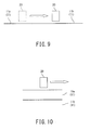
- Fig. 9 is a schematic view when an eddy-current flaw detecting apparatus according to each embodiment is applied to an inspection object 11 composed of a nonmagnetic substance 11a and a magnetic substance 11b.
- the resonance circuit of the apparatus is set so as to be in a resonant state while flaw detection is performed on a nonmagnetic substance 11a and so as to be out of a resonant state while flaw detection is performed on a magnetic substance 11b.
- the inductance of a coil greatly differs depending on whether the inspection object 11 is the nonmagnetic substance 11a or the magnetic substance 11b. Accordingly, if the power supply frequency f and the electrostatic capacitance C are adjusted so that the resonance circuit goes into a resonant state at the nonmagnetic substance 11 a, the resonance circuit automatically falls out of the resonant state when the apparatus is switched over to the magnetic substance 11b.
- the sensitivity of the coil section 20 increases due to the effects of the high magnetic permeability of the magnetic substance.
- This high magnetic permeability has a variation within the magnetic substance 11b, however, thus leading to high noise at the time of flaw detection.
- the resonance conditions of the circuit are satisfied to improve defect detection sensitivity.
- the resonance conditions of the circuit are not satisfied to reduce noise and improve defect detection sensitivity.
- Fig. 10 is a schematic view when an eddy-current flaw detecting apparatus 10 according to each embodiment is applied to an inspection object 11 composed of a nonmagnetic substance 11a and a magnetic substance 11b to perform flaw detection from the laminating direction thereof.
- An eddy-current flaw detecting apparatus 10 when applied to such an inspection object as illustrated in Fig. 10 to perform flaw detection with the nonmagnetic substance 11a, for example, as the object to be inspected, is configured so that a resonance circuit resonates with the nonmagnetic substance 11 a. Since the resonance circuit does not go into a resonant state for the magnetic substance 11b, sensitivity is improved only for the nonmagnetic substance 11 a. Consequently, noise resulting from the presence of the magnetic substance 11b is relatively suppressed.
- the positional relationship between the nonmagnetic substance 11a and the magnetic substance 11b may be reversed.
- Examples of such an inspection object include a structure welded or coated with a material different from a base material, and a location where a piping support overlaps with pipes being supported thereby.
- the inspection object 11 is composed of the nonmagnetic substance 11 a and the magnetic substance 11b.
- the inspection object may be composed of members different in magnetic permeability, rather than the nonmagnetic substance and the magnetic substance. Consequently, the same advantageous effect can be obtained by setting the apparatus so as to satisfy resonance conditions for either one of the members.
- the apparatus is set so as to satisfy resonance conditions for a member lower in magnetic permeability. If the apparatus is set so as to satisfy resonance conditions for a member higher in magnetic permeability, sensitivity is increased for the member having higher magnetic permeability. Consequently, it is possible to inspect, for example, a high-permeability member present in an area from the inner surface to the outer surface of a pipe (low in magnetic permeability).
- an eddy-current flaw detecting apparatus of at least one of the above-described embodiments, it is possible to prevent the decrease of defect detection sensitivity with the increase of a liftoff by including a capacitor for forming a resonance circuit along with a coil section. It is also possible to improve defect detection sensitivity without having to make the coil section (sensor head) larger.
Landscapes
- Chemical & Material Sciences (AREA)
- Chemical Kinetics & Catalysis (AREA)
- Electrochemistry (AREA)
- Physics & Mathematics (AREA)
- Health & Medical Sciences (AREA)
- Life Sciences & Earth Sciences (AREA)
- Analytical Chemistry (AREA)
- Biochemistry (AREA)
- General Health & Medical Sciences (AREA)
- General Physics & Mathematics (AREA)
- Immunology (AREA)
- Pathology (AREA)
- Investigating Or Analyzing Materials By The Use Of Magnetic Means (AREA)
Abstract
Description
- The present invention relates to an eddy-current flaw detection technique to detect defects, such as cracks, present in an inspection object.
- An eddy-current flaw detecting apparatus is used to detect cracks present in the vicinity of a metal surface of an inspection object. This apparatus generates an AC magnetic field by a coil section arranged on or above the metal surface to induce an eddy current in the vicinity of the metal surface by this AC magnetic field. If any cracks (defects) are present in the vicinity of the metal surface, the flow of the induced eddy current changes, thus also changing the strength distribution of the magnetic field induced by the eddy current.
- By detecting this change in the strength distribution of the induced magnetic field as a change in the output waveform of the arranged coil section, it is possible to detect the presence or absence of cracks.
- In this apparatus, if a distance (liftoff) between the surface and the coil section is made longer in a case, for example, where flaw detection is performed on an inspection object having a curved surface, the sensitivity of crack detection decreases and noise increases. The apparatus thus has the problem of the S/N ratio of an output waveform becoming lower.
- As a related art for solving such problems, there has been disclosed a technique to apply a ferrite core to a coil section to prevent the decrease of an S/N ratio associated with a liftoff (see, for example, Patent Document 1).
- Patent Document 1: Japanese Patent Laid-Open No.
2011-117872 - Such a method for preventing the decrease of an S/N ratio associated with the liftoff by contriving the structure or the material of the coil section as used in the above-described related art has had limitations if a curved surface or a circular tube having a smaller curvature radius is used as the inspection object. Since an even larger liftoff is anticipated in this case, there is a demand for the creation of a method for preventing the decrease of an S/N ratio which can be implemented along with the above-described method for contriving the structure or the material of the coil section and which works on other principles.
- The present invention has been accomplished in view of such circumstances as described above. Accordingly, an object of the present invention is to provide an eddy-current flaw detection technique to improve the S/N ratio of an output waveform of a coil section for detecting defects in an inspection object.
- An eddy-current flaw detecting apparatus comprises a power supply section for generating an AC magnetic field in a coil section to induce an eddy current in an inspection object; a detecting section for detecting an output waveform of the coil section to which an induced magnetic field of the eddy current is applied; and a capacitor for forming a resonance circuit along with the coil section.
- According to the present invention, there is provided an eddy-current flaw detection technique to improve the S/N ratio of an output waveform of a coil section for detecting cracks (defects) in an inspection object.
-
-
Fig. 1 is a circuit diagram illustrating a first embodiment of an eddy-current flaw detecting apparatus according to the present invention. -
Fig. 2A is a circuit diagram illustrating a second embodiment of the eddy-current flaw detecting apparatus according to the present invention, whereasFig. 2B is a graph illustrating a relationship between the power supply frequency of a power supply section and an excitation current flowing in the circuit of the apparatus. -
Fig. 3A is a circuit diagram illustrating a third embodiment of the eddy-current flaw detecting apparatus according to the present invention, whereasFig. 3B is a circuit diagram illustrating a modified example of the capacitor. -
Fig. 4A is a circuit diagram illustrating a changeover switch in a first setting condition in a fourth embodiment of the eddy-current flaw detecting apparatus according to the present invention, whereasFig. 4B is a circuit diagram illustrating the changeover switch in a second setting condition. -
Fig. 5 is a graph illustrating the waveform of a current caused to flow in the circuit by the operation of the power supply section in the fourth embodiment of the eddy-current flaw detecting apparatus. -
Fig. 6 is a circuit diagram illustrating a fifth embodiment of the eddy-current flaw detecting apparatus according to the present invention. -
Fig. 7 is a circuit diagram illustrating a sixth embodiment of the eddy-current flaw detecting apparatus according to the present invention. -
Fig. 8A is a graph illustrating a change in the detection sensitivity of a coil section with the increase of a liftoff in a case where no resonance circuits are used, whereasFig. 8B is a graph illustrating a change in the detection sensitivity of a coil section with the increase of a liftoff in a case where the resonance frequency of a resonance circuit is fixed, andFig. 8C is a graph illustrating a change in the detection sensitivity of a coil section with the increase of a liftoff in a case where the resonance frequency of a resonance circuit is varied in correspondence with a liftoff. -
Fig. 9 is a schematic view when an eddy-current flaw detecting apparatus according to each embodiment is applied to an inspection object composed of a nonmagnetic substance and a magnetic substance. -
Fig. 10 is a schematic view when an eddy-current flaw detecting apparatus according to each embodiment is applied to an inspection object composed of a nonmagnetic substance and a magnetic substance stacked on each other. - Hereinafter, embodiments of the present invention will be described according to the accompanying drawings.
- As illustrated in
Fig. 1 , an eddy-currentflaw detecting apparatus 10 according to a first embodiment comprises apower supply section 13 for generating an AC magnetic field in acoil section 20 to induce an eddy current in aninspection object 11; a detectingsection 14 for detecting an output waveform of thecoil section 20 to which an induced magnetic field of the eddy current is applied; and acapacitor 12 for forming a resonance circuit along with thecoil section 20. - The circuit of the eddy-current
flaw detecting apparatus 10 is formed of thepower supply section 13 for providing an AC voltage having a frequency f, thecapacitor 12 having an electrostatic capacitance C, and thecoil section 20. Thecoil section 20 features an internal resistance R, an intrinsic inductance L1 of a coil, and a variable inductance L2(x) dependent on a liftoff x. - When the AC voltage having the frequency f is applied to the circuit by the
power supply section 13, an excitation current of the same frequency f is supplied to thecoil section 20. Then, the circuit goes into a resonant state under the condition of the frequency f (= fr) of thepower supply section 13 satisfying Equation (1) shown below. The excitation current flowing in the circuit thus takes a local maximum value (seeFig. 2B ).
- When the excitation current is supplied to the
coil section 20, an AC magnetic field is generated within and around the coil section. An eddy current is induced in the vicinity of a surface of theinspection object 11 by this AC magnetic field. Under this condition, the surface of theinspection object 11 is scanned with thecoil section 20. Consequently, the flow of the induced eddy current changes at a point where a defect, such as a crack, is present, thus changing the strength distribution of a magnetic field induced by this eddy current. - This change in the magnetic field strength distribution is received by the
coil section 20 and a change in the output waveform of thecoil section 20 is detected at the detectingsection 14, thereby detecting the presence or absence of cracks. - The excitation current supplied to the
coil section 20 is maximum in a case where the settings of thepower supply section 13, thecapacitor 12 and thecoil section 20 satisfy resonance conditions shown by Equation (1) mentioned above. This also maximizes the strength of an AC magnetic field generated by this excitation current, an eddy current induced by this AC magnetic field, and the strength of a magnetic field induced by this eddy current. When the magnetic field induced by this eddy current is applied to thecoil section 20, only the frequency component of the magnetic field corresponding to the power supply frequency f is selectively detected on the basis of the resonance characteristics of the circuit. This selective detection improves the S/N ratio of an output waveform of the detectingsection 14 and the sensitivity of detection of defects, such as cracks. - Accordingly, the decrease of defect detection sensitivity is prevented even if a liftoff x large in value to some extent is present between the
coil section 20 and theinspection object 11, as long as the resonance conditions (Equation (1)) are satisfied. - The
inspection object 11 to which an eddy-currentflaw detecting apparatus 10 according to an embodiment is applied is preferably a pipe or a curved surface which is small in curvature radius and the liftoff x of which is therefore unavoidably large. The eddy-currentflaw detecting apparatus 10 is also applicable to a flat surface without difficulty, however. - There can be mentioned various ways (not illustrated) of scanning a surface of the
inspection object 11 with thecoil section 20. For example, scanning can be achieved by means of a wheeled dolly, traction with a wire, or extrusion using a pressure gas. - Although the circuit comprises an LC series circuit in each embodiment, the circuit may be formed of an LC parallel circuit as long as the LC parallel circuit is configured to place the circuit in a resonant state.
- As illustrated in
Fig. 2A , an eddy-currentflaw detecting apparatus 10 of a second embodiment comprises an excitation current monitor 15 for monitoring an excitation current caused to flow in the circuit (coil section 20) by the operation of thepower supply section 13; and afrequency adjusting section 30a (adjustment section 30) for adjusting the power supply frequency f of thepower supply section 13, so that the circuit goes into a resonant state. Note that inFig. 2A , constituent parts identical or corresponding to those ofFig. 1 are denoted by like reference numerals and characters and will not be discussed again here. -
Fig. 2B is a graph illustrating a relationship between the power supply frequency f of thepower supply section 13 and an excitation current flowing in the circuit. - As shown by a solid line in this graph, an excitation current supplied to the
coil section 20 takes a maximum value as long as an AC voltage having an AC voltage resonance frequency of fr(x1) satisfying Equation (1) mentioned above is applied by thepower supply section 13 under the premise that a liftoff X1 is constant. An eddy current induced in theinspection object 11 is also maximized, thus causing the output waveform of the detectingsection 14 to be also maximum in strength. Consequently, the defect detection sensitivity of theinspection object 11 is maximum. - However, if a distance between a surface of the
inspection object 11 and thecoil section 20 for scanning the object varies and the liftoff therefore changes to x2, the variable inductance L2 also changes, thus causing the distribution of the excitation current to shift as shown by a dashed line. - In cases where the excitation current distribution is shown in this way by the dashed line, the circuit falls out of a resonant state if the AC voltage of the
power supply section 13 remains at a resonance frequency of fr(x1). Consequently, the excitation current supplied to thecoil section 20 decreases, and therefore, the defect detection sensitivity of theinspection object 11 decreases as well. - Accordingly, the resonance frequency of the AC voltage of the
power supply section 13 is changed to fr(x2) to maintain the resonant state of the circuit, thereby maintaining the defect detection sensitivity of theinspection object 11 at a maximum level. - As illustrated in
Fig. 3A , an eddy-currentflaw detecting apparatus 10 of a third embodiment comprises an electrostaticcapacitance adjusting section 30b (adjustment section 30) for adjusting the electrostatic capacitance C of acapacitor 12, so that the circuit of the apparatus goes into a resonant state. Note that inFig. 3A , constituent parts identical or corresponding to those ofFig. 1 are denoted by like reference numerals and characters and will not be discussed again here. - In the third embodiment, the electrostatic capacitance C of the
capacitor 12 is adjusted to satisfy Equation (1) if the liftoff x changes. This apparatus configuration maintains the resonant state of the circuit, thereby maintaining the defect detection sensitivity of theinspection object 11 at a maximum level. -
Fig. 3B is a circuit diagram illustrating a modified example of thecapacitor 12. - The
capacitor 12 illustrated inFig. 3A is configured to adjust the electrostatic capacitance C in a continuous manner (adjusted by, for example, making a distance between electrode plates constituting thecapacitor 12 variable using a motor and a gear). In thecapacitor 12 illustrated inFig. 3B , a plurality (three in the figure) of capacitors 33 (33a, 33b and 33c) is selectively switched over with aswitch 32 to adjust the electrostatic capacitance C in a stepwise manner. - Note that the adjustment section 30 (30a and 30b) can adjust the power supply frequency f and the electrostatic capacitance C according to not only the excitation current monitor 15 but also the output of the detecting
section 14. - As illustrated in
Fig. 4 , apower supply section 40 in an eddy-currentflaw detecting apparatus 10 of a fourth embodiment includes aDC power supply 41, a chargingcoil 42 and achangeover switch 43. When thischangeover switch 43 is placed in a first setting condition (Fig. 4A ), a closed circuit is formed by theDC power supply 41, the chargingcoil 42 and acapacitor 12. When thischangeover switch 43 is placed in a second setting condition (Fig. 4B ), a closed circuit is formed by thecapacitor 12 and thecoil section 20. Note that inFig. 4 , constituent parts identical or corresponding to those ofFig. 1 are denoted by like reference numerals and characters and will not be discussed again here. -
Fig. 5 is a graph illustrating the waveform of a current caused to flow in the circuit by the operation of thepower supply section 40 in the eddy-current flaw detecting apparatus 10 (Fig. 4 ) of the fourth embodiment. - A
switch setting section 47 goes into a first setting condition (Fig. 4A ) in each charging period shown inFig. 5 and into a second setting condition (Fig. 4B ) in each discharging period. - In the first setting condition shown in
Fig. 4A , a circuit composed of theDC power supply 41, the chargingcoil 42, thecapacitor 12 and aresistor 44 is formed by the functions ofdiodes DC power supply 41 to thecapacitor 12 at a response speed consistent with the time constant of this circuit. - At a point where this charging is completed, the
switch setting section 47 switches over to the second setting condition shown inFig. 4B , a circuit composed of thecapacitor 12 and thecoil section 20 is formed likewise by the functions of thediodes capacitor 12 are discharged to thecoil section 20 as an excitation current at a response speed consistent with the time constant of this circuit. - In cases where electrical charges charged to the
capacitor 12 are discharged to thecoil section 20 as described above, the resonance conditions of the circuit are always satisfied even if the liftoff x changes. - Accordingly, there is no need to control the frequency f of the
power supply section 40 or the electrostatic capacitance C of thecapacitor 12 in the fourth embodiment. The configuration of the apparatus can therefore be simplified. - As illustrated in
Fig. 6 , an eddy-currentflaw detecting apparatus 10 according to a fifth embodiment comprises asensitivity correcting section 17 for correcting the sensitivity of a detectingsection 14, and a phasedifference detecting section 18 for detecting a phase difference between the output waveforms of apower supply section 13 and a detectingsection 14, as the result of the power supply frequency f of thepower supply section 13 or the electrostatic capacitance C of thecapacitor 12 being made adjustable. Note that inFig. 6 , constituent parts identical or corresponding to those ofFig. 1 are denoted by like reference numerals and characters and will not be discussed again here. - When the frequency f of the
power supply section 13 is varied by anadjustment section 30, the sensitivity of defect detection by acoil section 20 also varies. Hence, a relationship between the frequency f of thepower supply section 13 and the sensitivity of defect detection by thecoil section 20 is previously compiled into a database to determine the sensitivity correction coefficient of the detectingsection 14 with relevant to the power supply frequency f. Then, thesensitivity correcting section 17 feeds back a sensitivity correction coefficient corresponding to setting information on the power supply frequency f acquired from theadjustment section 30 to the detectingsection 14, thereby always maintaining the defect detection sensitivity at a constant level. - When the power supply frequency f is varied, the phase angle of the output waveform of the
coil section 20 detected by the detectingsection 14 also varies. The phase angle thus detected includes defect information attributable to defects and noise information attributable to a liftoff. Each piece of information varies differently with respect to a variation in the power supply frequency f. - By comparing the variation of the power supply frequency f and the variation of phase angle information in the phase
difference detecting section 18, it is possible to determine whether the information acquired by the detectingsection 14 is attributable to defects or noise. - As illustrated in
Fig. 7 , afirst coil section 20a for generating an AC magnetic field whereby an eddy current is induced in aninspection object 11 and asecond coil section 20b for detecting the magnetic field of the eddy current thus induced are separately formed in acoil section 20 of an eddy-currentflaw detecting apparatus 10 according to a sixth embodiment. Note that inFig. 7 , constituent parts identical or corresponding to those ofFig. 1 are denoted by like reference numerals and characters and will not be discussed again here. - Here, a positional relationship between the
first coil section 20a and thesecond coil section 20b is fixed, and a surface of theinspection object 11 is scanned with both coil sections in a unified manner. A remote-field eddy-current flaw detection apparatus or the like has a configuration corresponding to such a configuration as described above. - A
first resonance circuit 21 including thefirst coil section 20a is provided with apower supply section 13 and afirst capacitor 12a. Asecond resonance circuit 22 including thesecond coil section 20b is provided with a detectingsection 14 and asecond capacitor 12b. - In the sixth embodiment, the electrostatic capacitance C of the
first capacitor 12a and the inductance L1 + L2(x) of thefirst coil section 20a in thefirst resonance circuit 21 and the electrostatic capacitance C of thesecond capacitor 12b and the inductance L1 + L2(x) of thesecond coil section 20b in thesecond resonance circuit 22 are set so that the resonance frequency fr shown by Equation (1) mentioned earlier equals the power supply frequency f. In other words, the electrostatic capacitances and the inductances are set so that the resonance frequencies of thefirst resonance circuit 21 and thesecond resonance circuit 22 are the same. - Consequently, the resonance conditions shown by Equation (1) mentioned earlier are satisfied in the
first resonance circuit 21, and an excitation current supplied to thefirst coil section 20a is maximized. In addition, an eddy current induced by this excitation current is made larger and the strength of a magnetic field induced by this eddy current is made higher. - When the magnetic field induced by this eddy current is applied to the
second coil section 20b, only the frequency component of the magnetic field corresponding to the power supply frequency f is selectively detected on the basis of the resonance characteristics of thesecond resonance circuit 22. This selective detection improves the S/N ratio of an output waveform of the detectingsection 14 and the sensitivity of detection of defects, such as cracks. - The principle that an S/N ratio improves and the sensitivity of detection of defects, such as cracks, increases in each embodiment will be described with reference to
Fig. 8 . -
Fig. 8A is a graph illustrating a change in the detection sensitivity of a coil section with the increase of a liftoff in a case where no resonance circuits are used. - In general, the eddy-current
flaw detecting apparatus 10 is tuned so that detection sensitivity S is maximum at a point where liftoff x = 0. As conceptually illustratedFig. 8A , the detection sensitivity S decreases and noise N increases along with the increase of the liftoff x. -
Fig. 8B is a graph illustrating a change in the detection sensitivity of a coil section with the increase of a liftoff in a case where a resonance circuit having a fixed resonance frequency is used. - In this case, the tendency of the detection sensitivity S to decrease and the noise N to increase along with the increase of the liftoff x is the same as the tendency in the case where no resonance circuits are used (
Fig. 8A ). Initial sensitivity (sensitivity at a point where liftoff x = 0) is made higher by the use of the resonance circuit, however, and the decrease of the S/N ratio is prevented accordingly. -
Fig. 8C is a graph illustrating a change in the detection sensitivity of a coil section with the increase of a liftoff in a case where a resonance circuit having a resonance frequency variable according to the liftoff is used. - In this case, the increase of the noise N with the increase of the liftoff x is prevented, in addition to the initial sensitivity being improved. Consequently, an excellent S/N ratio can be obtained even if the liftoff is large.
-
Fig. 9 is a schematic view when an eddy-current flaw detecting apparatus according to each embodiment is applied to aninspection object 11 composed of anonmagnetic substance 11a and amagnetic substance 11b. - The resonance circuit of the apparatus is set so as to be in a resonant state while flaw detection is performed on a
nonmagnetic substance 11a and so as to be out of a resonant state while flaw detection is performed on amagnetic substance 11b. - Note that the inductance of a coil greatly differs depending on whether the
inspection object 11 is thenonmagnetic substance 11a or themagnetic substance 11b. Accordingly, if the power supply frequency f and the electrostatic capacitance C are adjusted so that the resonance circuit goes into a resonant state at thenonmagnetic substance 11 a, the resonance circuit automatically falls out of the resonant state when the apparatus is switched over to themagnetic substance 11b. - In general, when flaw detection is performed on a surface of the
magnetic substance 11b, the sensitivity of thecoil section 20 increases due to the effects of the high magnetic permeability of the magnetic substance. This high magnetic permeability has a variation within themagnetic substance 11b, however, thus leading to high noise at the time of flaw detection. - Accordingly, when flaw detection is performed on a surface of the
nonmagnetic substance 11 a, the resonance conditions of the circuit are satisfied to improve defect detection sensitivity. When flaw detection is performed on a surface of themagnetic substance 11b, the resonance conditions of the circuit are not satisfied to reduce noise and improve defect detection sensitivity. -
Fig. 10 is a schematic view when an eddy-currentflaw detecting apparatus 10 according to each embodiment is applied to aninspection object 11 composed of anonmagnetic substance 11a and amagnetic substance 11b to perform flaw detection from the laminating direction thereof. - An eddy-current
flaw detecting apparatus 10 according to each embodiment, when applied to such an inspection object as illustrated inFig. 10 to perform flaw detection with thenonmagnetic substance 11a, for example, as the object to be inspected, is configured so that a resonance circuit resonates with thenonmagnetic substance 11 a. Since the resonance circuit does not go into a resonant state for themagnetic substance 11b, sensitivity is improved only for thenonmagnetic substance 11 a. Consequently, noise resulting from the presence of themagnetic substance 11b is relatively suppressed. - Although a description has been made of an arrangement in which the
nonmagnetic substance 11 a is opposed to the eddy-currentflaw detecting apparatus 10, the positional relationship between thenonmagnetic substance 11a and themagnetic substance 11b may be reversed. Examples of such an inspection object include a structure welded or coated with a material different from a base material, and a location where a piping support overlaps with pipes being supported thereby. - Note that in the sixth and seventh embodiments, a description has been made on the premise that the
inspection object 11 is composed of thenonmagnetic substance 11 a and themagnetic substance 11b. However, the inspection object may be composed of members different in magnetic permeability, rather than the nonmagnetic substance and the magnetic substance. Consequently, the same advantageous effect can be obtained by setting the apparatus so as to satisfy resonance conditions for either one of the members. - In particular, a significant advantageous effect can be obtained if the apparatus is set so as to satisfy resonance conditions for a member lower in magnetic permeability. If the apparatus is set so as to satisfy resonance conditions for a member higher in magnetic permeability, sensitivity is increased for the member having higher magnetic permeability. Consequently, it is possible to inspect, for example, a high-permeability member present in an area from the inner surface to the outer surface of a pipe (low in magnetic permeability).
- According to an eddy-current flaw detecting apparatus of at least one of the above-described embodiments, it is possible to prevent the decrease of defect detection sensitivity with the increase of a liftoff by including a capacitor for forming a resonance circuit along with a coil section. It is also possible to improve defect detection sensitivity without having to make the coil section (sensor head) larger.
- While several embodiments of the present invention have been described, these embodiments are shown by way of example only and are not intended to limit the scope of the invention. These embodiments may be carried out in other various ways, and various omissions, substitutions and modifications may be made therein without departing from the gist of the invention. It should therefore be noted that these embodiments and the modifications thereof fall within the scope or gist of the invention, as well as in the scope of the present invention as defined by the appended claims and equivalents thereof.
- For example, it is possible to concomitantly use the configuration described in the second embodiment in which the electrostatic capacitance of the capacitor is adjusted in a continuous manner and the configuration described in the third embodiment in which the electrostatic capacitance of the capacitor is adjusted in a stepwise manner.
- 10...eddy-current flaw detecting apparatus, 11...inspection object, 11a...nonmagnetic substance, 11b...magnetic substance, 12...capacitor, 12a...first capacitor, 12b...second capacitor, 13...power supply section, 40...power supply section, 14...detecting section, 15...excitation current monitor, 17...sensitivity correcting section, 18...phase difference detecting section, 20...coil section, 20a...first coil section, 20b...second coil section, 21...first resonance circuit, 22...second resonance circuit, 30a(30)...frequency adjusting section, 30b(30)...electrostatic capacitance adjusting section, 32...switch, 33...capacitors, 41...DC power supply, 42...charging coil, 43...changeover switch, 44...resistor, 45...diodes, 46...diodes, 47...switch setting section, C...electrostatic capacitance, f...power supply frequency, L1...intrinsic inductance of a coil, L2(x)...variable inductance, L2(x)...dependent on a liftoff.
Claims (6)
- An eddy-current flaw detecting apparatus comprising:a power supply section for generating an AC magnetic field in a first coil section to induce an eddy current in an inspection object;a second coil section for detecting an induced magnetic field of the eddy current;a detecting section for detecting an output waveform of the second coil section;a first capacitor for forming a first resonance circuit along with the first coil section;a second capacitor for forming a second resonance circuit along with the second coil section; andan adjustment section for adjusting at least one of a power supply frequency of the power supply section, an electrostatic capacitance of the first capacitor and an electrostatic capacitance of the second capacitor, so as to place the first resonance circuit and the second resonance circuit in a resonant state at a same frequency.
- The eddy-current flaw detecting apparatus according to claim 1, wherein the power supply section includes a DC power supply, a charging coil and a changeover switch, thereby forming a closed circuit with the DC power supply, the charging coil and the first capacitor when the changeover switch goes into a first setting condition, and forming a closed circuit with the first capacitor and the first coil section when the changeover switch goes into a second setting condition.
- The eddy-current flaw detecting apparatus according to claim 1 or 2, comprising a sensitivity correcting section for correcting a sensitivity of the detecting section, as a result of at least one of the power supply frequency, the electrostatic capacitance of the first capacitor and the electrostatic capacitance of the second capacitor being made adjustable.
- The eddy-current flaw detecting apparatus according to any one of claims 1 to 3, comprising a phase difference detecting section for detecting a phase difference between the output waveforms of the power supply section and the detecting section.
- A method of eddy-current flaw detection using an eddy-current flaw detecting apparatus according to any one of claims 1 to 4, wherein the inspection object includes a first member and a second member different in magnetic permeability from the first member, and the first and second resonance circuits are set so as to be in a resonant state while flaw detection is performed on the first member and so as to be out of a resonant state while flaw detection is performed on the second member.
- The method of eddy-current flaw detection according to claim 5, wherein the first member is a nonmagnetic substance and the second member is a magnetic substance.
Applications Claiming Priority (2)
| Application Number | Priority Date | Filing Date | Title |
|---|---|---|---|
| JP2011209572 | 2011-09-26 | ||
| PCT/JP2012/074563 WO2013047521A1 (en) | 2011-09-26 | 2012-09-25 | Eddy current flaw detector and eddy current flaw detection method |
Publications (3)
| Publication Number | Publication Date |
|---|---|
| EP2762875A1 true EP2762875A1 (en) | 2014-08-06 |
| EP2762875A4 EP2762875A4 (en) | 2015-06-17 |
| EP2762875B1 EP2762875B1 (en) | 2019-07-17 |
Family
ID=47995553
Family Applications (1)
| Application Number | Title | Priority Date | Filing Date |
|---|---|---|---|
| EP12837050.9A Not-in-force EP2762875B1 (en) | 2011-09-26 | 2012-09-25 | Eddy current flaw detector |
Country Status (3)
| Country | Link |
|---|---|
| EP (1) | EP2762875B1 (en) |
| JP (1) | JP5931889B2 (en) |
| WO (1) | WO2013047521A1 (en) |
Cited By (2)
| Publication number | Priority date | Publication date | Assignee | Title |
|---|---|---|---|---|
| CN105092697A (en) * | 2015-07-13 | 2015-11-25 | 上海兰宝传感科技股份有限公司 | Metal detection system based on free damped oscillation technology and detection method |
| TWI794764B (en) * | 2021-03-05 | 2023-03-01 | 國立臺灣大學 | Eddy current sensing system and method thereof |
Families Citing this family (7)
| Publication number | Priority date | Publication date | Assignee | Title |
|---|---|---|---|---|
| JP6659527B2 (en) * | 2016-12-14 | 2020-03-04 | 株式会社東芝 | Apparatus and method for evaluating physical properties |
| JP7132873B2 (en) * | 2019-02-27 | 2022-09-07 | 公益財団法人鉄道総合技術研究所 | Braking device and braking method |
| JP2020197479A (en) * | 2019-06-04 | 2020-12-10 | 国立研究開発法人物質・材料研究機構 | Compact ultrasensitive magnetic impedance sensor and nondestructive inspection device using the same |
| JP6860715B2 (en) * | 2020-02-05 | 2021-04-21 | 株式会社東芝 | Physical property value evaluation device and method |
| ES2991833T3 (en) * | 2020-12-11 | 2024-12-05 | Abb Schweiz Ag | Pulsed eddy current system |
| CN113433211B (en) * | 2021-06-02 | 2025-04-15 | 爱德森(厦门)电子有限公司 | An online monitoring device for electrochemical protective layer and system method thereof |
| ES2984411T3 (en) * | 2021-07-07 | 2024-10-29 | Abb Schweiz Ag | Receiver for a pulsed eddy current system |
Family Cites Families (11)
| Publication number | Priority date | Publication date | Assignee | Title |
|---|---|---|---|---|
| US573182A (en) * | 1896-12-15 | Half to james h | ||
| US2329812A (en) * | 1941-12-05 | 1943-09-21 | Magnetic Analysis Corp | Electromagnetic inspection with alternating current |
| GB573182A (en) * | 1943-05-21 | 1945-11-09 | Arthur John King | Improvements in or relating to the detection of faults in articles of non-magnetic material |
| GB1503332A (en) * | 1974-02-11 | 1978-03-08 | Magnetic Analysis Corp | Eddy current testing apparatus |
| JPH09325132A (en) * | 1996-06-03 | 1997-12-16 | Daido Steel Co Ltd | Eddy current flaw detection device and eddy current flaw detection method |
| JP4006816B2 (en) * | 1998-03-09 | 2007-11-14 | 大同特殊鋼株式会社 | Eddy current flaw detector |
| JP2006053053A (en) * | 2004-08-12 | 2006-02-23 | Hide Imai | Eddy current flaw detection probe device |
| JP4872388B2 (en) * | 2006-03-10 | 2012-02-08 | 住友電気工業株式会社 | Eddy current flaw detection apparatus and eddy current flaw detection method for magnesium alloy |
| US7911205B2 (en) * | 2007-09-25 | 2011-03-22 | General Electric Company | Electromagnetic resonance frequency inspection systems and methods |
| JP4863127B2 (en) * | 2008-05-15 | 2012-01-25 | 住友金属工業株式会社 | Magnetic flaw detection method and magnetic flaw detection apparatus |
| JP5203342B2 (en) | 2009-12-04 | 2013-06-05 | 株式会社東芝 | Eddy current flaw detection probe and eddy current flaw detection test apparatus using the same |
-
2012
- 2012-09-25 WO PCT/JP2012/074563 patent/WO2013047521A1/en not_active Ceased
- 2012-09-25 JP JP2013536301A patent/JP5931889B2/en not_active Expired - Fee Related
- 2012-09-25 EP EP12837050.9A patent/EP2762875B1/en not_active Not-in-force
Cited By (3)
| Publication number | Priority date | Publication date | Assignee | Title |
|---|---|---|---|---|
| CN105092697A (en) * | 2015-07-13 | 2015-11-25 | 上海兰宝传感科技股份有限公司 | Metal detection system based on free damped oscillation technology and detection method |
| CN105092697B (en) * | 2015-07-13 | 2018-06-26 | 上海兰宝传感科技股份有限公司 | Metal detection system and detection method based on free damping oscillation technology |
| TWI794764B (en) * | 2021-03-05 | 2023-03-01 | 國立臺灣大學 | Eddy current sensing system and method thereof |
Also Published As
| Publication number | Publication date |
|---|---|
| WO2013047521A1 (en) | 2013-04-04 |
| JPWO2013047521A1 (en) | 2015-03-26 |
| EP2762875B1 (en) | 2019-07-17 |
| JP5931889B2 (en) | 2016-06-08 |
| EP2762875A4 (en) | 2015-06-17 |
Similar Documents
| Publication | Publication Date | Title |
|---|---|---|
| EP2762875B1 (en) | Eddy current flaw detector | |
| CN107529346B (en) | Inductive Power Transmitter | |
| JP6768486B2 (en) | Rail inspection system | |
| EP0884588B1 (en) | Eddy current flaw detector | |
| CN106441378B (en) | Eddy current sensor and material gear adjusting resistance determining method and testing method thereof | |
| CN105891323A (en) | Eddy probe array for detecting pipeline deformation | |
| CN105431321B (en) | Object detecting system and the method for operating object detecting system | |
| US20140091785A1 (en) | Target clearance measurement device | |
| CN113029879B (en) | Method for multi-frequency on-line monitoring of metal particles in oil and detection device thereof | |
| US20130076373A1 (en) | Target sensor | |
| KR20150048141A (en) | Eddy current flaw detection probe and eddy current flaw inspection apparatus | |
| Kim et al. | Eddy current probes of inclined coils for increased detectability of circumferential cracks in tubing | |
| CN107764346B (en) | Method for operating a magnetic-inductive flow meter and magnetic-inductive flow meter | |
| US20120206133A1 (en) | Resonant Electromagnetic Sensor | |
| CN120668771B (en) | Method for detecting cracks in any direction in carbon steel based on magnetic resistance disturbance | |
| CN102176060A (en) | Inductance approach switch sensor | |
| CN107681942A (en) | The reduction fluctuated using the motor torque of the total line harmonics of DC | |
| JP6601226B2 (en) | Magnetic flux leakage flaw detector | |
| CN203191354U (en) | Eddy current flaw detector | |
| JP4192708B2 (en) | Magnetic sensor | |
| CN103940860B (en) | A kind of method of series resonant circuit capacitance detecting nonmetallic materials discontinuity | |
| JP2003050234A (en) | Eddy-current flaw detection testing device | |
| CN117630160A (en) | Industrial quality inspection metal detection device and method | |
| CN103940859B (en) | A kind of method of antiresonant circuit capacitance detecting nonmetallic materials discontinuity | |
| JP2012026806A (en) | Remote field eddy current flow detector, and method |
Legal Events
| Date | Code | Title | Description |
|---|---|---|---|
| PUAI | Public reference made under article 153(3) epc to a published international application that has entered the european phase |
Free format text: ORIGINAL CODE: 0009012 |
|
| 17P | Request for examination filed |
Effective date: 20140326 |
|
| AK | Designated contracting states |
Kind code of ref document: A1 Designated state(s): AL AT BE BG CH CY CZ DE DK EE ES FI FR GB GR HR HU IE IS IT LI LT LU LV MC MK MT NL NO PL PT RO RS SE SI SK SM TR |
|
| DAX | Request for extension of the european patent (deleted) | ||
| RA4 | Supplementary search report drawn up and despatched (corrected) |
Effective date: 20150519 |
|
| RIC1 | Information provided on ipc code assigned before grant |
Ipc: G01N 27/90 20060101AFI20150512BHEP |
|
| STAA | Information on the status of an ep patent application or granted ep patent |
Free format text: STATUS: EXAMINATION IS IN PROGRESS |
|
| 17Q | First examination report despatched |
Effective date: 20171117 |
|
| GRAP | Despatch of communication of intention to grant a patent |
Free format text: ORIGINAL CODE: EPIDOSNIGR1 |
|
| STAA | Information on the status of an ep patent application or granted ep patent |
Free format text: STATUS: GRANT OF PATENT IS INTENDED |
|
| INTG | Intention to grant announced |
Effective date: 20190307 |
|
| GRAS | Grant fee paid |
Free format text: ORIGINAL CODE: EPIDOSNIGR3 |
|
| GRAA | (expected) grant |
Free format text: ORIGINAL CODE: 0009210 |
|
| STAA | Information on the status of an ep patent application or granted ep patent |
Free format text: STATUS: THE PATENT HAS BEEN GRANTED |
|
| AK | Designated contracting states |
Kind code of ref document: B1 Designated state(s): AL AT BE BG CH CY CZ DE DK EE ES FI FR GB GR HR HU IE IS IT LI LT LU LV MC MK MT NL NO PL PT RO RS SE SI SK SM TR |
|
| REG | Reference to a national code |
Ref country code: GB Ref legal event code: FG4D |
|
| REG | Reference to a national code |
Ref country code: CH Ref legal event code: EP |
|
| REG | Reference to a national code |
Ref country code: IE Ref legal event code: FG4D |
|
| REG | Reference to a national code |
Ref country code: DE Ref legal event code: R096 Ref document number: 602012062152 Country of ref document: DE |
|
| REG | Reference to a national code |
Ref country code: AT Ref legal event code: REF Ref document number: 1156313 Country of ref document: AT Kind code of ref document: T Effective date: 20190815 |
|
| REG | Reference to a national code |
Ref country code: NL Ref legal event code: MP Effective date: 20190717 |
|
| REG | Reference to a national code |
Ref country code: LT Ref legal event code: MG4D |
|
| REG | Reference to a national code |
Ref country code: AT Ref legal event code: MK05 Ref document number: 1156313 Country of ref document: AT Kind code of ref document: T Effective date: 20190717 |
|
| PG25 | Lapsed in a contracting state [announced via postgrant information from national office to epo] |
Ref country code: HR Free format text: LAPSE BECAUSE OF FAILURE TO SUBMIT A TRANSLATION OF THE DESCRIPTION OR TO PAY THE FEE WITHIN THE PRESCRIBED TIME-LIMIT Effective date: 20190717 Ref country code: PT Free format text: LAPSE BECAUSE OF FAILURE TO SUBMIT A TRANSLATION OF THE DESCRIPTION OR TO PAY THE FEE WITHIN THE PRESCRIBED TIME-LIMIT Effective date: 20191118 Ref country code: NL Free format text: LAPSE BECAUSE OF FAILURE TO SUBMIT A TRANSLATION OF THE DESCRIPTION OR TO PAY THE FEE WITHIN THE PRESCRIBED TIME-LIMIT Effective date: 20190717 Ref country code: FI Free format text: LAPSE BECAUSE OF FAILURE TO SUBMIT A TRANSLATION OF THE DESCRIPTION OR TO PAY THE FEE WITHIN THE PRESCRIBED TIME-LIMIT Effective date: 20190717 Ref country code: LT Free format text: LAPSE BECAUSE OF FAILURE TO SUBMIT A TRANSLATION OF THE DESCRIPTION OR TO PAY THE FEE WITHIN THE PRESCRIBED TIME-LIMIT Effective date: 20190717 Ref country code: BG Free format text: LAPSE BECAUSE OF FAILURE TO SUBMIT A TRANSLATION OF THE DESCRIPTION OR TO PAY THE FEE WITHIN THE PRESCRIBED TIME-LIMIT Effective date: 20191017 Ref country code: NO Free format text: LAPSE BECAUSE OF FAILURE TO SUBMIT A TRANSLATION OF THE DESCRIPTION OR TO PAY THE FEE WITHIN THE PRESCRIBED TIME-LIMIT Effective date: 20191017 Ref country code: AT Free format text: LAPSE BECAUSE OF FAILURE TO SUBMIT A TRANSLATION OF THE DESCRIPTION OR TO PAY THE FEE WITHIN THE PRESCRIBED TIME-LIMIT Effective date: 20190717 Ref country code: SE Free format text: LAPSE BECAUSE OF FAILURE TO SUBMIT A TRANSLATION OF THE DESCRIPTION OR TO PAY THE FEE WITHIN THE PRESCRIBED TIME-LIMIT Effective date: 20190717 |
|
| PG25 | Lapsed in a contracting state [announced via postgrant information from national office to epo] |
Ref country code: IS Free format text: LAPSE BECAUSE OF FAILURE TO SUBMIT A TRANSLATION OF THE DESCRIPTION OR TO PAY THE FEE WITHIN THE PRESCRIBED TIME-LIMIT Effective date: 20191117 Ref country code: RS Free format text: LAPSE BECAUSE OF FAILURE TO SUBMIT A TRANSLATION OF THE DESCRIPTION OR TO PAY THE FEE WITHIN THE PRESCRIBED TIME-LIMIT Effective date: 20190717 Ref country code: LV Free format text: LAPSE BECAUSE OF FAILURE TO SUBMIT A TRANSLATION OF THE DESCRIPTION OR TO PAY THE FEE WITHIN THE PRESCRIBED TIME-LIMIT Effective date: 20190717 Ref country code: GR Free format text: LAPSE BECAUSE OF FAILURE TO SUBMIT A TRANSLATION OF THE DESCRIPTION OR TO PAY THE FEE WITHIN THE PRESCRIBED TIME-LIMIT Effective date: 20191018 Ref country code: AL Free format text: LAPSE BECAUSE OF FAILURE TO SUBMIT A TRANSLATION OF THE DESCRIPTION OR TO PAY THE FEE WITHIN THE PRESCRIBED TIME-LIMIT Effective date: 20190717 Ref country code: ES Free format text: LAPSE BECAUSE OF FAILURE TO SUBMIT A TRANSLATION OF THE DESCRIPTION OR TO PAY THE FEE WITHIN THE PRESCRIBED TIME-LIMIT Effective date: 20190717 |
|
| PG25 | Lapsed in a contracting state [announced via postgrant information from national office to epo] |
Ref country code: TR Free format text: LAPSE BECAUSE OF FAILURE TO SUBMIT A TRANSLATION OF THE DESCRIPTION OR TO PAY THE FEE WITHIN THE PRESCRIBED TIME-LIMIT Effective date: 20190717 |
|
| REG | Reference to a national code |
Ref country code: DE Ref legal event code: R119 Ref document number: 602012062152 Country of ref document: DE |
|
| PG25 | Lapsed in a contracting state [announced via postgrant information from national office to epo] |
Ref country code: DK Free format text: LAPSE BECAUSE OF FAILURE TO SUBMIT A TRANSLATION OF THE DESCRIPTION OR TO PAY THE FEE WITHIN THE PRESCRIBED TIME-LIMIT Effective date: 20190717 Ref country code: EE Free format text: LAPSE BECAUSE OF FAILURE TO SUBMIT A TRANSLATION OF THE DESCRIPTION OR TO PAY THE FEE WITHIN THE PRESCRIBED TIME-LIMIT Effective date: 20190717 Ref country code: PL Free format text: LAPSE BECAUSE OF FAILURE TO SUBMIT A TRANSLATION OF THE DESCRIPTION OR TO PAY THE FEE WITHIN THE PRESCRIBED TIME-LIMIT Effective date: 20190717 Ref country code: IT Free format text: LAPSE BECAUSE OF FAILURE TO SUBMIT A TRANSLATION OF THE DESCRIPTION OR TO PAY THE FEE WITHIN THE PRESCRIBED TIME-LIMIT Effective date: 20190717 Ref country code: RO Free format text: LAPSE BECAUSE OF FAILURE TO SUBMIT A TRANSLATION OF THE DESCRIPTION OR TO PAY THE FEE WITHIN THE PRESCRIBED TIME-LIMIT Effective date: 20190717 |
|
| PG25 | Lapsed in a contracting state [announced via postgrant information from national office to epo] |
Ref country code: SM Free format text: LAPSE BECAUSE OF FAILURE TO SUBMIT A TRANSLATION OF THE DESCRIPTION OR TO PAY THE FEE WITHIN THE PRESCRIBED TIME-LIMIT Effective date: 20190717 Ref country code: CZ Free format text: LAPSE BECAUSE OF FAILURE TO SUBMIT A TRANSLATION OF THE DESCRIPTION OR TO PAY THE FEE WITHIN THE PRESCRIBED TIME-LIMIT Effective date: 20190717 Ref country code: MC Free format text: LAPSE BECAUSE OF FAILURE TO SUBMIT A TRANSLATION OF THE DESCRIPTION OR TO PAY THE FEE WITHIN THE PRESCRIBED TIME-LIMIT Effective date: 20190717 Ref country code: SK Free format text: LAPSE BECAUSE OF FAILURE TO SUBMIT A TRANSLATION OF THE DESCRIPTION OR TO PAY THE FEE WITHIN THE PRESCRIBED TIME-LIMIT Effective date: 20190717 Ref country code: IS Free format text: LAPSE BECAUSE OF FAILURE TO SUBMIT A TRANSLATION OF THE DESCRIPTION OR TO PAY THE FEE WITHIN THE PRESCRIBED TIME-LIMIT Effective date: 20200224 |
|
| REG | Reference to a national code |
Ref country code: CH Ref legal event code: PL |
|
| PLBE | No opposition filed within time limit |
Free format text: ORIGINAL CODE: 0009261 |
|
| STAA | Information on the status of an ep patent application or granted ep patent |
Free format text: STATUS: NO OPPOSITION FILED WITHIN TIME LIMIT |
|
| PG2D | Information on lapse in contracting state deleted |
Ref country code: IS |
|
| PG25 | Lapsed in a contracting state [announced via postgrant information from national office to epo] |
Ref country code: DE Free format text: LAPSE BECAUSE OF NON-PAYMENT OF DUE FEES Effective date: 20200401 Ref country code: IE Free format text: LAPSE BECAUSE OF NON-PAYMENT OF DUE FEES Effective date: 20190925 Ref country code: CH Free format text: LAPSE BECAUSE OF NON-PAYMENT OF DUE FEES Effective date: 20190930 Ref country code: LI Free format text: LAPSE BECAUSE OF NON-PAYMENT OF DUE FEES Effective date: 20190930 Ref country code: LU Free format text: LAPSE BECAUSE OF NON-PAYMENT OF DUE FEES Effective date: 20190925 |
|
| 26N | No opposition filed |
Effective date: 20200603 |
|
| REG | Reference to a national code |
Ref country code: BE Ref legal event code: MM Effective date: 20190930 |
|
| PG25 | Lapsed in a contracting state [announced via postgrant information from national office to epo] |
Ref country code: SI Free format text: LAPSE BECAUSE OF FAILURE TO SUBMIT A TRANSLATION OF THE DESCRIPTION OR TO PAY THE FEE WITHIN THE PRESCRIBED TIME-LIMIT Effective date: 20190717 Ref country code: BE Free format text: LAPSE BECAUSE OF NON-PAYMENT OF DUE FEES Effective date: 20190930 |
|
| PG25 | Lapsed in a contracting state [announced via postgrant information from national office to epo] |
Ref country code: CY Free format text: LAPSE BECAUSE OF FAILURE TO SUBMIT A TRANSLATION OF THE DESCRIPTION OR TO PAY THE FEE WITHIN THE PRESCRIBED TIME-LIMIT Effective date: 20190717 |
|
| PG25 | Lapsed in a contracting state [announced via postgrant information from national office to epo] |
Ref country code: HU Free format text: LAPSE BECAUSE OF FAILURE TO SUBMIT A TRANSLATION OF THE DESCRIPTION OR TO PAY THE FEE WITHIN THE PRESCRIBED TIME-LIMIT; INVALID AB INITIO Effective date: 20120925 Ref country code: MT Free format text: LAPSE BECAUSE OF FAILURE TO SUBMIT A TRANSLATION OF THE DESCRIPTION OR TO PAY THE FEE WITHIN THE PRESCRIBED TIME-LIMIT Effective date: 20190717 |
|
| PG25 | Lapsed in a contracting state [announced via postgrant information from national office to epo] |
Ref country code: MK Free format text: LAPSE BECAUSE OF FAILURE TO SUBMIT A TRANSLATION OF THE DESCRIPTION OR TO PAY THE FEE WITHIN THE PRESCRIBED TIME-LIMIT Effective date: 20190717 |
|
| PGFP | Annual fee paid to national office [announced via postgrant information from national office to epo] |
Ref country code: GB Payment date: 20230803 Year of fee payment: 12 |
|
| PGFP | Annual fee paid to national office [announced via postgrant information from national office to epo] |
Ref country code: FR Payment date: 20230808 Year of fee payment: 12 |
|
| GBPC | Gb: european patent ceased through non-payment of renewal fee |
Effective date: 20240925 |
|
| PG25 | Lapsed in a contracting state [announced via postgrant information from national office to epo] |
Ref country code: GB Free format text: LAPSE BECAUSE OF NON-PAYMENT OF DUE FEES Effective date: 20240925 |
|
| PG25 | Lapsed in a contracting state [announced via postgrant information from national office to epo] |
Ref country code: FR Free format text: LAPSE BECAUSE OF NON-PAYMENT OF DUE FEES Effective date: 20240930 |