EP2760060A1 - Quasi-surface emission vertical-type organic light-emitting transistors and method of manufacturing the same - Google Patents
Quasi-surface emission vertical-type organic light-emitting transistors and method of manufacturing the same Download PDFInfo
- Publication number
- EP2760060A1 EP2760060A1 EP13197627.6A EP13197627A EP2760060A1 EP 2760060 A1 EP2760060 A1 EP 2760060A1 EP 13197627 A EP13197627 A EP 13197627A EP 2760060 A1 EP2760060 A1 EP 2760060A1
- Authority
- EP
- European Patent Office
- Prior art keywords
- organic light
- electrode
- source electrode
- apertures
- emitting transistor
- Prior art date
- Legal status (The legal status is an assumption and is not a legal conclusion. Google has not performed a legal analysis and makes no representation as to the accuracy of the status listed.)
- Granted
Links
Images



Classifications
-
- H—ELECTRICITY
- H10—SEMICONDUCTOR DEVICES; ELECTRIC SOLID-STATE DEVICES NOT OTHERWISE PROVIDED FOR
- H10K—ORGANIC ELECTRIC SOLID-STATE DEVICES
- H10K10/00—Organic devices specially adapted for rectifying, amplifying, oscillating or switching; Organic capacitors or resistors having potential barriers
- H10K10/40—Organic transistors
- H10K10/46—Field-effect transistors, e.g. organic thin-film transistors [OTFT]
- H10K10/462—Insulated gate field-effect transistors [IGFETs]
- H10K10/491—Vertical transistors, e.g. vertical carbon nanotube field effect transistors [CNT-FETs]
-
- H—ELECTRICITY
- H10—SEMICONDUCTOR DEVICES; ELECTRIC SOLID-STATE DEVICES NOT OTHERWISE PROVIDED FOR
- H10K—ORGANIC ELECTRIC SOLID-STATE DEVICES
- H10K50/00—Organic light-emitting devices
- H10K50/30—Organic light-emitting transistors
-
- H—ELECTRICITY
- H10—SEMICONDUCTOR DEVICES; ELECTRIC SOLID-STATE DEVICES NOT OTHERWISE PROVIDED FOR
- H10K—ORGANIC ELECTRIC SOLID-STATE DEVICES
- H10K71/00—Manufacture or treatment specially adapted for the organic devices covered by this subclass
Definitions
- Embodiments relate to a quasi-surface emission vertical-type organic light-emitting transistor and a method of manufacturing the same.
- An organic light-emitting transistor enables to control light-emitting characteristics without an additional driving element whereas an organic light-emitting diode always needs a driving element such as a thin-film-transistor.
- the organic light-emitting transistor has a high aperture ratio and high light emission efficiency, and thus it is promising as a next-generation light-emitting device.
- the organic light-emitting transistor has such intrinsic merits, line-type emission characteristics are necessarily achieved in organic light-emitting transistors where a source electrode and a drain electrode are laterally located on the same plane. In other words, effective light emission is occupied only in a small region out of the entire device.
- an organic light-emitting transistor having an interdigitated electrode or a trilayer organic light-emitting transistor has been proposed.
- the increase of the light emission area by the device configuration in a simple additive manner is still limited and is not sufficient for practical applications of the organic light-emitting transistor.
- a metal-insulator-semiconductor structure which can be applied in a vertical-type organic light-emitting device, has been proposed.
- a low-voltage and low-power organic light-emitting transistor using carbon nano-tubes as a source electrode has been also proposed. Because of the random distribution and no alignment of the carbon nano-tubes in a layer used as the source electrode, the resultant surface roughness lowers the stability and the lifetime of the device.
- the light emission efficiency and the reproducibility are possibly deteriorated due to the poor connectivity and the spatial non-uniformity inherent to an assembled structure of carbon nano-tubes.
- the present disclosure is directed to providing a new organic light-emitting transistor having a large light emission area, and a cost-effective technique for combining a light-emitting element and a driving transistor.
- This organic light-emitting transistor can be used for next-generation displays and various optoelectronic devices beyond the organic light-emitting diode.
- An organic light-emitting transistor may include a mesh-type source electrode having a plurality of apertures in an array pattern.
- the mesh-type source electrode may be located between the gate electrode and the drain electrode.
- the organic light-emitting transistor may further include the gate electrode and the drain electrode.
- the organic light-emitting transistor may further include an insulator located between the gate electrode and the mesh-type source electrode.
- the organic light-emitting transistor may further include a semiconductor layer and an organic light-emitting layer located between the mesh-type source electrode and the drain electrode.
- the organic light-emitting transistor may further include a source insulator located between the mesh-type source electrode and the semiconductor layer.
- the drain electrode and/or the gate electrode may include a plurality of apertures in an array pattern.
- each of the plurality of apertures may have a circular, oval, or polygonal shape.
- Each of the plurality of apertures may have a width of 200 ⁇ m or below, and a gap between two neighboring apertures in the plurality of apertures may be 200 ⁇ m or below.
- the plurality of apertures may be formed as a plurality of holes or a plurality of strips.
- the plurality of apertures may be formed through the mesh-type source electrode and may be formed as a plurality of holes in a two-dimensional array.
- the plurality of apertures may extend from one side of the mesh-type source electrode to the other side of the mesh-type electrode and may be formed as a plurality of strips in one-dimensional array.
- a method of manufacturing an organic light-emitting transistor may include: forming an electrode layer; and patterning the electrode layer to construct a mesh-type source electrode having a plurality of apertures in an array pattern. Before forming the electrode layer, the method of manufacturing an organic light-emitting transistor may further include: forming a gate electrode; and forming a gate insulator film on the gate electrode. In addition, the method of manufacturing an organic light-emitting transistor may further include: forming a semiconductor layer on the mesh-type source electrode; forming an organic light-emitting layer on the semiconductor layer; and forming a drain electrode on the organic light-emitting layer.
- said patterning of the electrode layer may include: forming a source insulator on the electrode layer, wherein the source insulator is made of a photoresist; irradiating ultraviolet rays to a predetermined area of the source insulator made of photoresist; removing the region irradiated by ultraviolet rays from the source insulator made of photoresist; and etching the electrode layer by using the source insulator as an etching mask.
- each of the plurality of apertures may have a circular, oval, or polygonal shape.
- Each of the plurality of apertures may have a width of 200 ⁇ m or below, and a gap between two neighboring apertures in the plurality of apertures may be 200 ⁇ m or below.
- the plurality of apertures is formed as a plurality of holes or a plurality of strips.
- the plurality of apertures may be formed through the mesh-type source electrode and may be formed as a plurality of holes in a two-dimensional array.
- the plurality of apertures may extend from one side of the mesh-type source electrode to the other side of the mesh-type electrode and may be formed as a plurality of strips in one-dimensional array.
- the organic light-emitting transistor according to an aspect of the present disclosure shows quasi-surface emission characteristics acquired by the employment of a mesh-type source electrode.
- the organic light-emitting transistor with a mesh-type source electrode may produce a surface emission level similar to that of the organic light-emitting diode.
- an aperture ratio, brightness, and light emission efficiency of the organic light-emitting transistor may be superior to those of an organic light-emitting diode.
- Another advantage is that the production cost may be reduced since an additional driving element such as a thin-film-transistor is not needed.
- the manufacturing methods according to an aspect of the present disclosure can be easily realized by conventional lithographic or ink-jet printing processes of fabricating the electrode and the semiconductor, and may be applicable for new organic optoelectronic devices and flexible displays.
- FIG. 1a is a cross-sectional view showing an organic light-emitting transistor according to an embodiment
- FIG. 1b is a plane view showing a mesh-type source electrode of the organic light-emitting transistor depicted in FIG. 1a
- the organic light-emitting transistor according to embodiments may be a vertical-type organic light-emitting transistor where the light emission is generated by vertical movement of charges and has quasi-surface emission characteristics due to a large light emission area.
- the organic light-emitting transistor may include a mesh-type source electrode 40.
- the mesh-type source electrode 40 may have a plurality of apertures 400 arranged in an array pattern. Each aperture 400 may be formed through the source electrode 40.
- the shape of each aperture 400 may be a hole formed within the source electrode 40 when the source electrode 40 is viewed from the above.
- the shape of each aperture 400 may be a strip extending from the one side of the source electrode 40 to the other side of the source electrode 40 when the source electrode 40 is viewed from the above.
- the hole or strip forming the aperture 400 may have a cross-sectional shape such as a circle, an oval or a polygon.
- the organic light-emitting transistor may include at least one of a substrate 10, a gate electrode 20, and a gate insulator 30 below the mesh-type source electrode 40.
- a substrate 10 a gate electrode 20, and a gate insulator 30 below the mesh-type source electrode 40.
- the source insulator 50 is made of a photoresist (PR).
- PR photoresist
- the substrate 10 supports the entire structure of the organic light-emitting transistor.
- the substrate 10 may be made of glass, quartz, polymer resin (for example, plastic or the like), silicon, or other suitable materials.
- the gate electrode 20 may be formed on the substrate 10.
- the gate electrode 20 may be made of an electrically-conductive transparent material (for example, indium-tin-oxide), a metal such as aluminum (Al), gold (Au), silver (Ag) or the like, a conductive organic material, a nonmetallic material such as a conductive polymer or an assembly of conductive particles, or other suitable conductive material.
- the gate electrode 20 may be formed by vacuum deposition, without being limited thereto.
- the gate insulator 30 may be formed on the gate electrode 20.
- the gate insulator 30 may be made of an electrically-insulating inorganic material such as silicon oxide (SiO 2 ), an organic material such as an insulating polymer, or other suitable material having properties to block the electric current and to apply an electric field at the gate electrode 20 to the semiconductor layer 60 for the charge transport.
- the mesh-type source electrode 40 may be formed on the gate insulator 30.
- the source electrode 40 may be made of a material which has excellent electric conductivity, facilitates the charge injection to the semiconductor layer 60, and is capable of being patterned.
- the source electrode 40 may be made of a metal such as gold (Au), a nonmetallic material such as a conductive organic material or an assembly of conductive particles, or other suitable conductive material.
- the source electrode 40 may be formed by vacuum-deposition and patterned by photolithography, without being limited thereto.
- the source insulator 50, made of the photoresist, on the source electrode 40 may be served to pattern the source electrode 40. If no insulator is present on the source electrode 40, charges are injected and transported by the voltage difference between the source electrode 40 and the drain electrode 80 irrespective of the gate voltage. This causes light emission similar to the organic light-emitting diode, meaning that the switching function of the driving transistor disappears.
- the semiconductor layer 60 may be formed on the gate insulator 30 in the apertures 400 and on the source insulator 50.
- the semiconductor layer 60 may be made of a low-molecular organic semiconductor or a polymeric semiconductor material, an inorganic semiconductor material, or other suitable material capable of forming a charge transporting channel under a voltage.
- the semiconductor layer 60 may be made of a material containing metal particles to the above material.
- the semiconductor layer 60 may be made of pentacene having the p-type semiconducting properties, without being limited thereto.
- the organic light-emitting layer 70 may be formed on the semiconductor layer 60.
- the organic light-emitting layer 70 may be configured into a single layer structure composed of a p-type semiconductor together with an n-type semiconductor, an ambipolar semiconductor material, or the like.
- a bilayer or trilayer structure can be also used for improving light emission efficiency or controlling light color.
- the organic light-emitting layer 70 may be configured with a bilayer of ⁇ -NPD (N,N'-di(1-naphthyl)-N,N'-diphenylbenzidine) and Alq3 ((tri-(8-hydroxyquinoline)aluminum) prepared by vacuum deposition, without being limited thereto.
- the drain electrode 80 may be formed on the organic light-emitting layer 70.
- the drain electrode 80 may be made of a metallic or nonmetallic material, which has excellent electric conductivity and facilitates the charge injection to the semiconductor layer 60, similar to the source electrode 40.
- the drain electrode 80 may be configured as a bilayer of lithium fluoride (LiF) and aluminum (Al), without being limited thereto.
- the source electrode 40 is formed in a mesh type with the plurality of apertures 400 which leads directly to the enhancement of the charge injection and transport through the semiconductor layer 60 toward the organic light-emitting layer 70.
- the effective emission of the organic light-emitting layer 70 exhibits quasi-surface emission characteristics that can vary with a gate voltage.
- charges are injected into the semiconductor layer 60 through the aperture 400 of the source electrode 40, and mobile charges are recombined with charges having the opposite polarity present in the organic light-emitting layer 70.
- Charge injection to the semiconductor layer 60, charge recombination in the organic light-emitting layer 70, and the resultant light emission area and brightness are primarily influenced by the physical dimension of the aperture 400.
- the light emission characteristics of the organic light-emitting transistor can be optimized by adjusting the shape and the size of each aperture 400 in addition to the gap between the neighboring apertures 400 in the mesh-type source electrode 40.
- the mesh-type source electrode 40 may include the plurality of square apertures 400.
- each aperture 400 may have a width (W) of several nanometers to about 200 ⁇ m in each side.
- a gap between the neighboring apertures 400 i.e., a line width of the source electrode 40
- W width
- a gap between the neighboring apertures 400 i.e., a line width of the source electrode 40
- the shape and the size of each aperture 400 and the structural arrangement of the apertures 400 in the source electrode 40 are not limited to the above.
- the gate electrode is located between a source electrode and a drain electrode, and a charge flow between the source and the drain is adjusted by a gate voltage. In this case, the leakage current at the gate electrode is considerably large.
- the source electrode 40 is located between the drain electrode 80 and the gate electrode 20, which may reduce the leakage current.
- the key feature of the mesh-type source electrode 40 is that an electric field generated from the gate electrode 20 should penetrate through the apertures 400 of the source electrode 40 to effectively control the charge injection and transport by a gate voltage between the source electrode 40 and the drain electrode 80.
- the organic light-emitting transistor may also be configured such that the gate electrode and/or the drain electrode have the plurality of the apertures.
- the plurality of holes arranged two-dimensionally or the plurality of strip-type apertures arranged one-dimensionally may be formed in the gate electrode and/or the drain electrode.
- the spatial distribution of the electric field lines can be varied with the geometrical parameters of the gate and/or drain electrodes with the apertures for the optimization of the charge injection and transport, the charge recombination, and the resultant light emission in the organic light-emitting transistor.
- FIGS. 2a and 2b are diagrams showing injection and flow of charges in each aperture of a source electrode of the organic light-emitting transistor according to embodiments. Arrows depicted in FIGS. 2a and 2b represent a charge flow direction in the apertures 400, 410 of the source electrodes 40, 41, respectively.
- the source electrode 40 includes the plurality of apertures 400 in a closed configuration.
- the apertures 400 may be formed as the plurality of holes in a two-dimensional array within the source electrode 40.
- the charge injection and flow occur in a two-dimensional manner due to the closed boundary of the aperture 400, and consequently, the recombination zone of the charges in the organic light-emitting layer 70 is expanded to cover the aperture 400. This results in quasi-surface emission, high light emission efficiency, and high brightness.
- the source electrode 41 includes the plurality of apertures 410 in an opened configuration.
- the apertures 410 may be formed as a plurality of strips extending from the one side of the source electrode 41 to the other side of the source electrode 41 when the source electrode 41 is viewed from the above.
- the plurality of strips may be formed in a one-dimensional array pattern.
- an electrode portion of the source electrode 41 has a structure similar to comb teeth.
- the charge injection and flow occur in a one-dimensional manner due to the open configuration of the apertures 410, which causes relatively small light emission area and low efficiency compared to the mesh-type structure depicted in FIG. 2a .
- each aperture may have a cross-sectional shape of a circle, an oval, or a polygon.
- the term "mesh-type electrode" used in the present disclosure is intended to include all cases in which the apertures formed in the electrode have a two-dimensionally closed or a one-dimensionally open configuration, and is not intended to limit the apertures to specific locations, shapes or arrangements.
- FIGS. 3a to 3e are cross-sectional views for illustrating a process of fabricating a mesh-type source electrode in manufacturing an organic light-emitting transistor according to an embodiment.
- a gate insulator 30 may be prepared.
- a gate electrode (not shown) may be formed on a substrate (not shown) made of glass or plastic, and a gate insulator 30 may be formed on the gate electrode.
- a source electrode 40 may be formed on the gate insulator 30.
- the source electrode 40 may be a single film formed on the entire gate insulator 30.
- a layer of gold (Au) may be formed on the entire surface of the gate insulator 30 by vacuum deposition as the source electrode 40, without being limited thereto.
- a source insulator 50 may be formed on the source electrode 40.
- the source insulator 50 made of the photoresist in this embodiment, may be served to pattern the source electrode 40 having apertures.
- the source insulator 50 may be prepared by spin-coating, without being limited thereto.
- a photomask 55 may be located on the source insulator 50 made of the photoresist, and ultraviolet rays (UV) may be irradiated above the photomask 55.
- the photomask 55 may be prepared to have a pattern corresponding to the shape of the plurality of apertures which is to be formed in the source electrode 40. After irradiating ultraviolet rays, the photomask 55 may be removed.
- the region of the source insulator 50 made of the photoresist onto which ultraviolet rays are irradiated may be removed using a photoresist developer. Accordingly, patterns corresponding to the photomask 55 are formed in the source insulator 50, and the portion of the source electrode 40 in the regions where the photoresist was developed may not be covered with the source insulator 50.
- a mesh-type source electrode 40 having the plurality of apertures 400 may be formed by using the source insulator 50 as an etching mask.
- the source electrode 40 may be etched by plasma etching, without being limited thereto.
- a semiconductor layer (not shown), an organic light-emitting layer (not shown), and a drain electrode (not shown) may be sequentially formed on the gate insulator 30 through the apertures 400 and on the source insulator 50.
- the damage of an organic material layer by a solution process or an etching process is basically avoided.
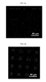
- FIGS. 4a and 4b are optical microscopic photographs showing a mesh-type source electrode prepared according to the processes depicted in FIG. 3 .
- the arrangements, the shapes, and the sizes of the electrode regions together with the apertures in the mesh-type source electrode may be adjusted with varying the patterns of the photomask. Since the organic light-emitting layer emits light through the apertures, hereinafter, an electrode region of the mesh-type source electrode will be referred to the region covered with the electrode, and the aperture region will be referred to a light emission region.
- FIG. 4a shows a fabricated mesh-type source electrode in which the electrode region has a width of about 20 ⁇ m and the light emission region has a width of about 40 ⁇ m.
- the electrode region has a width of about 5 ⁇ m and the light emission region has a width of about 20 ⁇ m.
- the charge transport and flow in the semiconductor layer may be controlled by adjusting the relative size of the electrode region to the light emission region so that the light emission characteristics of the organic light-emitting layer are optimized.
- FIGS. 5a to 5c are photographs showing quasi-surface emission at the organic light-emitting transistor depending on the voltage between the gate electrode and the source electrode.
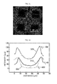
- FIG. 5d is a graph showing the spatial distribution of brightness in FIGS. 5a to 5c .
- FIGS. 5a to 5c show quasi-surface emission of the organic light-emitting transistor when the voltages applied between the gate electrode and the source electrode are 0 V, -40 V, and +40 V, respectively.
- a mesh-type source electrode in which each aperture has a width of about 40 ⁇ m and a gap between two neighboring apertures (i.e., a line width of the electrode region) is about 20 ⁇ m.
- a semiconductor layer of pentacene, having the p-type semiconducting properties is used.
- Three graphs 510, 520, 530 depicted in FIG. 5d represent the spatial distributions of brightness in a region (depicted with a line) across a single aperture in FIGS. 5a to 5c , respectively.
- the charges are partially transported so that light is emitted only in the small region along the perimeter of each aperture.
- FIG. 5b when the voltage between the gate electrode and the source electrode is -40 V, a channel is formed and the charge transport occurs in the semiconductor layer. In addition to the charge transport in the plane of the semiconductor layer, the out-of-plane charge transport through the apertures is promoted by the voltage difference between the source electrode and the drain electrode. This results in the recombination of the mobile charges with the charges having the opposite polarity in the organic light-emitting layer. Note that for the case of the aperture having a width of about 40 ⁇ m, the in-plane charge transport is still limited and light emission over the entire aperture is not obtained.
- FIGS. 6a to 6c are photographs showing quasi-surface emission in the organic light-emitting transistor depending on the voltage between a source electrode and a drain electrode.
- FIG. 6d is a graph showing the spatial distribution of brightness in FIG. 6c .
- FIGS. 6a to 6c show quasi-surface emission of the organic light-emitting transistor when the voltages applied between the drain electrode and the source electrode are 0 V, -5 V and -8.5 V, respectively.
- a mesh-type source electrode in which each aperture has a width of about 20 ⁇ m and a gap between two neighboring apertures (i.e., a line width of the electrode region) is about 20 ⁇ m.
- a semiconductor layer of pentacene, having the p-type semiconducting properties is used.
- the graph depicted in FIG. 6d shows the spatial distribution of brightness in a region (depicted with a line) across a single aperture in FIG. 6c .
- the width of the aperture in the mesh-type source electrode is reduced from about 40 ⁇ m to about 20 ⁇ m as shown in FIG. 5 and FIG. 6 , respectively, the charge transport occurs through nearly the entire aperture. In this case, quasi-surface light emission covering nearly the entire aperture is produced. From the spatial distribution of brightness depicted in FIG. 6d , the distance of the in-plane charge transport is estimated to be about 10 ⁇ m.
- the organic light-emitting transistor according to the embodiments described above shows quasi-surface emission characteristics acquired by the employment of a mesh-type source electrode.
- the organic light-emitting transistor adopting a mesh-type source electrode may produce a surface emission level similar to that of the organic light-emitting diode.
- an aperture ratio, brightness, and light emission efficiency of the organic light-emitting transistor may be superior to those of an organic light-emitting diode.
- Another advantage is that the production cost may be reduced since an additional driving element such as a thin-film-transistor is not needed.
- the manufacturing methods according to the aspect of the present disclosure can be easily realized by conventional lithographic or ink-jet printing processes of fabricating the electrode and the semiconductor, and may be applicable for new organic optoelectronic devices and flexible displays.
Landscapes
- Physics & Mathematics (AREA)
- Optics & Photonics (AREA)
- Engineering & Computer Science (AREA)
- Manufacturing & Machinery (AREA)
- Chemical & Material Sciences (AREA)
- Materials Engineering (AREA)
- Nanotechnology (AREA)
- Electroluminescent Light Sources (AREA)
- Thin Film Transistor (AREA)
Abstract
Description
- Embodiments relate to a quasi-surface emission vertical-type organic light-emitting transistor and a method of manufacturing the same.
- An organic light-emitting transistor enables to control light-emitting characteristics without an additional driving element whereas an organic light-emitting diode always needs a driving element such as a thin-film-transistor. As a result, the organic light-emitting transistor has a high aperture ratio and high light emission efficiency, and thus it is promising as a next-generation light-emitting device.
- Although the organic light-emitting transistor has such intrinsic merits, line-type emission characteristics are necessarily achieved in organic light-emitting transistors where a source electrode and a drain electrode are laterally located on the same plane. In other words, effective light emission is occupied only in a small region out of the entire device. In order to overcome this problem, an organic light-emitting transistor having an interdigitated electrode or a trilayer organic light-emitting transistor has been proposed. However, the increase of the light emission area by the device configuration in a simple additive manner is still limited and is not sufficient for practical applications of the organic light-emitting transistor.
- As an alternative to the simple addition of the light emission area, a metal-insulator-semiconductor structure, which can be applied in a vertical-type organic light-emitting device, has been proposed. Recently, a low-voltage and low-power organic light-emitting transistor using carbon nano-tubes as a source electrode has been also proposed. Because of the random distribution and no alignment of the carbon nano-tubes in a layer used as the source electrode, the resultant surface roughness lowers the stability and the lifetime of the device. In addition, the light emission efficiency and the reproducibility are possibly deteriorated due to the poor connectivity and the spatial non-uniformity inherent to an assembled structure of carbon nano-tubes.
- The present disclosure is directed to providing a new organic light-emitting transistor having a large light emission area, and a cost-effective technique for combining a light-emitting element and a driving transistor. This organic light-emitting transistor can be used for next-generation displays and various optoelectronic devices beyond the organic light-emitting diode.
- An organic light-emitting transistor according to an embodiment may include a mesh-type source electrode having a plurality of apertures in an array pattern. The mesh-type source electrode may be located between the gate electrode and the drain electrode.
- The organic light-emitting transistor may further include the gate electrode and the drain electrode. The organic light-emitting transistor may further include an insulator located between the gate electrode and the mesh-type source electrode. The organic light-emitting transistor may further include a semiconductor layer and an organic light-emitting layer located between the mesh-type source electrode and the drain electrode. The organic light-emitting transistor may further include a source insulator located between the mesh-type source electrode and the semiconductor layer.
- In the organic light-emitting transistor, the drain electrode and/or the gate electrode may include a plurality of apertures in an array pattern.
- In the organic light-emitting transistor, each of the plurality of apertures may have a circular, oval, or polygonal shape. Each of the plurality of apertures may have a width of 200 µm or below, and a gap between two neighboring apertures in the plurality of apertures may be 200 µm or below.
- In the organic light-emitting transistor, the plurality of apertures may be formed as a plurality of holes or a plurality of strips. For example, the plurality of apertures may be formed through the mesh-type source electrode and may be formed as a plurality of holes in a two-dimensional array. Alternatively, the plurality of apertures may extend from one side of the mesh-type source electrode to the other side of the mesh-type electrode and may be formed as a plurality of strips in one-dimensional array.
- A method of manufacturing an organic light-emitting transistor according to an embodiment may include: forming an electrode layer; and patterning the electrode layer to construct a mesh-type source electrode having a plurality of apertures in an array pattern. Before forming the electrode layer, the method of manufacturing an organic light-emitting transistor may further include: forming a gate electrode; and forming a gate insulator film on the gate electrode. In addition, the method of manufacturing an organic light-emitting transistor may further include: forming a semiconductor layer on the mesh-type source electrode; forming an organic light-emitting layer on the semiconductor layer; and forming a drain electrode on the organic light-emitting layer.
- In the method of manufacturing an organic light-emitting transistor, said patterning of the electrode layer may include: forming a source insulator on the electrode layer, wherein the source insulator is made of a photoresist; irradiating ultraviolet rays to a predetermined area of the source insulator made of photoresist; removing the region irradiated by ultraviolet rays from the source insulator made of photoresist; and etching the electrode layer by using the source insulator as an etching mask.
- In the method of manufacturing an organic light-emitting transistor, each of the plurality of apertures may have a circular, oval, or polygonal shape. Each of the plurality of apertures may have a width of 200 µm or below, and a gap between two neighboring apertures in the plurality of apertures may be 200 µm or below.
- In the method of manufacturing an organic light-emitting transistor, the plurality of apertures is formed as a plurality of holes or a plurality of strips. For example, the plurality of apertures may be formed through the mesh-type source electrode and may be formed as a plurality of holes in a two-dimensional array. Alternatively, the plurality of apertures may extend from one side of the mesh-type source electrode to the other side of the mesh-type electrode and may be formed as a plurality of strips in one-dimensional array.
- The organic light-emitting transistor according to an aspect of the present disclosure shows quasi-surface emission characteristics acquired by the employment of a mesh-type source electrode. The organic light-emitting transistor with a mesh-type source electrode may produce a surface emission level similar to that of the organic light-emitting diode. Moreover, an aperture ratio, brightness, and light emission efficiency of the organic light-emitting transistor may be superior to those of an organic light-emitting diode. Another advantage is that the production cost may be reduced since an additional driving element such as a thin-film-transistor is not needed.
- The manufacturing methods according to an aspect of the present disclosure can be easily realized by conventional lithographic or ink-jet printing processes of fabricating the electrode and the semiconductor, and may be applicable for new organic optoelectronic devices and flexible displays.
- The above and other aspects, features and advantages of the disclosed exemplary embodiments will be more apparent from the following detailed description taken in conjunction with the accompanying drawings in which:
-
FIG. 1a is a cross-sectional view showing a quasi-surface emission vertical-type organic light-emitting transistor according to an embodiment; -
FIG. 1b is a plane view showing a mesh-type source electrode of the organic light-emitting transistor depicted inFIG. 1a ; -
FIGS. 2a and 2b are diagrams showing injection and flow of charges toward an aperture from the boundary of a source electrode of the organic light-emitting transistor according to embodiments; -
FIGS. 3a to 3e are cross-sectional views illustrating a fabrication process of a mesh-type source electrode for manufacturing an organic light-emitting transistor according to an embodiment; -
FIGS. 4a and 4b are optical microscopic photographs showing a mesh-type source electrode fabricated according to embodiments; -
FIGS. 5a to 5c are optical microscopic photographs showing quasi-surface emission in the organic light-emitting transistor by applying a voltage between a gate electrode and a source electrode; -
FIG. 5d is a graph showing the spatial distribution of brightness inFIGS. 5a to 5c ; -
FIGS. 6a to 6c are optical microscopic photographs showing quasi-surface emission in the organic light-emitting transistor by applying a voltage between a source electrode and a drain electrode; and -
FIG. 6d is a graph showing the spatial distribution of brightness inFIG. 6c . - Hereinafter, embodiments of the present disclosure will be described in detail with reference to the accompanying drawings.
-
FIG. 1a is a cross-sectional view showing an organic light-emitting transistor according to an embodiment, andFIG. 1b is a plane view showing a mesh-type source electrode of the organic light-emitting transistor depicted inFIG. 1a . The organic light-emitting transistor according to embodiments may be a vertical-type organic light-emitting transistor where the light emission is generated by vertical movement of charges and has quasi-surface emission characteristics due to a large light emission area. - Referring to
FIGS. 1a and 1b , the organic light-emitting transistor according to an embodiment may include a mesh-type source electrode 40. The mesh-type source electrode 40 may have a plurality ofapertures 400 arranged in an array pattern. Eachaperture 400 may be formed through thesource electrode 40. In an embodiment, the shape of eachaperture 400 may be a hole formed within thesource electrode 40 when thesource electrode 40 is viewed from the above. In another embodiment, the shape of eachaperture 400 may be a strip extending from the one side of thesource electrode 40 to the other side of thesource electrode 40 when thesource electrode 40 is viewed from the above. The hole or strip forming theaperture 400 may have a cross-sectional shape such as a circle, an oval or a polygon. - Furthermore, the organic light-emitting transistor may include at least one of a
substrate 10, agate electrode 20, and agate insulator 30 below the mesh-type source electrode 40. Above the mesh-type source electrode 40, at least one ofsource insulator 50, asemiconductor layer 60, an organiclight emitting layer 70, and adrain electrode 80 may be included. In an embodiment, thesource insulator 50 is made of a photoresist (PR). The mesh-type source electrode 40 may be located between thedrain electrode 80 in the top and thegate electrode 20 in the bottom. - The
substrate 10 supports the entire structure of the organic light-emitting transistor. Thesubstrate 10 may be made of glass, quartz, polymer resin (for example, plastic or the like), silicon, or other suitable materials. - The
gate electrode 20 may be formed on thesubstrate 10. Thegate electrode 20 may be made of an electrically-conductive transparent material (for example, indium-tin-oxide), a metal such as aluminum (Al), gold (Au), silver (Ag) or the like, a conductive organic material, a nonmetallic material such as a conductive polymer or an assembly of conductive particles, or other suitable conductive material. Thegate electrode 20 may be formed by vacuum deposition, without being limited thereto. - The
gate insulator 30 may be formed on thegate electrode 20. Thegate insulator 30 may be made of an electrically-insulating inorganic material such as silicon oxide (SiO2), an organic material such as an insulating polymer, or other suitable material having properties to block the electric current and to apply an electric field at thegate electrode 20 to thesemiconductor layer 60 for the charge transport. - The mesh-
type source electrode 40 may be formed on thegate insulator 30. The source electrode 40 may be made of a material which has excellent electric conductivity, facilitates the charge injection to thesemiconductor layer 60, and is capable of being patterned. For example, thesource electrode 40 may be made of a metal such as gold (Au), a nonmetallic material such as a conductive organic material or an assembly of conductive particles, or other suitable conductive material. The source electrode 40 may be formed by vacuum-deposition and patterned by photolithography, without being limited thereto. - In an embodiment, the
source insulator 50, made of the photoresist, on thesource electrode 40 may be served to pattern thesource electrode 40. If no insulator is present on thesource electrode 40, charges are injected and transported by the voltage difference between thesource electrode 40 and thedrain electrode 80 irrespective of the gate voltage. This causes light emission similar to the organic light-emitting diode, meaning that the switching function of the driving transistor disappears. - The
semiconductor layer 60 may be formed on thegate insulator 30 in theapertures 400 and on thesource insulator 50. Thesemiconductor layer 60 may be made of a low-molecular organic semiconductor or a polymeric semiconductor material, an inorganic semiconductor material, or other suitable material capable of forming a charge transporting channel under a voltage. In addition, thesemiconductor layer 60 may be made of a material containing metal particles to the above material. In an embodiment, thesemiconductor layer 60 may be made of pentacene having the p-type semiconducting properties, without being limited thereto. - The organic light-emitting
layer 70 may be formed on thesemiconductor layer 60. The organic light-emittinglayer 70 may be configured into a single layer structure composed of a p-type semiconductor together with an n-type semiconductor, an ambipolar semiconductor material, or the like. A bilayer or trilayer structure can be also used for improving light emission efficiency or controlling light color. In an embodiment, the organic light-emittinglayer 70 may be configured with a bilayer of α-NPD (N,N'-di(1-naphthyl)-N,N'-diphenylbenzidine) and Alq3 ((tri-(8-hydroxyquinoline)aluminum) prepared by vacuum deposition, without being limited thereto. - The
drain electrode 80 may be formed on the organic light-emittinglayer 70. Thedrain electrode 80 may be made of a metallic or nonmetallic material, which has excellent electric conductivity and facilitates the charge injection to thesemiconductor layer 60, similar to thesource electrode 40. In an embodiment, thedrain electrode 80 may be configured as a bilayer of lithium fluoride (LiF) and aluminum (Al), without being limited thereto. - In the organic light-emitting transistor as described above according to this embodiment, the
source electrode 40 is formed in a mesh type with the plurality ofapertures 400 which leads directly to the enhancement of the charge injection and transport through thesemiconductor layer 60 toward the organic light-emittinglayer 70. As a result, the effective emission of the organic light-emittinglayer 70 exhibits quasi-surface emission characteristics that can vary with a gate voltage. - Specifically, charges are injected into the
semiconductor layer 60 through theaperture 400 of thesource electrode 40, and mobile charges are recombined with charges having the opposite polarity present in the organic light-emittinglayer 70. Charge injection to thesemiconductor layer 60, charge recombination in the organic light-emittinglayer 70, and the resultant light emission area and brightness are primarily influenced by the physical dimension of theaperture 400. The light emission characteristics of the organic light-emitting transistor can be optimized by adjusting the shape and the size of eachaperture 400 in addition to the gap between the neighboringapertures 400 in the mesh-type source electrode 40. - In an embodiment, the mesh-
type source electrode 40 may include the plurality ofsquare apertures 400. Here, eachaperture 400 may have a width (W) of several nanometers to about 200 µm in each side. In addition, a gap between the neighboring apertures 400 (i.e., a line width of the source electrode 40) may be several nanometers to about 200 µm. This is just one of the examples. It should be emphasized that the shape and the size of eachaperture 400 and the structural arrangement of theapertures 400 in thesource electrode 40 are not limited to the above. - In a conventional vertical-type organic light-emitting transistor, the gate electrode is located between a source electrode and a drain electrode, and a charge flow between the source and the drain is adjusted by a gate voltage. In this case, the leakage current at the gate electrode is considerably large. In contrast, in the vertical-type organic light-emitting transistor of this embodiment, the
source electrode 40 is located between thedrain electrode 80 and thegate electrode 20, which may reduce the leakage current. The key feature of the mesh-type source electrode 40 is that an electric field generated from thegate electrode 20 should penetrate through theapertures 400 of thesource electrode 40 to effectively control the charge injection and transport by a gate voltage between thesource electrode 40 and thedrain electrode 80. - In another embodiment, the organic light-emitting transistor may also be configured such that the gate electrode and/or the drain electrode have the plurality of the apertures. For example, the plurality of holes arranged two-dimensionally or the plurality of strip-type apertures arranged one-dimensionally may be formed in the gate electrode and/or the drain electrode. Besides the mesh-type source electrode, the spatial distribution of the electric field lines can be varied with the geometrical parameters of the gate and/or drain electrodes with the apertures for the optimization of the charge injection and transport, the charge recombination, and the resultant light emission in the organic light-emitting transistor.
-
FIGS. 2a and 2b are diagrams showing injection and flow of charges in each aperture of a source electrode of the organic light-emitting transistor according to embodiments. Arrows depicted inFIGS. 2a and 2b represent a charge flow direction in theapertures source electrodes - Referring to
FIG. 2a , in an embodiment, thesource electrode 40 includes the plurality ofapertures 400 in a closed configuration. Theapertures 400 may be formed as the plurality of holes in a two-dimensional array within thesource electrode 40. In thesource electrode 40 depicted inFIG. 2a , the charge injection and flow occur in a two-dimensional manner due to the closed boundary of theaperture 400, and consequently, the recombination zone of the charges in the organic light-emittinglayer 70 is expanded to cover theaperture 400. This results in quasi-surface emission, high light emission efficiency, and high brightness. - Referring to
FIG. 2b , in another embodiment, thesource electrode 41 includes the plurality ofapertures 410 in an opened configuration. Theapertures 410 may be formed as a plurality of strips extending from the one side of thesource electrode 41 to the other side of thesource electrode 41 when thesource electrode 41 is viewed from the above. The plurality of strips may be formed in a one-dimensional array pattern. In this case, an electrode portion of thesource electrode 41 has a structure similar to comb teeth. In thesource electrode 41 shown inFIG. 2b , the charge injection and flow occur in a one-dimensional manner due to the open configuration of theapertures 410, which causes relatively small light emission area and low efficiency compared to the mesh-type structure depicted inFIG. 2a . - However, the shapes of the
source electrodes apertures FIGS. 2a and 2b are just examples, and the shape, the arrangement and size of apertures formed in an electrode of the organic light-emitting transistor are not limited toFIGS. 2a and 2b . For instance, each aperture may have a cross-sectional shape of a circle, an oval, or a polygon. In addition, the term "mesh-type electrode" used in the present disclosure is intended to include all cases in which the apertures formed in the electrode have a two-dimensionally closed or a one-dimensionally open configuration, and is not intended to limit the apertures to specific locations, shapes or arrangements. -
FIGS. 3a to 3e are cross-sectional views for illustrating a process of fabricating a mesh-type source electrode in manufacturing an organic light-emitting transistor according to an embodiment. - Referring to
FIG. 3a , first, agate insulator 30 may be prepared. A gate electrode (not shown) may be formed on a substrate (not shown) made of glass or plastic, and agate insulator 30 may be formed on the gate electrode. Next, asource electrode 40 may be formed on thegate insulator 30. Here, thesource electrode 40 may be a single film formed on theentire gate insulator 30. For example, a layer of gold (Au) may be formed on the entire surface of thegate insulator 30 by vacuum deposition as thesource electrode 40, without being limited thereto. - Referring to
FIG. 3b , asource insulator 50 may be formed on thesource electrode 40. Thesource insulator 50, made of the photoresist in this embodiment, may be served to pattern thesource electrode 40 having apertures. Thesource insulator 50 may be prepared by spin-coating, without being limited thereto. - Referring to
FIG. 3c , aphotomask 55 may be located on thesource insulator 50 made of the photoresist, and ultraviolet rays (UV) may be irradiated above thephotomask 55. Thephotomask 55 may be prepared to have a pattern corresponding to the shape of the plurality of apertures which is to be formed in thesource electrode 40. After irradiating ultraviolet rays, thephotomask 55 may be removed. - Referring to
FIG. 3d , the region of thesource insulator 50 made of the photoresist onto which ultraviolet rays are irradiated may be removed using a photoresist developer. Accordingly, patterns corresponding to thephotomask 55 are formed in thesource insulator 50, and the portion of thesource electrode 40 in the regions where the photoresist was developed may not be covered with thesource insulator 50. - Referring to
FIG. 3e , a mesh-type source electrode 40 having the plurality ofapertures 400 may be formed by using thesource insulator 50 as an etching mask. For example, thesource electrode 40 may be etched by plasma etching, without being limited thereto. Then, a semiconductor layer (not shown), an organic light-emitting layer (not shown), and a drain electrode (not shown) may be sequentially formed on thegate insulator 30 through theapertures 400 and on thesource insulator 50. In the organic light-emitting transistor manufactured according to the method of this embodiment, since thesource electrode 40 is formed prior to the process of forming a semiconductor layer and an organic light-emitting layer, the damage of an organic material layer by a solution process or an etching process is basically avoided. -
FIGS. 4a and 4b are optical microscopic photographs showing a mesh-type source electrode prepared according to the processes depicted inFIG. 3 . The arrangements, the shapes, and the sizes of the electrode regions together with the apertures in the mesh-type source electrode may be adjusted with varying the patterns of the photomask. Since the organic light-emitting layer emits light through the apertures, hereinafter, an electrode region of the mesh-type source electrode will be referred to the region covered with the electrode, and the aperture region will be referred to a light emission region.FIG. 4a shows a fabricated mesh-type source electrode in which the electrode region has a width of about 20 µm and the light emission region has a width of about 40 µm.FIG. 4b shows a mesh-type source electrode in which the electrode region has a width of about 5 µm and the light emission region has a width of about 20 µm. The charge transport and flow in the semiconductor layer may be controlled by adjusting the relative size of the electrode region to the light emission region so that the light emission characteristics of the organic light-emitting layer are optimized. -
FIGS. 5a to 5c are photographs showing quasi-surface emission at the organic light-emitting transistor depending on the voltage between the gate electrode and the source electrode.FIG. 5d is a graph showing the spatial distribution of brightness inFIGS. 5a to 5c . -
FIGS. 5a to 5c show quasi-surface emission of the organic light-emitting transistor when the voltages applied between the gate electrode and the source electrode are 0 V, -40 V, and +40 V, respectively. Here, a mesh-type source electrode in which each aperture has a width of about 40 µm and a gap between two neighboring apertures (i.e., a line width of the electrode region) is about 20 µm. In this embodiment, a semiconductor layer of pentacene, having the p-type semiconducting properties, is used. Threegraphs FIG. 5d represent the spatial distributions of brightness in a region (depicted with a line) across a single aperture inFIGS. 5a to 5c , respectively. - Referring to
FIG. 5c , when the voltage between the gate electrode and the source electrode is +40 V, the charges in the semiconductor layer are not accumulated in the channel region and essentially no charge transport occurs. Thus, no light emission is produced. - Referring to
FIG. 5a , when the voltage between the gate electrode and the source electrode is 0 V, the charges are partially transported so that light is emitted only in the small region along the perimeter of each aperture. Referring toFIG. 5b , when the voltage between the gate electrode and the source electrode is -40 V, a channel is formed and the charge transport occurs in the semiconductor layer. In addition to the charge transport in the plane of the semiconductor layer, the out-of-plane charge transport through the apertures is promoted by the voltage difference between the source electrode and the drain electrode. This results in the recombination of the mobile charges with the charges having the opposite polarity in the organic light-emitting layer. Note that for the case of the aperture having a width of about 40 µm, the in-plane charge transport is still limited and light emission over the entire aperture is not obtained. -
FIGS. 6a to 6c are photographs showing quasi-surface emission in the organic light-emitting transistor depending on the voltage between a source electrode and a drain electrode.FIG. 6d is a graph showing the spatial distribution of brightness inFIG. 6c . -
FIGS. 6a to 6c show quasi-surface emission of the organic light-emitting transistor when the voltages applied between the drain electrode and the source electrode are 0 V, -5 V and -8.5 V, respectively. Here, a mesh-type source electrode in which each aperture has a width of about 20 µm and a gap between two neighboring apertures (i.e., a line width of the electrode region) is about 20 µm. In this embodiment, a semiconductor layer of pentacene, having the p-type semiconducting properties, is used. The graph depicted inFIG. 6d shows the spatial distribution of brightness in a region (depicted with a line) across a single aperture inFIG. 6c . - When the width of the aperture in the mesh-type source electrode is reduced from about 40 µm to about 20 µm as shown in
FIG. 5 andFIG. 6 , respectively, the charge transport occurs through nearly the entire aperture. In this case, quasi-surface light emission covering nearly the entire aperture is produced. From the spatial distribution of brightness depicted inFIG. 6d , the distance of the in-plane charge transport is estimated to be about 10 µm. - The organic light-emitting transistor according to the embodiments described above shows quasi-surface emission characteristics acquired by the employment of a mesh-type source electrode. The organic light-emitting transistor adopting a mesh-type source electrode may produce a surface emission level similar to that of the organic light-emitting diode. Moreover, an aperture ratio, brightness, and light emission efficiency of the organic light-emitting transistor may be superior to those of an organic light-emitting diode. Another advantage is that the production cost may be reduced since an additional driving element such as a thin-film-transistor is not needed.
- The manufacturing methods according to the aspect of the present disclosure can be easily realized by conventional lithographic or ink-jet printing processes of fabricating the electrode and the semiconductor, and may be applicable for new organic optoelectronic devices and flexible displays.
- While the present disclosure has been described with reference to embodiments depicted in the drawings, they are just examples, and it will be understood by those skilled in the art that various changes and modifications may be made thereto. However, such changes and modification should be interpreted as being included in the scope of the present disclosure. Therefore, the sincere scope of the present disclosure should be defined by the appended claims.
Claims (15)
- An organic light-emitting transistor comprising a mesh-type source electrode having a plurality of apertures in an array pattern.
- The organic light-emitting transistor according to claim 1, further comprising a gate electrode and a drain electrode,
wherein the mesh-type source electrode is located between the gate electrode and the drain electrode. - The organic light-emitting transistor according to claim 2, further comprising an insulator located between the gate electrode and the mesh-type source electrode.
- The organic light-emitting transistor according to claim 2, further comprising a semiconductor layer and an organic light-emitting layer located between the mesh-type source electrode and the drain electrode.
- The organic light-emitting transistor according to claim 4, further comprising a source insulator located between the mesh-type source electrode and the semiconductor layer.
- The organic light-emitting transistor according to claim 2, wherein the drain electrode comprises a plurality of apertures in an array pattern.
- The organic light-emitting transistor according to claim 2, wherein the gate electrode comprises a plurality of apertures in an array pattern.
- The organic light-emitting transistor according to claim 1, wherein each of the plurality of apertures has a width of 200 µm or below, and wherein a gap between two neighboring apertures in the plurality of apertures is 200 µm or below.
- The organic light-emitting transistor according to claim 1, wherein the plurality of apertures is formed as a plurality of holes or a plurality of strips.
- A method of manufacturing an organic light-emitting transistor, the method comprising:forming an electrode layer; andpatterning the electrode layer to form a mesh-type source electrode having a plurality of apertures in an array pattern.
- The method of manufacturing an organic light-emitting transistor according to claim 10, before said forming of an electrode layer, further comprising:forming a gate electrode; andforming a gate insulator on the gate electrode,wherein the mesh-type source electrode is located on the gate insulator.
- The method of manufacturing an organic light-emitting transistor according to claim 10, further comprising:forming a semiconductor layer on the mesh-type source electrode;forming an organic light-emitting layer on the semiconductor layer; andforming a drain electrode on the organic light-emitting layer.
- The method of manufacturing an organic light-emitting transistor according to claim 10, wherein said patterning of the electrode layer comprises:forming a source insulator on the electrode layer, wherein the source insulator is made of a photoresist;irradiating ultraviolet rays to a predetermined area of the source insulator made of photoresist;removing the region irradiated by ultraviolet rays from the source insulator made of photoresist; andetching the electrode layer by using the source insulator as an etching mask.
- The method of manufacturing an organic light-emitting transistor according to claim 10, wherein each of the plurality of apertures has a width of 200 µm or below, and wherein a gap between two neighboring apertures in the plurality of apertures is 200 µm or below.
- The method of manufacturing an organic light-emitting transistor according to claim 10, wherein the plurality of apertures is formed as a plurality of holes or a plurality of strips.
Applications Claiming Priority (1)
| Application Number | Priority Date | Filing Date | Title |
|---|---|---|---|
| KR1020130007683A KR101427776B1 (en) | 2013-01-23 | 2013-01-23 | Quasi-surface emission vertical-type organic light-emitting transistors and method for manufacturing the same |
Publications (2)
| Publication Number | Publication Date |
|---|---|
| EP2760060A1 true EP2760060A1 (en) | 2014-07-30 |
| EP2760060B1 EP2760060B1 (en) | 2021-04-21 |
Family
ID=49766999
Family Applications (1)
| Application Number | Title | Priority Date | Filing Date |
|---|---|---|---|
| EP13197627.6A Active EP2760060B1 (en) | 2013-01-23 | 2013-12-17 | Quasi-surface emission vertical-type organic light-emitting transistors and method of manufacturing the same |
Country Status (4)
| Country | Link |
|---|---|
| US (1) | US20140203249A1 (en) |
| EP (1) | EP2760060B1 (en) |
| JP (1) | JP2014143179A (en) |
| KR (1) | KR101427776B1 (en) |
Cited By (1)
| Publication number | Priority date | Publication date | Assignee | Title |
|---|---|---|---|---|
| CN107004694A (en) * | 2014-11-28 | 2017-08-01 | 乐金显示有限公司 | Flexible display apparatus |
Families Citing this family (5)
| Publication number | Priority date | Publication date | Assignee | Title |
|---|---|---|---|---|
| CN104992961B (en) * | 2015-07-21 | 2018-03-30 | 京东方科技集团股份有限公司 | Organic electroluminescent transistor (TFT) array substrate and preparation method thereof, display device |
| KR101730902B1 (en) | 2015-10-19 | 2017-04-27 | 서울대학교산학협력단 | Vertical-type organic light-emitting transistors with reduced leakage current and method for fabricating the same |
| CN105489761A (en) * | 2016-01-14 | 2016-04-13 | 中国计量学院 | Vertical organic field effect transistor based on screen electrode |
| WO2019109310A1 (en) * | 2017-12-07 | 2019-06-13 | 深圳市柔宇科技有限公司 | Thin film transistor and manufacturing method thereof, array substrate, and display device |
| KR102791452B1 (en) * | 2019-04-26 | 2025-04-08 | 제이에스알 가부시키가이샤 | Method for compensating the brightness of a display and display |
Citations (4)
| Publication number | Priority date | Publication date | Assignee | Title |
|---|---|---|---|---|
| WO2007080575A1 (en) * | 2006-01-09 | 2007-07-19 | Technion Research And Development Foundation Ltd. | Transistor structures and methods of fabrication thereof |
| US20090179195A1 (en) * | 2005-12-02 | 2009-07-16 | Dai Nippon Printing Co., Ltd. | Organic Luminescence Transistor Device and Manufacturing Method Thereof |
| US20100090203A1 (en) * | 2007-01-09 | 2010-04-15 | Dai Nippon Printing Co., Ltd. | Organic Light-Emitting Element, Organic Light-Emitting Transistor, and Light-Emitting Display Device |
| US20100155705A1 (en) * | 2008-12-24 | 2010-06-24 | Jung-Han Shin | Display Device Including Organic Light-Emitting Transistor And Method Of Fabricating The Display Device |
Family Cites Families (9)
| Publication number | Priority date | Publication date | Assignee | Title |
|---|---|---|---|---|
| JP3403136B2 (en) * | 1999-12-28 | 2003-05-06 | 株式会社東芝 | Method for manufacturing switching element, switching element and switching element array |
| JP4100351B2 (en) * | 2004-02-09 | 2008-06-11 | セイコーエプソン株式会社 | Thin film transistor manufacturing method |
| GB0517195D0 (en) * | 2005-08-23 | 2005-09-28 | Cambridge Display Tech Ltd | Molecular electronic device structures and fabrication methods |
| JP2007109564A (en) * | 2005-10-14 | 2007-04-26 | Pioneer Electronic Corp | Light emitting element and display device |
| JP4808479B2 (en) * | 2005-11-28 | 2011-11-02 | 大日本印刷株式会社 | ORGANIC LIGHT EMITTING TRANSISTOR ELEMENT, ITS MANUFACTURING METHOD, AND LIGHT EMITTING DISPLAY DEVICE |
| JP4934774B2 (en) * | 2006-09-05 | 2012-05-16 | 大日本印刷株式会社 | Organic light emitting transistor and display device |
| JP4962500B2 (en) * | 2006-12-28 | 2012-06-27 | 大日本印刷株式会社 | Organic transistor element, manufacturing method thereof, organic light emitting transistor and light emitting display device |
| JP2009070708A (en) * | 2007-09-13 | 2009-04-02 | Casio Comput Co Ltd | Display device and manufacturing method of display device |
| EP2458937A4 (en) * | 2009-07-21 | 2013-10-30 | Showa Denko Kk | LIGHT EMITTING DEVICE, METHOD FOR MANUFACTURING LIGHT EMITTING ELEMENT, IMAGE DISPLAY DEVICE, AND LIGHTING DEVICE |
-
2013
- 2013-01-23 KR KR1020130007683A patent/KR101427776B1/en active Active
- 2013-10-23 US US14/060,871 patent/US20140203249A1/en not_active Abandoned
- 2013-11-27 JP JP2013244989A patent/JP2014143179A/en active Pending
- 2013-12-17 EP EP13197627.6A patent/EP2760060B1/en active Active
Patent Citations (4)
| Publication number | Priority date | Publication date | Assignee | Title |
|---|---|---|---|---|
| US20090179195A1 (en) * | 2005-12-02 | 2009-07-16 | Dai Nippon Printing Co., Ltd. | Organic Luminescence Transistor Device and Manufacturing Method Thereof |
| WO2007080575A1 (en) * | 2006-01-09 | 2007-07-19 | Technion Research And Development Foundation Ltd. | Transistor structures and methods of fabrication thereof |
| US20100090203A1 (en) * | 2007-01-09 | 2010-04-15 | Dai Nippon Printing Co., Ltd. | Organic Light-Emitting Element, Organic Light-Emitting Transistor, and Light-Emitting Display Device |
| US20100155705A1 (en) * | 2008-12-24 | 2010-06-24 | Jung-Han Shin | Display Device Including Organic Light-Emitting Transistor And Method Of Fabricating The Display Device |
Cited By (2)
| Publication number | Priority date | Publication date | Assignee | Title |
|---|---|---|---|---|
| CN107004694A (en) * | 2014-11-28 | 2017-08-01 | 乐金显示有限公司 | Flexible display apparatus |
| CN107004694B (en) * | 2014-11-28 | 2021-09-17 | 乐金显示有限公司 | Flexible display device |
Also Published As
| Publication number | Publication date |
|---|---|
| JP2014143179A (en) | 2014-08-07 |
| US20140203249A1 (en) | 2014-07-24 |
| KR101427776B1 (en) | 2014-08-12 |
| KR20140094970A (en) | 2014-07-31 |
| EP2760060B1 (en) | 2021-04-21 |
Similar Documents
| Publication | Publication Date | Title |
|---|---|---|
| TWI851388B (en) | Display panel | |
| EP2760060B1 (en) | Quasi-surface emission vertical-type organic light-emitting transistors and method of manufacturing the same | |
| KR101885451B1 (en) | Array substrate, display device having the same, and manufacturing method thereof | |
| KR102067376B1 (en) | Organic light emitting diode display and method for manufacturing the same | |
| EP2141964B1 (en) | Organic EL element and manufacturing method thereof | |
| CN100485993C (en) | Shadow mask for fabricating organic electroluminescent device | |
| CN108257547B (en) | Electroluminescent display device and method for manufacturing the same | |
| KR102222998B1 (en) | Organic light emitting display device having a channel in pixel defining layer | |
| US20210057648A1 (en) | Organic light-emitting display apparatus and method of manufacturing the same | |
| KR20140099127A (en) | Mask for thin film deposition, the fabrication method thereof, and the fabrication method of the organic light emitting display device using the same | |
| DE112009000595T5 (en) | Electronic components and methods of making the same using solution technology based methods | |
| WO2013118706A1 (en) | Thin-film transistor having three-dimensional structure, and method for manufacturing same | |
| KR20050050495A (en) | Thin film transistors and method of manufacturing thereof | |
| CN101689608B (en) | Organic thin film transistors, organic light emitting devices and organic light emitting displays | |
| KR20160122362A (en) | Mask assembly for thin film deposition | |
| KR20160127221A (en) | Mask frame assembly for thin layer deposition, manufacturing method of the same and manufacturing method of display device there used | |
| US6909108B2 (en) | Structure of quantum dot light emitting diode and method of fabricating the same | |
| CN111554750B (en) | Thin film transistor, preparation method thereof and display panel | |
| CN105401123B (en) | Mask frame assembly and method of making the same | |
| CN1773721A (en) | Organic light emitting display and method of fabricating the same | |
| US20100230668A1 (en) | Organic Light-Emitting Device with Field-Effect Enhanced Mobility | |
| KR101730902B1 (en) | Vertical-type organic light-emitting transistors with reduced leakage current and method for fabricating the same | |
| KR102026763B1 (en) | A method for producing an organic field effect transistor and an organic field effect transistor | |
| HK1197773A (en) | Quasi-surface emission vertical-type organic light-emitting transistors and method of manufacturing the same | |
| HK1197773B (en) | Quasi-surface emission vertical-type organic light-emitting transistors and method of manufacturing the same |
Legal Events
| Date | Code | Title | Description |
|---|---|---|---|
| PUAI | Public reference made under article 153(3) epc to a published international application that has entered the european phase |
Free format text: ORIGINAL CODE: 0009012 |
|
| 17P | Request for examination filed |
Effective date: 20140116 |
|
| AK | Designated contracting states |
Kind code of ref document: A1 Designated state(s): AL AT BE BG CH CY CZ DE DK EE ES FI FR GB GR HR HU IE IS IT LI LT LU LV MC MK MT NL NO PL PT RO RS SE SI SK SM TR |
|
| AX | Request for extension of the european patent |
Extension state: BA ME |
|
| REG | Reference to a national code |
Ref country code: HK Ref legal event code: DE Ref document number: 1197773 Country of ref document: HK |
|
| STAA | Information on the status of an ep patent application or granted ep patent |
Free format text: STATUS: EXAMINATION IS IN PROGRESS |
|
| 17Q | First examination report despatched |
Effective date: 20190716 |
|
| GRAP | Despatch of communication of intention to grant a patent |
Free format text: ORIGINAL CODE: EPIDOSNIGR1 |
|
| STAA | Information on the status of an ep patent application or granted ep patent |
Free format text: STATUS: GRANT OF PATENT IS INTENDED |
|
| INTG | Intention to grant announced |
Effective date: 20201112 |
|
| GRAS | Grant fee paid |
Free format text: ORIGINAL CODE: EPIDOSNIGR3 |
|
| GRAA | (expected) grant |
Free format text: ORIGINAL CODE: 0009210 |
|
| STAA | Information on the status of an ep patent application or granted ep patent |
Free format text: STATUS: THE PATENT HAS BEEN GRANTED |
|
| AK | Designated contracting states |
Kind code of ref document: B1 Designated state(s): AL AT BE BG CH CY CZ DE DK EE ES FI FR GB GR HR HU IE IS IT LI LT LU LV MC MK MT NL NO PL PT RO RS SE SI SK SM TR |
|
| REG | Reference to a national code |
Ref country code: GB Ref legal event code: FG4D |
|
| REG | Reference to a national code |
Ref country code: CH Ref legal event code: EP |
|
| REG | Reference to a national code |
Ref country code: DE Ref legal event code: R096 Ref document number: 602013076996 Country of ref document: DE Ref country code: IE Ref legal event code: FG4D |
|
| REG | Reference to a national code |
Ref country code: AT Ref legal event code: REF Ref document number: 1385570 Country of ref document: AT Kind code of ref document: T Effective date: 20210515 |
|
| REG | Reference to a national code |
Ref country code: LT Ref legal event code: MG9D |
|
| REG | Reference to a national code |
Ref country code: AT Ref legal event code: MK05 Ref document number: 1385570 Country of ref document: AT Kind code of ref document: T Effective date: 20210421 |
|
| REG | Reference to a national code |
Ref country code: NL Ref legal event code: MP Effective date: 20210421 |
|
| PG25 | Lapsed in a contracting state [announced via postgrant information from national office to epo] |
Ref country code: FI Free format text: LAPSE BECAUSE OF FAILURE TO SUBMIT A TRANSLATION OF THE DESCRIPTION OR TO PAY THE FEE WITHIN THE PRESCRIBED TIME-LIMIT Effective date: 20210421 Ref country code: NL Free format text: LAPSE BECAUSE OF FAILURE TO SUBMIT A TRANSLATION OF THE DESCRIPTION OR TO PAY THE FEE WITHIN THE PRESCRIBED TIME-LIMIT Effective date: 20210421 Ref country code: LT Free format text: LAPSE BECAUSE OF FAILURE TO SUBMIT A TRANSLATION OF THE DESCRIPTION OR TO PAY THE FEE WITHIN THE PRESCRIBED TIME-LIMIT Effective date: 20210421 Ref country code: AT Free format text: LAPSE BECAUSE OF FAILURE TO SUBMIT A TRANSLATION OF THE DESCRIPTION OR TO PAY THE FEE WITHIN THE PRESCRIBED TIME-LIMIT Effective date: 20210421 Ref country code: BG Free format text: LAPSE BECAUSE OF FAILURE TO SUBMIT A TRANSLATION OF THE DESCRIPTION OR TO PAY THE FEE WITHIN THE PRESCRIBED TIME-LIMIT Effective date: 20210721 Ref country code: HR Free format text: LAPSE BECAUSE OF FAILURE TO SUBMIT A TRANSLATION OF THE DESCRIPTION OR TO PAY THE FEE WITHIN THE PRESCRIBED TIME-LIMIT Effective date: 20210421 |
|
| PG25 | Lapsed in a contracting state [announced via postgrant information from national office to epo] |
Ref country code: NO Free format text: LAPSE BECAUSE OF FAILURE TO SUBMIT A TRANSLATION OF THE DESCRIPTION OR TO PAY THE FEE WITHIN THE PRESCRIBED TIME-LIMIT Effective date: 20210721 Ref country code: PL Free format text: LAPSE BECAUSE OF FAILURE TO SUBMIT A TRANSLATION OF THE DESCRIPTION OR TO PAY THE FEE WITHIN THE PRESCRIBED TIME-LIMIT Effective date: 20210421 Ref country code: PT Free format text: LAPSE BECAUSE OF FAILURE TO SUBMIT A TRANSLATION OF THE DESCRIPTION OR TO PAY THE FEE WITHIN THE PRESCRIBED TIME-LIMIT Effective date: 20210823 Ref country code: ES Free format text: LAPSE BECAUSE OF FAILURE TO SUBMIT A TRANSLATION OF THE DESCRIPTION OR TO PAY THE FEE WITHIN THE PRESCRIBED TIME-LIMIT Effective date: 20210421 Ref country code: RS Free format text: LAPSE BECAUSE OF FAILURE TO SUBMIT A TRANSLATION OF THE DESCRIPTION OR TO PAY THE FEE WITHIN THE PRESCRIBED TIME-LIMIT Effective date: 20210421 Ref country code: SE Free format text: LAPSE BECAUSE OF FAILURE TO SUBMIT A TRANSLATION OF THE DESCRIPTION OR TO PAY THE FEE WITHIN THE PRESCRIBED TIME-LIMIT Effective date: 20210421 Ref country code: IS Free format text: LAPSE BECAUSE OF FAILURE TO SUBMIT A TRANSLATION OF THE DESCRIPTION OR TO PAY THE FEE WITHIN THE PRESCRIBED TIME-LIMIT Effective date: 20210821 Ref country code: GR Free format text: LAPSE BECAUSE OF FAILURE TO SUBMIT A TRANSLATION OF THE DESCRIPTION OR TO PAY THE FEE WITHIN THE PRESCRIBED TIME-LIMIT Effective date: 20210722 Ref country code: LV Free format text: LAPSE BECAUSE OF FAILURE TO SUBMIT A TRANSLATION OF THE DESCRIPTION OR TO PAY THE FEE WITHIN THE PRESCRIBED TIME-LIMIT Effective date: 20210421 |
|
| REG | Reference to a national code |
Ref country code: DE Ref legal event code: R097 Ref document number: 602013076996 Country of ref document: DE |
|
| PG25 | Lapsed in a contracting state [announced via postgrant information from national office to epo] |
Ref country code: CZ Free format text: LAPSE BECAUSE OF FAILURE TO SUBMIT A TRANSLATION OF THE DESCRIPTION OR TO PAY THE FEE WITHIN THE PRESCRIBED TIME-LIMIT Effective date: 20210421 Ref country code: EE Free format text: LAPSE BECAUSE OF FAILURE TO SUBMIT A TRANSLATION OF THE DESCRIPTION OR TO PAY THE FEE WITHIN THE PRESCRIBED TIME-LIMIT Effective date: 20210421 Ref country code: DK Free format text: LAPSE BECAUSE OF FAILURE TO SUBMIT A TRANSLATION OF THE DESCRIPTION OR TO PAY THE FEE WITHIN THE PRESCRIBED TIME-LIMIT Effective date: 20210421 Ref country code: SK Free format text: LAPSE BECAUSE OF FAILURE TO SUBMIT A TRANSLATION OF THE DESCRIPTION OR TO PAY THE FEE WITHIN THE PRESCRIBED TIME-LIMIT Effective date: 20210421 Ref country code: SM Free format text: LAPSE BECAUSE OF FAILURE TO SUBMIT A TRANSLATION OF THE DESCRIPTION OR TO PAY THE FEE WITHIN THE PRESCRIBED TIME-LIMIT Effective date: 20210421 Ref country code: RO Free format text: LAPSE BECAUSE OF FAILURE TO SUBMIT A TRANSLATION OF THE DESCRIPTION OR TO PAY THE FEE WITHIN THE PRESCRIBED TIME-LIMIT Effective date: 20210421 |
|
| PLBE | No opposition filed within time limit |
Free format text: ORIGINAL CODE: 0009261 |
|
| STAA | Information on the status of an ep patent application or granted ep patent |
Free format text: STATUS: NO OPPOSITION FILED WITHIN TIME LIMIT |
|
| 26N | No opposition filed |
Effective date: 20220124 |
|
| PG25 | Lapsed in a contracting state [announced via postgrant information from national office to epo] |
Ref country code: IS Free format text: LAPSE BECAUSE OF FAILURE TO SUBMIT A TRANSLATION OF THE DESCRIPTION OR TO PAY THE FEE WITHIN THE PRESCRIBED TIME-LIMIT Effective date: 20210821 Ref country code: AL Free format text: LAPSE BECAUSE OF FAILURE TO SUBMIT A TRANSLATION OF THE DESCRIPTION OR TO PAY THE FEE WITHIN THE PRESCRIBED TIME-LIMIT Effective date: 20210421 |
|
| REG | Reference to a national code |
Ref country code: DE Ref legal event code: R119 Ref document number: 602013076996 Country of ref document: DE |
|
| PG25 | Lapsed in a contracting state [announced via postgrant information from national office to epo] |
Ref country code: MC Free format text: LAPSE BECAUSE OF FAILURE TO SUBMIT A TRANSLATION OF THE DESCRIPTION OR TO PAY THE FEE WITHIN THE PRESCRIBED TIME-LIMIT Effective date: 20210421 Ref country code: IT Free format text: LAPSE BECAUSE OF FAILURE TO SUBMIT A TRANSLATION OF THE DESCRIPTION OR TO PAY THE FEE WITHIN THE PRESCRIBED TIME-LIMIT Effective date: 20210421 |
|
| REG | Reference to a national code |
Ref country code: CH Ref legal event code: PL |
|
| GBPC | Gb: european patent ceased through non-payment of renewal fee |
Effective date: 20211217 |
|
| REG | Reference to a national code |
Ref country code: BE Ref legal event code: MM Effective date: 20211231 |
|
| PG25 | Lapsed in a contracting state [announced via postgrant information from national office to epo] |
Ref country code: LU Free format text: LAPSE BECAUSE OF NON-PAYMENT OF DUE FEES Effective date: 20211217 Ref country code: IE Free format text: LAPSE BECAUSE OF NON-PAYMENT OF DUE FEES Effective date: 20211217 Ref country code: GB Free format text: LAPSE BECAUSE OF NON-PAYMENT OF DUE FEES Effective date: 20211217 Ref country code: DE Free format text: LAPSE BECAUSE OF NON-PAYMENT OF DUE FEES Effective date: 20220701 |
|
| PG25 | Lapsed in a contracting state [announced via postgrant information from national office to epo] |
Ref country code: FR Free format text: LAPSE BECAUSE OF NON-PAYMENT OF DUE FEES Effective date: 20211231 Ref country code: BE Free format text: LAPSE BECAUSE OF NON-PAYMENT OF DUE FEES Effective date: 20211231 |
|
| PG25 | Lapsed in a contracting state [announced via postgrant information from national office to epo] |
Ref country code: LI Free format text: LAPSE BECAUSE OF NON-PAYMENT OF DUE FEES Effective date: 20211231 Ref country code: CH Free format text: LAPSE BECAUSE OF NON-PAYMENT OF DUE FEES Effective date: 20211231 |
|
| REG | Reference to a national code |
Ref country code: GB Ref legal event code: S28 Free format text: APPLICATION FILED |
|
| REG | Reference to a national code |
Ref country code: GB Ref legal event code: S28 Free format text: RESTORATION ALLOWED Effective date: 20230309 |
|
| PG25 | Lapsed in a contracting state [announced via postgrant information from national office to epo] |
Ref country code: FR Free format text: LAPSE BECAUSE OF NON-PAYMENT OF DUE FEES Effective date: 20211231 |
|
| PGRI | Patent reinstated in contracting state [announced from national office to epo] |
Ref country code: FR Effective date: 20230110 |
|
| PG25 | Lapsed in a contracting state [announced via postgrant information from national office to epo] |
Ref country code: HU Free format text: LAPSE BECAUSE OF FAILURE TO SUBMIT A TRANSLATION OF THE DESCRIPTION OR TO PAY THE FEE WITHIN THE PRESCRIBED TIME-LIMIT; INVALID AB INITIO Effective date: 20131217 |
|
| PG25 | Lapsed in a contracting state [announced via postgrant information from national office to epo] |
Ref country code: CY Free format text: LAPSE BECAUSE OF FAILURE TO SUBMIT A TRANSLATION OF THE DESCRIPTION OR TO PAY THE FEE WITHIN THE PRESCRIBED TIME-LIMIT Effective date: 20210421 |
|
| PG25 | Lapsed in a contracting state [announced via postgrant information from national office to epo] |
Ref country code: MK Free format text: LAPSE BECAUSE OF FAILURE TO SUBMIT A TRANSLATION OF THE DESCRIPTION OR TO PAY THE FEE WITHIN THE PRESCRIBED TIME-LIMIT Effective date: 20210421 |
|
| PG25 | Lapsed in a contracting state [announced via postgrant information from national office to epo] |
Ref country code: TR Free format text: LAPSE BECAUSE OF FAILURE TO SUBMIT A TRANSLATION OF THE DESCRIPTION OR TO PAY THE FEE WITHIN THE PRESCRIBED TIME-LIMIT Effective date: 20210421 |
|
| PG25 | Lapsed in a contracting state [announced via postgrant information from national office to epo] |
Ref country code: MT Free format text: LAPSE BECAUSE OF FAILURE TO SUBMIT A TRANSLATION OF THE DESCRIPTION OR TO PAY THE FEE WITHIN THE PRESCRIBED TIME-LIMIT Effective date: 20210421 |
|
| PGFP | Annual fee paid to national office [announced via postgrant information from national office to epo] |
Ref country code: GB Payment date: 20251120 Year of fee payment: 13 |
|
| PGFP | Annual fee paid to national office [announced via postgrant information from national office to epo] |
Ref country code: FR Payment date: 20251125 Year of fee payment: 13 |