EP2759900A1 - Maintaining the resistor divider ratio during start-up - Google Patents
Maintaining the resistor divider ratio during start-up Download PDFInfo
- Publication number
- EP2759900A1 EP2759900A1 EP13392001.7A EP13392001A EP2759900A1 EP 2759900 A1 EP2759900 A1 EP 2759900A1 EP 13392001 A EP13392001 A EP 13392001A EP 2759900 A1 EP2759900 A1 EP 2759900A1
- Authority
- EP
- European Patent Office
- Prior art keywords
- voltage
- circuit
- access point
- feed
- voltage divider
- Prior art date
- Legal status (The legal status is an assumption and is not a legal conclusion. Google has not performed a legal analysis and makes no representation as to the accuracy of the status listed.)
- Granted
Links
Images


Classifications
-
- G—PHYSICS
- G05—CONTROLLING; REGULATING
- G05F—SYSTEMS FOR REGULATING ELECTRIC OR MAGNETIC VARIABLES
- G05F1/00—Automatic systems in which deviations of an electric quantity from one or more predetermined values are detected at the output of the system and fed back to a device within the system to restore the detected quantity to its predetermined value or values, i.e. retroactive systems
- G05F1/10—Regulating voltage or current
- G05F1/46—Regulating voltage or current wherein the variable actually regulated by the final control device is DC
- G05F1/56—Regulating voltage or current wherein the variable actually regulated by the final control device is DC using semiconductor devices in series with the load as final control devices
- G05F1/575—Regulating voltage or current wherein the variable actually regulated by the final control device is DC using semiconductor devices in series with the load as final control devices characterised by the feedback circuit
-
- G—PHYSICS
- G05—CONTROLLING; REGULATING
- G05F—SYSTEMS FOR REGULATING ELECTRIC OR MAGNETIC VARIABLES
- G05F3/00—Non-retroactive systems for regulating electric variables by using an uncontrolled element, or an uncontrolled combination of elements, such element or such combination having self-regulating properties
- G05F3/02—Regulating voltage or current
-
- H—ELECTRICITY
- H03—ELECTRONIC CIRCUITRY
- H03F—AMPLIFIERS
- H03F3/00—Amplifiers with only discharge tubes or only semiconductor devices as amplifying elements
- H03F3/04—Amplifiers with only discharge tubes or only semiconductor devices as amplifying elements with semiconductor devices only
-
- H—ELECTRICITY
- H03—ELECTRONIC CIRCUITRY
- H03G—CONTROL OF AMPLIFICATION
- H03G1/00—Details of arrangements for controlling amplification
- H03G1/0005—Circuits characterised by the type of controlling devices operated by a controlling current or voltage signal
- H03G1/0088—Circuits characterised by the type of controlling devices operated by a controlling current or voltage signal using discontinuously variable devices, e.g. switch-operated
- H03G1/0094—Circuits characterised by the type of controlling devices operated by a controlling current or voltage signal using discontinuously variable devices, e.g. switch-operated using switched capacitors
Definitions
- the present document relates to start-up processes of electronic circuits.
- the present document relates to a method and system for maintaining a resistor voltage divider ratio during start-up using a dynamic circuit.
- a principal object of the present disclosure is to achieve a correct determination of the output voltage of a circuit by a start-up comparator.
- a further object of the disclosure is to avoid an output voltage drop (brown out) condition of the circuit as e.g. an LDO.
- a further object of the disclosure is to avoid any violation of a start-up specification.
- a further object of the disclosure is to achieve a clean start-up process.
- a further object of the disclosure is to maintain a constant voltage divider ratio during start-up.
- a further object of the disclosure is to use a dynamic circuit to manage the start-up process only during start-up.
- the method disclosed comprises the following steps: (1) providing an electronic circuit comprising a feed-forward capacitor across a first feedback resistor of a resistive voltage divider and a start-up circuit, (2) avoiding modification of resistive voltage divider ratio caused by feed-forward capacitor during start-up phase, (3) monitoring output voltage and finish start-up-phase when desired output voltage of the electronic circuit is reached, and (4) processing normal operation after start-up phase is finished wherein feed-forward capacitor is connected across the feedback resistor of the resistive voltage divider after end of start-up phase.
- a circuit to maintain a resistive voltage divider ratio during start-up of a LDO comprising a feed-forward capacitor across a feedback resistor using a dynamic start-up circuit
- the circuit disclosed comprises, the feed-forward capacitor, wherein a first plate of the feed-forward capacitor is connected to an output port of the LDO voltage, said resistive voltage divider, being connected between the output port of the LDO and ground, comprising the feedback resistor having a resistance R2 connected between the output port of the LDO and the voltage access point in-between the voltage divider having a fraction of the output voltage and further comprising a second resistor having a resistance R1, and a means to maintain a voltage level of the voltage access point across the feed-forward capacitor during start-up of the LDO.
- the circuit disclosed firstly comprises: the feed-forward capacitor, wherein a first plate of the feed-forward capacitor is connected to an output port of the circuit and a second plate is connected to a voltage access point of the resistive voltage divider after the start-up phase of the electronic circuit is finished and said resistive voltage divider, being connected between an output port of the circuit and ground, comprising the feedback resistor having a resistance R2 connected between the output port of the circuit and the voltage access point in-between the voltage divider having a fraction of the output voltage and further comprising a second resistor having a resistance R1.
- the circuit comprises: a start-up comparator detecting if the start-up phase is finished by comparing a voltage representing the output voltage of the electronic circuit with a reference voltage and a means to maintain a voltage level of the voltage access point across the feed-forward capacitor during start-up of the circuit, wherein the means to maintain a voltage level of the voltage access point comprises switching means to connect or disconnect components of the circuit at beginning and end of the start-up process, wherein the switching means are activated by the start-up comparator.
- Fig. 4 shows basic elements of an embodiment of a start-up circuit of the present disclosure applied for example to a LDO.
- the circuit comprises a port for output voltage 1, a resistor voltage divider comprising a first resistor R1 and a second controllable resistor R2, a start-up comparator 2, a differential amplifier 3, having as inputs a reference input voltage V ref and the voltage of a voltage access point divider-in 6 of the voltage divider R1/R2, representing the output voltage V out of the circuit as input, and a pass transistor 4.
- a current source I START provides an extra bias current to the differential amplifier 3.
- a switch 5 opens and hence deactivates the extra bias current I START when the start-up phase is finished.
- the output of the start-up comparator 2 indicates that the circuit as e.g. a LDO is now ready for loading, i.e. the output of the comparator 2 triggers interrupting the extra bias current via switch 5.
- the feed-forward capacitor CFF modifies the resistor divider R1/R2 ratio
- the circuit of Fig. 4 may have the following disadvantages:
- Fig. 1 shows a second embodiment of a start-up circuit of the present disclosure overcoming the disadvantages cited above.
- the start-up circuit of Fig. 1 can also be applied for example to a LDO or to other circuits as amplifiers, etc...
- the circuit disclosed comprises a port for output voltage 1, a resistor voltage divider comprising in a preferred embodiment a first resistor R1 and a second controllable resistor R2, a start-up comparator 2, a differential amplifier 3, having a reference input voltage V ref and the voltage of a voltage access point divider-in 6 of the voltage divider R1/R2, representing the output voltage V out of the circuit as input, a start-up buffer 5, and a pass transistor 4.
- resistors R1 and R2 could be implemented by more than one resistor in series.
- resistive means than resistors could be implemented for the voltage divider as well, e.g. transistors (BJT or MOS) or diodes or FETS or MOS transistors connected as diodes.
- the comparator 2 controls the duration of a biasing current I buf for the start-up buffer 5 via switch S3.
- Switch S3 opens after start-up is completed, i.e. comparator 2 detects that voltage V ref is equal to divider-in 6 voltage, switch S3 opens, biasing current I buf is interrupted and start-up time specification are met.
- the circuit comprises a capacitor C ext , at the output which may be deployed externally or internally to the circuit, and a feed-forward capacitor C FF , which is connected only after start-up phase is completed in parallel to the controllable resistor R2.
- Capacitor C FF is connected in parallel to the controllable resistor R2 via switch S2, which is closed after the start-up phase is completed.
- the comparator 2 detects when the start-up phase is completed and activates the closing of switch S2.
- an optional current source I start providing an optional bias current to the differential amplifier 3 during start-up
- the optional current source I start may be activated by a switch S1, which is used only if the optional extra bias current is to be provided during the startup.
- Switch S1 is also optional, it is not required if no extra bias current to the amplifier 3 is required during start-up of the circuit.
- Switch S2 connects, after it is closed when the start-up phase is finished, a voltage access point of the voltage divider R1/R2 to a lower plate of the feed-forward capacitor C FF .
- voltages VDD1 and VDD2 can be the same or different.
- switch S3 is closed and switch S2 is open.
- the open switch S2 disconnects the feed-forward capacitor C FF from the resistor divider R1/R2 but the start-up buffer 5 maintains the lower plate of feed-forward capacitor C FF to a same potential as the voltage access point divider_in 6 of the voltage divider R1/R2.
- switch S2 is closed and switch S3 is opened. The start-up buffer is then shut down.
- the start-up buffer 5 is a means to maintain the voltage level of the voltage access point divider_in 6 of the resistive voltage divider R1/R2 on the feed-forward capacitor without impacting the voltage divider ratio. Other means could be used for this purpose as well. It has to be noted that the startup buffer 5 consumes power only during the start-up phase of the circuit. It does not add to the quiescent current consumption of the circuit.
- Fig. 2 illustrates a third embodiment of a start-up circuit of the present disclosure applied to a LDO.
- the circuit of Fig. 2 comprises also a differential amplifier 3, a start-up comparator 2, a pass transistor 4, and a voltage divider R1/R2 with a the voltage access point divider_in 6.
- the differential amplifier 3 may have a fixed or variable reference voltage as first input and the voltage of the voltage access point divider_in 6 as second input.
- the start-up comparator 2 detects when the start-up phase is completed.
- the resistors R1/R2 may have a fixed resistance, or both a controllable resistance, or a combination thereof.
- This implementation is characterized by having a start-up capacitor C FF2 connected during the start-up phase in series with the feed-forward capacitor C FF and in parallel to resistor R1, i.e. the resistive voltage divider R1/R2 and the capacitor string C FF /C FF2 are in parallel, while a mid-point of the capacitor string is connected to the voltage access point divider_in 6 of the resistive divider R1/R2.
- a key point of the circuit of Fig. 2 is that the start-up capacitor C FF2 is disconnected by switch S4 at the end of the start-up phase, which is triggered by the start-up comparator 2.
- the start-up capacitor C EFF2 has a capacitance of C FF xR2/R1, i.e. the capacitive string has capacitances according to the resistances of the resistive voltage divider R1/R2.
- C FF2 prevents any modification of the resistive voltage divider ratio by the feed-forward capacitor C FF during start-up.
- a start-up comparator 2 monitors if the output voltage has reached a desired level and if the start-up phase is finished and the desired output level has been reached the start-up comparator activates that switch S4 is opened and hence the additional capacitor C EFF2 is disconnected.
- an optional current source I start providing an optional extra bias current to the differential amplifier 3 during start-up
- the optional current source I start may be activated by a switch S5, which is used only if the optional extra bias current is to be provided during the startup to the differential amplifier 3.
- Switch S5 is also optional, it is not required if no extra bias current to the amplifier 3 is required during start-up of the circuit.
- Fig. 2 does not require, compared to the circuit of Fig. 1 , a start-up buffer amplifier 5 and switches S2 and S3 as shown in Fig. 1 , but it requires switch S4 and the additional capacitor C EFF2 , which will be disconnected by switch S4 after start-up is completed.
- the circuit of Fig. 2 may comprise a capacitor C ext , at the output which may be deployed externally or internally to the circuit.
- the reference input voltage V ref may be replaced by a variable voltage Vin or both resistors R1 and R2 are controllable.
- resistors R1 and R2 are controllable.
- Fig. 3 illustrates a flowchart of a method to maintain a resistive voltage divider ratio during start-up of an electronic circuit such as a LDO, amplifier, or buffer comprising a feed-forward capacitor across a feedback resistor using a dynamic start-up circuit.
- an electronic circuit such as a LDO, amplifier, or buffer comprising a feed-forward capacitor across a feedback resistor using a dynamic start-up circuit.
- the circuit and the method disclosed are applicable to any circuit using a resistive voltage divider and a feed-forward capacitor.
- Step 30 of the method of Fig. 3 illustrates the provision of e.g. a LDO or any other suitable circuit as e.g. an amplifier comprising a feed-forward capacitor across a first feedback resistor R2 of a resistive voltage divider and a start-up circuit.
- Step 31 depicts avoiding modification of resistive voltage divider ratio caused by feed-forward capacitor during start-up phase.
- Step 32 illustrates monitoring output voltage and finish start-up-phase when desired output voltage of the electronic circuit is reached.
- Step 33 shows processing normal operation after start-up phase is finished wherein feed-forward capacitor is connected across the feedback resistor of the resistive voltage after end of start-up phase.
Landscapes
- Engineering & Computer Science (AREA)
- Physics & Mathematics (AREA)
- Electromagnetism (AREA)
- General Physics & Mathematics (AREA)
- Radar, Positioning & Navigation (AREA)
- Automation & Control Theory (AREA)
- Power Engineering (AREA)
- Continuous-Control Power Sources That Use Transistors (AREA)
- Amplifiers (AREA)
- Control Of Electrical Variables (AREA)
Abstract
Description
- The present document relates to start-up processes of electronic circuits. In particular, the present document relates to a method and system for maintaining a resistor voltage divider ratio during start-up using a dynamic circuit.
- Prior art implementations of circuits as e.g. a low-dropout (LDO) voltage regulator using a feed-forward capacitor in parallel to a feedback resistor of a resistor voltage divider have the disadvantage that a voltage divider ratio is impacted by the feed-forward capacitor during start-up phase and clean start-up specification may not always being met.
- It is a challenge for engineers to design start-up processes of circuits as e.g. an LDO without the disadvantage cited above.
- A principal object of the present disclosure is to achieve a correct determination of the output voltage of a circuit by a start-up comparator.
- A further object of the disclosure is to avoid an output voltage drop (brown out) condition of the circuit as e.g. an LDO.
- A further object of the disclosure is to avoid any violation of a start-up specification.
- A further object of the disclosure is to achieve a clean start-up process.
- A further object of the disclosure is to maintain a constant voltage divider ratio during start-up.
- A further object of the disclosure is to use a dynamic circuit to manage the start-up process only during start-up.
- In accordance with the objects of this disclosure a method to maintain a resistive voltage divider ratio during start-up of any electronic circuit comprising a feed-forward capacitor across a feedback resistor of a resistive voltage divider using a dynamic start-up circuit has been disclosed. The method disclosed comprises the following steps: (1) providing an electronic circuit comprising a feed-forward capacitor across a first feedback resistor of a resistive voltage divider and a start-up circuit, (2) avoiding modification of resistive voltage divider ratio caused by feed-forward capacitor during start-up phase, (3) monitoring output voltage and finish start-up-phase when desired output voltage of the electronic circuit is reached, and (4) processing normal operation after start-up phase is finished wherein feed-forward capacitor is connected across the feedback resistor of the resistive voltage divider after end of start-up phase.
- In accordance with the objects of this disclosure a circuit to maintain a resistive voltage divider ratio during start-up of a LDO comprising a feed-forward capacitor across a feedback resistor using a dynamic start-up circuit has been achieved. The circuit disclosed comprises, the feed-forward capacitor, wherein a first plate of the feed-forward capacitor is connected to an output port of the LDO voltage, said resistive voltage divider, being connected between the output port of the LDO and ground, comprising the feedback resistor having a resistance R2 connected between the output port of the LDO and the voltage access point in-between the voltage divider having a fraction of the output voltage and further comprising a second resistor having a resistance R1, and a means to maintain a voltage level of the voltage access point across the feed-forward capacitor during start-up of the LDO.
- In accordance with the objects of this disclosure a circuit to maintain a resistive voltage divider ratio during start-up of any electronic circuit comprising a feed-forward capacitor across a feedback resistor and a resistive voltage divider using a dynamic start-up circuit, has been disclosed. The circuit disclosed firstly comprises: the feed-forward capacitor, wherein a first plate of the feed-forward capacitor is connected to an output port of the circuit and a second plate is connected to a voltage access point of the resistive voltage divider after the start-up phase of the electronic circuit is finished and said resistive voltage divider, being connected between an output port of the circuit and ground, comprising the feedback resistor having a resistance R2 connected between the output port of the circuit and the voltage access point in-between the voltage divider having a fraction of the output voltage and further comprising a second resistor having a resistance R1. Furthermore the circuit comprises: a start-up comparator detecting if the start-up phase is finished by comparing a voltage representing the output voltage of the electronic circuit with a reference voltage and a means to maintain a voltage level of the voltage access point across the feed-forward capacitor during start-up of the circuit, wherein the means to maintain a voltage level of the voltage access point comprises switching means to connect or disconnect components of the circuit at beginning and end of the start-up process, wherein the switching means are activated by the start-up comparator.
- In the accompanying drawings forming a material part of this description, there is shown:
-
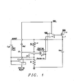
Fig. 1 shows the basic elements of a second embodiment of a start-up circuit of the present disclosure applied to a LDO. -
Fig. 2 illustrates a third embodiment of a start-up circuit of the present disclosure applied to a LDO. -
Fig. 3 illustrates a flowchart of a method to maintain a resistive voltage divider ratio during start-up of an electronic circuit comprising a feed-forward capacitor across a feedback resistor using a dynamic start-up circuit. -
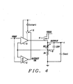
Fig. 4 shows basic elements of an embodiment of a start-up circuit of the present disclosure applied for example to a LDO. - Methods and circuits to achieve fast and clean start-up process of an electronic circuit as e.g. a LDO or an amplifier using a feed-forward capacitor and a resistive voltage divider or another means to represent an output voltage of the electronic circuit are disclosed. It has to be noted that the methods and circuits disclosed can be applied to any other circuits using a feed-forward capacitor and a resistive voltage divider.
-
Fig. 4 shows basic elements of an embodiment of a start-up circuit of the present disclosure applied for example to a LDO. The circuit comprises a port foroutput voltage 1, a resistor voltage divider comprising a first resistor R1 and a second controllable resistor R2, a start-up comparator 2, adifferential amplifier 3, having as inputs a reference input voltage Vref and the voltage of a voltage access point divider-in 6 of the voltage divider R1/R2, representing the output voltage Vout of the circuit as input, and apass transistor 4. During the start-up phase a current source ISTART provides an extra bias current to thedifferential amplifier 3. Aswitch 5 opens and hence deactivates the extra bias current ISTART when the start-up phase is finished. - The output of the start-
up comparator 2 indicates that the circuit as e.g. a LDO is now ready for loading, i.e. the output of thecomparator 2 triggers interrupting the extra bias current via switch 5.The feed-forward capacitor CFF modifies the resistor divider R1/R2 ratio - The circuit of
Fig. 4 may have the following disadvantages: - 1. Longer startup time
- 2.Startup specifications may not being met
- 3.Incorrect decision by startup comparator about the output voltage which
may impact system functionality if this output is used to load the output of the circuit - 4. Drop in voltage of the LDO (brown out).
-
Fig. 1 shows a second embodiment of a start-up circuit of the present disclosure overcoming the disadvantages cited above. The start-up circuit ofFig. 1 can also be applied for example to a LDO or to other circuits as amplifiers, etc... - The circuit disclosed comprises a port for
output voltage 1, a resistor voltage divider comprising in a preferred embodiment a first resistor R1 and a second controllable resistor R2, a start-up comparator 2, adifferential amplifier 3, having a reference input voltage Vref and the voltage of a voltage access point divider-in 6 of the voltage divider R1/R2, representing the output voltage Vout of the circuit as input, a start-up buffer 5, and apass transistor 4. - Each of the resistors R1 and R2 could be implemented by more than one resistor in series. Furthermore other resistive means than resistors could be implemented for the voltage divider as well, e.g. transistors (BJT or MOS) or diodes or FETS or MOS transistors connected as diodes.
- The output of the start-
up comparator 2, comparing voltage Vref with the voltage of the voltage access point divider-in 6 of the voltage divider R1/R2, indicates that the circuit, as e.g. a LDO, that a start-up phase is completed and is now ready for loading. Thecomparator 2 controls the duration of a biasing current Ibuf for the start-up buffer 5 via switch S3. Switch S3 opens after start-up is completed,i.e. comparator 2 detects that voltage Vref is equal to divider-in 6 voltage, switch S3 opens, biasing current Ibuf is interrupted and start-up time specification are met. - Furthermore the circuit comprises a capacitor Cext, at the output which may be deployed externally or internally to the circuit, and a feed-forward capacitor CFF, which is connected only after start-up phase is completed in parallel to the controllable resistor R2. Capacitor CFF is connected in parallel to the controllable resistor R2 via switch S2, which is closed after the start-up phase is completed. The
comparator 2 detects when the start-up phase is completed and activates the closing of switch S2. - Furthermore there may be an optional current source Istart providing an optional bias current to the
differential amplifier 3 during start-up, wherein the optional current source Istart may be activated by a switch S1, which is used only if the optional extra bias current is to be provided during the startup. Switch S1 is also optional, it is not required if no extra bias current to theamplifier 3 is required during start-up of the circuit. Switch S2 connects, after it is closed when the start-up phase is finished, a voltage access point of the voltage divider R1/R2 to a lower plate of the feed-forward capacitor CFF. - Furthermore it should be noted that voltages VDD1 and VDD2 can be the same or different.
- During startup the switch S3 is closed and switch S2 is open. The open switch S2 disconnects the feed-forward capacitor CFF from the resistor divider R1/R2 but the start-
up buffer 5 maintains the lower plate of feed-forward capacitor CFF to a same potential as the voltageaccess point divider_in 6 of the voltage divider R1/R2. Once the output voltage Vout reaches the desired voltage, switch S2 is closed and switch S3 is opened. The start-up buffer is then shut down. - The start-
up buffer 5 is a means to maintain the voltage level of the voltageaccess point divider_in 6 of the resistive voltage divider R1/R2 on the feed-forward capacitor without impacting the voltage divider ratio. Other means could be used for this purpose as well. It has to be noted that thestartup buffer 5 consumes power only during the start-up phase of the circuit. It does not add to the quiescent current consumption of the circuit. -
Fig. 2 illustrates a third embodiment of a start-up circuit of the present disclosure applied to a LDO. Similarly to the circuit shown inFig. 1 the circuit ofFig. 2 comprises also adifferential amplifier 3, a start-upcomparator 2, apass transistor 4, and a voltage divider R1/R2 with a the voltageaccess point divider_in 6. Thedifferential amplifier 3 may have a fixed or variable reference voltage as first input and the voltage of the voltageaccess point divider_in 6 as second input. As shown inFig. 1 the start-upcomparator 2 detects when the start-up phase is completed. The resistors R1/R2 may have a fixed resistance, or both a controllable resistance, or a combination thereof. - This implementation is characterized by having a start-up capacitor CFF2 connected during the start-up phase in series with the feed-forward capacitor CFF and in parallel to resistor R1, i.e. the resistive voltage divider R1/R2 and the capacitor string CFF/CFF2 are in parallel, while a mid-point of the capacitor string is connected to the voltage
access point divider_in 6 of the resistive divider R1/R2. - A key point of the circuit of
Fig. 2 is that the start-up capacitor CFF2 is disconnected by switch S4 at the end of the start-up phase, which is triggered by the start-upcomparator 2. - The start-up capacitor CEFF2 has a capacitance of CFFxR2/R1, i.e. the capacitive string has capacitances according to the resistances of the resistive voltage divider R1/R2. Thus CFF2 prevents any modification of the resistive voltage divider ratio by the feed-forward capacitor CFF during start-up.
- Similarly to the circuit shown in
Fig. 1 a start-upcomparator 2 monitors if the output voltage has reached a desired level and if the start-up phase is finished and the desired output level has been reached the start-up comparator activates that switch S4 is opened and hence the additional capacitor CEFF2 is disconnected. - Furthermore there may be an optional current source Istart providing an optional extra bias current to the
differential amplifier 3 during start-up, wherein the optional current source Istart may be activated by a switch S5, which is used only if the optional extra bias current is to be provided during the startup to thedifferential amplifier 3. Switch S5 is also optional, it is not required if no extra bias current to theamplifier 3 is required during start-up of the circuit. - The embodiment of
Fig. 2 does not require, compared to the circuit ofFig. 1 , a start-upbuffer amplifier 5 and switches S2 and S3 as shown inFig. 1 , but it requires switch S4 and the additional capacitor CEFF2, which will be disconnected by switch S4 after start-up is completed. - Similarly to the circuit of
Fig. 1 the circuit ofFig. 2 may comprise a capacitor Cext, at the output which may be deployed externally or internally to the circuit. - In alternative embodiments of the circuits of
Figs. 1 orFig. 2 the reference input voltage Vref, as shown inFig. 1 andFig. 2 , may be replaced by a variable voltage Vin or both resistors R1 and R2 are controllable. Alternatively it would be possible to have a fixed resistance for R2 and a controllable resistance for R1. -
Fig. 3 illustrates a flowchart of a method to maintain a resistive voltage divider ratio during start-up of an electronic circuit such as a LDO, amplifier, or buffer comprising a feed-forward capacitor across a feedback resistor using a dynamic start-up circuit. As already mentioned above, the circuit and the method disclosed are applicable to any circuit using a resistive voltage divider and a feed-forward capacitor.Step 30 of the method ofFig. 3 illustrates the provision of e.g. a LDO or any other suitable circuit as e.g. an amplifier comprising a feed-forward capacitor across a first feedback resistor R2 of a resistive voltage divider and a start-up circuit.Step 31 depicts avoiding modification of resistive voltage divider ratio caused by feed-forward capacitor during start-up phase.Step 32 illustrates monitoring output voltage and finish start-up-phase when desired output voltage of the electronic circuit is reached.Step 33 shows processing normal operation after start-up phase is finished wherein feed-forward capacitor is connected across the feedback resistor of the resistive voltage after end of start-up phase. - While the disclosure has been particularly shown and described with reference to the preferred embodiments thereof, it will be understood by those skilled in the art that various changes in form and details may be made without departing from the spirit and scope of the disclosure.
Claims (19)
- A method to maintain a resistive voltage divider ratio during start-up of any electronic circuit comprising a feed-forward capacitor across a feedback resistor of a resistive voltage divider using a dynamic start-up circuit, comprising the following steps:(1) providing an electronic circuit comprising a feed-forward capacitor across a first feedback resistor of a resistive voltage divider and a start-up circuit;(2) avoiding modification of resistive voltage divider ratio caused by feed-forward capacitor during start-up phase;(3) monitoring output voltage and finish start-up-phase when desired output voltage of the electronic circuit is reached; and(4) processing normal operation after start-up phase is finished wherein feed-forward capacitor is connected across the feedback resistor of the resistive voltage divider after end of start-up phase.
- The method of claim 1 wherein said electronic circuit is a LDO or an amplifier.
- The method of claim 1 wherein a start-up comparator detects if a desired output voltage is reached and hence the start-up phase is finished.
- The method of claim 3 wherein the start-up comparator detects if the start-up phase is finished by comparing a voltage representing the output voltage of the electronic circuit with a reference voltage, e.g. a variable voltage.
- The method of claim 1 wherein said modification of resistive voltage divider ratio is avoided by disconnecting the feed-forward capacitor from a voltage access point of the resistive voltage divider during start-up phase only, wherein the voltage of the voltage access point of the resistive voltage divider represents the output voltage of the electronic circuit.
- The method of claim 1 wherein a voltage level of the voltage access point of the resistive voltage divider is maintained on the feed-forward capacitor by a start-up buffer during start-up phase, wherein the voltage of the voltage access point of the resistive voltage divider represents the output voltage of the electronic circuit and wherein a bias current of the buffer amplifier is disconnected at the end of the start-up phase, wherein an input of the start-up buffer is connected to the voltage access point of the voltage divider.
- The method of claim 6 wherein a start-up comparator detects if a desired output voltage of the electronic circuit is reached and, in this case, initiates disconnecting the bias current of the start-up buffer and connecting the feed-forward capacitor directly to the voltage access point of the resistive voltage divider.
- The method of claim 1 wherein said modification of resistive voltage divider ratio is prevented by connecting a start-up capacitor across a second resistor of the resistive voltage divider during the start-up phase only, wherein the start-up capacitor has a capacitance of CFF x R2/R1, wherein CFF is a capacitance of the feed-forward capacitor, R1 is a resistance of the part of the voltage divider between access point and ground and R2 is a resistance of the part of the voltage diver between output voltage and access point.
- The method of claim 8 wherein a start-up comparator detects if a desired output voltage is reached and, in this case, disconnects the start-up capacitor from the voltage access point of the voltage divider.
- The method of claim 8 wherein the start-up capacitor has a capacitance of CFF x R2/R1, wherein CFF is a capacitance of the feed-forward capacitor, R1 is a resistance of a part of the voltage divider between a voltage access point of the resistive voltage divider and ground and R2 is a resistance of the part of the voltage divider between output voltage and access point.
- The method of claim 1 wherein said first feedback resistor is a part of the resistive voltage divider.
- A circuit to maintain a resistive voltage divider ratio during start-up of any electronic circuit comprising a feed-forward capacitor across a feedback resistor and a resistive voltage divider using a dynamic start-up circuit, comprising:- the feed-forward capacitor, wherein a first plate of the feed-forward capacitor is connected to an output port of the circuit and a second plate is connected to a voltage access point of the resistive voltage divider after the start-up phase of the electronic circuit is finished;- said resistive voltage divider, being connected between an output port of the circuit and ground, comprising the feedback resistor having a resistance R2 connected between the output port of the circuit and the voltage access point in-between the voltage divider having a fraction of the output voltage and further comprising a second resistor having a resistance R1;- a start-up comparator detecting if the start-up phase is finished by comparing a voltage representing the output voltage of the electronic circuit with a reference voltage;- a means to maintain a voltage level of the voltage access point across the feed-forward capacitor during start-up of the circuit, wherein the means to maintain a voltage level of the voltage access point comprises switching means to connect or disconnect components of the circuit at beginning and end of the start-up process, wherein the switching means are activated by the start-up comparator.
- The circuit of claim 12 wherein said circuit is an LDO or an amplifier.
- The circuit of claim 12 wherein the end of the start-up phase is reached when the voltage of the voltage access point equals a reference voltage, e.g. either a fixed voltage or a variable voltage.
- The circuit of claim 12 wherein said means to maintain the voltage level further comprises a buffer amplifier wherein the start-up comparator initiates both connecting a second plate of the feed-forward capacitor to the voltage access point and disconnecting a bias current of the buffer amplifier at the end of the start-up phase using said switching means, wherein an input of the start-up buffer is connected to the voltage access point of the voltage divider.
- The circuit of claim 15 wherein said switching means comprises a first switching means connecting the second plate of the feed-forward capacitor to the voltage access point at the end of the start-up phase and a second switching means disconnecting the bias current of the buffer amplifier.
- The circuit of claim 16 wherein said switching means further comprises a third switching means providing an extra bias current to a differential amplifier of the circuit during start-up only.
- The circuit of claim 12 wherein said means to maintain the voltage level comprises a second capacitor connected between the voltage access point and ground.
- The circuit of claim 18 wherein the second capacitor has a capacitance C = CFFxR2/R1, wherein CFF is the capacitance of the feed-forward capacitor and wherein the start-up comparator initiates disconnecting the second capacitor from the voltage access point via a switching means at the end of the start-up phase.
Priority Applications (3)
| Application Number | Priority Date | Filing Date | Title |
|---|---|---|---|
| EP13392001.7A EP2759900B1 (en) | 2013-01-25 | 2013-01-25 | Maintaining the resistor divider ratio during start-up |
| US13/756,568 US20140210430A1 (en) | 2013-01-25 | 2013-02-01 | Maintaining the Resistor Divider Ratio During Start-up |
| US14/794,135 US9372491B2 (en) | 2013-01-25 | 2015-07-08 | Maintaining the resistor divider ratio during start-up |
Applications Claiming Priority (1)
| Application Number | Priority Date | Filing Date | Title |
|---|---|---|---|
| EP13392001.7A EP2759900B1 (en) | 2013-01-25 | 2013-01-25 | Maintaining the resistor divider ratio during start-up |
Publications (2)
| Publication Number | Publication Date |
|---|---|
| EP2759900A1 true EP2759900A1 (en) | 2014-07-30 |
| EP2759900B1 EP2759900B1 (en) | 2017-11-22 |
Family
ID=47740883
Family Applications (1)
| Application Number | Title | Priority Date | Filing Date |
|---|---|---|---|
| EP13392001.7A Active EP2759900B1 (en) | 2013-01-25 | 2013-01-25 | Maintaining the resistor divider ratio during start-up |
Country Status (2)
| Country | Link |
|---|---|
| US (2) | US20140210430A1 (en) |
| EP (1) | EP2759900B1 (en) |
Cited By (1)
| Publication number | Priority date | Publication date | Assignee | Title |
|---|---|---|---|---|
| EP3451111A1 (en) * | 2017-08-30 | 2019-03-06 | Renesas Electronics Corporation | Semiconductor device, signal processing system, and signal processing method |
Families Citing this family (10)
| Publication number | Priority date | Publication date | Assignee | Title |
|---|---|---|---|---|
| EP2846213B1 (en) * | 2013-09-05 | 2023-05-03 | Renesas Design Germany GmbH | Method and apparatus for limiting startup inrush current for low dropout regulator |
| JP6454169B2 (en) * | 2015-02-04 | 2019-01-16 | エイブリック株式会社 | Voltage regulator |
| US9588540B2 (en) * | 2015-09-10 | 2017-03-07 | Freescale Semiconductor, Inc. | Supply-side voltage regulator |
| US10768646B2 (en) * | 2017-03-09 | 2020-09-08 | Macronix International Co., Ltd. | Low dropout regulating device and operating method thereof |
| DE102017205957B4 (en) * | 2017-04-07 | 2022-12-29 | Dialog Semiconductor (Uk) Limited | CIRCUIT AND METHOD FOR QUICK CURRENT CONTROL IN VOLTAGE REGULATORS |
| DE102019202853B3 (en) | 2019-03-01 | 2020-06-18 | Dialog Semiconductor (Uk) Limited | Linear voltage regulator and method for voltage regulation |
| US11296596B1 (en) * | 2021-02-18 | 2022-04-05 | Nxp B.V. | Noise reduction circuit for voltage regulator |
| US20240012438A1 (en) * | 2022-07-05 | 2024-01-11 | Mediatek Inc. | Electronic system using a power regulator with reduced inrush current |
| TWI850915B (en) * | 2022-12-21 | 2024-08-01 | 大陸商星宸科技股份有限公司 | Digital circuitry and power supply method |
| CN117369576A (en) * | 2023-11-10 | 2024-01-09 | 西安紫光国芯半导体股份有限公司 | A voltage regulator, power management chip and module device |
Citations (4)
| Publication number | Priority date | Publication date | Assignee | Title |
|---|---|---|---|---|
| US6208124B1 (en) * | 1999-06-04 | 2001-03-27 | Matsushita Electric Industrial Co., Ltd. | Semiconductor integrated circuit |
| US7122996B1 (en) * | 2004-06-01 | 2006-10-17 | National Semiconductor Corporation | Voltage regulator circuit |
| WO2011090687A2 (en) * | 2010-01-22 | 2011-07-28 | Texas Instruments Incorporated | Low-power feedback and method for dc-dc converters and voltage regulators for energy harvesters |
| US20110291636A1 (en) * | 2010-05-28 | 2011-12-01 | Minoru Sudou | Voltage regulator |
Family Cites Families (6)
| Publication number | Priority date | Publication date | Assignee | Title |
|---|---|---|---|---|
| US7872454B2 (en) | 2003-08-21 | 2011-01-18 | Marvell World Trade Ltd. | Digital low dropout regulator |
| FR2872305B1 (en) | 2004-06-24 | 2006-09-22 | St Microelectronics Sa | METHOD FOR CONTROLLING THE OPERATION OF A LOW VOLTAGE DROP REGULATOR AND CORRESPONDING INTEGRATED CIRCUIT |
| US7531996B2 (en) | 2006-11-21 | 2009-05-12 | System General Corp. | Low dropout regulator with wide input voltage range |
| US9411348B2 (en) * | 2010-04-13 | 2016-08-09 | Semiconductor Components Industries, Llc | Programmable low-dropout regulator and methods therefor |
| JP2013012000A (en) * | 2011-06-29 | 2013-01-17 | Mitsumi Electric Co Ltd | Semiconductor integrated circuit for regulator |
| US8710811B2 (en) * | 2012-01-03 | 2014-04-29 | Nan Ya Technology Corporation | Voltage regulator with improved voltage regulator response and reduced voltage drop |
-
2013
- 2013-01-25 EP EP13392001.7A patent/EP2759900B1/en active Active
- 2013-02-01 US US13/756,568 patent/US20140210430A1/en not_active Abandoned
-
2015
- 2015-07-08 US US14/794,135 patent/US9372491B2/en active Active
Patent Citations (4)
| Publication number | Priority date | Publication date | Assignee | Title |
|---|---|---|---|---|
| US6208124B1 (en) * | 1999-06-04 | 2001-03-27 | Matsushita Electric Industrial Co., Ltd. | Semiconductor integrated circuit |
| US7122996B1 (en) * | 2004-06-01 | 2006-10-17 | National Semiconductor Corporation | Voltage regulator circuit |
| WO2011090687A2 (en) * | 2010-01-22 | 2011-07-28 | Texas Instruments Incorporated | Low-power feedback and method for dc-dc converters and voltage regulators for energy harvesters |
| US20110291636A1 (en) * | 2010-05-28 | 2011-12-01 | Minoru Sudou | Voltage regulator |
Cited By (2)
| Publication number | Priority date | Publication date | Assignee | Title |
|---|---|---|---|---|
| EP3451111A1 (en) * | 2017-08-30 | 2019-03-06 | Renesas Electronics Corporation | Semiconductor device, signal processing system, and signal processing method |
| US10461766B2 (en) | 2017-08-30 | 2019-10-29 | Renesas Electronics Corporation | Semiconductor device, signal processing system, and signal processing method |
Also Published As
| Publication number | Publication date |
|---|---|
| US20140210430A1 (en) | 2014-07-31 |
| US20150309520A1 (en) | 2015-10-29 |
| US9372491B2 (en) | 2016-06-21 |
| EP2759900B1 (en) | 2017-11-22 |
Similar Documents
| Publication | Publication Date | Title |
|---|---|---|
| EP2759900B1 (en) | Maintaining the resistor divider ratio during start-up | |
| CN101814833B (en) | Voltage regulator | |
| US8575903B2 (en) | Voltage regulator that can operate with or without an external power transistor | |
| EP3311235B1 (en) | Low-dropout voltage regulator apparatus | |
| US20160357206A1 (en) | Ldo regulator with improved load transient performance for internal power supply | |
| US9958889B2 (en) | High and low power voltage regulation circuit | |
| US9740221B2 (en) | Method to limit the inrush current in large output capacitance LDO's | |
| US9455628B2 (en) | Voltage regulator with overshoot suppression circuit and capability to stop overshoot suppression | |
| US9395731B2 (en) | Circuit to reduce output capacitor of LDOs | |
| US9058048B2 (en) | Voltage regulator having error amplifier | |
| US7602161B2 (en) | Voltage regulator with inherent voltage clamping | |
| CN104750150A (en) | Regulators and Electronics | |
| JP6454169B2 (en) | Voltage regulator | |
| KR20170123249A (en) | Dcdc converter | |
| US11294412B2 (en) | Apparatuses and methods involving switching between dual inputs of power amplification circuitry | |
| TW201908905A (en) | Switching controller and method for load | |
| KR20100077804A (en) | Boost operational amplifier | |
| US9910811B2 (en) | Hot swap circuit | |
| US9166468B2 (en) | Voltage regulator circuit with soft-start function | |
| US10459465B2 (en) | Power-down discharger | |
| US8405460B2 (en) | Circuitry for biasing amplifiers | |
| US8854097B2 (en) | Load switch | |
| EP2759899A1 (en) | Clean startup and power saving in pulsed enabling of LDO | |
| TWI405067B (en) | Control circuit for negative voltage regulator and method for controlling negative voltage regulator | |
| TW201823908A (en) | Voltage dividers |
Legal Events
| Date | Code | Title | Description |
|---|---|---|---|
| PUAI | Public reference made under article 153(3) epc to a published international application that has entered the european phase |
Free format text: ORIGINAL CODE: 0009012 |
|
| 17P | Request for examination filed |
Effective date: 20130125 |
|
| AK | Designated contracting states |
Kind code of ref document: A1 Designated state(s): AL AT BE BG CH CY CZ DE DK EE ES FI FR GB GR HR HU IE IS IT LI LT LU LV MC MK MT NL NO PL PT RO RS SE SI SK SM TR |
|
| AX | Request for extension of the european patent |
Extension state: BA ME |
|
| R17P | Request for examination filed (corrected) |
Effective date: 20150129 |
|
| RBV | Designated contracting states (corrected) |
Designated state(s): AL AT BE BG CH CY CZ DE DK EE ES FI FR GB GR HR HU IE IS IT LI LT LU LV MC MK MT NL NO PL PT RO RS SE SI SK SM TR |
|
| REG | Reference to a national code |
Ref country code: DE Ref legal event code: R079 Ref document number: 602013029726 Country of ref document: DE Free format text: PREVIOUS MAIN CLASS: G05F0001575000 Ipc: G05F0003020000 |
|
| GRAP | Despatch of communication of intention to grant a patent |
Free format text: ORIGINAL CODE: EPIDOSNIGR1 |
|
| RIC1 | Information provided on ipc code assigned before grant |
Ipc: G05F 3/02 20060101AFI20170428BHEP |
|
| INTG | Intention to grant announced |
Effective date: 20170530 |
|
| RIN1 | Information on inventor provided before grant (corrected) |
Inventor name: LUDMIL, NIKOLOV Inventor name: AMBREESH, BHATTAD |
|
| GRAS | Grant fee paid |
Free format text: ORIGINAL CODE: EPIDOSNIGR3 |
|
| GRAA | (expected) grant |
Free format text: ORIGINAL CODE: 0009210 |
|
| AK | Designated contracting states |
Kind code of ref document: B1 Designated state(s): AL AT BE BG CH CY CZ DE DK EE ES FI FR GB GR HR HU IE IS IT LI LT LU LV MC MK MT NL NO PL PT RO RS SE SI SK SM TR |
|
| REG | Reference to a national code |
Ref country code: GB Ref legal event code: FG4D |
|
| REG | Reference to a national code |
Ref country code: CH Ref legal event code: EP |
|
| REG | Reference to a national code |
Ref country code: IE Ref legal event code: FG4D |
|
| REG | Reference to a national code |
Ref country code: AT Ref legal event code: REF Ref document number: 948958 Country of ref document: AT Kind code of ref document: T Effective date: 20171215 |
|
| REG | Reference to a national code |
Ref country code: DE Ref legal event code: R096 Ref document number: 602013029726 Country of ref document: DE |
|
| REG | Reference to a national code |
Ref country code: NL Ref legal event code: MP Effective date: 20171122 |
|
| REG | Reference to a national code |
Ref country code: LT Ref legal event code: MG4D |
|
| REG | Reference to a national code |
Ref country code: AT Ref legal event code: MK05 Ref document number: 948958 Country of ref document: AT Kind code of ref document: T Effective date: 20171122 |
|
| PG25 | Lapsed in a contracting state [announced via postgrant information from national office to epo] |
Ref country code: NL Free format text: LAPSE BECAUSE OF FAILURE TO SUBMIT A TRANSLATION OF THE DESCRIPTION OR TO PAY THE FEE WITHIN THE PRESCRIBED TIME-LIMIT Effective date: 20171122 Ref country code: ES Free format text: LAPSE BECAUSE OF FAILURE TO SUBMIT A TRANSLATION OF THE DESCRIPTION OR TO PAY THE FEE WITHIN THE PRESCRIBED TIME-LIMIT Effective date: 20171122 Ref country code: FI Free format text: LAPSE BECAUSE OF FAILURE TO SUBMIT A TRANSLATION OF THE DESCRIPTION OR TO PAY THE FEE WITHIN THE PRESCRIBED TIME-LIMIT Effective date: 20171122 Ref country code: SE Free format text: LAPSE BECAUSE OF FAILURE TO SUBMIT A TRANSLATION OF THE DESCRIPTION OR TO PAY THE FEE WITHIN THE PRESCRIBED TIME-LIMIT Effective date: 20171122 Ref country code: LT Free format text: LAPSE BECAUSE OF FAILURE TO SUBMIT A TRANSLATION OF THE DESCRIPTION OR TO PAY THE FEE WITHIN THE PRESCRIBED TIME-LIMIT Effective date: 20171122 Ref country code: NO Free format text: LAPSE BECAUSE OF FAILURE TO SUBMIT A TRANSLATION OF THE DESCRIPTION OR TO PAY THE FEE WITHIN THE PRESCRIBED TIME-LIMIT Effective date: 20180222 |
|
| PG25 | Lapsed in a contracting state [announced via postgrant information from national office to epo] |
Ref country code: HR Free format text: LAPSE BECAUSE OF FAILURE TO SUBMIT A TRANSLATION OF THE DESCRIPTION OR TO PAY THE FEE WITHIN THE PRESCRIBED TIME-LIMIT Effective date: 20171122 Ref country code: LV Free format text: LAPSE BECAUSE OF FAILURE TO SUBMIT A TRANSLATION OF THE DESCRIPTION OR TO PAY THE FEE WITHIN THE PRESCRIBED TIME-LIMIT Effective date: 20171122 Ref country code: RS Free format text: LAPSE BECAUSE OF FAILURE TO SUBMIT A TRANSLATION OF THE DESCRIPTION OR TO PAY THE FEE WITHIN THE PRESCRIBED TIME-LIMIT Effective date: 20171122 Ref country code: AT Free format text: LAPSE BECAUSE OF FAILURE TO SUBMIT A TRANSLATION OF THE DESCRIPTION OR TO PAY THE FEE WITHIN THE PRESCRIBED TIME-LIMIT Effective date: 20171122 Ref country code: GR Free format text: LAPSE BECAUSE OF FAILURE TO SUBMIT A TRANSLATION OF THE DESCRIPTION OR TO PAY THE FEE WITHIN THE PRESCRIBED TIME-LIMIT Effective date: 20180223 Ref country code: BG Free format text: LAPSE BECAUSE OF FAILURE TO SUBMIT A TRANSLATION OF THE DESCRIPTION OR TO PAY THE FEE WITHIN THE PRESCRIBED TIME-LIMIT Effective date: 20180222 |
|
| PG25 | Lapsed in a contracting state [announced via postgrant information from national office to epo] |
Ref country code: CY Free format text: LAPSE BECAUSE OF FAILURE TO SUBMIT A TRANSLATION OF THE DESCRIPTION OR TO PAY THE FEE WITHIN THE PRESCRIBED TIME-LIMIT Effective date: 20171122 Ref country code: EE Free format text: LAPSE BECAUSE OF FAILURE TO SUBMIT A TRANSLATION OF THE DESCRIPTION OR TO PAY THE FEE WITHIN THE PRESCRIBED TIME-LIMIT Effective date: 20171122 Ref country code: CZ Free format text: LAPSE BECAUSE OF FAILURE TO SUBMIT A TRANSLATION OF THE DESCRIPTION OR TO PAY THE FEE WITHIN THE PRESCRIBED TIME-LIMIT Effective date: 20171122 Ref country code: SK Free format text: LAPSE BECAUSE OF FAILURE TO SUBMIT A TRANSLATION OF THE DESCRIPTION OR TO PAY THE FEE WITHIN THE PRESCRIBED TIME-LIMIT Effective date: 20171122 Ref country code: DK Free format text: LAPSE BECAUSE OF FAILURE TO SUBMIT A TRANSLATION OF THE DESCRIPTION OR TO PAY THE FEE WITHIN THE PRESCRIBED TIME-LIMIT Effective date: 20171122 |
|
| REG | Reference to a national code |
Ref country code: DE Ref legal event code: R097 Ref document number: 602013029726 Country of ref document: DE |
|
| PG25 | Lapsed in a contracting state [announced via postgrant information from national office to epo] |
Ref country code: PL Free format text: LAPSE BECAUSE OF FAILURE TO SUBMIT A TRANSLATION OF THE DESCRIPTION OR TO PAY THE FEE WITHIN THE PRESCRIBED TIME-LIMIT Effective date: 20171122 Ref country code: SM Free format text: LAPSE BECAUSE OF FAILURE TO SUBMIT A TRANSLATION OF THE DESCRIPTION OR TO PAY THE FEE WITHIN THE PRESCRIBED TIME-LIMIT Effective date: 20171122 Ref country code: RO Free format text: LAPSE BECAUSE OF FAILURE TO SUBMIT A TRANSLATION OF THE DESCRIPTION OR TO PAY THE FEE WITHIN THE PRESCRIBED TIME-LIMIT Effective date: 20171122 Ref country code: IT Free format text: LAPSE BECAUSE OF FAILURE TO SUBMIT A TRANSLATION OF THE DESCRIPTION OR TO PAY THE FEE WITHIN THE PRESCRIBED TIME-LIMIT Effective date: 20171122 |
|
| REG | Reference to a national code |
Ref country code: CH Ref legal event code: PL |
|
| PLBE | No opposition filed within time limit |
Free format text: ORIGINAL CODE: 0009261 |
|
| STAA | Information on the status of an ep patent application or granted ep patent |
Free format text: STATUS: NO OPPOSITION FILED WITHIN TIME LIMIT |
|
| 26N | No opposition filed |
Effective date: 20180823 |
|
| PG25 | Lapsed in a contracting state [announced via postgrant information from national office to epo] |
Ref country code: LU Free format text: LAPSE BECAUSE OF NON-PAYMENT OF DUE FEES Effective date: 20180125 Ref country code: FR Free format text: LAPSE BECAUSE OF NON-PAYMENT OF DUE FEES Effective date: 20180131 |
|
| REG | Reference to a national code |
Ref country code: IE Ref legal event code: MM4A |
|
| REG | Reference to a national code |
Ref country code: FR Ref legal event code: ST Effective date: 20180928 |
|
| REG | Reference to a national code |
Ref country code: BE Ref legal event code: MM Effective date: 20180131 |
|
| PG25 | Lapsed in a contracting state [announced via postgrant information from national office to epo] |
Ref country code: SI Free format text: LAPSE BECAUSE OF FAILURE TO SUBMIT A TRANSLATION OF THE DESCRIPTION OR TO PAY THE FEE WITHIN THE PRESCRIBED TIME-LIMIT Effective date: 20171122 Ref country code: BE Free format text: LAPSE BECAUSE OF NON-PAYMENT OF DUE FEES Effective date: 20180131 Ref country code: CH Free format text: LAPSE BECAUSE OF NON-PAYMENT OF DUE FEES Effective date: 20180131 Ref country code: LI Free format text: LAPSE BECAUSE OF NON-PAYMENT OF DUE FEES Effective date: 20180131 |
|
| PG25 | Lapsed in a contracting state [announced via postgrant information from national office to epo] |
Ref country code: IE Free format text: LAPSE BECAUSE OF NON-PAYMENT OF DUE FEES Effective date: 20180125 |
|
| PG25 | Lapsed in a contracting state [announced via postgrant information from national office to epo] |
Ref country code: MC Free format text: LAPSE BECAUSE OF FAILURE TO SUBMIT A TRANSLATION OF THE DESCRIPTION OR TO PAY THE FEE WITHIN THE PRESCRIBED TIME-LIMIT Effective date: 20171122 |
|
| PG25 | Lapsed in a contracting state [announced via postgrant information from national office to epo] |
Ref country code: MT Free format text: LAPSE BECAUSE OF NON-PAYMENT OF DUE FEES Effective date: 20180125 |
|
| PG25 | Lapsed in a contracting state [announced via postgrant information from national office to epo] |
Ref country code: TR Free format text: LAPSE BECAUSE OF FAILURE TO SUBMIT A TRANSLATION OF THE DESCRIPTION OR TO PAY THE FEE WITHIN THE PRESCRIBED TIME-LIMIT Effective date: 20171122 |
|
| PG25 | Lapsed in a contracting state [announced via postgrant information from national office to epo] |
Ref country code: HU Free format text: LAPSE BECAUSE OF FAILURE TO SUBMIT A TRANSLATION OF THE DESCRIPTION OR TO PAY THE FEE WITHIN THE PRESCRIBED TIME-LIMIT; INVALID AB INITIO Effective date: 20130125 Ref country code: PT Free format text: LAPSE BECAUSE OF FAILURE TO SUBMIT A TRANSLATION OF THE DESCRIPTION OR TO PAY THE FEE WITHIN THE PRESCRIBED TIME-LIMIT Effective date: 20171122 |
|
| PG25 | Lapsed in a contracting state [announced via postgrant information from national office to epo] |
Ref country code: MK Free format text: LAPSE BECAUSE OF NON-PAYMENT OF DUE FEES Effective date: 20171122 |
|
| PG25 | Lapsed in a contracting state [announced via postgrant information from national office to epo] |
Ref country code: AL Free format text: LAPSE BECAUSE OF FAILURE TO SUBMIT A TRANSLATION OF THE DESCRIPTION OR TO PAY THE FEE WITHIN THE PRESCRIBED TIME-LIMIT Effective date: 20171122 Ref country code: IS Free format text: LAPSE BECAUSE OF FAILURE TO SUBMIT A TRANSLATION OF THE DESCRIPTION OR TO PAY THE FEE WITHIN THE PRESCRIBED TIME-LIMIT Effective date: 20180322 |
|
| REG | Reference to a national code |
Ref country code: DE Ref legal event code: R082 Ref document number: 602013029726 Country of ref document: DE |
|
| PGFP | Annual fee paid to national office [announced via postgrant information from national office to epo] |
Ref country code: GB Payment date: 20260113 Year of fee payment: 14 |
|
| PGFP | Annual fee paid to national office [announced via postgrant information from national office to epo] |
Ref country code: DE Payment date: 20260108 Year of fee payment: 14 |