EP2758831B1 - Backlight device - Google Patents
Backlight device Download PDFInfo
- Publication number
- EP2758831B1 EP2758831B1 EP12769747.2A EP12769747A EP2758831B1 EP 2758831 B1 EP2758831 B1 EP 2758831B1 EP 12769747 A EP12769747 A EP 12769747A EP 2758831 B1 EP2758831 B1 EP 2758831B1
- Authority
- EP
- European Patent Office
- Prior art keywords
- prism
- face
- backlight device
- film
- normal line
- Prior art date
- Legal status (The legal status is an assumption and is not a legal conclusion. Google has not performed a legal analysis and makes no representation as to the accuracy of the status listed.)
- Not-in-force
Links
Images


Classifications
-
- G—PHYSICS
- G02—OPTICS
- G02B—OPTICAL ELEMENTS, SYSTEMS OR APPARATUS
- G02B6/00—Light guides; Structural details of arrangements comprising light guides and other optical elements, e.g. couplings
- G02B6/0001—Light guides; Structural details of arrangements comprising light guides and other optical elements, e.g. couplings specially adapted for lighting devices or systems
- G02B6/0011—Light guides; Structural details of arrangements comprising light guides and other optical elements, e.g. couplings specially adapted for lighting devices or systems the light guides being planar or of plate-like form
- G02B6/0033—Means for improving the coupling-out of light from the light guide
- G02B6/005—Means for improving the coupling-out of light from the light guide provided by one optical element, or plurality thereof, placed on the light output side of the light guide
- G02B6/0053—Prismatic sheet or layer; Brightness enhancement element, sheet or layer
-
- G—PHYSICS
- G02—OPTICS
- G02B—OPTICAL ELEMENTS, SYSTEMS OR APPARATUS
- G02B5/00—Optical elements other than lenses
- G02B5/04—Prisms
- G02B5/045—Prism arrays
-
- G—PHYSICS
- G02—OPTICS
- G02F—OPTICAL DEVICES OR ARRANGEMENTS FOR THE CONTROL OF LIGHT BY MODIFICATION OF THE OPTICAL PROPERTIES OF THE MEDIA OF THE ELEMENTS INVOLVED THEREIN; NON-LINEAR OPTICS; FREQUENCY-CHANGING OF LIGHT; OPTICAL LOGIC ELEMENTS; OPTICAL ANALOGUE/DIGITAL CONVERTERS
- G02F1/00—Devices or arrangements for the control of the intensity, colour, phase, polarisation or direction of light arriving from an independent light source, e.g. switching, gating or modulating; Non-linear optics
- G02F1/01—Devices or arrangements for the control of the intensity, colour, phase, polarisation or direction of light arriving from an independent light source, e.g. switching, gating or modulating; Non-linear optics for the control of the intensity, phase, polarisation or colour
- G02F1/13—Devices or arrangements for the control of the intensity, colour, phase, polarisation or direction of light arriving from an independent light source, e.g. switching, gating or modulating; Non-linear optics for the control of the intensity, phase, polarisation or colour based on liquid crystals, e.g. single liquid crystal display cells
- G02F1/133—Constructional arrangements; Operation of liquid crystal cells; Circuit arrangements
- G02F1/1333—Constructional arrangements; Manufacturing methods
- G02F1/1335—Structural association of cells with optical devices, e.g. polarisers or reflectors
- G02F1/1336—Illuminating devices
- G02F1/133615—Edge-illuminating devices, i.e. illuminating from the side
-
- G—PHYSICS
- G02—OPTICS
- G02B—OPTICAL ELEMENTS, SYSTEMS OR APPARATUS
- G02B6/00—Light guides; Structural details of arrangements comprising light guides and other optical elements, e.g. couplings
- G02B6/0001—Light guides; Structural details of arrangements comprising light guides and other optical elements, e.g. couplings specially adapted for lighting devices or systems
- G02B6/0011—Light guides; Structural details of arrangements comprising light guides and other optical elements, e.g. couplings specially adapted for lighting devices or systems the light guides being planar or of plate-like form
- G02B6/0033—Means for improving the coupling-out of light from the light guide
- G02B6/005—Means for improving the coupling-out of light from the light guide provided by one optical element, or plurality thereof, placed on the light output side of the light guide
- G02B6/0055—Reflecting element, sheet or layer
Definitions
- An aspect of the present invention is related to a backlight device for use in display devices.
- a backlight device including a light guide unit, a light source disposed on at least one end of the light guide unit, and reflection means disposed on a bottom face of the light guide unit that reflect light from the light guide unit (e.g. JP2000-214460A ).
- the reflection means form a triangular shape having a ridge line formed by an apex angle in a direction substantially parallel to the light entrance face of the light guide unit.
- a plurality of the apex angle is formed uniformly in a direction substantially perpendicular to the light entrance face of the light guide unit.
- US 2009/0290098 A1 describes a reflection sheet that is used together with a prismatic light guide plate for the backlight of a liquid crystal display device, wherein a prism layer is formed on one surface of a reflection sheet, the vertex angle of the prisms is 145° or greater and 168° or less, and the distance between the vertices of the prisms on the reflection sheet is 50 ⁇ m or greater and 550 ⁇ m or less, and the reflection sheet is arranged in such a way that the prism array direction of the reflection sheet makes an angle of 5° or greater and 20° or less with respect to the prism array direction of the prismatic light guide plate.
- WO 2009/085543 A1 describes a back reflector for a light guide in a turning film backlight including a prism film layer in direct contact with a reflective layer.
- US 5,966,192 A discloses a surface light source device whose bright surface is excellent in whiteness and softness and a liquid crystal display that ensures a high visual quality.
- a backlight including a light source and one or more light recycling films is disclosed.
- the reflection means (reflector plate) described, for example, in JP2000-214460A , are used with at least one prism film, thereby making it possible to enhance light recycling and obtain a higher luminance.
- the light that has traveled from the reflector plate to the prism film along the direction substantially normal to the display panel returns to the reflector plate as a result of total reflection at the prism film, and then travels again from the reflector plate to the prism film along the direction normal to the display panel. It is possible that the process described above will repeat numerous times before the angle of incidence of the light with respect to the prism film escapes the range of total reflection. Therefore, it is possible that the light will travel back and forth numerous times between the reflector plate and the prism film.
- a backlight device is defined by the subject-matter of claim 1.
- an angle formed by the projected first and second normal line axes may be from 5 to 85 degrees.
- the angle formed by the projected first and second normal line axes may be not less than 25 degrees.
- a light guide provided so as to extend along the reflection face, between the prism film and the reflector plate is further included, wherein the light source is provided so as to be adjacent to a side face of the light guide.
- a plurality of the prism films is included, wherein each of the plurality of the prism films satisfies the relationship that the projected first and second normal line axes form an acute angle.
- light can be more efficiently transmitted to a display panel.
- the backlight device 10 is a component that constitutes a liquid crystal display along with a liquid crystal panel 20, and is provided on a rear face of the liquid crystal panel 20. In order to display an image, it is a role of the backlight device 10 to output light toward the rear face of the liquid crystal panel 20.
- an output direction of the image is in the upward direction and, thus, the backlight device 10 is depicted under the liquid crystal panel 20.
- the terms “upper”, “top face”, “lower”, and “bottom face” and the like are used to indicate relationships in a vertical direction of components in the configuration of the backlight device 10.
- the "x-axis” is a direction along a pair of opposing sides of the rectangular liquid crystal panel 20
- the "y-axis” is a direction normal to an output face of the liquid crystal panel 20
- the "z-axis” is a direction along another pair of opposing sides of the liquid crystal panel 20.
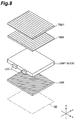
- the backlight device 10 includes a light source 11, a light guide 12, two prism films 13, a reflector film 14, and two diffusing films 15.
- the two prism films 13 are differentiated as a lower prism film 13a and an upper prism film 13b
- the two diffusing films 15 are differentiated as a lower diffusing film 15a and an upper diffusing film 15b.
- the plate-like members with the exception of the light source 11 are stacked in the following order: the reflector film (reflector plate) 14, the light guide 12, the lower diffusing film 15a, the lower prism film 13a, the upper prism film 13b, and the upper diffusing film 15b.
- the light source 11 is disposed so as to be adjacent to a side face of the light guide 12 and, thus, the backlight device 10 is an edge-lit type (side-lit type) device.
- the light source 11 consists of three light emitting diodes (LED), but the number of the light emitting diodes (LED) is not particularly limited. Additionally, the light source 11 may be a different illuminant such as a cold cathode tube, or the like.
- the light source 11 may be disposed on only one side face of the light guide 12, or may be disposed on two opposing side faces of the light guide 12.
- the light guide 12 is a plate-like member for directing light that enters from the light source 11 in a direction normal to the liquid crystal panel 20 (the y-axis direction).
- a cross-sectional shape of the light guide 12 parallel to the y-z plane is rectangular, but a configuration is possible wherein the cross-section is tapered so as to partially or uniformly narrow with distance from the light source 11.
- the lower diffusing film 15a and the upper diffusing film 15b are plate-like members provided for the purpose of eliminating inconsistencies and the like in luminance (brightness) at a front surface of the liquid crystal panel 20.
- Both of the two prism films 13 are plate-like members that are used to increase the luminance at the front surface of the liquid crystal panel 20.
- Examples of products that can be used as the prism films 13 include TBEF (manufactured by 3M).
- a prism-like pattern (hereinafter referred to as the "prism pattern") is formed on a top face (first face) of each of the prism films 13.
- the prism pattern can be configured as a pattern in which a plurality of collapsed triangular poles is arranged in a uniform direction. Additionally, the prism pattern can be configured as a pattern in which mountain-like protrusions formed from two slopes that sandwich a linear ridge line are arranged in a uniform direction. Alternatively, the prism pattern can be configured as a pattern in which "V" shaped grooves extending along a uniform direction are arranged in a uniform direction.
- the ridge lines of the prism patterns of the lower prism film 13a and the upper prism film 13b overlap so as to be perpendicular to each other.
- the reflecting polarization film is a plate-like member that is used to increase the luminance at the front surface of the liquid crystal panel 20.
- Examples of products that can be used as the reflecting polarization film include DBEF (manufactured by 3M).
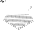
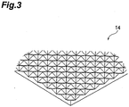
- the reflector film 14 is a plate-like member wherein the top face thereof is a reflection face that totally reflects light. Therefore, the reflection face (indirectly) opposes the bottom face of the prism films 13. Examples of products that can be used as the reflector film 14 include silver reflector plates and ESR (manufactured by 3M). A scattering pattern is formed on the reflection face.
- the scattering pattern may be a prism pattern similar to the prism films 13, and in such a case, a unit component of the scattering pattern is a prism. Additionally, the scattering pattern may be a pattern in which pyramidal protrusions are arranged. In the first embodiment illustrated in FIG. 3 , the unit component of the scattering pattern is a four-sided pyramidal protrusion, but the protrusions may be a different shape such as a three-sided pyramid or the like. Additionally, the scattering pattern may be a pattern in which pyramidal recesses are arranged. In the example illustrated in FIG. 4 , the unit component of the scattering pattern is a four-sided pyramidal recess, but the recesses may be a different shape such as a three-sided pyramid or the like.
- the specific shape of the scattering pattern is not limited.
- at least one of the slopes forming the scattering pattern must be formed while taking into consideration the direction of the slope forming the prism pattern of each of the prism films 13.
- the first normal line axis of the slope forming the prism pattern of each of the prism films 13 and a second normal line axis of one slope forming the scattering pattern are projected on an imaginary plane 30 parallel to the liquid crystal panel 20, the projected two normal line axes must form an acute angle.
- the angle formed by the first normal line axis and the second normal line axis is referred to as the "bias".
- a minimum of the bias (acute angle) may be 5 degrees or 25 degrees.
- a maximum of the bias may be 65 degrees or 85 degrees.
- the liquid crystal panel 20 and each of the plate-like members that form the backlight device 10 are substantially parallel and, therefore, the imaginary plane 30 is a plane that is parallel with each of the plate-like members.
- the scattering pattern is the prism pattern illustrated in the example of FIG. 5
- the acute angle formed by a normal line axis 42 of the scattering pattern of the reflector film 14 and a normal line axis 41 a of the prism pattern of the lower prism film 13a is ⁇ a degrees
- the acute angle formed by the normal line axis 42 and a normal line axis 41b of the prism pattern of the upper prism film 13b is ⁇ b degrees.
- each of the two slopes forming one of the prisms satisfies the relationship that the second normal line axis and the first normal line axis form an acute angle.
- the four slopes forming the four-sided pyramidal protrusions and recesses illustrated in FIGS. 3 and 4 satisfy the relationship that the second normal line axis and the first normal line axis form an acute angle.
- Various forms of the scattering pattern are conceivable, but it is sufficient that at least one of the slopes of the unit components of the scattering pattern satisfy the relationship that the second normal line axis and the first normal line axis form an acute angle.
- the scattering pattern such as that illustrated in FIGS. 2 to 4 can be formed by subjecting the silver reflector plate or the ESR described above to a hot press method or a frame embossing method. Furthermore, after forming the scattering pattern using micro-replication technology, the reflector film (reflector plate) can be obtained by coating a metal such as silver or the like on the front surface of the film (plate) using a sputtering, deposition, or plating method.
- the positional relationship between the slope of the prism pattern on the prism film 13 and the slope of the scattering pattern on the reflector film 14 is set as the first normal line axis (e.g. the normal line axes 41a and 41 b) and the second normal line axis (e.g. the normal line axis 42) projected on the imaginary plane 30 form an acute angle.
- This configuration leads to more of the light that enters from the prism film 13 being reflected at the reflector film 14 in a range where repeated total reflection at the prism film 13 will not occur. At least a portion of the light reflected in this manner transmits through the prism film 13 and travels toward the liquid crystal panel 20. Thus, it is possible to transmit light more efficiently to the liquid crystal panel 20.
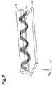
- FIG. 7 illustrates the recycling of light L between the prism films 13 and a reflector plate 90 having a flat reflection face without a scattering pattern.
- the light L travels along the z-axis (along the prism shape of one of the prism films 13) within space enclosed by the plate-like members while repeatedly total reflecting between the prism films 13 and the reflector plate 90.
- the light L appears to come and go between the prism films 13 and the reflector plate 90 substantially along the y-axis. This process continues until the angle of incidence of the light with respect to the prism shape escapes the region of total reflection.
- the phenomenon described above applies likewise for light traveling along the x-axis direction (light traveling while shifting to an adjacent prism).
- the scattering pattern is not simply formed on the reflection face of the reflector film 14, as is the case with the conventional technology.
- the path of light from the prism films 13 to the reflector film 14 is taken into account and a position of the slope of the scattering pattern on the reflector film 14, with respect to the prism pattern on the prism films 13, is determined.
- the slope that is configured as described above changes the direction of reflection of light that enters from the prism films 13.
- the incident light that has a changed direction of reflection escapes to a path different from the path of numerous repeated recycling (see FIG 7 ) and, therefore, a portion of the incident light is refracted at the prism films 13 and is directed toward the liquid crystal panel 20.
- Performance of the backlight device was evaluated via a computer simulation using the software, LightTools® ver. 6.3.0. Attributes of the backlight device model were set as follows.
- FIG. 8 A backlight device model configured as described above and the imaginary plane 30 as described in the embodiment are illustrated in FIG. 8 .
- Three-dimensional coordinates x-axis, y-axis, and z-axis were configured as described in the embodiment.
- FIG. 9 shows the normal lines of the TBEF1 and the TBEF2 and the normal line of the ESR projected on the imaginary plane 30 (x-z plane).
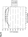
- Cases 1 and 2 Concerning the relationship between the normal lines of the TBEF1, TBEF2, and the ESR, in Cases 1 and 2, the projected normal line of the ESR was parallel to one of the projected normal lines of the TBEF1 and TBEF 2 and, therefore, the bias was 0 degrees (or 90 degrees). In contrast, in Cases 3 to 5, the biases of both the TBEF1 and TBEF 2 were 45 degrees. Thus, Cases 1 and 2 can be considered as Comparative Examples and Cases 3 to 5 can be considered as Working Examples.
- Simulation results are shown in the graph of FIG. 10 .
- the calculated luminance (cd/m 2 ) is shown on the vertical axis and the prism base angle (degrees) of the ESR is shown on the horizontal axis of the graph.
- a backlight device model was configured as in Working Example 1 (see FIG. 8 ). Seven cases were configured where each prism base angle of the ESR, which has an isosceles triangle cross-section, was 10, 15, 20, 25, 30, 35, and 40 degrees, respectively. Then the performance of the backlight was evaluated while varying the bias formed by the ESR and one of the TBEFs (TBEF1 and TBEF2) 5 degrees at a time in a range from 0 to 90 degrees. The point of measurement of the luminance was the same as in Working Example 1.
- Simulation results are shown in the graph of FIG. 11 .
- the calculated luminance (cd/m 2 ) is shown on the vertical axis and the bias (degrees) is shown on the horizontal axis of the graph.
- the backlight device 10 included two prism films 13, but it is possible to use only one prism film. Additionally, in the embodiment, the backlight device 10 included two diffusing films 15, but it is possible only to use one diffusing film or, alternatively, to not use any diffusing films at all.
- the backlight device 10 was described as a component of a liquid crystal display, but the type of display device (display panel) to which the backlight device according to an aspect of the present invention can be applied is not limited to liquid crystal displays (liquid crystal panels).
- the backlight device 10 was an edge-lit device, but an aspect of the present invention can be applied to various types of backlights.
- an aspect of the present invention can be applied to a direct-lit backlight that is not provided with a light guide.
Landscapes
- Physics & Mathematics (AREA)
- General Physics & Mathematics (AREA)
- Optics & Photonics (AREA)
- Nonlinear Science (AREA)
- Mathematical Physics (AREA)
- Chemical & Material Sciences (AREA)
- Crystallography & Structural Chemistry (AREA)
- Planar Illumination Modules (AREA)
- Optical Elements Other Than Lenses (AREA)
- Light Guides In General And Applications Therefor (AREA)
- Liquid Crystal (AREA)
Applications Claiming Priority (2)
| Application Number | Priority Date | Filing Date | Title |
|---|---|---|---|
| JP2011204800 | 2011-09-20 | ||
| PCT/JP2012/074607 WO2013042796A1 (en) | 2011-09-20 | 2012-09-19 | Backlight device |
Publications (2)
| Publication Number | Publication Date |
|---|---|
| EP2758831A1 EP2758831A1 (en) | 2014-07-30 |
| EP2758831B1 true EP2758831B1 (en) | 2017-05-17 |
Family
ID=47003167
Family Applications (1)
| Application Number | Title | Priority Date | Filing Date |
|---|---|---|---|
| EP12769747.2A Not-in-force EP2758831B1 (en) | 2011-09-20 | 2012-09-19 | Backlight device |
Country Status (8)
| Country | Link |
|---|---|
| US (1) | US9423553B2 (pt) |
| EP (1) | EP2758831B1 (pt) |
| JP (1) | JP2014530455A (pt) |
| KR (1) | KR20140066237A (pt) |
| CN (1) | CN103797406B (pt) |
| SG (1) | SG11201400772WA (pt) |
| TW (1) | TW201319645A (pt) |
| WO (1) | WO2013042796A1 (pt) |
Families Citing this family (7)
| Publication number | Priority date | Publication date | Assignee | Title |
|---|---|---|---|---|
| RU2617003C1 (ru) * | 2015-11-05 | 2017-04-19 | Самсунг Электроникс Ко., Лтд. | Световодная пластина и содержащее ее устройство задней подсветки |
| CN107505794B (zh) * | 2017-09-28 | 2020-07-21 | 京东方科技集团股份有限公司 | 一种显示装置及背光源 |
| CN108279526A (zh) * | 2017-12-28 | 2018-07-13 | 重庆市中光电显示技术有限公司 | 侧光式背光模组 |
| TWI657277B (zh) * | 2018-03-06 | 2019-04-21 | 友達光電股份有限公司 | 顯示裝置 |
| CN108679573A (zh) * | 2018-05-31 | 2018-10-19 | 华域视觉科技(上海)有限公司 | Led光源面发光模组及应用其的车灯 |
| JP2023008354A (ja) * | 2021-07-06 | 2023-01-19 | 恵和株式会社 | 光学シート積層体、バックライトユニット、液晶表示装置、情報機器、及びバックライトユニットの製造方法 |
| JP2023008355A (ja) * | 2021-07-06 | 2023-01-19 | 恵和株式会社 | 光学シート積層体、バックライトユニット、液晶表示装置、情報機器、及びバックライトユニットの製造方法 |
Family Cites Families (19)
| Publication number | Priority date | Publication date | Assignee | Title |
|---|---|---|---|---|
| US5359691A (en) * | 1992-10-08 | 1994-10-25 | Briteview Technologies | Backlighting system with a multi-reflection light injection system and using microprisms |
| JPH0794008A (ja) | 1993-09-24 | 1995-04-07 | Chiyatani Sangyo Kk | 面照明装置 |
| JP3682313B2 (ja) * | 1995-03-08 | 2005-08-10 | 日東樹脂工業株式会社 | 面光源装置及び液晶ディスプレイ |
| JP2000214460A (ja) | 1999-01-25 | 2000-08-04 | Sharp Corp | バックライト装置 |
| JP2002124116A (ja) | 2000-08-08 | 2002-04-26 | Yuka Denshi Co Ltd | 面光源装置及びこれを用いた液晶ディスプレイ装置 |
| JP3871913B2 (ja) * | 2000-11-14 | 2007-01-24 | シャープ株式会社 | 反射型表示装置およびプリズムアレイシート |
| KR100638658B1 (ko) | 2004-10-20 | 2006-10-30 | 삼성전기주식회사 | 백라이트 장치 |
| JP2006120975A (ja) | 2004-10-25 | 2006-05-11 | Matsushita Electric Ind Co Ltd | 電子部品装着装置および保持ツール |
| CN101018977B (zh) * | 2005-03-01 | 2010-05-19 | 夏普株式会社 | 背光单元和液晶显示装置 |
| US20090290098A1 (en) * | 2005-06-13 | 2009-11-26 | Tsujiden Co., Ltd. | Reflection sheet for backlight of liquid crystal display device, and backlight of liquid crystal display device using the reflection sheet |
| JP2007115451A (ja) * | 2005-10-18 | 2007-05-10 | Omron Corp | 面光源装置 |
| KR20070077285A (ko) * | 2006-01-23 | 2007-07-26 | 삼성전자주식회사 | 백라이트 어셈블리 및 이를 갖는 표시장치 |
| CN101008683A (zh) * | 2006-01-25 | 2007-08-01 | 扬明光学股份有限公司 | 增光片与背光模组 |
| JP2007220447A (ja) | 2006-02-16 | 2007-08-30 | Harison Toshiba Lighting Corp | サイドライト型バックライト装置 |
| JP4853784B2 (ja) | 2007-01-12 | 2012-01-11 | ミネベア株式会社 | 面状照明装置 |
| KR20100037104A (ko) * | 2007-06-22 | 2010-04-08 | 쓰리엠 이노베이티브 프로퍼티즈 컴파니 | 백라이트 출력 특성을 제어하는 시스템 및 방법 |
| US8721153B2 (en) * | 2007-12-20 | 2014-05-13 | 3M Innovative Properties Company | Backlight reflectors having a prismatic structure |
| CN102227587A (zh) * | 2008-11-27 | 2011-10-26 | 夏普株式会社 | 面光源装置 |
| JP2010262813A (ja) * | 2009-05-01 | 2010-11-18 | Hitachi Displays Ltd | 照明装置及び液晶表示装置 |
-
2012
- 2012-09-19 JP JP2014530432A patent/JP2014530455A/ja active Pending
- 2012-09-19 SG SG11201400772WA patent/SG11201400772WA/en unknown
- 2012-09-19 WO PCT/JP2012/074607 patent/WO2013042796A1/en active Application Filing
- 2012-09-19 US US14/346,233 patent/US9423553B2/en not_active Expired - Fee Related
- 2012-09-19 KR KR1020147010093A patent/KR20140066237A/ko not_active Application Discontinuation
- 2012-09-19 EP EP12769747.2A patent/EP2758831B1/en not_active Not-in-force
- 2012-09-19 CN CN201280045252.5A patent/CN103797406B/zh not_active Expired - Fee Related
- 2012-09-20 TW TW101134533A patent/TW201319645A/zh unknown
Also Published As
| Publication number | Publication date |
|---|---|
| JP2014530455A (ja) | 2014-11-17 |
| TW201319645A (zh) | 2013-05-16 |
| US20150177444A1 (en) | 2015-06-25 |
| US9423553B2 (en) | 2016-08-23 |
| CN103797406B (zh) | 2016-08-17 |
| SG11201400772WA (en) | 2014-04-28 |
| EP2758831A1 (en) | 2014-07-30 |
| KR20140066237A (ko) | 2014-05-30 |
| CN103797406A (zh) | 2014-05-14 |
| WO2013042796A1 (en) | 2013-03-28 |
Similar Documents
| Publication | Publication Date | Title |
|---|---|---|
| EP2758831B1 (en) | Backlight device | |
| JP4168179B2 (ja) | 種々の高さの構造化面を有する光指向性フィルム及び該フィルムから作製された光指向性製品 | |
| US8717676B2 (en) | Light outcoupling structure for a lighting device | |
| JP5193987B2 (ja) | 導光板及びバックライトモジュール | |
| US8915635B2 (en) | Backlight having dual collimating reflectors | |
| KR100898100B1 (ko) | 프리즘 시트 | |
| KR100978078B1 (ko) | 프리즘 시트와 이를 구비한 액정표시장치 | |
| US20130286679A1 (en) | Light guide plate and backlight module using the same | |
| US8287172B2 (en) | Planar illumination device | |
| CN101095077A (zh) | 具有带凹入的棱锥形结构的结构化表面的光学薄膜 | |
| JP5199830B2 (ja) | 表示装置 | |
| US7656597B2 (en) | Prism sheet and backlight module using the same | |
| JP5071675B2 (ja) | 照明装置および表示装置 | |
| JP2014515499A (ja) | 裸眼立体ディスプレイ用の微細複製フィルム | |
| JPWO2007066729A1 (ja) | 面発光装置及び液晶表示装置 | |
| US7753543B2 (en) | Prism sheet and backlight module using the same | |
| CN101191845A (zh) | 光学板 | |
| JP2013016472A (ja) | 導光板 | |
| CN102588835A (zh) | 一种用于液晶显示器的新型背光模组 | |
| CN101363926B (zh) | 液晶显示装置及其棱镜片 | |
| CN1580901A (zh) | 背光模组及其导光板 | |
| WO2007046625A1 (en) | Light guide plate | |
| CN101191852A (zh) | 光学板 | |
| CN101196574A (zh) | 光学板 | |
| JP3215902U (ja) | 光学フィルム及び表示装置 |
Legal Events
| Date | Code | Title | Description |
|---|---|---|---|
| PUAI | Public reference made under article 153(3) epc to a published international application that has entered the european phase |
Free format text: ORIGINAL CODE: 0009012 |
|
| 17P | Request for examination filed |
Effective date: 20140325 |
|
| AK | Designated contracting states |
Kind code of ref document: A1 Designated state(s): AL AT BE BG CH CY CZ DE DK EE ES FI FR GB GR HR HU IE IS IT LI LT LU LV MC MK MT NL NO PL PT RO RS SE SI SK SM TR |
|
| DAX | Request for extension of the european patent (deleted) | ||
| GRAP | Despatch of communication of intention to grant a patent |
Free format text: ORIGINAL CODE: EPIDOSNIGR1 |
|
| STAA | Information on the status of an ep patent application or granted ep patent |
Free format text: STATUS: GRANT OF PATENT IS INTENDED |
|
| INTG | Intention to grant announced |
Effective date: 20161124 |
|
| GRAS | Grant fee paid |
Free format text: ORIGINAL CODE: EPIDOSNIGR3 |
|
| GRAA | (expected) grant |
Free format text: ORIGINAL CODE: 0009210 |
|
| STAA | Information on the status of an ep patent application or granted ep patent |
Free format text: STATUS: THE PATENT HAS BEEN GRANTED |
|
| AK | Designated contracting states |
Kind code of ref document: B1 Designated state(s): AL AT BE BG CH CY CZ DE DK EE ES FI FR GB GR HR HU IE IS IT LI LT LU LV MC MK MT NL NO PL PT RO RS SE SI SK SM TR |
|
| REG | Reference to a national code |
Ref country code: GB Ref legal event code: FG4D |
|
| REG | Reference to a national code |
Ref country code: CH Ref legal event code: EP |
|
| REG | Reference to a national code |
Ref country code: IE Ref legal event code: FG4D |
|
| REG | Reference to a national code |
Ref country code: AT Ref legal event code: REF Ref document number: 894990 Country of ref document: AT Kind code of ref document: T Effective date: 20170615 |
|
| REG | Reference to a national code |
Ref country code: DE Ref legal event code: R096 Ref document number: 602012032587 Country of ref document: DE |
|
| REG | Reference to a national code |
Ref country code: NL Ref legal event code: MP Effective date: 20170517 |
|
| REG | Reference to a national code |
Ref country code: LT Ref legal event code: MG4D |
|
| REG | Reference to a national code |
Ref country code: AT Ref legal event code: MK05 Ref document number: 894990 Country of ref document: AT Kind code of ref document: T Effective date: 20170517 |
|
| PG25 | Lapsed in a contracting state [announced via postgrant information from national office to epo] |
Ref country code: GR Free format text: LAPSE BECAUSE OF FAILURE TO SUBMIT A TRANSLATION OF THE DESCRIPTION OR TO PAY THE FEE WITHIN THE PRESCRIBED TIME-LIMIT Effective date: 20170818 Ref country code: NO Free format text: LAPSE BECAUSE OF FAILURE TO SUBMIT A TRANSLATION OF THE DESCRIPTION OR TO PAY THE FEE WITHIN THE PRESCRIBED TIME-LIMIT Effective date: 20170817 Ref country code: LT Free format text: LAPSE BECAUSE OF FAILURE TO SUBMIT A TRANSLATION OF THE DESCRIPTION OR TO PAY THE FEE WITHIN THE PRESCRIBED TIME-LIMIT Effective date: 20170517 Ref country code: HR Free format text: LAPSE BECAUSE OF FAILURE TO SUBMIT A TRANSLATION OF THE DESCRIPTION OR TO PAY THE FEE WITHIN THE PRESCRIBED TIME-LIMIT Effective date: 20170517 Ref country code: FI Free format text: LAPSE BECAUSE OF FAILURE TO SUBMIT A TRANSLATION OF THE DESCRIPTION OR TO PAY THE FEE WITHIN THE PRESCRIBED TIME-LIMIT Effective date: 20170517 Ref country code: ES Free format text: LAPSE BECAUSE OF FAILURE TO SUBMIT A TRANSLATION OF THE DESCRIPTION OR TO PAY THE FEE WITHIN THE PRESCRIBED TIME-LIMIT Effective date: 20170517 Ref country code: AT Free format text: LAPSE BECAUSE OF FAILURE TO SUBMIT A TRANSLATION OF THE DESCRIPTION OR TO PAY THE FEE WITHIN THE PRESCRIBED TIME-LIMIT Effective date: 20170517 |
|
| PG25 | Lapsed in a contracting state [announced via postgrant information from national office to epo] |
Ref country code: PL Free format text: LAPSE BECAUSE OF FAILURE TO SUBMIT A TRANSLATION OF THE DESCRIPTION OR TO PAY THE FEE WITHIN THE PRESCRIBED TIME-LIMIT Effective date: 20170517 Ref country code: NL Free format text: LAPSE BECAUSE OF FAILURE TO SUBMIT A TRANSLATION OF THE DESCRIPTION OR TO PAY THE FEE WITHIN THE PRESCRIBED TIME-LIMIT Effective date: 20170517 Ref country code: IS Free format text: LAPSE BECAUSE OF FAILURE TO SUBMIT A TRANSLATION OF THE DESCRIPTION OR TO PAY THE FEE WITHIN THE PRESCRIBED TIME-LIMIT Effective date: 20170917 Ref country code: BG Free format text: LAPSE BECAUSE OF FAILURE TO SUBMIT A TRANSLATION OF THE DESCRIPTION OR TO PAY THE FEE WITHIN THE PRESCRIBED TIME-LIMIT Effective date: 20170817 Ref country code: SE Free format text: LAPSE BECAUSE OF FAILURE TO SUBMIT A TRANSLATION OF THE DESCRIPTION OR TO PAY THE FEE WITHIN THE PRESCRIBED TIME-LIMIT Effective date: 20170517 Ref country code: RS Free format text: LAPSE BECAUSE OF FAILURE TO SUBMIT A TRANSLATION OF THE DESCRIPTION OR TO PAY THE FEE WITHIN THE PRESCRIBED TIME-LIMIT Effective date: 20170517 Ref country code: LV Free format text: LAPSE BECAUSE OF FAILURE TO SUBMIT A TRANSLATION OF THE DESCRIPTION OR TO PAY THE FEE WITHIN THE PRESCRIBED TIME-LIMIT Effective date: 20170517 |
|
| PG25 | Lapsed in a contracting state [announced via postgrant information from national office to epo] |
Ref country code: RO Free format text: LAPSE BECAUSE OF FAILURE TO SUBMIT A TRANSLATION OF THE DESCRIPTION OR TO PAY THE FEE WITHIN THE PRESCRIBED TIME-LIMIT Effective date: 20170517 Ref country code: EE Free format text: LAPSE BECAUSE OF FAILURE TO SUBMIT A TRANSLATION OF THE DESCRIPTION OR TO PAY THE FEE WITHIN THE PRESCRIBED TIME-LIMIT Effective date: 20170517 Ref country code: SK Free format text: LAPSE BECAUSE OF FAILURE TO SUBMIT A TRANSLATION OF THE DESCRIPTION OR TO PAY THE FEE WITHIN THE PRESCRIBED TIME-LIMIT Effective date: 20170517 Ref country code: CZ Free format text: LAPSE BECAUSE OF FAILURE TO SUBMIT A TRANSLATION OF THE DESCRIPTION OR TO PAY THE FEE WITHIN THE PRESCRIBED TIME-LIMIT Effective date: 20170517 Ref country code: DK Free format text: LAPSE BECAUSE OF FAILURE TO SUBMIT A TRANSLATION OF THE DESCRIPTION OR TO PAY THE FEE WITHIN THE PRESCRIBED TIME-LIMIT Effective date: 20170517 |
|
| REG | Reference to a national code |
Ref country code: DE Ref legal event code: R097 Ref document number: 602012032587 Country of ref document: DE |
|
| PG25 | Lapsed in a contracting state [announced via postgrant information from national office to epo] |
Ref country code: IT Free format text: LAPSE BECAUSE OF FAILURE TO SUBMIT A TRANSLATION OF THE DESCRIPTION OR TO PAY THE FEE WITHIN THE PRESCRIBED TIME-LIMIT Effective date: 20170517 Ref country code: SM Free format text: LAPSE BECAUSE OF FAILURE TO SUBMIT A TRANSLATION OF THE DESCRIPTION OR TO PAY THE FEE WITHIN THE PRESCRIBED TIME-LIMIT Effective date: 20170517 |
|
| PLBE | No opposition filed within time limit |
Free format text: ORIGINAL CODE: 0009261 |
|
| STAA | Information on the status of an ep patent application or granted ep patent |
Free format text: STATUS: NO OPPOSITION FILED WITHIN TIME LIMIT |
|
| REG | Reference to a national code |
Ref country code: DE Ref legal event code: R119 Ref document number: 602012032587 Country of ref document: DE |
|
| 26N | No opposition filed |
Effective date: 20180220 |
|
| REG | Reference to a national code |
Ref country code: CH Ref legal event code: PL |
|
| GBPC | Gb: european patent ceased through non-payment of renewal fee |
Effective date: 20170919 |
|
| PG25 | Lapsed in a contracting state [announced via postgrant information from national office to epo] |
Ref country code: SI Free format text: LAPSE BECAUSE OF FAILURE TO SUBMIT A TRANSLATION OF THE DESCRIPTION OR TO PAY THE FEE WITHIN THE PRESCRIBED TIME-LIMIT Effective date: 20170517 Ref country code: MC Free format text: LAPSE BECAUSE OF FAILURE TO SUBMIT A TRANSLATION OF THE DESCRIPTION OR TO PAY THE FEE WITHIN THE PRESCRIBED TIME-LIMIT Effective date: 20170517 |
|
| REG | Reference to a national code |
Ref country code: IE Ref legal event code: MM4A |
|
| REG | Reference to a national code |
Ref country code: BE Ref legal event code: MM Effective date: 20170930 |
|
| PG25 | Lapsed in a contracting state [announced via postgrant information from national office to epo] |
Ref country code: LU Free format text: LAPSE BECAUSE OF NON-PAYMENT OF DUE FEES Effective date: 20170919 |
|
| REG | Reference to a national code |
Ref country code: FR Ref legal event code: ST Effective date: 20180531 |
|
| PG25 | Lapsed in a contracting state [announced via postgrant information from national office to epo] |
Ref country code: LI Free format text: LAPSE BECAUSE OF NON-PAYMENT OF DUE FEES Effective date: 20170930 Ref country code: IE Free format text: LAPSE BECAUSE OF NON-PAYMENT OF DUE FEES Effective date: 20170919 Ref country code: CH Free format text: LAPSE BECAUSE OF NON-PAYMENT OF DUE FEES Effective date: 20170930 Ref country code: GB Free format text: LAPSE BECAUSE OF NON-PAYMENT OF DUE FEES Effective date: 20170919 Ref country code: DE Free format text: LAPSE BECAUSE OF NON-PAYMENT OF DUE FEES Effective date: 20180404 |
|
| PG25 | Lapsed in a contracting state [announced via postgrant information from national office to epo] |
Ref country code: BE Free format text: LAPSE BECAUSE OF NON-PAYMENT OF DUE FEES Effective date: 20170930 Ref country code: FR Free format text: LAPSE BECAUSE OF NON-PAYMENT OF DUE FEES Effective date: 20171002 |
|
| PG25 | Lapsed in a contracting state [announced via postgrant information from national office to epo] |
Ref country code: MT Free format text: LAPSE BECAUSE OF NON-PAYMENT OF DUE FEES Effective date: 20170919 |
|
| PG25 | Lapsed in a contracting state [announced via postgrant information from national office to epo] |
Ref country code: HU Free format text: LAPSE BECAUSE OF FAILURE TO SUBMIT A TRANSLATION OF THE DESCRIPTION OR TO PAY THE FEE WITHIN THE PRESCRIBED TIME-LIMIT; INVALID AB INITIO Effective date: 20120919 |
|
| PG25 | Lapsed in a contracting state [announced via postgrant information from national office to epo] |
Ref country code: CY Free format text: LAPSE BECAUSE OF NON-PAYMENT OF DUE FEES Effective date: 20170517 |
|
| PG25 | Lapsed in a contracting state [announced via postgrant information from national office to epo] |
Ref country code: MK Free format text: LAPSE BECAUSE OF FAILURE TO SUBMIT A TRANSLATION OF THE DESCRIPTION OR TO PAY THE FEE WITHIN THE PRESCRIBED TIME-LIMIT Effective date: 20170517 |
|
| PG25 | Lapsed in a contracting state [announced via postgrant information from national office to epo] |
Ref country code: TR Free format text: LAPSE BECAUSE OF FAILURE TO SUBMIT A TRANSLATION OF THE DESCRIPTION OR TO PAY THE FEE WITHIN THE PRESCRIBED TIME-LIMIT Effective date: 20170517 |
|
| PG25 | Lapsed in a contracting state [announced via postgrant information from national office to epo] |
Ref country code: PT Free format text: LAPSE BECAUSE OF FAILURE TO SUBMIT A TRANSLATION OF THE DESCRIPTION OR TO PAY THE FEE WITHIN THE PRESCRIBED TIME-LIMIT Effective date: 20170517 |
|
| PG25 | Lapsed in a contracting state [announced via postgrant information from national office to epo] |
Ref country code: AL Free format text: LAPSE BECAUSE OF FAILURE TO SUBMIT A TRANSLATION OF THE DESCRIPTION OR TO PAY THE FEE WITHIN THE PRESCRIBED TIME-LIMIT Effective date: 20170517 |