EP2757403A1 - Vibrating mirror device and electronic device having a projector function - Google Patents
Vibrating mirror device and electronic device having a projector function Download PDFInfo
- Publication number
- EP2757403A1 EP2757403A1 EP13196953.7A EP13196953A EP2757403A1 EP 2757403 A1 EP2757403 A1 EP 2757403A1 EP 13196953 A EP13196953 A EP 13196953A EP 2757403 A1 EP2757403 A1 EP 2757403A1
- Authority
- EP
- European Patent Office
- Prior art keywords
- driving
- insulating layer
- detecting electrode
- top face
- driving portion
- Prior art date
- Legal status (The legal status is an assumption and is not a legal conclusion. Google has not performed a legal analysis and makes no representation as to the accuracy of the status listed.)
- Withdrawn
Links
- 239000011347 resin Substances 0.000 claims description 8
- 229920005989 resin Polymers 0.000 claims description 8
- 239000013078 crystal Substances 0.000 description 88
- 238000001514 detection method Methods 0.000 description 7
- 229910001020 Au alloy Inorganic materials 0.000 description 6
- 238000009792 diffusion process Methods 0.000 description 6
- 230000000694 effects Effects 0.000 description 6
- 229910052451 lead zirconate titanate Inorganic materials 0.000 description 5
- 239000007769 metal material Substances 0.000 description 4
- 230000003287 optical effect Effects 0.000 description 4
- 229920001721 polyimide Polymers 0.000 description 4
- 239000009719 polyimide resin Substances 0.000 description 4
- 239000000758 substrate Substances 0.000 description 4
- 238000005452 bending Methods 0.000 description 3
- 239000011248 coating agent Substances 0.000 description 2
- 238000000576 coating method Methods 0.000 description 2
- 229910052802 copper Inorganic materials 0.000 description 2
- HFGPZNIAWCZYJU-UHFFFAOYSA-N lead zirconate titanate Chemical compound [O-2].[O-2].[O-2].[O-2].[O-2].[Ti+4].[Zr+4].[Pb+2] HFGPZNIAWCZYJU-UHFFFAOYSA-N 0.000 description 2
- 239000000463 material Substances 0.000 description 2
- 230000002093 peripheral effect Effects 0.000 description 2
- 229910052719 titanium Inorganic materials 0.000 description 2
- 239000010936 titanium Substances 0.000 description 2
- 229910052726 zirconium Inorganic materials 0.000 description 2
- 229910003334 KNbO3 Inorganic materials 0.000 description 1
- RTAQQCXQSZGOHL-UHFFFAOYSA-N Titanium Chemical compound [Ti] RTAQQCXQSZGOHL-UHFFFAOYSA-N 0.000 description 1
- XLOMVQKBTHCTTD-UHFFFAOYSA-N Zinc monoxide Chemical compound [Zn]=O XLOMVQKBTHCTTD-UHFFFAOYSA-N 0.000 description 1
- QCWXUUIWCKQGHC-UHFFFAOYSA-N Zirconium Chemical compound [Zr] QCWXUUIWCKQGHC-UHFFFAOYSA-N 0.000 description 1
- PQCCZSBUXOQGIU-UHFFFAOYSA-N [La].[Pb] Chemical compound [La].[Pb] PQCCZSBUXOQGIU-UHFFFAOYSA-N 0.000 description 1
- 230000008602 contraction Effects 0.000 description 1
- 238000010586 diagram Methods 0.000 description 1
- 239000003989 dielectric material Substances 0.000 description 1
- 238000007599 discharging Methods 0.000 description 1
- 238000006073 displacement reaction Methods 0.000 description 1
- 238000005516 engineering process Methods 0.000 description 1
- 229910052746 lanthanum Inorganic materials 0.000 description 1
- 229910052745 lead Inorganic materials 0.000 description 1
- 238000000034 method Methods 0.000 description 1
- 238000012986 modification Methods 0.000 description 1
- 230000004048 modification Effects 0.000 description 1
- 238000000059 patterning Methods 0.000 description 1
- 238000000206 photolithography Methods 0.000 description 1
- UKDIAJWKFXFVFG-UHFFFAOYSA-N potassium;oxido(dioxo)niobium Chemical compound [K+].[O-][Nb](=O)=O UKDIAJWKFXFVFG-UHFFFAOYSA-N 0.000 description 1
- 230000002250 progressing effect Effects 0.000 description 1
- UYLYBEXRJGPQSH-UHFFFAOYSA-N sodium;oxido(dioxo)niobium Chemical compound [Na+].[O-][Nb](=O)=O UYLYBEXRJGPQSH-UHFFFAOYSA-N 0.000 description 1
- 238000004528 spin coating Methods 0.000 description 1
- 238000004544 sputter deposition Methods 0.000 description 1
- 239000010935 stainless steel Substances 0.000 description 1
- 229910001220 stainless steel Inorganic materials 0.000 description 1
- 229920002803 thermoplastic polyurethane Polymers 0.000 description 1
Images




Classifications
-
- G—PHYSICS
- G02—OPTICS
- G02B—OPTICAL ELEMENTS, SYSTEMS OR APPARATUS
- G02B26/00—Optical devices or arrangements for the control of light using movable or deformable optical elements
- G02B26/08—Optical devices or arrangements for the control of light using movable or deformable optical elements for controlling the direction of light
- G02B26/10—Scanning systems
- G02B26/101—Scanning systems with both horizontal and vertical deflecting means, e.g. raster or XY scanners
-
- G—PHYSICS
- G02—OPTICS
- G02B—OPTICAL ELEMENTS, SYSTEMS OR APPARATUS
- G02B26/00—Optical devices or arrangements for the control of light using movable or deformable optical elements
- G02B26/08—Optical devices or arrangements for the control of light using movable or deformable optical elements for controlling the direction of light
- G02B26/0816—Optical devices or arrangements for the control of light using movable or deformable optical elements for controlling the direction of light by means of one or more reflecting elements
- G02B26/0833—Optical devices or arrangements for the control of light using movable or deformable optical elements for controlling the direction of light by means of one or more reflecting elements the reflecting element being a micromechanical device, e.g. a MEMS mirror, DMD
- G02B26/0858—Optical devices or arrangements for the control of light using movable or deformable optical elements for controlling the direction of light by means of one or more reflecting elements the reflecting element being a micromechanical device, e.g. a MEMS mirror, DMD the reflecting means being moved or deformed by piezoelectric means
-
- H—ELECTRICITY
- H04—ELECTRIC COMMUNICATION TECHNIQUE
- H04N—PICTORIAL COMMUNICATION, e.g. TELEVISION
- H04N9/00—Details of colour television systems
- H04N9/12—Picture reproducers
- H04N9/31—Projection devices for colour picture display, e.g. using electronic spatial light modulators [ESLM]
- H04N9/3129—Projection devices for colour picture display, e.g. using electronic spatial light modulators [ESLM] scanning a light beam on the display screen
- H04N9/3135—Driving therefor
Definitions
- the present invention relates generally to a vibrating mirror device and an electronic device having a projector function, e.g., a vibrating element and an electronic device having a projector function that is provided with a driving portion that includes a detecting electrode for detecting an amount of deformation in a piezoelectric element (e.g., crystal).
- a piezoelectric element e.g., crystal
- Conventional vibrating mirror devices are provided with driving portions that include detecting electrodes for detecting an amount of deformation of a piezoelectric crystal (referencing, for example, Patent Citation 1).
- Patent Citation 1 discloses a single-axis optical scanner (vibrating mirror device) comprising an essentially circular mirror portion and a cantilever (a bar that is held on one end) elastic portion wherein the free end is connected to the mirror portion and the stationary end is connected to a stationary frame.
- a piezoelectric crystal is formed in a state where it is held between a top electrode and a bottom electrode in a specific location of the elastic portion.
- the structure is such that a single piezoelectric crystal is provided with two sets of top electrodes and bottom electrodes, where the piezoelectric crystal is driven by applying a voltage between the top electrode and the bottom electrode on one side, and the potential difference between the electrodes accompanying deformation of the piezoelectric crystal is detected using the top electrode and the bottom electrode on the other side.
- the structure is such that the top electrodes and bottom electrodes extend from the elastic portion to a stationary frame at some distance, where the external interconnections for the power supply and the interconnections from a displacement detecting circuit are respectively wire-bonded to the top electrodes and the bottom electrodes at a part of the stationary frame.
- Patent Document 1 Japanese Unexamined Patent Application Publication 2009-163154
- the structure is intended to cause a mirror portion to reciprocate around a single axis, thus making it possible to connect the interconnections from the dislocation detecting circuit and the like to the top electrode and the bottom electrode at the stationary frame part.
- the detecting electrodes for detecting the amount of deformation (the potential difference) for the driving portion for the first axis
- the detecting electrodes it is necessary for the detecting electrodes to lead out to a stationary frame that is to the outside of not only the driving portion for the first axis but also the driving portion for the second axis (the driving portion for the first axis causes the mirror portion to reciprocate around the first axis, and the driving portion for the second axis causes the mirror portion to reciprocate around the second axis).
- the interconnections for leading out from the detecting electrodes are formed in the same layer as the detecting electrodes for the piezoelectric crystal, through patterning or the like, to lead out to the outside.
- the surface charge charged at the part where the detecting electrode accompanying deformation of the piezoelectric crystal is affected by the piezoelectric crystal so as to discharge (diffuse) into the lead interconnections. Because of this, even if a surface charge is produced in the detecting electrode in an amount in accordance with the deformation of the piezoelectric crystal, a voltage value (a potential difference) will be detected by the detecting electrode in a state wherein a voltage drop was caused by the surface charge discharging into the lead interconnections. Moreover, because the detecting electrode will actually detect a voltage value smaller than the voltage value of that should be detected, accurate detection of the amount of deformation of the piezoelectric crystal is difficult.
- One or more embodiments of the present invention provide a vibrating mirror device able to suppress deformation of the mirror portion, and an electronic device having a projector function, provided with the vibrating mirror device.
- one or more embodiments of the present invention provide a vibrating mirror device and an electronic device having a projector function so as to prevent a voltage value from being detected by the detecting electrodes in a state wherein there has been a voltage drop caused by the discharge of the surface charge.
- a vibrating mirror device may comprise a mirror portion, a driving portion including a detecting electrode configured to detect an amount of deformation of a piezoelectric element when driving the mirror portion by applying a voltage to cause the piezoelectric element to deform, an insulating layer, and a first lead interconnection.
- the mirror portion may comprise a mirror.
- the driving portion may comprise a driving circuit.
- the insulating layer may be formed on a top face of the piezoelectric element.
- the first lead interconnection is formed on the top face of the insulating layer.
- the first lead interconnection is configured to contact the detecting electrode.
- the first lead interconnection extends to a region outside of the driving portion.
- the insulating layer (which may be formed on the top face of the piezoelectric element) and the first lead interconnection (which may be formed on the top face of the insulating layer, may be connected to the detecting electrode, and may extend to a region outside of the driving portion) of the vibrating mirror device make it possible to lead out, to a region on the outside of the driving portion, the first lead interconnection connected to the detecting electrode along the top face of the insulating layer (which may be separated from the piezoelectric element, e.g., crystal) without contacting the top face of the piezoelectric element on which the detecting electrode is formed.
- the amount of deformation of the piezoelectric element (the voltage value produced through the piezoelectric effect) may be detected through the detecting electrode in a state wherein only the detecting electrode portion is in contact with the top face of the piezoelectric element, regardless of the length of the first lead interconnection.
- the first lead interconnection may be separated from the piezoelectric element by the insulating layer, so as to prevent the discharge (diffusion) of the surface charge produced at the part at the detecting electrode into the first lead interconnection, affected by the piezoelectric element disposed on the bottom layer side of the first lead interconnection as well.
- the detecting electrode it is possible to prevent detection, by the detecting electrode, of a voltage value in a state wherein there has been a voltage drop caused by the discharge of the surface charge. Moreover, in one or more embodiments, because the voltage value detected at the detecting electrode part may be detected in a state wherein there is no voltage drop, it is possible to detect with good accuracy the amount of deformation of the piezoelectric element (the driving portion).
- the insulating layer may be formed so as to cover the detecting electrode on the top face of the piezoelectric element.
- the first lead interconnection may be connected to the detecting electrode through a hole portion that passes through the insulating layer, in a thickness direction, at a part that corresponds to the detecting electrode. Structuring in this way may enable easy connection of the first lead interconnection, which may be formed on the top face of the insulating layer and may extend along the top face of the insulating layer, to a detecting electrode positioned on a layer below the insulating layer through a hole portion that passes through the insulating layer in the direction of thickness.
- the driving portion may be structured so as to undergo flexural deformation when driven.
- the insulating layer may be made from a resin capable of undergoing flexural deformation. With such a structure, the insulating layer formed from a resin that can undergo flexural deformation may be formed on the top face of the piezoelectric element, making it possible to prevent the insulating layer from resisting the deformation of the driving portion even when a driving portion that includes a piezoelectric element undergoes bending deformation (flexural deformation).
- the driving portion may further include a driving electrode, which may be formed so as to contact the top face of the piezoelectric element, for applying a voltage to cause the piezoelectric element to undergo flexural deformation to drive the mirror portion.
- the vibrating mirror device may further include a second lead interconnection. The second lead interconnection may be formed on the top face of the insulating layer, may be connected to the driving electrode of the driving portion, and may extend to a region outside of the driving portion.
- the second lead interconnection connected to the driving electrode can also lead out, to a region outside of the driving portion, by extending over the top face of the insulating layer, separated from the piezoelectric element, without contacting the top face of the piezoelectric element whereon the driving electrode is formed. That is, in addition to the first lead interconnection, a second lead interconnection may lead out similarly to an outer region that is further than the driving portion, so as to eliminate the need to perform wire bonding of the lead lines (outer interconnections) at a location in the vicinity of the driving portion. Consequently, this makes it possible, for example, to avoid reliably damage to the driving portion that is caused by the wire bonding.
- the insulating layer may be formed so as to cover a region of a portion that includes the detecting electrode on the top face of the piezoelectric element.
- the insulating layer may be formed on only that part of the entire surface (top face) of the piezoelectric element whereon the detecting electrode is formed, so that, to that extent, the stress of the insulating layer does not greatly affect the flexural deformation of the piezoelectric element. This makes it possible, for example, to prevent effectively reduction in the deformation force of the piezoelectric element that would be caused by stress in the insulating layer.
- the detecting electrode may have a long thin shape that extends in a first direction.
- an interconnection length of the first lead interconnection may be greater than a length of the lengthwise direction of the detecting electrode.
- the first lead interconnection may extend along the top face of the insulating layer, which is separated from the piezoelectric element, thus making it possible to prevent the discharge of the surface charge (produced at that part of the detecting electrode) to the first lead interconnection, which has a long interconnection length (a large interconnection surface area).
- the driving portion may include a first driving portion for causing the mirror portion to reciprocate around a first axis, and a second driving portion for causing the mirror portion to reciprocate around a second axis that is substantially perpendicular to the first axis.
- the insulating layer may be formed on the top face of the piezoelectric element across the first driving portion and the second driving portion.
- the first lead interconnection may lead out from the detecting electrode of the first driving portion and is routed sequentially over a top face of the insulating layer corresponding to the first driving portion and a top face of the insulating layer corresponding to the second driving portion, so as to lead out to a region outside of the second driving portion.
- an insulating layer may be interposed between the first lead interconnection and the piezoelectric element of the second driving portion as well, in the same manner as with the first driving portion part, thus making it possible to prevent the discharge (diffusion) of the surface charge that is produced at the detecting electrode part of the first driving portion into the first lead interconnection, affected by the piezoelectric element of the second driving portion.
- an electronic device having a projector function may comprise: a laser beam producing portion configured to produce a laser beam; a controlling portion configured to analyze an inputted video to recognize pixel information; and a vibrating mirror device configured to scan the laser beam.
- the vibrating mirror device may be as described in any of the above-mentioned embodiments.
- the vibrating mirror device may include: a mirror portion; a driving portion including a detecting electrode configured to detect an amount of deformation of a piezoelectric element when driving the mirror portion by applying a voltage to cause the piezoelectric element to deform; an insulating layer formed on a top face of the piezoelectric element; and a lead interconnection formed on the top face of the insulating layer and extending to a region outside of the driving portion, the first lead interconnection being configured to contact the detecting electrode of the driving portion.
- the electronic device having the projector function may comprise a vibrating mirror device which may include an insulating layer formed on the top face of the piezoelectric element and the first lead interconnection (which may be formed on the top face of the insulating layer, connected to the detecting electrode, and extend to a region that is outside of the driving portion), which makes it possible to lead out, to a region on the outside of the driving portion, the lead interconnection connected to the detecting electrode along the top face of the insulating layer (which may be separated from the piezoelectric element) without contacting the top face of the piezoelectric element on which the detecting electrode is formed.
- a vibrating mirror device which may include an insulating layer formed on the top face of the piezoelectric element and the first lead interconnection (which may be formed on the top face of the insulating layer, connected to the detecting electrode, and extend to a region that is outside of the driving portion), which makes it possible to lead out, to a region on the outside of the driving portion, the lead interconnection connected to the detecting
- the amount of deformation of the piezoelectric element (the voltage value that is produced through the piezoelectric effect) may be detected through the detecting electrode in a state wherein only the detecting electrode portion is in contact with the top face of the piezoelectric element, regardless of the length of the lead interconnection.
- the lead interconnection may be separated from the piezoelectric element by the insulating layer so as to prevent the discharge (diffusion) of the surface charge produced at the part at the detecting electrode into the lead interconnection, affected by the piezoelectric element disposed on the bottom layer side of the lead interconnection as well.
- the vibrating mirror device it is possible to prevent the detection, by the detecting electrode, of a voltage value in a state wherein there has been a voltage drop caused by the discharge of the surface charge. Moreover, because the voltage value detected at the detecting electrode part is detected in a state wherein there is no voltage drop, it is possible to detect with good accuracy the amount of deformation of the piezoelectric element (the driving portion). Consequently, the driving of the vibrating mirror device may be controlled in a state wherein the amount of deformation of the piezoelectric element is detected accurately, so that in the electronic device with the projector function, the laser beam can project an image in a state wherein the scanning is accurate.
- one or more embodiments of the present invention make it possible to prevent the detection, by the detecting electrode, of a voltage value in a state wherein there has been a voltage drop caused by the discharge of the surface charge.
- FIG. 1 Structures for a vibrating mirror device 100 and a portable projector 160 according to one or more embodiments of the present invention will be explained first in reference to FIG. 1 through FIG. 7 .
- the structure of the vibrating mirror device 100 (referencing FIG. 1 ) will be explained first, and then an example of a structure of a portable projector 160 (referencing FIG. 7 ) comprising the vibrating mirror device 100 will be explained.
- the portable projection 160 is an example of an "electronic device having a projector function" according to one or more embodiments of the present invention.
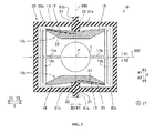
- the vibrating mirror device 100 may comprise: a mirror portion 1, which may have an external shape formed in essentially a circular shape, for reflecting light; a horizontal driving unit 10 for causing the mirror portion 1 to reciprocate around an axis 200 (the Y axis); and a pair of vertical driving units 51 and 52 for causing the entirety of the horizontal driving unit 10, including the mirror portion 1, to reciprocate around an axis 300 (the X axis).
- the horizontal driving unit 10 has the role of scanning the light that is reflected by the mirror portion 1 in the sideways direction (the horizontal direction) of a display region such as a screen, or the like, not shown.
- the vertical driving units 51 and 52 may have the role of sequentially moving, in the vertical direction, with each scan in the horizontal direction, the reflected light that is scanned in the horizontal direction.
- the horizontal driving unit 10 is an example of a "first driving portion" according to one or more embodiments of the present invention
- the vertical driving units 51 and 52 are an example of a "second driving portion” according to one or more embodiments of the present invention.
- the axis 200 and the axis 300 are, respectively, examples of a "first axis" and a "second axis" according to one or more embodiments of the present invention.
- the vibrating mirror device 100 may further comprise a supporting portion 30 for supporting the entirety of the horizontal driving unit 10 so as to enable reciprocation.
- the vibrating mirror device 100 may also comprise a supporting portion 60 for supporting the vertical driving units 51 and 52 so as to enable reciprocation in the X-Y plane.
- the horizontal driving unit 10 that includes the mirror portion 1, and the vertical driving units 51 and 52 may be formed having integrated structures from a base portion 15 made, for example, from Si (e.g., a Si substrate), as described below.
- the supporting portion 30 may have a frame shape that surrounds the outer peripheral portion of the horizontal driving unit 10 on four edges. Additionally, in the supporting portion 30, an edge portion 30a on one side (the X1 side) along the axis 300 may be connected to the vertical driving unit 51, and an edge portion 30b on the other side (the X2 side) may be connected to the vertical driving unit 52. Moreover, the horizontal driving unit 10 disposed on the inside of the supporting portion 30 may be connected to the edge portions 30a and 30b of the supporting portion 30 through connecting portions 31a and 31b, described below, that are formed on the axis 300.
- the supporting portion 60 may have a frame shape that surrounds, on four edges, the outer peripheral portion of a region wherein the vertical driving unit 51, the supporting portion 30 (the horizontal driving unit 10), and the vertical driving unit 52 may be disposed in that order from the X1 side toward the X2 side along the axis 300. Additionally, an end portion 51a of the vertical driving unit 51 may be connected to an edge portion 60a on one side (the Y1 side) of the supporting portion 60 along the axis 200, and an end portion 52a of the vertical driving unit 52 may be connected to an edge portion 60b on the other side (the Y2 side) of the supporting portion 60 along the axis 200.
- the vibrating mirror device 100 may be structured so that the horizontal driving unit 10 is driven (reciprocated) by a specific driving pattern, and the vertical driving units 51 and 52 are driven by a specific pattern to tilt the mirror portion 1 freely in relation to the X-Y plane, centered on the center point P.
- the structure may be such that the reflected light emitted from a light source portion 130 (referencing FIG. 7 ) and reflected by the mirror portion 1 is scanned in two axial directions (the X axial direction and the Y axial direction) by the tilt of the mirror portion 1.
- Piezoelectric elements e.g., crystals 17, which may be made from lead zirconium titanate (PZT) and a dielectric (a ferroelectric), are built into the horizontal driving unit 10, the vertical driving unit 51, and the vertical driving unit 52, where the piezoelectric crystals 17 of the individual driving portions may undergo bending deformation, and the tilt of the mirror portion 1 relative to the X-Y plane may be controlled, through application, to the piezoelectric crystal 17, of a voltage controlled to a specific pattern.
- PZT lead zirconium titanate
- a ferroelectric ferroelectric
- the horizontal driving unit 10 may include: torsion bars 11a and 11b that connect to the mirror portion 1 on the axis 200 (the Y axis) so as to enable reciprocation; a parallel bar 12a (on the Y1 side) and a parallel bar 12b (on the Y2 side) that can undergo flexural deformation and are connected to each of the torsion bars 11a and 11b; and driving portions 13a and 13b that are connected respectively to both end portions (on the X1 side and the X2 side) of the parallel bars 12a and 12b.
- the driving portion 13a and the driving portion 13b have essentially symmetrical shapes and structures, with the axis 200 as the line of symmetry.
- the driving portions 13a and 13b may be structured so as to each undergo flexural deformation through the application of a voltage to a piezoelectric crystal 17 (referencing FIG. 5 ).
- the piezoelectric crystal 17 may be a piezoelectric element that is polarized in the direction of film thickness (the Z direction), where the top surface 17a side or the bottom face 17b side undergoes deformation through expanding or contracting in the Y direction that, depending on the polarity, when a voltage is applied.
- the piezoelectric crystal 17 may have the property of the top face 17a side contracting relative to the bottom face 17b side, or, conversely, the bottom face 17b side contracting relative to the top face 17a side, through controlling the polarity (positive or negative) of the voltage that is applied to the piezoelectric crystal 17.
- the driving portions 13a and 13b are an example of a "first driving portion" according to one or more embodiments of the present invention.
- the structure may be such that when respective voltages are applied to the piezoelectric crystal 17 of the driving portion 13a and the piezoelectric crystal 17 of the driving portion 13b to drive (deform) the driving portions 13a and 13b with a specific pattern, the dislocation thereof is transmitted to the parallel bars 12a and 12b linked to the driving portions 13a and 13b, further causing the torsion bars 11a and 11b to undergo flexural deformation around the axis 200, to thereby cause the mirror portion 1 to reciprocate in the A1 direction and the A2 direction, relative to the supporting portion 30, with the axis 200 as the rotational axis.
- the mirror portion 1 may reciprocate while tilting in the A1 direction and the A2 direction with tilt angles that are greater than the tilt angles of the parallel bars 12a and 12b, due to a resonant effect.
- the driving portion 13a may be connected to the edge portion 30a (on the X1 side) of the supporting portion 30 through a connecting portion 31a, which is the stationary end, on the axis 300
- the driving portion 13b may be connected to the edge portion 30b (on the X2 side) of the supporting portion 30 through a connecting portion 31b, which is the stationary end, on the axis 300.
- the vertical driving unit 51 disposed on the X1 side of the horizontal driving unit 10 may include a driving portion 51c wherein the end portion 51a that is a stationary end is connected to an edge portion 60a (on the Y1 side) of the supporting portion 60, and an end portion 51b is connected to the connecting portion 31a of the supporting portion 30.
- the driving portion 51c may have a structure that has five deforming portions 51d that each extend in straight line shapes in the Y direction, where the individual deforming portions 51d are connected together at end portion regions (on the Y1 side or the Y2 side) in the lengthwise direction.
- the driving portion 51c may extend in a serpentine pattern on the X-Y plane in the Y direction in a state wherein the five deforming portions 51d are connected sequentially, with the end portion 51a connected to the edge portion 60a of the supporting portion 60 as the starting point, and the end portion 51b may be connected to the connecting portion 31a of the supporting portion 30.
- piezoelectric crystals 17 may be provided in each individual deforming portion 51d.
- the driving portion 51c (the vertical driving unit 51)
- the structure may be such that the five deforming portions 51d are deformed (driven) independently of each other through the application, to the individual piezoelectric crystals 17, of the voltages that are controlled in a specific pattern.
- the driving portion 51c is an example of a "second driving portion" according to one or more embodiments of the present invention.
- the vertical driving unit 52 disposed on the X2 side of the horizontal driving unit 10 may include a driving portion 52c wherein the end portion 52a which may be a stationary end may be connected to an edge portion 60b of the supporting portion 60, and an end portion 52b may be connected to the connecting portion 31b of the supporting portion 30.
- This driving portion 52c may also have the same structure as the driving portion 51c. That is, regarding the driving portion 52c, the five deforming portions 52d may be sequentially connected and have a serpentine pattern along the Y direction in the X-Y plane.
- the structure may be such that the five deforming portions 52d are deformed (driven) independently of each other through the application, to the individual piezoelectric crystals 17, of the voltages that are controlled in a specific pattern.
- the driving portion 52c is an example of a "second driving portion" according to one or more embodiments of the present invention.
- the vertical driving unit 51 and the vertical driving unit 52 may have essentially point-symmetrical shapes centered on the center point P of the mirror portion 1. That that is, there may be a relationship wherein rotating the driving portion 51c of the vertical driving unit 51 180° around the center R of the mirror portion 1 would cause it essentially to overlap the driving portion 52c of the vertical driving unit 52.
- the driving portions 51c and 52c may be structured so as to each individually undergo flexural deformation through the application of voltages to the individual piezoelectric crystals 17 (referencing FIG. 5 ).
- the driving portions 51c and 52c are driven (deformed) in a specific pattern, the dislocation thereof may be transmitted to the supporting portion 30, causing the supporting portion 30 to reciprocate around the axis 300.
- the structure may be such that the mirror portion 1 reciprocates in the B1 and B2 directions, relative to the supporting portion 60 (the X-Y plane), with the axis 300 as the rotational axis.
- the horizontal driving unit 10 may be driven at a predetermined frequency, for example of about 30 kHz, and may be structured so as to cause the mirror portion 1 and the torsion bars 11a and 11b to resonate.
- the vertical driving portion 50 may be driven at a predetermined frequency, for example of about 60 Hz, and may be structured so that the mirror portion 1 and the torsion bars 11a and 11b do not resonate.
- the supporting portion 60 may be structured so as to not deform, even when voltages are applied to the driving portions 51c and 52c.
- the horizontal driving unit 10 will be used as an example in the below, and the cross-sectional structure of the driving portion 13a (13b) will be explained.
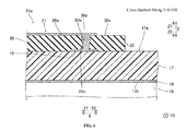
- the driving portion 13a on one side in the horizontal driving unit 10 may include: a base portion 15; a bottom electrode 16 formed on the top face (the Z1 side) of the base portion 15; a piezoelectric crystal 17 formed on top (the Z1 side) of the top face of the bottom electrode 16, a driving electrode 18 (referencing FIG. 5 ) formed on top (the Z1 side) of a top face 17a of the piezoelectric crystal 17; and a detecting electrode 19 formed in a region other than that of the driving electrode 18, on top (the Z1 side) of the top face 17a.
- the base portion 15 may be made, for example, from a Si substrate and may have a predetermined thickness (in the Z direction), for example between about 10 ⁇ m and 100 ⁇ m.
- the bottom electrode 16 may be made, for example, from Pt or a Cr-Au alloy and may have a predetermined thickness (in the Z direction), for example of between about 0.01 ⁇ m and about 0.5 ⁇ m.
- the piezoelectric crystal 17 made from PZT may have a predetermined thickness (in the Z direction), for example between about 1 ⁇ m and about 5 ⁇ m.
- the driving electrode 18 and the detecting electrode 19 may be made, for example, from Pt or a Cr-Au alloy, and may have predetermined thicknesses (in the Z direction), for example of between about 0.01 ⁇ m and about 0.5 ⁇ m.
- the driving electrode 18 (referencing FIG. 5 ) may be formed so as to contact the top face 17a of the piezoelectric crystal 17, provided so as to cause the piezoelectric crystal 17 to deform to the application of a voltage between itself and the bottom electrode 16.
- the detecting electrode 19 (referencing FIG. 6 ) may be structured so as to contact the top face 17a of the piezoelectric crystal 17, and provided in order to detect the potential difference (a voltage) between itself and the bottom electrode 16 accompanying the deformation of the piezoelectric crystal 17 when the mirror portion 1 is driven.
- an insulating layer 20 may be formed on top of the top face 17a of the piezoelectric crystal 17 in the driving portion 13a.
- the insulating layer 20 may be made, for example, from a polyimide resin, or from any other resin which can undergo flexural deformation and has a relatively low dielectric constant.
- the insulating layer 20 may have a predetermined thickness, for example between about 1 ⁇ m and about 30 ⁇ m, and may be formed through coating onto the top of the top face 17a of the piezoelectric crystal 17, for example through spin coating.
- the insulating layer 20 may be formed so as to cover the top face 17a of the piezoelectric crystal 17 wherein the driving electrode 18 and the detecting electrode 19 are not formed, and to cover the top faces of the driving electrode 18 and the detecting electrode 19.
- a lead interconnection 21 may be formed and disposed on top of the top face 20a of the insulating layer 20, connecting to the detecting electrode 19.
- the lead interconnection 21 may be made, for example, from Pt or a Cr-Au alloy, in the same manner as the detecting electrode 19, and may have a predetermined thickness, for example of between about 0.01 ⁇ m and about 0.5 ⁇ m.
- the lead interconnection 21 is an example of a "first lead interconnection" according to one or more embodiments of the present invention.
- the insulating layer 20 may be formed so as to cover the detecting electrode 19 on the top of the top face 17a of the piezoelectric crystal 17, and the lead interconnection 21 may be connected to the detecting electrode 19 through a through hole 20b that passes through the insulating layer 20, in the direction of thickness, at a part that corresponds to the detecting electrode 19.
- This through hole 20b may be formed, for example, using photolithography on the insulating layer 20, which is formed coating the top of the top face 17a of the piezoelectric crystal 17, in the part that covers the detecting electrode 19.
- the through hole 20b may have an inside surface 20d with a tapered shape so that the opening area (the opening diameter) at the interfacial portion 20c (the contact portion) with the detecting electrode 19 is smaller than the opening area (the opening diameter) on the top face 20a side.
- the inside surface 20d may be formed with a smooth slope (inclined) shape as a result of the opening at the top face 20a side being wider than the opening at the interfacial portion 20c side due to the slight contraction of the insulating layer 20 at the top face 20a side in curing (baking) after the through hole 20b is formed through exposure.
- an interconnection pattern may be formed for example using sputtering, or the like, on the insulating layer 20.
- the metal material may be deposited in the through hole 20b, to connect the lead interconnection 21 to the detecting electrode 19.
- the through hole 20b is an example of a "hole portion" according to one or more embodiments of the present invention.
- a lead interconnection 22 that is disposed on top of the top face 20a of the insulating layer 20 and that connects to the driving electrode 18 through a through hole 20b may be formed in the driving portion 13a separately from the lead interconnection 21.
- the lead interconnection 22 may be made, for example, from Pt or a Cr-Au alloy, in the same manner as the driving electrode 18, and may have a predetermined thickness, for example of between about 0.01 ⁇ m and about 0.5 ⁇ m.
- the lead interconnection 22 is an example of a "second lead interconnection" according to one or more embodiments of the present invention.
- the driving electrode 18 may be formed so as to cover most parts of the planar face shape (the shape of the top face 17a) of the piezoelectric crystal 17, for example more than 50% or 60% or 70% or 80% or 90% thereof.
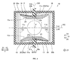
- the detecting electrode 19, having for example a long thin shape may be formed on the top face 17a of the piezoelectric crystal 17 wherein the driving electrode 18 is not formed, with a gap portion 23, which has a portion that may be bent, therebetween.
- the piezoelectric crystal 17 may be exposed only in the gap portion 23.
- a bottom electrode 16 (referencing FIG. 5 ), formed so as to have the same planar shape as the planar shape of the piezoelectric crystal 17, and a base portion 15 (referencing FIG. 5 ), may be formed in that order.
- the insulating layer 20 may be formed so as to cover a specific region of the driving portion 13a.
- the insulating layer 20 may be formed so as to cover a region of the top face 17a of the piezoelectric crystal 17 that is the part wherein the detecting electrode 19 is formed, and so as to cover a region of the top face 17a of the piezoelectric crystal 17 that is the part where in the driving electrode 18 is formed, and extend to the end portion 51b of the vertical driving unit 51 (the driving portion 51c), cutting across the edge portion 30a (on the X1 side) of the supporting portion 30 on the outside of the driving portion 13a from the connecting portion 31a (on the X1 side) formed on the axis 300.
- the insulating layer 20, as illustrated in FIG. 1 may be formed extending sequentially to the region wherein the end portion 51a of the driving portion 51c and the edge portion 60a of the supporting portion 60 connect, through the five deforming portions 51d (on the front side of the paper) from the end portion 51b of the driving portion 51c.
- the through hole 20b may be formed in the insulating layer 20 passing through the insulating layer 20 in the direction of thickness at the part that corresponds to the detecting electrode 19, and the through hole 20e (referencing FIG. 5 ) may be formed passing through the insulating layer 20 in the direction of thickness at the part corresponding to the driving electrode 18.
- the through hole 20e that is adjacent to the through hole 20b, on the Y2 side, may be formed in the same manner as the through hole 20b. Consequently, as illustrated in FIG. 4 , the top face of the driving electrode 18 may be exposed on the inside of the through hole 20b, and the top face of the detecting electrode 19 may be exposed on the inside of the through hole 20e.
- the lead interconnection 21, described above may connect to the detecting electrode 19 through the through hole 20b, and the lead interconnection 22 may connect to the driving electrode 18 through the through hole 20e.
- the lead interconnection 21 may be connected to the detecting electrode 19 of the driving portion 13a and lead out from the detecting electrode 19 across the top face 20a of the insulating layer 20 formed on top of the top face of the driving portion 51c (the piezoelectric crystal 17) that may structure the vertical driving unit 51 (on the X1 side) to extend to the edge portion 60a of the supporting portion 60. That is, the lead interconnection 21 may be formed continuously from the driving portion 13a part through the connecting portion 31a, cutting across the edge portion 30a of the supporting portion 30, along the insulating layer 20, in a serpentine pattern, along with the driving portion 51c, to arrive at the edge portion 60a of the supporting portion 60.
- the interconnection length (the total extension distance) of the lead interconnection 21 may be greater than the length of the lengthwise direction (the Y direction) of the detecting electrode 19.
- the edge portion 60a of the supporting portion 60 is an example of an "outer region" according to one or more embodiments of the present invention.
- the structure of the lead interconnection 22 may be the same as for the lead interconnection 21, where the lead interconnection 22 connects to the detecting electrode 19 of the driving portion 13a and leads out from the driving electrode 18 over the top of the top face 20a of the insulating layer 20 formed on the top face of the piezoelectric crystal 17 of the vertical driving unit 51, to extend to the edge portion 60a of the supporting portion 60. That is, the lead interconnection 22 may also be formed continuously from the driving portion 13a part through the connecting portion 31 a, cutting across the edge portion 30a of the supporting portion 30, along the insulating layer 20, in a serpentine pattern, along with the driving portion 51c, to arrive at the edge portion 60a of the supporting portion 60.
- Wire bonding portions 21a and 22a may be formed respectively in the lead interconnections 21 and 22. Moreover, the structure may be such that lead wires (electrical interconnections) for a dislocation detecting portion, not shown, can be connected to the wire bonding portions 21a and 22a.
- the vibrating mirror device 100 may have a structure such that, after the lead interconnections 21 and 22 lead out from the respective driving portions 13a and 13b, progressing in parallel on the top face 20a of the insulating layer 20, the lead interconnections 21 and 22 extend along the top face 20a of the insulating layer 20 over the vertical driving units 51 and 52, respectively, to the edge portions 60a and 60b of the supporting portion 60.
- the edge portion 60b of the supporting portion 60 is an example of an "outer region" according to one or more embodiments of the present invention.
- the five deforming portions 51d that may structure the driving portion 51c (on the X1 side) of the vertical driving unit 51 and the five deforming portions 52d that may structure the driving portion 52c (on the X2 side) of the vertical driving unit 52 may be structured so as to have cross-sectional structures that are essentially identical to the cross-sectional structures of the driving portions 13a and 13b that structure the horizontal driving unit 10, as illustrated in FIG. 1 . That is, in the deforming portion 51d, the bottom electrode 16 on the top face of the substrate 15, the piezoelectric crystal 17, the driving electrode 18, and the detecting electrode 19 may be formed having the layered structure illustrated in FIG. 5 .
- the lead interconnections (not shown) from the driving electrodes 18 for the deforming portions 51d and from the detecting electrode 19 may be formed on top of the top face 17a of the piezoelectric crystal 17 with the insulating layer 20 interposed therebetween.
- all of the deforming portions 51d and 52d may have such a cross-sectional structure, and the lead interconnections from the driving electrode 18 and the detecting electrode 19 may be structured so as to pass over the top face 20a of the insulating layer 20, to extend to the supporting portion 60.
- the vibrating mirror device 100 may be structured so as to be incorporated into a portable projector 160.
- the portable projector 160 may comprise: a vibrating mirror device 100 for scanning a laser beam; a controlling portion 120 for analyzing video inputted from the outside through a terminal portion 110 to recognize pixel information; a red LD (laser diode) portion 131 for emitting a red laser beam, a blue LD portion 132 for emitting a blue laser beam, and a green LD portion 133 for emitting a green laser beam, as a light source portion 130; a laser beam controlling portion 140 for controlling the gradations of the laser beams emitted by the red LD portion 131, the blue LD portion 132, and the green LD portion 133 based on pixel information recognized by the controlling portion 120; and a dislocation detecting portion 150 for detecting the dislocation of each individual driving portion in the vibrating mirror device 100 when driven.
- the red LD portion 131 for scanning a laser beam
- a controlling portion 120 for
- the operational control of the vibrating mirror device 100 may be performed while the amounts of deformation of the piezoelectric crystals 17 in the individual driving portions (the driving portion 13a, the driving portion 13b, the driving portion 51c, and the driving portion 52c) are detected by the dislocation detecting portion 150 when the mirror portion 1 is reciprocated around two axes (the X axis and the Y axis), to scan, two-dimensionally, the laser beam from the portable projector 160 on a display region such as a screen, not shown.
- the lead interconnections from the individual driving portions (the lead interconnections 21 (referencing FIG.
- the driving portion 13a and the driving portion 13b) may be disposed along the top face 20a of the insulating layer 20, which is separated from the piezoelectric crystal 17, and thus the discharge (diffusion) into the lead interconnection 21 of the surface charge that is produced in the part at the detecting electrode 19 (referencing FIG. 5 ) may be greatly prevented.
- the voltage value detected at the part of the detecting electrode 19 may be detected in the dislocation detecting portion 150 without a voltage drop, making it possible to reflect, into operational control of the vibrating mirror device 100, a state wherein the amounts of deformation of the piezoelectric crystal 17 of each of the individual driving portions (the driving portion 13a, the driving portion 13b, the driving portion 51c, and the driving portion 52c) are detected accurately.
- the insulating layer 20 formed on top of the top face 17a of the piezoelectric crystal 17 and the lead interconnection 21 formed on top of the top face 20a of the insulating layer 20, connected to the detecting electrode 19, and that extends to the region outside of the driving portions 13a and 13b (the edge portions 60a and 60b of the supporting portion 60) make it possible to lead out the lead interconnection 21, which may be connected to the detecting electrode 19, along the top face 20a of the insulating layer 20, which may be separated from the piezoelectric crystal 17, to a region on the outside of the driving portions 13a and 13b without contacting the top face 17a of the piezoelectric crystal 17 on which the detecting electrode 19 is formed.
- the amount of deformation of the piezoelectric crystal 17 may be detected through the detecting electrode 19 in a state wherein only the detecting electrode 19 part is in contact with the top face 17a of the piezoelectric crystal 17, regardless of the length of the lead interconnection 21.
- the lead interconnection 21 may be separated from the piezoelectric crystal 17 by the insulating layer 20, making it possible to prevent the discharge (diffusion), into the lead interconnection 21, of the surface charge produced at the part of the detecting electrode 19, affected by also by the piezoelectric crystal 17 disposed on the bottom layer side (the Z2 side) of the lead interconnection 21.
- the detecting electrode 19 it is possible to prevent the detection, by the detecting electrode 19, of a voltage value in a state wherein there has been a voltage drop caused by the discharge of the surface charge. Moreover, because the electrode value detected by the detecting electrode 19 part is in a state wherein there is no voltage drop, the amounts of deformation in the piezoelectric crystal 17 of the driving portion 13a and the piezoelectric crystal 17 of the driving portion 13b can be detected accurately.
- the insulating layer 20 may be formed so as to cover the detecting electrode 19 on the top of the top face 17a of the piezoelectric crystal 17, and the lead interconnection 21 may be connected to the detecting electrode 19 through a through hole 20b that passes through the insulating layer 20, in the direction of thickness, at a part that corresponds to the detecting electrode 19.
- the driving portions 13a and 13b may be structured so as to undergo flexural deformation during driving, and the insulating layer 20 may be formed from a resin that can undergo flexural deformation.
- the insulating layer 20 made from the resin that can undergo flexural deformation may be formed on top of the top faces 17a of the respective piezoelectric crystals 17 of the driving portions 13a and 13b, making it possible, for example, to prevent the insulating layer 20 from resisting the respective deformations of the driving portions 13a and 13b, even when the piezoelectric crystal 17 undergoes bending deformation (flexural deformation).
- the use of a polyimide resin that has a relatively small dielectric constant for the resin makes it possible to control effectively the effect of the lead interconnection 21 on the surface charge of the piezoelectric crystal 17 that is at a layer below than that of the polyimide resin.
- the driving portion 13a (13b) may be formed so as to contact the top face 17a of the piezoelectric crystal 17, and include a driving electrode 18 for applying a voltage to cause the piezoelectric crystal 17 to undergo flexural deformation, to drive the mirror portion 1.
- the vibrating mirror device 100 may further comprise a lead interconnection 22 formed on top of the top face 20a of the insulating layer 20, connecting to the driving electrode 18 of the driving portion 13a (13b), and extending to the outer region (the edge portions 60a and 60b) of the driving portion 13a (13b).
- the lead interconnection 22 connected to the driving electrode 18 may also lead out, to an outside region (the edge portions 60a and 60b of the supporting portion 60), by extending over the top face 20a of the insulating layer 20, which is separated from the piezoelectric crystal 17, without contacting the top face 17a of the piezoelectric crystal 17 whereon the driving electrode 18 is formed. That is, in addition to the lead interconnection 21, a lead interconnection 22 may lead out similarly to an outer region further than the driving portion 13a (13b), so as to eliminate the need to perform wire bonding of the lead lines (outer interconnections) at a location in the vicinity of the driving portion 13a (13b). Consequently, this makes it possible, for example, to avoid reliably damage to the horizontal driving unit 10 (the driving portions 13a and 13b) that is caused by the wire bonding.
- the insulating layer 20 may be formed so as to cover a region of a portion that includes the detecting electrode 19 on the top face 17a of the piezoelectric crystal 17.
- the insulating layer 20 may be formed on only that part of the entire surface (the top face 17a) of the piezoelectric crystal 17 whereon the detecting electrode 19 is formed, so that, to that extent, the stress of the insulating layer 20 does not greatly affect the flexural deformation of the piezoelectric crystal 17. This makes it possible, for example, to prevent effectively reduction in the deformation force of the piezoelectric crystal 17 that would be caused by stress in the insulating layer 20.
- the detecting electrode 19 may have a long thin shape that extends in a specific direction (the Y direction), and the interconnection length (the total length) of the lead interconnection 21 may be longer than the length of the lengthwise direction (the Y direction) of the detecting electrode 19.
- the lead interconnection 21 may extend along the top face 20a of the insulating layer 20, which is separated from the piezoelectric crystal 17, making it possible to prevent the discharge of the surface charge, produced at that part of the detecting electrode 19, to the lead interconnection 21, which has a long interconnection length (a large interconnection surface area).
- one or more embodiments of the present invention may include a horizontal driving unit 10 for driving the mirror portion 1 around the axis 200, and vertical driving units 51 and 52, for driving the mirror portion 1 around the axis 300, which may be perpendicular to the axis 200.
- the lead interconnection 21 may be connected to the detecting electrode 19 of the horizontal driving unit 10 and may lead out from the detecting electrode 19 across the top face of the insulating layer 20 formed on top of the top face of the piezoelectric crystals 17 that may structure the vertical driving units 51 and 52, to lead out to the outside.
- an insulating layer 20 may be interposed between the lead interconnection 21 and the piezoelectric crystals 17 of the vertical driving units 51 and 52, making it possible, for example, to greatly prevent the discharge (diffusion) of the surface charge produced at the detecting electrode 19 part of the horizontal driving unit 10 into the lead interconnection 21, affected by the piezoelectric crystals (dielectrics) of the vertical driving units 51 and 52.
- the application of the vibrating mirror device 100 to the portable projector 160 enables the driving of the vibrating mirror device 100 to be controlled by a controlling portion 120 such that the amounts of deformation of the piezoelectric crystals 17 are detected accurately, thus enabling projection, onto a display region, such as a screen, or the like, of a video in a state wherein the laser beam from the light source portion 130 is scanned with precision.
- the present invention is not limited thereto.
- the resin has a low dielectric constant and can undergo flexural deformation
- the insulating layer 20 may be formed using, for example, urethane resin.
- the base portion 15 was structured from a Si substrate
- the present invention is not limited thereto.
- the base portion 15 may instead be structured using a metal material, such as stainless steel.
- the present invention is not limited thereto.
- the detecting electrode 19 may be structured using a metal material having conductivity such as, for example, Al, Cu, or Au, rather than the above.
- the lead interconnection 21 was structured using Pt or a Cr-Au alloy in the same manner as the detecting electrode 19 was set forth above, the present invention is not limited thereto.
- the lead interconnection 21 may be structured using a metal material having conductivity such as, for example, Al, Cu, or Au, rather than the above.
- the piezoelectric crystal 17 is made from lead zirconium titanate (PZT)
- PZT lead zirconium titanate
- the present invention is not limited thereto.
- a piezoelectric material made from oxides having lead, titanium, and zirconium as the primary components thereof, or a piezoelectric material such as zinc oxide (ZnO), lanthanum lead zirconate titanate ((Pb, La) (Zr, Ti))O 3 ), potassium niobate (KNbO 3 ), sodium niobate (NaNbO 3 ), or the like may be used to structure the piezoelectric crystal 17.
- a bottom electrode 16 that is disposed on the bottom face 17b of the piezoelectric crystal 17 is formed on essentially the entire face of the driving portion 13a (13b) and electrodes that are disposed on the top face 17a of the piezoelectric crystal 17 are divided into a driving electrode 18 and a detecting electrode 19
- the present invention is not limited thereto.
- the electrode that is disposed on the top face 17a of the piezoelectric crystal 17 may be formed on essentially the entire surface of the driving portion 13a (13b), and electrodes that are disposed on the bottom face 17b of the piezoelectric crystal 17 may be divided into a driving electrode 18 and a detecting electrode 19.
- the present invention is not limited thereto.
- the structure may be of only the horizontal driving unit 10 without the vertical driving unit 51 (52), so that the vibrating mirror device is structured so as to scan the light in only one dimension.
- certain "units" or "portions" of one or more embodiments of the present invention may be implemented by a circuit, processor, etc. using known methods.
Landscapes
- Physics & Mathematics (AREA)
- Optics & Photonics (AREA)
- General Physics & Mathematics (AREA)
- Engineering & Computer Science (AREA)
- Multimedia (AREA)
- Signal Processing (AREA)
- Mechanical Optical Scanning Systems (AREA)
- Mechanical Light Control Or Optical Switches (AREA)
- Micromachines (AREA)
Abstract
Description
- The present invention relates generally to a vibrating mirror device and an electronic device having a projector function, e.g., a vibrating element and an electronic device having a projector function that is provided with a driving portion that includes a detecting electrode for detecting an amount of deformation in a piezoelectric element (e.g., crystal).
- Conventional vibrating mirror devices are provided with driving portions that include detecting electrodes for detecting an amount of deformation of a piezoelectric crystal (referencing, for example, Patent Citation 1).
-
Patent Citation 1 discloses a single-axis optical scanner (vibrating mirror device) comprising an essentially circular mirror portion and a cantilever (a bar that is held on one end) elastic portion wherein the free end is connected to the mirror portion and the stationary end is connected to a stationary frame. In the optical scanner set forth inPatent Citation 1, a piezoelectric crystal is formed in a state where it is held between a top electrode and a bottom electrode in a specific location of the elastic portion. The structure is such that a single piezoelectric crystal is provided with two sets of top electrodes and bottom electrodes, where the piezoelectric crystal is driven by applying a voltage between the top electrode and the bottom electrode on one side, and the potential difference between the electrodes accompanying deformation of the piezoelectric crystal is detected using the top electrode and the bottom electrode on the other side. Moreover, the structure is such that the top electrodes and bottom electrodes extend from the elastic portion to a stationary frame at some distance, where the external interconnections for the power supply and the interconnections from a displacement detecting circuit are respectively wire-bonded to the top electrodes and the bottom electrodes at a part of the stationary frame. - [Patent Document 1] Japanese Unexamined Patent Application Publication
2009-163154 - In the optical scanner set forth in
Patent Citation 1, the structure is intended to cause a mirror portion to reciprocate around a single axis, thus making it possible to connect the interconnections from the dislocation detecting circuit and the like to the top electrode and the bottom electrode at the stationary frame part. On the other hand, in the case of an optical scanner (a vibrating mirror device) wherein the mirror portion disposed in a center portion of the element reciprocates around two mutually perpendicular axes, with respect to the top electrode and the bottom electrode (the detecting electrodes) for detecting the amount of deformation (the potential difference) for the driving portion for the first axis, it is necessary for the detecting electrodes to lead out to a stationary frame that is to the outside of not only the driving portion for the first axis but also the driving portion for the second axis (the driving portion for the first axis causes the mirror portion to reciprocate around the first axis, and the driving portion for the second axis causes the mirror portion to reciprocate around the second axis). In this case, the interconnections for leading out from the detecting electrodes are formed in the same layer as the detecting electrodes for the piezoelectric crystal, through patterning or the like, to lead out to the outside. - However, when not only the detecting electrodes but also the parts for the top and bottom lead interconnections face each other with the piezoelectric crystal (a dielectric body) held therebetween, the surface charge charged at the part where the detecting electrode accompanying deformation of the piezoelectric crystal is affected by the piezoelectric crystal so as to discharge (diffuse) into the lead interconnections. Because of this, even if a surface charge is produced in the detecting electrode in an amount in accordance with the deformation of the piezoelectric crystal, a voltage value (a potential difference) will be detected by the detecting electrode in a state wherein a voltage drop was caused by the surface charge discharging into the lead interconnections. Moreover, because the detecting electrode will actually detect a voltage value smaller than the voltage value of that should be detected, accurate detection of the amount of deformation of the piezoelectric crystal is difficult.
- One or more embodiments of the present invention provide a vibrating mirror device able to suppress deformation of the mirror portion, and an electronic device having a projector function, provided with the vibrating mirror device.
- Further, one or more embodiments of the present invention provide a vibrating mirror device and an electronic device having a projector function so as to prevent a voltage value from being detected by the detecting electrodes in a state wherein there has been a voltage drop caused by the discharge of the surface charge.
- According to one or more embodiments, a vibrating mirror device may comprise a mirror portion, a driving portion including a detecting electrode configured to detect an amount of deformation of a piezoelectric element when driving the mirror portion by applying a voltage to cause the piezoelectric element to deform, an insulating layer, and a first lead interconnection. According to one or more embodiments, the mirror portion may comprise a mirror. According to one or more embodiments, the driving portion may comprise a driving circuit. According to one or more embodiments, the insulating layer may be formed on a top face of the piezoelectric element. According to one or more embodiments, the first lead interconnection is formed on the top face of the insulating layer. According to one or more embodiments, the first lead interconnection is configured to contact the detecting electrode. According to one or more embodiments, the first lead interconnection extends to a region outside of the driving portion.
- According to one or more embodiments of the present invention, the insulating layer (which may be formed on the top face of the piezoelectric element) and the first lead interconnection (which may be formed on the top face of the insulating layer, may be connected to the detecting electrode, and may extend to a region outside of the driving portion) of the vibrating mirror device make it possible to lead out, to a region on the outside of the driving portion, the first lead interconnection connected to the detecting electrode along the top face of the insulating layer (which may be separated from the piezoelectric element, e.g., crystal) without contacting the top face of the piezoelectric element on which the detecting electrode is formed. As a result, the amount of deformation of the piezoelectric element (the voltage value produced through the piezoelectric effect) may be detected through the detecting electrode in a state wherein only the detecting electrode portion is in contact with the top face of the piezoelectric element, regardless of the length of the first lead interconnection. At this time, the first lead interconnection may be separated from the piezoelectric element by the insulating layer, so as to prevent the discharge (diffusion) of the surface charge produced at the part at the detecting electrode into the first lead interconnection, affected by the piezoelectric element disposed on the bottom layer side of the first lead interconnection as well. As a result, in one or more embodiments, it is possible to prevent detection, by the detecting electrode, of a voltage value in a state wherein there has been a voltage drop caused by the discharge of the surface charge. Moreover, in one or more embodiments, because the voltage value detected at the detecting electrode part may be detected in a state wherein there is no voltage drop, it is possible to detect with good accuracy the amount of deformation of the piezoelectric element (the driving portion).
- According to one or more embodiments, the insulating layer may be formed so as to cover the detecting electrode on the top face of the piezoelectric element. According to one or more embodiments, the first lead interconnection may be connected to the detecting electrode through a hole portion that passes through the insulating layer, in a thickness direction, at a part that corresponds to the detecting electrode. Structuring in this way may enable easy connection of the first lead interconnection, which may be formed on the top face of the insulating layer and may extend along the top face of the insulating layer, to a detecting electrode positioned on a layer below the insulating layer through a hole portion that passes through the insulating layer in the direction of thickness.
- According to one or more embodiments, the driving portion may be structured so as to undergo flexural deformation when driven. According to one or more embodiments, the insulating layer may be made from a resin capable of undergoing flexural deformation. With such a structure, the insulating layer formed from a resin that can undergo flexural deformation may be formed on the top face of the piezoelectric element, making it possible to prevent the insulating layer from resisting the deformation of the driving portion even when a driving portion that includes a piezoelectric element undergoes bending deformation (flexural deformation).
- According to one or more embodiments, the driving portion may further include a driving electrode, which may be formed so as to contact the top face of the piezoelectric element, for applying a voltage to cause the piezoelectric element to undergo flexural deformation to drive the mirror portion. According to one or more embodiments, the vibrating mirror device may further include a second lead interconnection. The second lead interconnection may be formed on the top face of the insulating layer, may be connected to the driving electrode of the driving portion, and may extend to a region outside of the driving portion. With such a structure, the second lead interconnection connected to the driving electrode can also lead out, to a region outside of the driving portion, by extending over the top face of the insulating layer, separated from the piezoelectric element, without contacting the top face of the piezoelectric element whereon the driving electrode is formed. That is, in addition to the first lead interconnection, a second lead interconnection may lead out similarly to an outer region that is further than the driving portion, so as to eliminate the need to perform wire bonding of the lead lines (outer interconnections) at a location in the vicinity of the driving portion. Consequently, this makes it possible, for example, to avoid reliably damage to the driving portion that is caused by the wire bonding.
- According to one or more embodiments, the insulating layer may be formed so as to cover a region of a portion that includes the detecting electrode on the top face of the piezoelectric element. With this structure, the insulating layer may be formed on only that part of the entire surface (top face) of the piezoelectric element whereon the detecting electrode is formed, so that, to that extent, the stress of the insulating layer does not greatly affect the flexural deformation of the piezoelectric element. This makes it possible, for example, to prevent effectively reduction in the deformation force of the piezoelectric element that would be caused by stress in the insulating layer.
- According to one or more embodiments, the detecting electrode may have a long thin shape that extends in a first direction. According to one or more embodiments, an interconnection length of the first lead interconnection may be greater than a length of the lengthwise direction of the detecting electrode. In this way, even in a case of detecting the amount of deformation of the piezoelectric element (the voltage value produced through the piezoelectric effect) through the first lead interconnection that leads out across an interconnection distance greater (longer) than the length of the lengthwise direction of the detecting electrode from the detecting electrode, the first lead interconnection may extend along the top face of the insulating layer, which is separated from the piezoelectric element, thus making it possible to prevent the discharge of the surface charge (produced at that part of the detecting electrode) to the first lead interconnection, which has a long interconnection length (a large interconnection surface area). As a result, for example, even when a first lead interconnection that has a long interconnection length is used, not only is it possible to detect the voltage value detected by the detecting electrode part, in a state wherein no extreme voltage drop occurs, but it is also possible to detect, with good accuracy, the amount of deformation of the piezoelectric element (the driving portion).
- According to one or more embodiments, the driving portion may include a first driving portion for causing the mirror portion to reciprocate around a first axis, and a second driving portion for causing the mirror portion to reciprocate around a second axis that is substantially perpendicular to the first axis. According to one or more embodiments, the insulating layer may be formed on the top face of the piezoelectric element across the first driving portion and the second driving portion. According to one or more embodiments, the first lead interconnection may lead out from the detecting electrode of the first driving portion and is routed sequentially over a top face of the insulating layer corresponding to the first driving portion and a top face of the insulating layer corresponding to the second driving portion, so as to lead out to a region outside of the second driving portion. With this structure, even when the first lead interconnection leads out to an outer region across a second driving portion, an insulating layer may be interposed between the first lead interconnection and the piezoelectric element of the second driving portion as well, in the same manner as with the first driving portion part, thus making it possible to prevent the discharge (diffusion) of the surface charge that is produced at the detecting electrode part of the first driving portion into the first lead interconnection, affected by the piezoelectric element of the second driving portion. As a result, for example, even in a vibrating mirror device wherein a mirror portion is caused to reciprocate around two axes (a first axis and a second axis) by a first driving portion and a second driving portion, it is possible to prevent effectively the detection, by the detecting electrode, of a voltage value in a state wherein a voltage drop has occurred due to discharge of the surface charge.
- According to one or more embodiments, an electronic device having a projector function may comprise: a laser beam producing portion configured to produce a laser beam; a controlling portion configured to analyze an inputted video to recognize pixel information; and a vibrating mirror device configured to scan the laser beam. According to one or more embodiments, the vibrating mirror device may be as described in any of the above-mentioned embodiments. For example, the vibrating mirror device may include: a mirror portion; a driving portion including a detecting electrode configured to detect an amount of deformation of a piezoelectric element when driving the mirror portion by applying a voltage to cause the piezoelectric element to deform; an insulating layer formed on a top face of the piezoelectric element; and a lead interconnection formed on the top face of the insulating layer and extending to a region outside of the driving portion, the first lead interconnection being configured to contact the detecting electrode of the driving portion.
- According to one or more embodiments of the present invention, the electronic device having the projector function may comprise a vibrating mirror device which may include an insulating layer formed on the top face of the piezoelectric element and the first lead interconnection (which may be formed on the top face of the insulating layer, connected to the detecting electrode, and extend to a region that is outside of the driving portion), which makes it possible to lead out, to a region on the outside of the driving portion, the lead interconnection connected to the detecting electrode along the top face of the insulating layer (which may be separated from the piezoelectric element) without contacting the top face of the piezoelectric element on which the detecting electrode is formed. As a result, for example, the amount of deformation of the piezoelectric element (the voltage value that is produced through the piezoelectric effect) may be detected through the detecting electrode in a state wherein only the detecting electrode portion is in contact with the top face of the piezoelectric element, regardless of the length of the lead interconnection. At this time, the lead interconnection may be separated from the piezoelectric element by the insulating layer so as to prevent the discharge (diffusion) of the surface charge produced at the part at the detecting electrode into the lead interconnection, affected by the piezoelectric element disposed on the bottom layer side of the lead interconnection as well. As a result, for example, in the vibrating mirror device, it is possible to prevent the detection, by the detecting electrode, of a voltage value in a state wherein there has been a voltage drop caused by the discharge of the surface charge. Moreover, because the voltage value detected at the detecting electrode part is detected in a state wherein there is no voltage drop, it is possible to detect with good accuracy the amount of deformation of the piezoelectric element (the driving portion). Consequently, the driving of the vibrating mirror device may be controlled in a state wherein the amount of deformation of the piezoelectric element is detected accurately, so that in the electronic device with the projector function, the laser beam can project an image in a state wherein the scanning is accurate.
- As described above, one or more embodiments of the present invention make it possible to prevent the detection, by the detecting electrode, of a voltage value in a state wherein there has been a voltage drop caused by the discharge of the surface charge.
-
-
FIG. 1 is a top view of the overall structure of a vibrating mirror device according to one or more embodiments of the present invention.FIG. 2 is a top view wherein part of the horizontal driving portion in the vibrating mirror device illustrated inFIG. 1 has been enlarged. -
FIG. 3 is a top view of a state wherein the lead interconnection and the insulating layer have been removed in the horizontal driving portion illustrated inFIG. 2 . -
FIG. 4 is a top view of the structure of the horizontal driving portion in a state wherein an insulating layer that has a through hole has been formed on the structure illustrated inFIG. 3 . -
FIG. 5 is a cross-section along the section 500-500 inFIG. 2 . -
FIG. 6 is a cross-section along the section 510-510 inFIG. 2 . -
FIG. 7 is a block diagram for a portable projector that includes a vibrating mirror device according to one or more embodiments of the present invention. - One or more embodiments of the present invention will be explained below based on the drawings.
- Structures for a vibrating
mirror device 100 and aportable projector 160 according to one or more embodiments of the present invention will be explained first in reference toFIG. 1 through FIG. 7 . In the below the structure of the vibrating mirror device 100 (referencingFIG. 1 ) will be explained first, and then an example of a structure of a portable projector 160 (referencingFIG. 7 ) comprising the vibratingmirror device 100 will be explained. Theportable projection 160 is an example of an "electronic device having a projector function" according to one or more embodiments of the present invention. - As illustrated in
FIG. 1 , the vibratingmirror device 100 according to according to one or more embodiments of the present invention may comprise: amirror portion 1, which may have an external shape formed in essentially a circular shape, for reflecting light; ahorizontal driving unit 10 for causing themirror portion 1 to reciprocate around an axis 200 (the Y axis); and a pair ofvertical driving units horizontal driving unit 10, including themirror portion 1, to reciprocate around an axis 300 (the X axis). Here thehorizontal driving unit 10 has the role of scanning the light that is reflected by themirror portion 1 in the sideways direction (the horizontal direction) of a display region such as a screen, or the like, not shown. Moreover, thevertical driving units horizontal driving unit 10 is an example of a "first driving portion" according to one or more embodiments of the present invention, and thevertical driving units axis 200 and theaxis 300 are, respectively, examples of a "first axis" and a "second axis" according to one or more embodiments of the present invention. - Moreover, the vibrating
mirror device 100 may further comprise a supportingportion 30 for supporting the entirety of thehorizontal driving unit 10 so as to enable reciprocation. The vibratingmirror device 100 may also comprise a supportingportion 60 for supporting thevertical driving units horizontal driving unit 10 that includes themirror portion 1, and thevertical driving units base portion 15 made, for example, from Si (e.g., a Si substrate), as described below. - Moreover, as illustrated in
FIG. 1 , the supportingportion 30 may have a frame shape that surrounds the outer peripheral portion of thehorizontal driving unit 10 on four edges. Additionally, in the supportingportion 30, anedge portion 30a on one side (the X1 side) along theaxis 300 may be connected to thevertical driving unit 51, and anedge portion 30b on the other side (the X2 side) may be connected to thevertical driving unit 52. Moreover, thehorizontal driving unit 10 disposed on the inside of the supportingportion 30 may be connected to theedge portions portion 30 through connectingportions axis 300. - Moreover, the supporting
portion 60 may have a frame shape that surrounds, on four edges, the outer peripheral portion of a region wherein thevertical driving unit 51, the supporting portion 30 (the horizontal driving unit 10), and thevertical driving unit 52 may be disposed in that order from the X1 side toward the X2 side along theaxis 300. Additionally, anend portion 51a of thevertical driving unit 51 may be connected to anedge portion 60a on one side (the Y1 side) of the supportingportion 60 along theaxis 200, and an end portion 52a of thevertical driving unit 52 may be connected to an edge portion 60b on the other side (the Y2 side) of the supportingportion 60 along theaxis 200. - As a result, the vibrating
mirror device 100 may be structured so that thehorizontal driving unit 10 is driven (reciprocated) by a specific driving pattern, and thevertical driving units mirror portion 1 freely in relation to the X-Y plane, centered on the center point P. Given this, the structure may be such that the reflected light emitted from a light source portion 130 (referencingFIG. 7 ) and reflected by themirror portion 1 is scanned in two axial directions (the X axial direction and the Y axial direction) by the tilt of themirror portion 1. Piezoelectric elements, e.g.,crystals 17, which may be made from lead zirconium titanate (PZT) and a dielectric (a ferroelectric), are built into thehorizontal driving unit 10, thevertical driving unit 51, and thevertical driving unit 52, where thepiezoelectric crystals 17 of the individual driving portions may undergo bending deformation, and the tilt of themirror portion 1 relative to the X-Y plane may be controlled, through application, to thepiezoelectric crystal 17, of a voltage controlled to a specific pattern. - Moreover, as illustrated in
FIG. 2 , thehorizontal driving unit 10 may include:torsion bars mirror portion 1 on the axis 200 (the Y axis) so as to enable reciprocation; aparallel bar 12a (on the Y1 side) and aparallel bar 12b (on the Y2 side) that can undergo flexural deformation and are connected to each of thetorsion bars portions parallel bars portion 13a and the drivingportion 13b have essentially symmetrical shapes and structures, with theaxis 200 as the line of symmetry. Moreover, the drivingportions FIG. 5 ). As illustrated inFIG. 5 , thepiezoelectric crystal 17 may be a piezoelectric element that is polarized in the direction of film thickness (the Z direction), where thetop surface 17a side or thebottom face 17b side undergoes deformation through expanding or contracting in the Y direction that, depending on the polarity, when a voltage is applied. That is, thepiezoelectric crystal 17 may have the property of thetop face 17a side contracting relative to thebottom face 17b side, or, conversely, thebottom face 17b side contracting relative to thetop face 17a side, through controlling the polarity (positive or negative) of the voltage that is applied to thepiezoelectric crystal 17. The drivingportions - Consequently, the structure may be such that when respective voltages are applied to the
piezoelectric crystal 17 of the drivingportion 13a and thepiezoelectric crystal 17 of the drivingportion 13b to drive (deform) the drivingportions parallel bars portions torsion bars axis 200, to thereby cause themirror portion 1 to reciprocate in the A1 direction and the A2 direction, relative to the supportingportion 30, with theaxis 200 as the rotational axis. At this time, themirror portion 1 may reciprocate while tilting in the A1 direction and the A2 direction with tilt angles that are greater than the tilt angles of theparallel bars portion 13a may be connected to theedge portion 30a (on the X1 side) of the supportingportion 30 through a connectingportion 31a, which is the stationary end, on theaxis 300, and the drivingportion 13b may be connected to theedge portion 30b (on the X2 side) of the supportingportion 30 through a connectingportion 31b, which is the stationary end, on theaxis 300. - Moreover, as illustrated in
FIG. 1 , thevertical driving unit 51 disposed on the X1 side of thehorizontal driving unit 10 may include a drivingportion 51c wherein theend portion 51a that is a stationary end is connected to anedge portion 60a (on the Y1 side) of the supportingportion 60, and anend portion 51b is connected to the connectingportion 31a of the supportingportion 30. Moreover, the drivingportion 51c may have a structure that has fivedeforming portions 51d that each extend in straight line shapes in the Y direction, where theindividual deforming portions 51d are connected together at end portion regions (on the Y1 side or the Y2 side) in the lengthwise direction. Consequently, the drivingportion 51c, as a whole, may extend in a serpentine pattern on the X-Y plane in the Y direction in a state wherein the fivedeforming portions 51d are connected sequentially, with theend portion 51a connected to theedge portion 60a of the supportingportion 60 as the starting point, and theend portion 51b may be connected to the connectingportion 31a of the supportingportion 30. Although not illustrated,piezoelectric crystals 17 may be provided in eachindividual deforming portion 51d. As a result, in the drivingportion 51c (the vertical driving unit 51), the structure may be such that the fivedeforming portions 51d are deformed (driven) independently of each other through the application, to the individualpiezoelectric crystals 17, of the voltages that are controlled in a specific pattern. The drivingportion 51c is an example of a "second driving portion" according to one or more embodiments of the present invention. - Moreover, the
vertical driving unit 52 disposed on the X2 side of thehorizontal driving unit 10 may include a drivingportion 52c wherein the end portion 52a which may be a stationary end may be connected to an edge portion 60b of the supportingportion 60, and anend portion 52b may be connected to the connectingportion 31b of the supportingportion 30. This drivingportion 52c may also have the same structure as the drivingportion 51c. That is, regarding the drivingportion 52c, the fivedeforming portions 52d may be sequentially connected and have a serpentine pattern along the Y direction in the X-Y plane. Moreover, in the drivingportion 52c (the vertical driving unit 52), the structure may be such that the fivedeforming portions 52d are deformed (driven) independently of each other through the application, to the individualpiezoelectric crystals 17, of the voltages that are controlled in a specific pattern. The drivingportion 52c is an example of a "second driving portion" according to one or more embodiments of the present invention. - Moreover, as illustrated in
FIG. 1 , thevertical driving unit 51 and thevertical driving unit 52 may have essentially point-symmetrical shapes centered on the center point P of themirror portion 1. That that is, there may be a relationship wherein rotating the drivingportion 51c of thevertical driving unit 51 180° around the center R of themirror portion 1 would cause it essentially to overlap the drivingportion 52c of thevertical driving unit 52. - The driving
portions FIG. 5 ). As a result, when the drivingportions portion 30, causing the supportingportion 30 to reciprocate around theaxis 300. As a result, the structure may be such that themirror portion 1 reciprocates in the B1 and B2 directions, relative to the supporting portion 60 (the X-Y plane), with theaxis 300 as the rotational axis. - The
horizontal driving unit 10 may be driven at a predetermined frequency, for example of about 30 kHz, and may be structured so as to cause themirror portion 1 and thetorsion bars mirror portion 1 and thetorsion bars portion 60 may be structured so as to not deform, even when voltages are applied to the drivingportions - A detailed structure in accordance with one or more embodiments for a driving portion wherein a
piezoelectric crystal 17 is incorporated will be explained next. Thehorizontal driving unit 10 will be used as an example in the below, and the cross-sectional structure of the drivingportion 13a (13b) will be explained. - Specifically, as illustrated in
FIG. 5 andFIG. 6 , the drivingportion 13a on one side in thehorizontal driving unit 10 may include: abase portion 15; abottom electrode 16 formed on the top face (the Z1 side) of thebase portion 15; apiezoelectric crystal 17 formed on top (the Z1 side) of the top face of thebottom electrode 16, a driving electrode 18 (referencingFIG. 5 ) formed on top (the Z1 side) of atop face 17a of thepiezoelectric crystal 17; and a detectingelectrode 19 formed in a region other than that of the drivingelectrode 18, on top (the Z1 side) of thetop face 17a. Here thebase portion 15 may be made, for example, from a Si substrate and may have a predetermined thickness (in the Z direction), for example between about 10 µm and 100 µm. Moreover, thebottom electrode 16 may be made, for example, from Pt or a Cr-Au alloy and may have a predetermined thickness (in the Z direction), for example of between about 0.01 µm and about 0.5 µm. Thepiezoelectric crystal 17 made from PZT may have a predetermined thickness (in the Z direction), for example between about 1 µm and about 5 µm. Furthermore, the drivingelectrode 18 and the detectingelectrode 19 may be made, for example, from Pt or a Cr-Au alloy, and may have predetermined thicknesses (in the Z direction), for example of between about 0.01 µm and about 0.5 µm. - Moreover, the driving electrode 18 (referencing
FIG. 5 ) may be formed so as to contact thetop face 17a of thepiezoelectric crystal 17, provided so as to cause thepiezoelectric crystal 17 to deform to the application of a voltage between itself and thebottom electrode 16. On the other hand, the detecting electrode 19 (referencingFIG. 6 ) may be structured so as to contact thetop face 17a of thepiezoelectric crystal 17, and provided in order to detect the potential difference (a voltage) between itself and thebottom electrode 16 accompanying the deformation of thepiezoelectric crystal 17 when themirror portion 1 is driven. - Here, as illustrated in
FIG. 5 , an insulatinglayer 20 may be formed on top of thetop face 17a of thepiezoelectric crystal 17 in the drivingportion 13a. Explaining in detail, the insulatinglayer 20 may be made, for example, from a polyimide resin, or from any other resin which can undergo flexural deformation and has a relatively low dielectric constant. Moreover, the insulatinglayer 20 may have a predetermined thickness, for example between about 1 µm and about 30 µm, and may be formed through coating onto the top of thetop face 17a of thepiezoelectric crystal 17, for example through spin coating. Moreover, the insulatinglayer 20 may be formed so as to cover thetop face 17a of thepiezoelectric crystal 17 wherein the drivingelectrode 18 and the detectingelectrode 19 are not formed, and to cover the top faces of the drivingelectrode 18 and the detectingelectrode 19. Moreover, in the drivingportion 13a, alead interconnection 21 may be formed and disposed on top of thetop face 20a of the insulatinglayer 20, connecting to the detectingelectrode 19. Thelead interconnection 21 may be made, for example, from Pt or a Cr-Au alloy, in the same manner as the detectingelectrode 19, and may have a predetermined thickness, for example of between about 0.01 µm and about 0.5 µm. Thelead interconnection 21 is an example of a "first lead interconnection" according to one or more embodiments of the present invention. - Moreover, according to one or more embodiments of the present invention, the insulating
layer 20 may be formed so as to cover the detectingelectrode 19 on the top of thetop face 17a of thepiezoelectric crystal 17, and thelead interconnection 21 may be connected to the detectingelectrode 19 through a throughhole 20b that passes through the insulatinglayer 20, in the direction of thickness, at a part that corresponds to the detectingelectrode 19. This throughhole 20b may be formed, for example, using photolithography on the insulatinglayer 20, which is formed coating the top of thetop face 17a of thepiezoelectric crystal 17, in the part that covers the detectingelectrode 19. Moreover, the throughhole 20b may have aninside surface 20d with a tapered shape so that the opening area (the opening diameter) at theinterfacial portion 20c (the contact portion) with the detectingelectrode 19 is smaller than the opening area (the opening diameter) on thetop face 20a side. This is because theinside surface 20d may be formed with a smooth slope (inclined) shape as a result of the opening at thetop face 20a side being wider than the opening at theinterfacial portion 20c side due to the slight contraction of the insulatinglayer 20 at thetop face 20a side in curing (baking) after the throughhole 20b is formed through exposure. Moreover, for thelead interconnection 21, an interconnection pattern may be formed for example using sputtering, or the like, on the insulatinglayer 20. At this time, the metal material may be deposited in the throughhole 20b, to connect thelead interconnection 21 to the detectingelectrode 19. The throughhole 20b is an example of a "hole portion" according to one or more embodiments of the present invention. - Moreover, according to one or more embodiments of the present invention, as illustrated in
FIG. 5 , alead interconnection 22 that is disposed on top of thetop face 20a of the insulatinglayer 20 and that connects to the drivingelectrode 18 through a throughhole 20b may be formed in the drivingportion 13a separately from thelead interconnection 21. Moreover, thelead interconnection 22 may be made, for example, from Pt or a Cr-Au alloy, in the same manner as the drivingelectrode 18, and may have a predetermined thickness, for example of between about 0.01 µm and about 0.5 µm. Thelead interconnection 22 is an example of a "second lead interconnection" according to one or more embodiments of the present invention. - Here when the layered structure of the driving
portion 13a (referencingFIG. 2 ) is viewed in the plan view, first, as illustrated inFIG. 3 , the drivingelectrode 18 may be formed so as to cover most parts of the planar face shape (the shape of thetop face 17a) of thepiezoelectric crystal 17, for example more than 50% or 60% or 70% or 80% or 90% thereof. Following this, the detectingelectrode 19, having for example a long thin shape, may be formed on thetop face 17a of thepiezoelectric crystal 17 wherein the drivingelectrode 18 is not formed, with agap portion 23, which has a portion that may be bent, therebetween. InFIG. 3 thepiezoelectric crystal 17 may be exposed only in thegap portion 23. Moreover, on the far side of the piezoelectric crystal 17 (the side toward the back of the paper) a bottom electrode 16 (referencingFIG. 5 ), formed so as to have the same planar shape as the planar shape of thepiezoelectric crystal 17, and a base portion 15 (referencingFIG. 5 ), may be formed in that order. - Moreover, as illustrated in
FIG. 4 , the insulatinglayer 20 may be formed so as to cover a specific region of the drivingportion 13a. According to one or more embodiments, the insulatinglayer 20 may be formed so as to cover a region of thetop face 17a of thepiezoelectric crystal 17 that is the part wherein the detectingelectrode 19 is formed, and so as to cover a region of thetop face 17a of thepiezoelectric crystal 17 that is the part where in the drivingelectrode 18 is formed, and extend to theend portion 51b of the vertical driving unit 51 (the drivingportion 51c), cutting across theedge portion 30a (on the X1 side) of the supportingportion 30 on the outside of the drivingportion 13a from the connectingportion 31a (on the X1 side) formed on theaxis 300. While inFIG. 4 only the structure up to theend portion 51b of the drivingportion 51c is illustrated, the insulatinglayer 20, as illustrated inFIG. 1 , may be formed extending sequentially to the region wherein theend portion 51a of the drivingportion 51c and theedge portion 60a of the supportingportion 60 connect, through the fivedeforming portions 51d (on the front side of the paper) from theend portion 51b of the drivingportion 51c. - Moreover, the through
hole 20b, described above, may be formed in the insulatinglayer 20 passing through the insulatinglayer 20 in the direction of thickness at the part that corresponds to the detectingelectrode 19, and the throughhole 20e (referencingFIG. 5 ) may be formed passing through the insulatinglayer 20 in the direction of thickness at the part corresponding to the drivingelectrode 18. Here the throughhole 20e that is adjacent to the throughhole 20b, on the Y2 side, may be formed in the same manner as the throughhole 20b. Consequently, as illustrated inFIG. 4 , the top face of the drivingelectrode 18 may be exposed on the inside of the throughhole 20b, and the top face of the detectingelectrode 19 may be exposed on the inside of the throughhole 20e. Moreover, as illustrated inFIG. 2 , thelead interconnection 21, described above, may connect to the detectingelectrode 19 through the throughhole 20b, and thelead interconnection 22 may connect to the drivingelectrode 18 through the throughhole 20e. - Moreover, as illustrated in
FIG. 1 , thelead interconnection 21 may be connected to the detectingelectrode 19 of the drivingportion 13a and lead out from the detectingelectrode 19 across thetop face 20a of the insulatinglayer 20 formed on top of the top face of the drivingportion 51c (the piezoelectric crystal 17) that may structure the vertical driving unit 51 (on the X1 side) to extend to theedge portion 60a of the supportingportion 60. That is, thelead interconnection 21 may be formed continuously from the drivingportion 13a part through the connectingportion 31a, cutting across theedge portion 30a of the supportingportion 30, along the insulatinglayer 20, in a serpentine pattern, along with the drivingportion 51c, to arrive at theedge portion 60a of the supportingportion 60. Consequently, the interconnection length (the total extension distance) of thelead interconnection 21 may be greater than the length of the lengthwise direction (the Y direction) of the detectingelectrode 19. Theedge portion 60a of the supportingportion 60 is an example of an "outer region" according to one or more embodiments of the present invention. - Moreover, the structure of the
lead interconnection 22 may be the same as for thelead interconnection 21, where thelead interconnection 22 connects to the detectingelectrode 19 of the drivingportion 13a and leads out from the drivingelectrode 18 over the top of thetop face 20a of the insulatinglayer 20 formed on the top face of thepiezoelectric crystal 17 of thevertical driving unit 51, to extend to theedge portion 60a of the supportingportion 60. That is, thelead interconnection 22 may also be formed continuously from the drivingportion 13a part through the connectingportion 31 a, cutting across theedge portion 30a of the supportingportion 30, along the insulatinglayer 20, in a serpentine pattern, along with the drivingportion 51c, to arrive at theedge portion 60a of the supportingportion 60.Wire bonding portions lead interconnections wire bonding portions - While the cross-sectional structure of the driving
portion 13a was explained above, the drivingportion 13b (referencingFIG. 2 ) that may structure thehorizontal driving unit 10 may also be the same as the drivingportion 13a. Consequently, the vibratingmirror device 100 may have a structure such that, after thelead interconnections respective driving portions top face 20a of the insulatinglayer 20, thelead interconnections top face 20a of the insulatinglayer 20 over thevertical driving units edge portions 60a and 60b of the supportingportion 60. The edge portion 60b of the supportingportion 60 is an example of an "outer region" according to one or more embodiments of the present invention. - Moreover, while illustrations are omitted for the detailed cross-sectional structures, the five
deforming portions 51d that may structure the drivingportion 51c (on the X1 side) of thevertical driving unit 51 and the fivedeforming portions 52d that may structure the drivingportion 52c (on the X2 side) of thevertical driving unit 52, may be structured so as to have cross-sectional structures that are essentially identical to the cross-sectional structures of the drivingportions horizontal driving unit 10, as illustrated inFIG. 1 . That is, in the deformingportion 51d, thebottom electrode 16 on the top face of thesubstrate 15, thepiezoelectric crystal 17, the drivingelectrode 18, and the detectingelectrode 19 may be formed having the layered structure illustrated inFIG. 5 . Additionally, the lead interconnections (not shown) from the drivingelectrodes 18 for the deformingportions 51d and from the detectingelectrode 19 may be formed on top of thetop face 17a of thepiezoelectric crystal 17 with the insulatinglayer 20 interposed therebetween. In the vibratingmirror device 100, all of the deformingportions electrode 18 and the detectingelectrode 19 may be structured so as to pass over thetop face 20a of the insulatinglayer 20, to extend to the supportingportion 60. - Moreover, according to the present embodiment, the vibrating
mirror device 100 may be structured so as to be incorporated into aportable projector 160. Specifically, as illustrated inFIG. 7 , theportable projector 160 may comprise: a vibratingmirror device 100 for scanning a laser beam; a controllingportion 120 for analyzing video inputted from the outside through aterminal portion 110 to recognize pixel information; a red LD (laser diode)portion 131 for emitting a red laser beam, ablue LD portion 132 for emitting a blue laser beam, and agreen LD portion 133 for emitting a green laser beam, as alight source portion 130; a laserbeam controlling portion 140 for controlling the gradations of the laser beams emitted by thered LD portion 131, theblue LD portion 132, and thegreen LD portion 133 based on pixel information recognized by the controllingportion 120; and adislocation detecting portion 150 for detecting the dislocation of each individual driving portion in the vibratingmirror device 100 when driven. Thered LD portion 131, theblue LD portion 132, and thegreen LD portion 133 are an example of a "laser beam producing portion" according to one or more embodiments of the present invention. - Consequently, when the
portable projector 160 is operated, the operational control of the vibrating mirror device 100 (referencingFIG. 1 ) may be performed while the amounts of deformation of thepiezoelectric crystals 17 in the individual driving portions (the drivingportion 13a, the drivingportion 13b, the drivingportion 51c, and the drivingportion 52c) are detected by thedislocation detecting portion 150 when themirror portion 1 is reciprocated around two axes (the X axis and the Y axis), to scan, two-dimensionally, the laser beam from theportable projector 160 on a display region such as a screen, not shown. At this time, the lead interconnections from the individual driving portions (the lead interconnections 21 (referencingFIG. 1 ) in the drivingportion 13a and the drivingportion 13b) may be disposed along thetop face 20a of the insulatinglayer 20, which is separated from thepiezoelectric crystal 17, and thus the discharge (diffusion) into thelead interconnection 21 of the surface charge that is produced in the part at the detecting electrode 19 (referencingFIG. 5 ) may be greatly prevented. As a result, for example, the voltage value detected at the part of the detectingelectrode 19 may be detected in thedislocation detecting portion 150 without a voltage drop, making it possible to reflect, into operational control of the vibratingmirror device 100, a state wherein the amounts of deformation of thepiezoelectric crystal 17 of each of the individual driving portions (the drivingportion 13a, the drivingportion 13b, the drivingportion 51c, and the drivingportion 52c) are detected accurately. - As described above, according to one or more embodiments of the present invention, the insulating
layer 20 formed on top of thetop face 17a of thepiezoelectric crystal 17 and thelead interconnection 21 formed on top of thetop face 20a of the insulatinglayer 20, connected to the detectingelectrode 19, and that extends to the region outside of the drivingportions edge portions 60a and 60b of the supporting portion 60) make it possible to lead out thelead interconnection 21, which may be connected to the detectingelectrode 19, along thetop face 20a of the insulatinglayer 20, which may be separated from thepiezoelectric crystal 17, to a region on the outside of the drivingportions top face 17a of thepiezoelectric crystal 17 on which the detectingelectrode 19 is formed. As a result, the amount of deformation of the piezoelectric crystal 17 (the voltage value produced through the piezoelectric effect) may be detected through the detectingelectrode 19 in a state wherein only the detectingelectrode 19 part is in contact with thetop face 17a of thepiezoelectric crystal 17, regardless of the length of thelead interconnection 21. At this time, thelead interconnection 21 may be separated from thepiezoelectric crystal 17 by the insulatinglayer 20, making it possible to prevent the discharge (diffusion), into thelead interconnection 21, of the surface charge produced at the part of the detectingelectrode 19, affected by also by thepiezoelectric crystal 17 disposed on the bottom layer side (the Z2 side) of thelead interconnection 21. As a result, for example, it is possible to prevent the detection, by the detectingelectrode 19, of a voltage value in a state wherein there has been a voltage drop caused by the discharge of the surface charge. Moreover, because the electrode value detected by the detectingelectrode 19 part is in a state wherein there is no voltage drop, the amounts of deformation in thepiezoelectric crystal 17 of the drivingportion 13a and thepiezoelectric crystal 17 of the drivingportion 13b can be detected accurately. - Moreover, according to one or more embodiments of the present invention, the insulating
layer 20 may be formed so as to cover the detectingelectrode 19 on the top of thetop face 17a of thepiezoelectric crystal 17, and thelead interconnection 21 may be connected to the detectingelectrode 19 through a throughhole 20b that passes through the insulatinglayer 20, in the direction of thickness, at a part that corresponds to the detectingelectrode 19. This makes it possible to connect easily alead interconnection 21 formed through the throughhole 20b provided in the insulatinglayer 20 and formed on top of thetop surface 20a of the insulatinglayer 20, and that extends along thetop face 20a, to the detectingelectrode 19 positioned at a layer below the insulatinglayer 20. - Moreover, according to one or more embodiments of the present invention, the driving
portions layer 20 may be formed from a resin that can undergo flexural deformation. As a result, the insulatinglayer 20 made from the resin that can undergo flexural deformation may be formed on top of the top faces 17a of the respectivepiezoelectric crystals 17 of the drivingportions layer 20 from resisting the respective deformations of the drivingportions piezoelectric crystal 17 undergoes bending deformation (flexural deformation). Moreover, the use of a polyimide resin that has a relatively small dielectric constant for the resin makes it possible to control effectively the effect of thelead interconnection 21 on the surface charge of thepiezoelectric crystal 17 that is at a layer below than that of the polyimide resin. - Moreover, according to one or more embodiments of the present invention, the driving
portion 13a (13b) may be formed so as to contact thetop face 17a of thepiezoelectric crystal 17, and include a drivingelectrode 18 for applying a voltage to cause thepiezoelectric crystal 17 to undergo flexural deformation, to drive themirror portion 1. Additionally, the vibratingmirror device 100 may further comprise alead interconnection 22 formed on top of thetop face 20a of the insulatinglayer 20, connecting to the drivingelectrode 18 of the drivingportion 13a (13b), and extending to the outer region (theedge portions 60a and 60b) of the drivingportion 13a (13b). As a result, thelead interconnection 22 connected to the drivingelectrode 18 may also lead out, to an outside region (theedge portions 60a and 60b of the supporting portion 60), by extending over thetop face 20a of the insulatinglayer 20, which is separated from thepiezoelectric crystal 17, without contacting thetop face 17a of thepiezoelectric crystal 17 whereon the drivingelectrode 18 is formed. That is, in addition to thelead interconnection 21, alead interconnection 22 may lead out similarly to an outer region further than the drivingportion 13a (13b), so as to eliminate the need to perform wire bonding of the lead lines (outer interconnections) at a location in the vicinity of the drivingportion 13a (13b). Consequently, this makes it possible, for example, to avoid reliably damage to the horizontal driving unit 10 (the drivingportions - Moreover, according to one or more embodiments of the present invention, the insulating
layer 20 may be formed so as to cover a region of a portion that includes the detectingelectrode 19 on thetop face 17a of thepiezoelectric crystal 17. Given this, the insulatinglayer 20 may be formed on only that part of the entire surface (thetop face 17a) of thepiezoelectric crystal 17 whereon the detectingelectrode 19 is formed, so that, to that extent, the stress of the insulatinglayer 20 does not greatly affect the flexural deformation of thepiezoelectric crystal 17. This makes it possible, for example, to prevent effectively reduction in the deformation force of thepiezoelectric crystal 17 that would be caused by stress in the insulatinglayer 20. - Moreover, according to one or more embodiments of the present invention, the detecting
electrode 19 may have a long thin shape that extends in a specific direction (the Y direction), and the interconnection length (the total length) of thelead interconnection 21 may be longer than the length of the lengthwise direction (the Y direction) of the detectingelectrode 19. In this way, even in a case of detecting the amount of deformation of the piezoelectric crystal 17 (the drivingportions lead interconnection 21 that leads out across an interconnection distance greater (longer) than the length of the lengthwise direction of the detectingelectrode 19 from the detectingelectrode 19, thelead interconnection 21 may extend along thetop face 20a of the insulatinglayer 20, which is separated from thepiezoelectric crystal 17, making it possible to prevent the discharge of the surface charge, produced at that part of the detectingelectrode 19, to thelead interconnection 21, which has a long interconnection length (a large interconnection surface area). Consequently, even when alead interconnection 21 that has a long interconnection length is used, not only is it possible to detect easily the voltage value detected by the detectingelectrode 19 part in a state wherein no extreme voltage drop occurs, but it is also possible to detect, with good accuracy, the amount of deformation of the piezoelectric crystal 17 (the drivingportions - Moreover, one or more embodiments of the present invention may include a
horizontal driving unit 10 for driving themirror portion 1 around theaxis 200, andvertical driving units mirror portion 1 around theaxis 300, which may be perpendicular to theaxis 200. Thelead interconnection 21 may be connected to the detectingelectrode 19 of thehorizontal driving unit 10 and may lead out from the detectingelectrode 19 across the top face of the insulatinglayer 20 formed on top of the top face of thepiezoelectric crystals 17 that may structure thevertical driving units lead interconnection 21 leads out to an outer region across thevertical driving units layer 20 may be interposed between thelead interconnection 21 and thepiezoelectric crystals 17 of thevertical driving units electrode 19 part of thehorizontal driving unit 10 into thelead interconnection 21, affected by the piezoelectric crystals (dielectrics) of thevertical driving units mirror device 100 wherein amirror portion 1 is caused to reciprocate around two axes (anaxis 200 and an axis 300) by thehorizontal driving unit 10 and thevertical driving units - Moreover, according to one or more embodiments of the present invention, the application of the vibrating
mirror device 100 to theportable projector 160 enables the driving of the vibratingmirror device 100 to be controlled by a controllingportion 120 such that the amounts of deformation of thepiezoelectric crystals 17 are detected accurately, thus enabling projection, onto a display region, such as a screen, or the like, of a video in a state wherein the laser beam from thelight source portion 130 is scanned with precision. - The embodiments disclosed herein should be considered to be illustrative, rather than constraining, in all points. The scope of the present invention is defined by the Scope of Patent Claims, rather than by the explanation of the embodiment set forth above, and also includes all meanings that are equivalent to those in the Scope of Patent Claims, and includes all modifications within said Scope.
- For example, while an example of a structure of an insulating
layer 20 that uses polyimide resin was set forth above, the present invention is not limited thereto. Moreover, insofar as the resin has a low dielectric constant and can undergo flexural deformation, the insulatinglayer 20 may be formed using, for example, urethane resin. - Moreover, while an example wherein the
base portion 15 was structured from a Si substrate was set forth above, the present invention is not limited thereto. For example, thebase portion 15 may instead be structured using a metal material, such as stainless steel. - Moreover, while an example wherein the detecting
electrode 19 was structured using Pt or a Cr-Au alloy was set forth above, the present invention is not limited thereto. In the present invention the detectingelectrode 19 may be structured using a metal material having conductivity such as, for example, Al, Cu, or Au, rather than the above. - Moreover, while an example wherein the
lead interconnection 21 was structured using Pt or a Cr-Au alloy in the same manner as the detectingelectrode 19 was set forth above, the present invention is not limited thereto. In the present invention thelead interconnection 21 may be structured using a metal material having conductivity such as, for example, Al, Cu, or Au, rather than the above. - Moreover, while an example wherein the
piezoelectric crystal 17 is made from lead zirconium titanate (PZT) was set forth above, the present invention is not limited thereto. For example, rather than PZT, a piezoelectric material made from oxides having lead, titanium, and zirconium as the primary components thereof, or a piezoelectric material such as zinc oxide (ZnO), lanthanum lead zirconate titanate ((Pb, La) (Zr, Ti))O3), potassium niobate (KNbO3), sodium niobate (NaNbO3), or the like, may be used to structure thepiezoelectric crystal 17. - Moreover, while an example wherein a
bottom electrode 16 that is disposed on thebottom face 17b of thepiezoelectric crystal 17 is formed on essentially the entire face of the drivingportion 13a (13b) and electrodes that are disposed on thetop face 17a of thepiezoelectric crystal 17 are divided into a drivingelectrode 18 and a detectingelectrode 19 was set forth above, the present invention is not limited thereto. In the present invention, the electrode that is disposed on thetop face 17a of thepiezoelectric crystal 17 may be formed on essentially the entire surface of the drivingportion 13a (13b), and electrodes that are disposed on thebottom face 17b of thepiezoelectric crystal 17 may be divided into a drivingelectrode 18 and a detectingelectrode 19. - Moreover, while an example of structuring the vibrating
mirror device 100 so as to include ahorizontal driving unit 10 and a vertical driving unit 51 (52), to scan the light in two dimensions (in the X-Y plane) was set forth above, the present invention is not limited thereto. In the present invention the structure may be of only thehorizontal driving unit 10 without the vertical driving unit 51 (52), so that the vibrating mirror device is structured so as to scan the light in only one dimension. Furthermore, those of ordinary skill in the art would appreciate that certain "units" or "portions" of one or more embodiments of the present invention may be implemented by a circuit, processor, etc. using known methods. -
- 1: Mirror Portion
- 10: Horizontal Driving Unit (First Driving Portion)
- 13a, 13b: Driving Portions (First Driving Portions)
- 17: Piezoelectric Crystal
- 17a: Top Face
- 18: Driving Electrode
- 19: Detecting Electrode
- 20: Insulating Layer
- 20a: Top Face
- 20b: Through Hole (Hole Portion)
- 21: Lead Interconnection (First Lead Interconnection, Lead Interconnection)
- 22: Lead Interconnection (Second Lead Interconnection, Lead Interconnection)
- 51, 52: Vertical Driving Units (Second Driving Portions)
- 51c, 52c: Driving Portions (Second Driving Portions)
- 60a, 60b: Edge Portions (Outer Regions)
- 100: Vibrating mirror device
- 120: Controlling Portion
- 131: Red LD Portion (Laser Beam Producing Portion)
- 132: Blue LD Portion (Laser Beam Producing Portion)
- 133: Green LD Portion (Laser Beam Producing Portion)
- 160: Portable Projector (Electronic Device with Projector Function)
- 200: Axis (First Axis)
- 300: Axis (Second Axis)
Claims (10)
- A vibrating mirror device (100) comprising:a mirror portion (1);a driving portion (10) including a detecting electrode (19) configured to detect an amount
of deformation of a piezoelectric element (17) when driving the mirror portion (1) by applying a voltage to cause the piezoelectric element (17) to deform;an insulating layer (20) formed on a top face (17a) of the piezoelectric element (17); anda first lead interconnection (21) formed on the top face (20a) of the insulating layer (20),
configured to contact the detecting electrode (19), and extending to a region (60a, 60b) outside of the driving portion (10). - The vibrating mirror device (100) of claim 1, wherein:the insulating layer (20) is formed so as to cover the detecting electrode (19) on the top
face (17a) of the piezoelectric element (17), andthe first lead interconnection (21) is connected to the detecting electrode (19) through a
hole portion (20b) that passes through the insulating layer (20), in a thickness direction, at a part that corresponds to the detecting electrode (19). - The vibrating mirror device (100) of claim 1 or claim 2, wherein:the driving portion (10) is structured so as to undergo flexural deformation when driven,
andthe insulating layer (20) is made from a resin capable of undergoing flexural deformation. - The vibrating mirror device (100) of any of claims 1-3, wherein:the driving portion (10) further includes a driving electrode (18), formed so as to contact
the top face (17a) of the piezoelectric element (17), for applying a voltage to cause the piezoelectric element (17) to undergo flexural deformation to drive the mirror portion (1), andthe vibrating mirror device (100) further comprises a second lead interconnection (22),
formed on the top face (20a) of the insulating layer (20), connected to the driving electrode (18) of the driving portion (10), and extending to a region (60a, 60b) outside of the driving portion (10). - The vibrating mirror device (100) of any of claims 1-4, wherein:the insulating layer (20) is formed so as to cover a region of a portion that includes the
detecting electrode (19) on the top face (17a) of the piezoelectric element (17). - The vibrating mirror device (100) of any of claims 1-5, wherein:the detecting electrode (19) has a long thin shape that extends in a first direction, andan interconnection length of the first lead interconnection (21) is greater than a length of
the lengthwise direction of the detecting electrode (19). - The vibrating mirror device (100) of any of claims 1-6, wherein:the driving portion (10) includes a first driving portion (13a, 13b) for causing the mirror
portion (1) to reciprocate around a first axis (200), and a second driving portion (51c, 52c) for causing the mirror portion (1) to reciprocate around a second axis (300) that is substantially perpendicular to the first axis (200),the insulating layer (20) is formed on the top face (17a) of the piezoelectric element (17)
across the first driving portion (13a, 13b) and the second driving portion (51c, 52c), andthe first lead interconnection (21) leads out from the detecting electrode (19) of the first
driving portion (13a, 13b) and is routed sequentially over a top face (20a) of the insulating layer (20) corresponding to the first driving portion (13a, 13b) and a top face (20a) of the insulating layer (20) corresponding to the second driving portion (51c, 52c), so as to lead out to a region (60a, 60b) outside of the second driving portion (51c, 52c). - The vibrating mirror device (100) of any of claims 1-7, wherein:the mirror portion (1) comprises a mirror; andthe driving portion (10) comprises a driving circuit.
- An electronic device (160) having a projector function, comprising:a laser beam producing portion (130, 131, 132, 133) configured to produce a laser beam;a controlling portion (120) configured to analyze an inputted video to recognize pixel
information; anda vibrating mirror device (100) of any of claims 1-8 configured to scan the laser beam. - The electronic device (160) of claim 9, wherein:the laser beam producing portion (130, 131, 132, 133) comprises a laser source; andthe controlling portion (120) comprises a controlling circuit.
Applications Claiming Priority (1)
| Application Number | Priority Date | Filing Date | Title |
|---|---|---|---|
| JP2013005665A JP2014137456A (en) | 2013-01-16 | 2013-01-16 | Oscillation mirror element and electronic device having projector function |
Publications (1)
| Publication Number | Publication Date |
|---|---|
| EP2757403A1 true EP2757403A1 (en) | 2014-07-23 |
Family
ID=49766949
Family Applications (1)
| Application Number | Title | Priority Date | Filing Date |
|---|---|---|---|
| EP13196953.7A Withdrawn EP2757403A1 (en) | 2013-01-16 | 2013-12-12 | Vibrating mirror device and electronic device having a projector function |
Country Status (3)
| Country | Link |
|---|---|
| US (1) | US20140198259A1 (en) |
| EP (1) | EP2757403A1 (en) |
| JP (1) | JP2014137456A (en) |
Families Citing this family (5)
| Publication number | Priority date | Publication date | Assignee | Title |
|---|---|---|---|---|
| JP5987510B2 (en) | 2011-10-03 | 2016-09-07 | ミツミ電機株式会社 | Optical scanning device and optical scanning control device |
| JP6460406B2 (en) * | 2015-06-09 | 2019-01-30 | 第一精工株式会社 | Movable reflective element and two-dimensional scanning device |
| CN109863442B (en) * | 2016-11-09 | 2022-03-04 | 第一精工株式会社 | Movable reflection element |
| DE102019208934A1 (en) * | 2019-06-19 | 2020-12-24 | Carl Zeiss Smt Gmbh | Mirrors, in particular for a microlithographic projection exposure system |
| WO2023063067A1 (en) * | 2021-10-13 | 2023-04-20 | パナソニックIpマネジメント株式会社 | Drive element |
Citations (8)
| Publication number | Priority date | Publication date | Assignee | Title |
|---|---|---|---|---|
| US20060098059A1 (en) * | 2004-11-11 | 2006-05-11 | Kabushiki Kaisha Toshiba | Semiconductor device having actuator |
| JP2008040240A (en) * | 2006-08-08 | 2008-02-21 | Stanley Electric Co Ltd | Optical deflector and manufacturing method thereof |
| JP2009163154A (en) | 2008-01-10 | 2009-07-23 | Brother Ind Ltd | Optical scanner and method for manufacturing optical scanner |
| WO2011121945A1 (en) * | 2010-03-30 | 2011-10-06 | パナソニック株式会社 | Optical reflection element |
| WO2012032918A1 (en) * | 2010-09-07 | 2012-03-15 | 船井電機株式会社 | Oscillation mirror element |
| EP2511749A2 (en) * | 2009-12-28 | 2012-10-17 | Funai Electric Co., Ltd. | Vibrating mirror element and manufacturing method for same |
| US20120293850A1 (en) * | 2011-05-17 | 2012-11-22 | Yuta Yamamoto | Optical scanning apparatus and optical reflection device used therefor |
| US20120327494A1 (en) * | 2011-06-22 | 2012-12-27 | Takaaki Koyama | Optical deflector including piezoelectric sensor on support body |
-
2013
- 2013-01-16 JP JP2013005665A patent/JP2014137456A/en active Pending
- 2013-12-12 EP EP13196953.7A patent/EP2757403A1/en not_active Withdrawn
- 2013-12-18 US US14/132,698 patent/US20140198259A1/en not_active Abandoned
Patent Citations (8)
| Publication number | Priority date | Publication date | Assignee | Title |
|---|---|---|---|---|
| US20060098059A1 (en) * | 2004-11-11 | 2006-05-11 | Kabushiki Kaisha Toshiba | Semiconductor device having actuator |
| JP2008040240A (en) * | 2006-08-08 | 2008-02-21 | Stanley Electric Co Ltd | Optical deflector and manufacturing method thereof |
| JP2009163154A (en) | 2008-01-10 | 2009-07-23 | Brother Ind Ltd | Optical scanner and method for manufacturing optical scanner |
| EP2511749A2 (en) * | 2009-12-28 | 2012-10-17 | Funai Electric Co., Ltd. | Vibrating mirror element and manufacturing method for same |
| WO2011121945A1 (en) * | 2010-03-30 | 2011-10-06 | パナソニック株式会社 | Optical reflection element |
| WO2012032918A1 (en) * | 2010-09-07 | 2012-03-15 | 船井電機株式会社 | Oscillation mirror element |
| US20120293850A1 (en) * | 2011-05-17 | 2012-11-22 | Yuta Yamamoto | Optical scanning apparatus and optical reflection device used therefor |
| US20120327494A1 (en) * | 2011-06-22 | 2012-12-27 | Takaaki Koyama | Optical deflector including piezoelectric sensor on support body |
Also Published As
| Publication number | Publication date |
|---|---|
| JP2014137456A (en) | 2014-07-28 |
| US20140198259A1 (en) | 2014-07-17 |
Similar Documents
| Publication | Publication Date | Title |
|---|---|---|
| US20150116803A1 (en) | Optical reflecting device | |
| US8098415B2 (en) | Vibrating mirror element | |
| US10048489B2 (en) | Mirror driving device and driving method for same | |
| US10018833B2 (en) | MEMS device and electronic device having projector function | |
| US20210405350A1 (en) | Micromirror device and method of driving micromirror device | |
| EP3203297B1 (en) | Mirror drive device and drive method therefor | |
| US20140198259A1 (en) | Electronic device having a projector function and a vibrating mirror element | |
| US11644664B2 (en) | Light deflector, optical scanning system, image projection device, image forming apparatus, and lidar device | |
| KR101623211B1 (en) | Vibrating mirror element | |
| EP3494433B1 (en) | Light deflector, optical scanning device, image projection device, and mobile object | |
| US20130063800A1 (en) | Mirror driving apparatus, method of driving same and method of manufacturing same | |
| CN112912784A (en) | Micromirror device and driving method of the micromirror device | |
| US8482832B2 (en) | Vibrating mirror element | |
| US8928963B2 (en) | Light scanning device and display apparatus | |
| US12130424B2 (en) | Micromirror device | |
| CN111279243B (en) | Optical reflection element | |
| CN103097937A (en) | Oscillation mirror element | |
| US12181661B2 (en) | Micromirror device | |
| US12345876B2 (en) | Micromirror device | |
| JP2013160891A (en) | Oscillation mirror element and electronic apparatus with projector function | |
| US12438479B2 (en) | Piezoelectric actuator and optical scanning apparatus | |
| US11038440B2 (en) | Vibrator with low power consumption, vibration type actuator, and electronic apparatus | |
| US11474346B2 (en) | Optical scanning device | |
| US20250355239A1 (en) | Vibration module and optical deflector |
Legal Events
| Date | Code | Title | Description |
|---|---|---|---|
| PUAI | Public reference made under article 153(3) epc to a published international application that has entered the european phase |
Free format text: ORIGINAL CODE: 0009012 |
|
| 17P | Request for examination filed |
Effective date: 20131212 |
|
| AK | Designated contracting states |
Kind code of ref document: A1 Designated state(s): AL AT BE BG CH CY CZ DE DK EE ES FI FR GB GR HR HU IE IS IT LI LT LU LV MC MK MT NL NO PL PT RO RS SE SI SK SM TR |
|
| AX | Request for extension of the european patent |
Extension state: BA ME |
|
| R17P | Request for examination filed (corrected) |
Effective date: 20150123 |
|
| RBV | Designated contracting states (corrected) |
Designated state(s): AL AT BE BG CH CY CZ DE DK EE ES FI FR GB GR HR HU IE IS IT LI LT LU LV MC MK MT NL NO PL PT RO RS SE SI SK SM TR |
|
| 17Q | First examination report despatched |
Effective date: 20150728 |
|
| STAA | Information on the status of an ep patent application or granted ep patent |
Free format text: STATUS: THE APPLICATION IS DEEMED TO BE WITHDRAWN |
|
| 18D | Application deemed to be withdrawn |
Effective date: 20151208 |