EP2755023A1 - Capacitive sensor integrated onto semiconductor circuit - Google Patents
Capacitive sensor integrated onto semiconductor circuit Download PDFInfo
- Publication number
- EP2755023A1 EP2755023A1 EP13305026.0A EP13305026A EP2755023A1 EP 2755023 A1 EP2755023 A1 EP 2755023A1 EP 13305026 A EP13305026 A EP 13305026A EP 2755023 A1 EP2755023 A1 EP 2755023A1
- Authority
- EP
- European Patent Office
- Prior art keywords
- layer
- top electrode
- bottom electrode
- landing pad
- metal
- Prior art date
- Legal status (The legal status is an assumption and is not a legal conclusion. Google has not performed a legal analysis and makes no representation as to the accuracy of the status listed.)
- Granted
Links
- 239000004065 semiconductor Substances 0.000 title claims abstract description 46
- 238000000034 method Methods 0.000 claims abstract description 38
- 238000002161 passivation Methods 0.000 claims abstract description 28
- 230000008569 process Effects 0.000 claims abstract description 20
- 238000004519 manufacturing process Methods 0.000 claims abstract description 16
- 229910052751 metal Inorganic materials 0.000 claims description 52
- 239000002184 metal Substances 0.000 claims description 52
- 150000001875 compounds Chemical class 0.000 claims description 28
- 239000003990 capacitor Substances 0.000 claims description 24
- 239000000463 material Substances 0.000 claims description 21
- 238000000465 moulding Methods 0.000 claims description 19
- 238000000059 patterning Methods 0.000 claims description 4
- 239000007789 gas Substances 0.000 description 84
- 230000008878 coupling Effects 0.000 description 13
- 238000010168 coupling process Methods 0.000 description 13
- 238000005859 coupling reaction Methods 0.000 description 13
- 230000003071 parasitic effect Effects 0.000 description 7
- 238000012545 processing Methods 0.000 description 6
- 235000012431 wafers Nutrition 0.000 description 6
- 238000004528 spin coating Methods 0.000 description 5
- VYPSYNLAJGMNEJ-UHFFFAOYSA-N Silicium dioxide Chemical compound O=[Si]=O VYPSYNLAJGMNEJ-UHFFFAOYSA-N 0.000 description 4
- 238000000151 deposition Methods 0.000 description 4
- XUIMIQQOPSSXEZ-UHFFFAOYSA-N Silicon Chemical compound [Si] XUIMIQQOPSSXEZ-UHFFFAOYSA-N 0.000 description 3
- 238000007641 inkjet printing Methods 0.000 description 3
- 238000005259 measurement Methods 0.000 description 3
- 238000007649 pad printing Methods 0.000 description 3
- 238000007639 printing Methods 0.000 description 3
- 239000011540 sensing material Substances 0.000 description 3
- 229910052710 silicon Inorganic materials 0.000 description 3
- 239000010703 silicon Substances 0.000 description 3
- 238000001039 wet etching Methods 0.000 description 3
- 239000004642 Polyimide Substances 0.000 description 2
- 229910052581 Si3N4 Inorganic materials 0.000 description 2
- 230000008901 benefit Effects 0.000 description 2
- 239000004020 conductor Substances 0.000 description 2
- 230000008021 deposition Effects 0.000 description 2
- 238000005137 deposition process Methods 0.000 description 2
- 238000013461 design Methods 0.000 description 2
- 239000003989 dielectric material Substances 0.000 description 2
- 230000000694 effects Effects 0.000 description 2
- 239000007772 electrode material Substances 0.000 description 2
- 239000005022 packaging material Substances 0.000 description 2
- 238000004806 packaging method and process Methods 0.000 description 2
- BASFCYQUMIYNBI-UHFFFAOYSA-N platinum Chemical compound [Pt] BASFCYQUMIYNBI-UHFFFAOYSA-N 0.000 description 2
- 229920001721 polyimide Polymers 0.000 description 2
- 229920000642 polymer Polymers 0.000 description 2
- 239000002861 polymer material Substances 0.000 description 2
- 238000007650 screen-printing Methods 0.000 description 2
- 230000035945 sensitivity Effects 0.000 description 2
- 235000012239 silicon dioxide Nutrition 0.000 description 2
- 239000000377 silicon dioxide Substances 0.000 description 2
- HQVNEWCFYHHQES-UHFFFAOYSA-N silicon nitride Chemical compound N12[Si]34N5[Si]62N3[Si]51N64 HQVNEWCFYHHQES-UHFFFAOYSA-N 0.000 description 2
- 239000000758 substrate Substances 0.000 description 2
- XLYOFNOQVPJJNP-UHFFFAOYSA-N water Chemical compound O XLYOFNOQVPJJNP-UHFFFAOYSA-N 0.000 description 2
- OKTJSMMVPCPJKN-UHFFFAOYSA-N Carbon Chemical compound [C] OKTJSMMVPCPJKN-UHFFFAOYSA-N 0.000 description 1
- 229910052782 aluminium Inorganic materials 0.000 description 1
- XAGFODPZIPBFFR-UHFFFAOYSA-N aluminium Chemical compound [Al] XAGFODPZIPBFFR-UHFFFAOYSA-N 0.000 description 1
- 230000004888 barrier function Effects 0.000 description 1
- 239000011230 binding agent Substances 0.000 description 1
- 230000015572 biosynthetic process Effects 0.000 description 1
- 229910052799 carbon Inorganic materials 0.000 description 1
- 230000015556 catabolic process Effects 0.000 description 1
- 230000008859 change Effects 0.000 description 1
- 239000002322 conducting polymer Substances 0.000 description 1
- 229920001940 conductive polymer Polymers 0.000 description 1
- 238000006731 degradation reaction Methods 0.000 description 1
- 230000002939 deleterious effect Effects 0.000 description 1
- 238000010586 diagram Methods 0.000 description 1
- 238000009792 diffusion process Methods 0.000 description 1
- 238000006073 displacement reaction Methods 0.000 description 1
- 238000001312 dry etching Methods 0.000 description 1
- 230000005684 electric field Effects 0.000 description 1
- 238000005516 engineering process Methods 0.000 description 1
- 230000008020 evaporation Effects 0.000 description 1
- 238000001704 evaporation Methods 0.000 description 1
- 230000002349 favourable effect Effects 0.000 description 1
- 238000003384 imaging method Methods 0.000 description 1
- 238000009413 insulation Methods 0.000 description 1
- 239000002923 metal particle Substances 0.000 description 1
- 238000001465 metallisation Methods 0.000 description 1
- 238000012986 modification Methods 0.000 description 1
- 230000004048 modification Effects 0.000 description 1
- 229920000620 organic polymer Polymers 0.000 description 1
- 239000002245 particle Substances 0.000 description 1
- 229920002120 photoresistant polymer Polymers 0.000 description 1
- 238000005240 physical vapour deposition Methods 0.000 description 1
- 229910052697 platinum Inorganic materials 0.000 description 1
- 229920006254 polymer film Polymers 0.000 description 1
- 238000004544 sputter deposition Methods 0.000 description 1
- 238000012360 testing method Methods 0.000 description 1
Images


Classifications
-
- G—PHYSICS
- G01—MEASURING; TESTING
- G01N—INVESTIGATING OR ANALYSING MATERIALS BY DETERMINING THEIR CHEMICAL OR PHYSICAL PROPERTIES
- G01N27/00—Investigating or analysing materials by the use of electric, electrochemical, or magnetic means
- G01N27/02—Investigating or analysing materials by the use of electric, electrochemical, or magnetic means by investigating impedance
- G01N27/22—Investigating or analysing materials by the use of electric, electrochemical, or magnetic means by investigating impedance by investigating capacitance
- G01N27/227—Sensors changing capacitance upon adsorption or absorption of fluid components, e.g. electrolyte-insulator-semiconductor sensors, MOS capacitors
-
- G—PHYSICS
- G01—MEASURING; TESTING
- G01N—INVESTIGATING OR ANALYSING MATERIALS BY DETERMINING THEIR CHEMICAL OR PHYSICAL PROPERTIES
- G01N27/00—Investigating or analysing materials by the use of electric, electrochemical, or magnetic means
- G01N27/02—Investigating or analysing materials by the use of electric, electrochemical, or magnetic means by investigating impedance
- G01N27/22—Investigating or analysing materials by the use of electric, electrochemical, or magnetic means by investigating impedance by investigating capacitance
- G01N27/226—Construction of measuring vessels; Electrodes therefor
-
- G—PHYSICS
- G01—MEASURING; TESTING
- G01N—INVESTIGATING OR ANALYSING MATERIALS BY DETERMINING THEIR CHEMICAL OR PHYSICAL PROPERTIES
- G01N27/00—Investigating or analysing materials by the use of electric, electrochemical, or magnetic means
- G01N27/02—Investigating or analysing materials by the use of electric, electrochemical, or magnetic means by investigating impedance
- G01N27/22—Investigating or analysing materials by the use of electric, electrochemical, or magnetic means by investigating impedance by investigating capacitance
- G01N27/223—Investigating or analysing materials by the use of electric, electrochemical, or magnetic means by investigating impedance by investigating capacitance for determining moisture content, e.g. humidity
-
- G—PHYSICS
- G01—MEASURING; TESTING
- G01N—INVESTIGATING OR ANALYSING MATERIALS BY DETERMINING THEIR CHEMICAL OR PHYSICAL PROPERTIES
- G01N27/00—Investigating or analysing materials by the use of electric, electrochemical, or magnetic means
- G01N27/02—Investigating or analysing materials by the use of electric, electrochemical, or magnetic means by investigating impedance
- G01N27/22—Investigating or analysing materials by the use of electric, electrochemical, or magnetic means by investigating impedance by investigating capacitance
- G01N27/228—Circuits therefor
Definitions
- the present invention relates generally to capacitive gas sensors constructed directly on top of the outermost passivation layer of a semiconductor circuit.
- Capacitive gas sensors are known in the art, a particular example being in the measurement of water vapor (relative humidity). There are a number of configurations associated with these sensors.
- One configuration uses interdigitated coplanar electrodes of opposite polarity covered by a gas sensitive material in which increasing gas concentration causes an increase in the dielectric constant of such material thereby increasing the dielectric coupling between planar electrodes and thereby increasing the effective capacitance between the electrodes.
- both electrodes are underneath the top surface of the gas sensitive material, and the dielectric coupling between the planar electrodes occurs by field fringing effects.
- a parallel plate configuration described in FR2750494 ( US 6,450,026 ) has a top electrode comprised of a highly porous conducting polymer that allows the diffusion of the selected gas through the electrode and into the gas sensitive material. This top electrode material is processed so that it is tightly bonded to the gas sensitive material and is chemically inert and environmentally robust.
- FR2750494 and US 6,450,026 are incorporated by reference herein in their entirety.
- the capacitance of a capacitive gas sensor is a function of gas concentration, and the capacitance is measured by associated electronics capable of exciting the sensor electrically.
- the cost of manufacture of the capacitive gas sensors is associated with the physical size of the sensor and the associated electronics, hence it is desirable to provide capacitive gas sensors as small as possible while still achieving desired accuracy and signal to noise ratio.
- the gas sensitive capacitors become increasingly susceptible to signal degradation associated with stray capacitances, including parasitic capacitances found in interconnections and in the associated electronics.
- One way to reduce the effects of parasitic capacitances when using smaller capacitors is to locate the associated electronics as physically close to the sensor as possible.
- ASICS application specific integrated circuits
- interdigitated coplanar capacitor electrodes are disposed on top of a section of an ASIC and a gas sensitive material layer is disposed on top of the coplanar sensor electrodes to form a gas sensor.
- This configuration for ASICs with interdigitated capacitor electrodes has a disadvantage in that if the interdigitated capacitor electrodes are directly over active circuitry in the ASIC, coupling and interference is likely. This results in a need for a larger silicon area to accommodate the sensor electrodes so they are not over active circuitry.
- the interdigitated electrodes cannot be shielded from the circuitry-induced stray coupling signals by the addition of a conductive layer intermediate the electrodes and underneath because such a conductive layer would significantly increase the baseline capacitive coupling between the interdigitated sensing electrodes. Since the signal generated by changing gas concentrations in the gas sensitive layer is measured as a changing percentage of capacitance, increasing the baseline capacitance will lower the sensitivity of the device.
- Another drawback to ASICs with interdigitated electrodes is the undesirable sensitivity of the inter electrode capacitance to foreign material on the top of the gas sensitive material layer. For example, water droplets or small metal particles on the surface of the gas sensitive material layer can significantly alter the dielectric coupling between the electrodes by distorting fringing electric fields generated by the electrodes.
- An alternative device has two separate chips: one chip has a gas sensing capacitor built atop an appropriate substrate and the second chip suitable circuitry.
- This two chip solution has the advantage of decoupling the production yields, the processes, and the substrate materials used to produce each part.
- these chips must be electrically interconnected using flip chip or wire bonding technology, both of which affect the behavior of the sensing capacitor. Further the cost of electrical and mechanical packaging is greater than the vertically integrated configuration.
- An embodiment of the present invention relates to a gas sensor assembly comprised of a parallel plate capacitive gas sensor which is constructed directly on top of the passivated surface of a standard semiconductor gas sensor ASIC.
- the configuration provides the benefits of the parallel plate sensor configuration while allowing the smallest possible sensor size.
- An object of the present invention is to produce a capacitive sensor for measuring gas atop a semiconductor circuit, whereby manufacture thereof is simplified.
- the present invention relates to the manufacturing method for these sensors.
- this method relates to the successive stacking or formation of a thin metal layer, a gas sensitive layer, and a porous top electrode.
- a method for manufacturing a capacitive sensor on a passivation layer of a semiconductor circuit may comprise: the deposition of a metal layer atop the passivation layer covering the circuitry, the metallization layer patterned to create a bottom electrode, a first trace connecting the bottom electrode to a first bond pad, a landing pad, and a second trace connecting the landing pad to a second bond pad, the bottom electrode being positioned so that it is located over a portion of the semiconductor circuit which contains active circuitry; depositing a gas sensitive layer onto the bottom electrode and the landing pad; creating a via hole through the gas sensitive layer to expose the landing pad; and depositing a porous conductive electrode onto the gas sensitive layer to form a top electrode electrically connected to the landing pad through the via hole, wherein a portion of the top electrode completely overlays a surface area of the bottom electrode and the top electrode connects to the landing pad.
- a method for manufacturing a capacitive sensor on a passivation layer of an ASIC may comprise: forming a bottom electrode layer and landing pad (520) on a portion of the passivation layer located over active circuitry of the ASIC; forming a gas sensitive layer (530) onto the bottom electrode layer and the landing pad; creating a via hole (540) through the gas sensitive layer to the landing pad; forming a top electrode layer (550) onto the gas sensitive layer, wherein the top electrode layer completely overlays a surface area of the bottom electrode layer, and wherein the forming process for the top electrode layer includes filling the via hole with electrically conductive material, thereby forming an electrical connection between the top electrode layer and the landing pad.
- the process used for forming the bottom electrode layer and landing pad from a metal layer deposited on the passivation layer may comprise a photolithographic process, a photolithographic resist process, or a wet etching process.
- a spin coating process may be used for forming a gas sensitive layer onto the bottom electrode layer and the landing pad.
- the method may further comprise applying a pattern to the gas sensitive layer using a photolithographic technique followed by dry or wet etching processes.
- the process used for forming the porous top electrode layer onto the gas sensitive layer may comprise screen printing, stencil printing, pad printing, ink jetting, or spin coating.
- the method may further comprise forming a molding compound onto the top electrode and the ASIC such that an opening in the molding compound exposes the top electrode to the ambient environment and such that the molding compound covers at least 0.1 mm of the gas sensitive material along all mold compound edges around the opening.
- a gas sensor may comprise: a semiconductor circuit (200) having a top passivation layer (210); a metal bottom electrode (310) on the passivation layer (210) of the semiconductor circuit (200), wherein the bottom electrode (310) is located over an area of the semiconductor circuit that contains active circuitry, a metal landing pad (330) on the passivation layer (210) and electrically separate from the bottom electrode (310); a gas sensitive layer (340) on the metal bottom electrode (310) and metal landing pad (330), the gas sensitive layer (340) having a via (350) defined therethrough; a porous top electrode (320) on the gas sensitive layer (340), wherein an area formed by the porous top electrode (320) completely overlays an area formed by the metal bottom electrode (310), and wherein the porous top electrode (320) is electrically connected to the landing pad (330) through the via (350) in the gas sensitive layer (340); and a first metal trace (390) connecting the metal bottom electrode (310) to a first bond pad (380) and a second metal trace (370) connecting the landing pad
- the bottom electrode, landing pad and both connecting traces may be patterned from the same metal layer (for example, by selective patterning).
- the semiconductor circuit measures the capacitance of the gas sensitive layer by applying a signal to the metal bottom electrode (310) and measuring the charge displaced by the capacitor through the top electrode.
- the gas sensor layer (340) covers the first metal trace (390) and second metal trace (370), thereby preventing an electrical short circuit between the porous top electrode (320) and the metal bottom electrode (310) which may be caused by the process used to deposit the top electrode.
- the gas sensor may further comprise a mold compound (400) adjacent the porous top electrode (320), the mold compound (400) having an opening (410) for exposing the porous top electrode (320) to the ambient environment, and wherein each side of the opening (410) in the mold compound overlays at least 0.1 mm of the gas sensitive layer (340).
- an area of the porous top electrode (320) may be larger than an area of the bottom electrode (310), thereby enabling the porous top electrode (320) to completely overlay the bottom electrode (310) even if they are misaligned.
- FIG. 1a shows a perspective view of an exemplary embodiment of a capacitive sensor integrated onto a semiconductor circuit including an over-molding compound
- FIG.1b shows a perspective view of an exemplary embodiment of a capacitive sensor integrated onto a semiconductor circuit, without an over-molding compound
- FIG. 1c shows a top view of the exemplary embodiment of an ASIC with a capacitive sensor integrated onto it, including the alignment of the bottom electrode, landing pad, via hole, and the interconnection of the bottom electrode and landing pad to their respective bond pads;
- FIG. 2 shows a partial cross sectional view taken through A-A of FIG. 1c of the width of the short side of the ASIC configuration of FIG.1c , including the top electrode covering the bottom electrode and making contact through the via hole in the gas sensitive material layer;
- FIG. 3 shows a cross sectional lengthwise view taken through B-B of FIG. 1c of the long side of the ASIC configuration of FIG.1c , including the overlap of the die packaging material over the connection pads for the capacitor connections.
- FIG. 4 shows a partial cross sectional view taken through A-A of FIG. 1c of the width of the short side of the ASIC configuration of FIG.1c , including undesired parasitic capacitive coupling from the underlying circuitry to the bottom electrode;
- FIG. 5 is a flowchart of a process for manufacturing semiconductor circuits with an integrated gas sensor according to an embodiment of the invention.
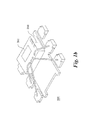
- FIG. 1a shows a perspective view of an exemplary embodiment of a gas sensor integrated onto a semiconductor circuit including a molding compound.
- FIG. 1a shows a gas sensor 100 which includes an ASIC (application specific integrated circuit) 200, a parallel plate capacitive sensor 300 on the ASIC 200, and a molding compound 400 over the gas sensor 100.
- the molding compound 400 includes an opening 410, which exposes the capacitive sensor 300 to the ambient environment so that it may make a reading of the condition it is designed to sense.
- FIG. 1b shows an isometric view of the sensor 100 of FIG. 1a without the molding compound 400.
- the sensor 300 is shown roughly centered on top of the ASIC 200 to illustrate one embodiment of the device.
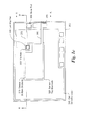
- FIG.1c shows a perspective view of an exemplary embodiment of the ASIC 200 with a sensor 300 integrated onto it.
- the molding compound 400 is not shown for clarity.
- the bottom electrode 310 may be formed using high precision semiconductor lithographic processes and in an embodiment may be comprised of a thin metal layer.
- the bottom electrode may be formed of Au with a TiW adhesion/barrier layer.
- the bottom electrode may be located above the active circuitry of the semiconductor circuit or ASIC, which results in a more compact design than sensors with interdigitated electrodes which are not placed atop active circuitry.
- the porous top electrode 320 fully overlays the bottom electrode.
- overlay is used herein in the sense that the footprint or area of the top electrode fully overlaps the footprint of the bottom electrode forming essentially a parallel plate capacitor, but does imply contact between the top and bottom electrodes.
- the top electrode is a porous electrode.
- porous is used herein the sense of not being totally impervious to the gases of interest. Examples of porous electrodes useful for carrying out embodiments of the present invention include but are not limited to film based porous electrodes, organic binders filled with platinum or carbon particles, and the like, by way of non-limiting example only.
- the top electrode 320 is fabricated using a process to provide favorable porosity and adhesion, this process being generally less dimensionally accurate than those used to photolithographically image metal electrodes on semiconductor wafers as in the bottom electrode.
- the baseline capacitance of the capacitive sensor is determined by the overlay of the bottom and top electrodes.
- the capacitance may be between about 1.5 pF and about 10 pF capacitance, however, this is exemplary only and various other ranges may be used (e.g. a range of about 0.2 pF to about 20 pF) depending on the requirements of the particular application.
- the top electrode 320 may have a surface area larger than the surface area of the bottom electrode 310 as shown in FIG. 1c . In this way, complete overlay of the top electrode over the bottom electrode may be ensured and as a result the capacitance of the sensor will be consistent even if there is misalignment of the top electrode. The capacitance will be consistent as long as the misalignment does not cause the top electrode to no longer fully cover the bottom electrode.
- FIG. 1c also shows bond pads 360 and 380 and metal traces 370 and 390.
- bond pad 360 is electrically connected to the landing pad (which is connected to the top electrode) by metal trace 370.
- bond pad 380 is electrically connected to the bottom electrode by metal trace 390.
- a metal bottom layer is formed on the passivation layer of the ASIC, it is formed so that the electrode portion of the bottom layer makes contact with metal trace 380 and the landing pad portion of the bottom layer makes contact with metal trace 360.
- the bond pads are features that are designed as part of the ASIC so that a gas sensor can later be fabricated onto the ASIC.
- bond pads 360 and 380 are electrically connected to the circuitry of the ASIC that determines the condition (such as a gas) being sensed.
- the ASIC or semiconductor circuit may also include output leads (not shown) that provide a signal with data indicative of the detected concentration of gas.
- the semiconductor circuit measures the capacitance of the gas sensitive layer by applying a signal to the metal bottom electrode (310) and measuring the charge displaced by the capacitor through the top electrode. The measurement is then used by the ASIC or semiconductor circuit to determine the condition being sensed.
- FIG. 2 shows a partial cross sectional view A-A of the width of the shorter side of ASIC 200 of FIG.1c .
- the top electrode 320 completely covers and overlays the bottom electrode 310 and makes connection to landing pad 330 for electrical interconnection of the top electrode 320 to the semiconductor circuitry.
- the gas sensing material layer 340 has defined therein an opening or via 350 filled with conductive material through which electrical contact is made between the top electrode 320 and the landing pad 330.
- the top electrode deposition process should ensure the top electrode 320 makes a reliable electrical interconnection to the landing pad 330 through the via 350.
- the gas sensing material 340 may be a dielectric material.
- the dielectric material may be a polymeric material such as a polymer film having a thickness of about 2 micrometers (microns).
- a polyimide organic polymer
- gas sensitive polymer materials are known in the art and thus a further description is omitted herein for the sake of brevity.
- FIG. 3 shows a cross sectional lengthwise view B-B of the longer side of ASIC 200 of FIG. 1c .
- This view shows the overlap of the packaging molding compound 400 over bond pads 360 and 380 used to interconnect the top 320 and bottom 310 electrodes to the ASIC circuitry, respectively.
- the molding compound 400 covers the capacitor interconnection pads by at least 0.1 mm in order to ensure that small changes in the molding compound caused by the gas of interest being measured do not affect the dielectric coupling between the sensing capacitor connection traces or connection pads.
- FIG. 4 shows a partial cross sectional view A-A of the width of the ASIC 200 of FIG.1c .
- FIG. 4 is similar to FIG. 2 except that it also shows how traces in the active circuitry underneath the semiconductor passivation layer can capacitively couple to the bottom electrode.
- the capacitive coupling is represented by the capacitor symbols 220 shown in the ASIC 200 that connect to ASIC circuitry 230.
- the sensor on the ASIC is a capacitive humidity sensor.
- the placement of a capacitive gas sensor directly atop active circuitry creates unintended parasitic capacitive coupling from the underlying circuitry to the bottom electrode of the capacitor as shown in FIG. 4 .
- the accuracy of the sensor charge displacement measurement can be affected by this additional parasitic capacitive coupling.
- the coupling may not be predictable or easily modeled using traditional circuitry modeling tools, as the circuitry beneath the bottom electrode is not in any way constrained by the presence of the gas sensing capacitor.
- the bottom electrode is driven by a low impedance voltage of known level, and the charge displaced by the sensing capacitor (a portion of which is due to the gas concentration) as a result of this applied voltage is measured using the top electrode.
- the voltage on the bottom electrode of the sensing capacitor, and therefore the charge displaced from the sensing capacitor, are unaffected by the parasitic capacitive coupling to any circuitry below the semiconductor passivation surface.
- the semiconductor circuitry in the exemplary embodiment is produced using standard and highly cost effective CMOS design and fabrication ground rules and can be built on the largest wafers appropriate for the application (200mm or 300mm diameter silicon wafers, for example). This fabrication processing produces wafers that have exposed electrical interconnection bonding and testing pads, with the majority of the exposed top surface and all interconnection circuitry covered in a silicon nitride or silicon dioxide or similar passivation layer. In the current invention it is intended that the capacitive gas sensor be built directly atop this external passivation layer.
- the steps in the fabrication of the capacitor and associated traces and packaging material according to an aspect of the present invention are conducted at sufficiently low temperatures to avoid damaging, or otherwise deleteriously affecting the performance or reliability of the underlying active semiconductor circuitry.
- the bottom electrode and the landing pad for the top electrode are fabricated using standard, low risk, low cost photolithographic processes such as PVD sputtering or evaporation, photolithographic resist imaging including develop and strip, and wet etching.
- the gas sensitive material and the porous top electrode do not damage materials typically exposed on the surface of a wafer at the conclusion of standard CMOS processing, including silicon nitride, silicon dioxide, aluminum, or silicon itself.
- the gas sensitive layer can be deposited using typical wafer processing techniques such as spin coating and baking, and the material may be patterned using photolithographic techniques similar to those use in the processing or semiconductor polymers (including photoresists and polyimides).
- the porous top electrode material may be deposited using a number of low temperature techniques including stencil printing, pad printing, ink jetting, or spin coating. The curing or baking temperatures required in all post CMOS processes are kept below temperatures which would cause harm to the underlying circuitry.
- a semiconductor circuit (such as an ASIC) having an integrated gas sensor may be constructed using a method that uses low temperatures that prevent damage to the semiconductor circuit.
- FIG. 5 in conjunction with Figures 2 and 3 , there is shown a simplified logic flow chart or diagram 500 illustrating processing steps according to aspects of the disclosure.
- a semiconductor circuit such as an ASIC is provided in block 510.
- the semiconductor circuit may include a passivation layer (210) on top, as well as exposed bond pads (360 and 380).
- a bottom electrode layer (310) and a landing pad (330) and metal traces (370 and 390) which are used to electrically connect the top (320) and bottom (310) electrodes of the gas sensor to the ASIC circuitry, are formed on the passivation layer (210).
- the gas sensitive layer (340) may be formed.
- the metal traces used to connect the bottom electrode and the landing pad to their respective bond pads are created from the same metal layer by selective patterning.
- the gas sensitive layer (340) may be a dielectric such as a polymer.
- a via or hole (350) is formed in the gas sensitive layer (340) using photolithographic patterning techniques.
- the top electrode layer (320) is formed onto the gas sensitive layer (340) using low temperature techniques such as screen printing, stencil printing, pad printing, ink jetting, or spin coating. Deposition of the top electrode layer creates an electrical contact through via 350 to the landing pad 330.
- the polymer material of the gas sensor may require curing, and as such the structure may be baked at an appropriate temperature for a given duration.
Landscapes
- Chemical & Material Sciences (AREA)
- Chemical Kinetics & Catalysis (AREA)
- Electrochemistry (AREA)
- Physics & Mathematics (AREA)
- Health & Medical Sciences (AREA)
- Life Sciences & Earth Sciences (AREA)
- Analytical Chemistry (AREA)
- Biochemistry (AREA)
- General Health & Medical Sciences (AREA)
- General Physics & Mathematics (AREA)
- Immunology (AREA)
- Pathology (AREA)
- Engineering & Computer Science (AREA)
- Power Engineering (AREA)
- Investigating Or Analyzing Materials By The Use Of Electric Means (AREA)
Abstract
Description
- The present invention relates generally to capacitive gas sensors constructed directly on top of the outermost passivation layer of a semiconductor circuit.
- Capacitive gas sensors are known in the art, a particular example being in the measurement of water vapor (relative humidity). There are a number of configurations associated with these sensors. One configuration uses interdigitated coplanar electrodes of opposite polarity covered by a gas sensitive material in which increasing gas concentration causes an increase in the dielectric constant of such material thereby increasing the dielectric coupling between planar electrodes and thereby increasing the effective capacitance between the electrodes. In the case of the interdigitated electrodes, both electrodes are underneath the top surface of the gas sensitive material, and the dielectric coupling between the planar electrodes occurs by field fringing effects.
- Another configuration employs parallel plate-like electrodes with a layer of gas sensitive material between them such that changing gas concentration changes the dielectric constant of the gas sensitive material and changes the capacitance of the parallel plate capacitor. A parallel plate configuration described in
FR2750494 US 6,450,026 ) has a top electrode comprised of a highly porous conducting polymer that allows the diffusion of the selected gas through the electrode and into the gas sensitive material. This top electrode material is processed so that it is tightly bonded to the gas sensitive material and is chemically inert and environmentally robust.FR2750494 US 6,450,026 are incorporated by reference herein in their entirety. - The capacitance of a capacitive gas sensor is a function of gas concentration, and the capacitance is measured by associated electronics capable of exciting the sensor electrically. The cost of manufacture of the capacitive gas sensors is associated with the physical size of the sensor and the associated electronics, hence it is desirable to provide capacitive gas sensors as small as possible while still achieving desired accuracy and signal to noise ratio. As the size of gas sensitive capacitors is reduced, the gas sensitive capacitors become increasingly susceptible to signal degradation associated with stray capacitances, including parasitic capacitances found in interconnections and in the associated electronics. One way to reduce the effects of parasitic capacitances when using smaller capacitors is to locate the associated electronics as physically close to the sensor as possible.
- Along with reducing the size and therefore the cost of manufacture of the capacitive gas sensors, it is desirable to decrease the size and cost of the associated electronics. Reduced cost of manufacture of the associated electronics can be achieved through the use of application specific integrated circuits (ASICS) which provide all necessary functionality in a small low cost configuration.
- There are commercial devices available in which interdigitated coplanar capacitor electrodes are disposed on top of a section of an ASIC and a gas sensitive material layer is disposed on top of the coplanar sensor electrodes to form a gas sensor. This configuration for ASICs with interdigitated capacitor electrodes has a disadvantage in that if the interdigitated capacitor electrodes are directly over active circuitry in the ASIC, coupling and interference is likely. This results in a need for a larger silicon area to accommodate the sensor electrodes so they are not over active circuitry. Notably, the interdigitated electrodes cannot be shielded from the circuitry-induced stray coupling signals by the addition of a conductive layer intermediate the electrodes and underneath because such a conductive layer would significantly increase the baseline capacitive coupling between the interdigitated sensing electrodes. Since the signal generated by changing gas concentrations in the gas sensitive layer is measured as a changing percentage of capacitance, increasing the baseline capacitance will lower the sensitivity of the device. Another drawback to ASICs with interdigitated electrodes is the undesirable sensitivity of the inter electrode capacitance to foreign material on the top of the gas sensitive material layer. For example, water droplets or small metal particles on the surface of the gas sensitive material layer can significantly alter the dielectric coupling between the electrodes by distorting fringing electric fields generated by the electrodes.
- An alternative device has two separate chips: one chip has a gas sensing capacitor built atop an appropriate substrate and the second chip suitable circuitry. This two chip solution has the advantage of decoupling the production yields, the processes, and the substrate materials used to produce each part. However, these chips must be electrically interconnected using flip chip or wire bonding technology, both of which affect the behavior of the sensing capacitor. Further the cost of electrical and mechanical packaging is greater than the vertically integrated configuration.
- Therefore, there is a need for a smaller and more effective capacitive gas sensor constructed directly on top of an appropriate semiconductor circuitry.
- An embodiment of the present invention relates to a gas sensor assembly comprised of a parallel plate capacitive gas sensor which is constructed directly on top of the passivated surface of a standard semiconductor gas sensor ASIC. The configuration provides the benefits of the parallel plate sensor configuration while allowing the smallest possible sensor size.
- An object of the present invention is to produce a capacitive sensor for measuring gas atop a semiconductor circuit, whereby manufacture thereof is simplified.
- In addition to sensors to be used as gas sensors, the present invention relates to the manufacturing method for these sensors. In a preferred embodiment, this method relates to the successive stacking or formation of a thin metal layer, a gas sensitive layer, and a porous top electrode.
- A method for manufacturing a capacitive sensor on a passivation layer of a semiconductor circuit may comprise: the deposition of a metal layer atop the passivation layer covering the circuitry, the metallization layer patterned to create a bottom electrode, a first trace connecting the bottom electrode to a first bond pad, a landing pad, and a second trace connecting the landing pad to a second bond pad, the bottom electrode being positioned so that it is located over a portion of the semiconductor circuit which contains active circuitry; depositing a gas sensitive layer onto the bottom electrode and the landing pad; creating a via hole through the gas sensitive layer to expose the landing pad; and depositing a porous conductive electrode onto the gas sensitive layer to form a top electrode electrically connected to the landing pad through the via hole, wherein a portion of the top electrode completely overlays a surface area of the bottom electrode and the top electrode connects to the landing pad.
- In an embodiment, a method for manufacturing a capacitive sensor on a passivation layer of an ASIC (510) may comprise: forming a bottom electrode layer and landing pad (520) on a portion of the passivation layer located over active circuitry of the ASIC; forming a gas sensitive layer (530) onto the bottom electrode layer and the landing pad; creating a via hole (540) through the gas sensitive layer to the landing pad; forming a top electrode layer (550) onto the gas sensitive layer, wherein the top electrode layer completely overlays a surface area of the bottom electrode layer, and wherein the forming process for the top electrode layer includes filling the via hole with electrically conductive material, thereby forming an electrical connection between the top electrode layer and the landing pad.
- In an embodiment, the process used for forming the bottom electrode layer and landing pad from a metal layer deposited on the passivation layer may comprise a photolithographic process, a photolithographic resist process, or a wet etching process. A spin coating process may be used for forming a gas sensitive layer onto the bottom electrode layer and the landing pad. In an embodiment, the method may further comprise applying a pattern to the gas sensitive layer using a photolithographic technique followed by dry or wet etching processes. The process used for forming the porous top electrode layer onto the gas sensitive layer may comprise screen printing, stencil printing, pad printing, ink jetting, or spin coating. In an embodiment, the method may further comprise forming a molding compound onto the top electrode and the ASIC such that an opening in the molding compound exposes the top electrode to the ambient environment and such that the molding compound covers at least 0.1 mm of the gas sensitive material along all mold compound edges around the opening.
- A gas sensor may comprise: a semiconductor circuit (200) having a top passivation layer (210); a metal bottom electrode (310) on the passivation layer (210) of the semiconductor circuit (200), wherein the bottom electrode (310) is located over an area of the semiconductor circuit that contains active circuitry, a metal landing pad (330) on the passivation layer (210) and electrically separate from the bottom electrode (310); a gas sensitive layer (340) on the metal bottom electrode (310) and metal landing pad (330), the gas sensitive layer (340) having a via (350) defined therethrough; a porous top electrode (320) on the gas sensitive layer (340), wherein an area formed by the porous top electrode (320) completely overlays an area formed by the metal bottom electrode (310), and wherein the porous top electrode (320) is electrically connected to the landing pad (330) through the via (350) in the gas sensitive layer (340); and a first metal trace (390) connecting the metal bottom electrode (310) to a first bond pad (380) and a second metal trace (370) connecting the landing pad (330) to a second bond pad (360). The bottom electrode, landing pad and both connecting traces may be patterned from the same metal layer (for example, by selective patterning). In an embodiment, the semiconductor circuit measures the capacitance of the gas sensitive layer by applying a signal to the metal bottom electrode (310) and measuring the charge displaced by the capacitor through the top electrode.
- In an embodiment, the gas sensor layer (340) covers the first metal trace (390) and second metal trace (370), thereby preventing an electrical short circuit between the porous top electrode (320) and the metal bottom electrode (310) which may be caused by the process used to deposit the top electrode. In another embodiment, the gas sensor may further comprise a mold compound (400) adjacent the porous top electrode (320), the mold compound (400) having an opening (410) for exposing the porous top electrode (320) to the ambient environment, and wherein each side of the opening (410) in the mold compound overlays at least 0.1 mm of the gas sensitive layer (340). In the gas sensor, an area of the porous top electrode (320) may be larger than an area of the bottom electrode (310), thereby enabling the porous top electrode (320) to completely overlay the bottom electrode (310) even if they are misaligned.
-
FIG. 1a shows a perspective view of an exemplary embodiment of a capacitive sensor integrated onto a semiconductor circuit including an over-molding compound; -
FIG.1b shows a perspective view of an exemplary embodiment of a capacitive sensor integrated onto a semiconductor circuit, without an over-molding compound; -
FIG. 1c shows a top view of the exemplary embodiment of an ASIC with a capacitive sensor integrated onto it, including the alignment of the bottom electrode, landing pad, via hole, and the interconnection of the bottom electrode and landing pad to their respective bond pads; -
FIG. 2 shows a partial cross sectional view taken through A-A ofFIG. 1c of the width of the short side of the ASIC configuration ofFIG.1c , including the top electrode covering the bottom electrode and making contact through the via hole in the gas sensitive material layer; -
FIG. 3 shows a cross sectional lengthwise view taken through B-B ofFIG. 1c of the long side of the ASIC configuration ofFIG.1c , including the overlap of the die packaging material over the connection pads for the capacitor connections. -
FIG. 4 shows a partial cross sectional view taken through A-A ofFIG. 1c of the width of the short side of the ASIC configuration ofFIG.1c , including undesired parasitic capacitive coupling from the underlying circuitry to the bottom electrode; and -
FIG. 5 is a flowchart of a process for manufacturing semiconductor circuits with an integrated gas sensor according to an embodiment of the invention. - Reference will now be made in detail to the present exemplary embodiments of the invention, examples of which are illustrated in the accompanying drawings.
-
FIG. 1a shows a perspective view of an exemplary embodiment of a gas sensor integrated onto a semiconductor circuit including a molding compound. In particular,FIG. 1a shows agas sensor 100 which includes an ASIC (application specific integrated circuit) 200, a parallelplate capacitive sensor 300 on theASIC 200, and amolding compound 400 over thegas sensor 100. Themolding compound 400 includes anopening 410, which exposes thecapacitive sensor 300 to the ambient environment so that it may make a reading of the condition it is designed to sense. -
FIG. 1b shows an isometric view of thesensor 100 ofFIG. 1a without themolding compound 400. Thesensor 300 is shown roughly centered on top of theASIC 200 to illustrate one embodiment of the device. -
FIG.1c shows a perspective view of an exemplary embodiment of theASIC 200 with asensor 300 integrated onto it. Themolding compound 400 is not shown for clarity. Thebottom electrode 310 may be formed using high precision semiconductor lithographic processes and in an embodiment may be comprised of a thin metal layer. In one non-limiting embodiment, the bottom electrode may be formed of Au with a TiW adhesion/barrier layer. The bottom electrode may be located above the active circuitry of the semiconductor circuit or ASIC, which results in a more compact design than sensors with interdigitated electrodes which are not placed atop active circuitry. - The porous
top electrode 320 fully overlays the bottom electrode. The term overlay is used herein in the sense that the footprint or area of the top electrode fully overlaps the footprint of the bottom electrode forming essentially a parallel plate capacitor, but does imply contact between the top and bottom electrodes. In an embodiment, the top electrode is a porous electrode. The term "porous" is used herein the sense of not being totally impervious to the gases of interest. Examples of porous electrodes useful for carrying out embodiments of the present invention include but are not limited to film based porous electrodes, organic binders filled with platinum or carbon particles, and the like, by way of non-limiting example only. - The
top electrode 320 is fabricated using a process to provide favorable porosity and adhesion, this process being generally less dimensionally accurate than those used to photolithographically image metal electrodes on semiconductor wafers as in the bottom electrode. For given dielectric properties and thickness of the gas sensing material, the baseline capacitance of the capacitive sensor is determined by the overlay of the bottom and top electrodes. In one non-limiting embodiment, the capacitance may be between about 1.5 pF and about 10 pF capacitance, however, this is exemplary only and various other ranges may be used (e.g. a range of about 0.2 pF to about 20 pF) depending on the requirements of the particular application. To eliminate the unavoidable variance in capacitance that would result from using top and bottom electrodes of identical size and the positioning and geometric tolerances of the deposition processes, in an embodiment thetop electrode 320 may have a surface area larger than the surface area of thebottom electrode 310 as shown inFIG. 1c . In this way, complete overlay of the top electrode over the bottom electrode may be ensured and as a result the capacitance of the sensor will be consistent even if there is misalignment of the top electrode. The capacitance will be consistent as long as the misalignment does not cause the top electrode to no longer fully cover the bottom electrode. -
FIG. 1c also showsbond pads bond pad 360 is electrically connected to the landing pad (which is connected to the top electrode) bymetal trace 370. Similarly,bond pad 380 is electrically connected to the bottom electrode bymetal trace 390. When a metal bottom layer is formed on the passivation layer of the ASIC, it is formed so that the electrode portion of the bottom layer makes contact withmetal trace 380 and the landing pad portion of the bottom layer makes contact withmetal trace 360. As will be understood, the bond pads are features that are designed as part of the ASIC so that a gas sensor can later be fabricated onto the ASIC. As will further be understood,bond pads -
FIG. 2 shows a partial cross sectional view A-A of the width of the shorter side ofASIC 200 ofFIG.1c . In the embodiment ofFIG. 2 , thetop electrode 320 completely covers and overlays thebottom electrode 310 and makes connection tolanding pad 330 for electrical interconnection of thetop electrode 320 to the semiconductor circuitry. The gassensing material layer 340 has defined therein an opening or via 350 filled with conductive material through which electrical contact is made between thetop electrode 320 and thelanding pad 330. The top electrode deposition process should ensure thetop electrode 320 makes a reliable electrical interconnection to thelanding pad 330 through thevia 350. Thegas sensing material 340 may be a dielectric material. In one non-limiting embodiment, the dielectric material may be a polymeric material such as a polymer film having a thickness of about 2 micrometers (microns). By way of further non-limiting example, for the gas sensitive material layer a polyimide (organic polymer) may be used, as is well known and in commercial use for humidity sensing. Still further, it is understood that gas sensitive polymer materials are known in the art and thus a further description is omitted herein for the sake of brevity. -
FIG. 3 shows a cross sectional lengthwise view B-B of the longer side ofASIC 200 ofFIG. 1c . This view shows the overlap of thepackaging molding compound 400 overbond pads molding compound 400 covers the capacitor interconnection pads by at least 0.1 mm in order to ensure that small changes in the molding compound caused by the gas of interest being measured do not affect the dielectric coupling between the sensing capacitor connection traces or connection pads. -
FIG. 4 shows a partial cross sectional view A-A of the width of theASIC 200 ofFIG.1c .FIG. 4 is similar toFIG. 2 except that it also shows how traces in the active circuitry underneath the semiconductor passivation layer can capacitively couple to the bottom electrode. The capacitive coupling is represented by thecapacitor symbols 220 shown in theASIC 200 that connect toASIC circuitry 230. - In an embodiment, the sensor on the ASIC is a capacitive humidity sensor. The placement of a capacitive gas sensor directly atop active circuitry creates unintended parasitic capacitive coupling from the underlying circuitry to the bottom electrode of the capacitor as shown in
FIG. 4 . Because the change in capacitance with gas concentration is small relative to capacitance of the gas sensitive material at zero concentration, the accuracy of the sensor charge displacement measurement can be affected by this additional parasitic capacitive coupling. Further, the coupling may not be predictable or easily modeled using traditional circuitry modeling tools, as the circuitry beneath the bottom electrode is not in any way constrained by the presence of the gas sensing capacitor. In order to avoid the deleterious effects of these parasitic connections, in embodiments of the current invention the bottom electrode is driven by a low impedance voltage of known level, and the charge displaced by the sensing capacitor (a portion of which is due to the gas concentration) as a result of this applied voltage is measured using the top electrode. The voltage on the bottom electrode of the sensing capacitor, and therefore the charge displaced from the sensing capacitor, are unaffected by the parasitic capacitive coupling to any circuitry below the semiconductor passivation surface. - In order to reduce the cost and increase the reliability of the resulting sensor assembly, it is important that the processing associated with the gas sensing capacitor and its insulation and interconnection not damage the underlying circuitry. The semiconductor circuitry in the exemplary embodiment is produced using standard and highly cost effective CMOS design and fabrication ground rules and can be built on the largest wafers appropriate for the application (200mm or 300mm diameter silicon wafers, for example). This fabrication processing produces wafers that have exposed electrical interconnection bonding and testing pads, with the majority of the exposed top surface and all interconnection circuitry covered in a silicon nitride or silicon dioxide or similar passivation layer. In the current invention it is intended that the capacitive gas sensor be built directly atop this external passivation layer.
- The steps in the fabrication of the capacitor and associated traces and packaging material according to an aspect of the present invention are conducted at sufficiently low temperatures to avoid damaging, or otherwise deleteriously affecting the performance or reliability of the underlying active semiconductor circuitry. The bottom electrode and the landing pad for the top electrode are fabricated using standard, low risk, low cost photolithographic processes such as PVD sputtering or evaporation, photolithographic resist imaging including develop and strip, and wet etching. The gas sensitive material and the porous top electrode do not damage materials typically exposed on the surface of a wafer at the conclusion of standard CMOS processing, including silicon nitride, silicon dioxide, aluminum, or silicon itself. The gas sensitive layer can be deposited using typical wafer processing techniques such as spin coating and baking, and the material may be patterned using photolithographic techniques similar to those use in the processing or semiconductor polymers (including photoresists and polyimides). The porous top electrode material may be deposited using a number of low temperature techniques including stencil printing, pad printing, ink jetting, or spin coating. The curing or baking temperatures required in all post CMOS processes are kept below temperatures which would cause harm to the underlying circuitry.
- In an embodiment, a semiconductor circuit (such as an ASIC) having an integrated gas sensor may be constructed using a method that uses low temperatures that prevent damage to the semiconductor circuit. Referring now to
FIG. 5 , in conjunction withFigures 2 and3 , there is shown a simplified logic flow chart or diagram 500 illustrating processing steps according to aspects of the disclosure. A semiconductor circuit such as an ASIC is provided inblock 510. The semiconductor circuit may include a passivation layer (210) on top, as well as exposed bond pads (360 and 380). Atblock 520, a bottom electrode layer (310) and a landing pad (330) and metal traces (370 and 390) which are used to electrically connect the top (320) and bottom (310) electrodes of the gas sensor to the ASIC circuitry, are formed on the passivation layer (210). Atblock 530, the gas sensitive layer (340) may be formed. In one configuration, the metal traces used to connect the bottom electrode and the landing pad to their respective bond pads are created from the same metal layer by selective patterning. The gas sensitive layer (340) may be a dielectric such as a polymer. Atblock 540, a via or hole (350) is formed in the gas sensitive layer (340) using photolithographic patterning techniques. Atblock 550, the top electrode layer (320) is formed onto the gas sensitive layer (340) using low temperature techniques such as screen printing, stencil printing, pad printing, ink jetting, or spin coating. Deposition of the top electrode layer creates an electrical contact through via 350 to thelanding pad 330. In one non-limiting example, the polymer material of the gas sensor may require curing, and as such the structure may be baked at an appropriate temperature for a given duration. - While the foregoing describes exemplary embodiments and implementations, it will be apparent to those skilled in the art that various modifications and variations can be made to the present invention without departing from the spirit and scope of the invention.
Claims (10)
- A method for manufacturing a capacitive sensor on a passivation layer of a semiconductor circuit, the passivation layer having openings which expose a first bond pad (360) and a second bond pad (380) comprising:forming a metal layer onto the passivation layer (520) and patterning the metal layer to form a bottom electrode and landing pad and metal traces connecting the bottom electrode and the landing pad to their respective bond pads, the bottom electrode being positioned so that it is located over a portion of the semiconductor circuit with active circuitry;forming a gas sensitive layer onto the bottom electrode and the landing pad (530);creating a via (540) through the gas sensitive layer to the landing pad;forming a porous electrode onto the gas sensitive layer (550) electrically connected to the landing pad through the via hole, wherein a portion of the top electrode completely overlays the surface area of the bottom electrode and an other portion of the top electrode is in contact with the landing pad.
- The method of claim 1, further comprising forming a molding compound onto the top electrode and the ASIC such that an opening in the molding compound exposes the top electrode to an ambient environment and such that the molding compound covers at least 0.1 mm of the gas sensitive layer along all mold compound edges around the opening.
- A method for manufacturing a capacitive sensor on a passivation layer of an ASIC comprising:forming a bottom electrode layer and landing pad (520) on a portion of the passivation layer located over active circuitry of the ASIC using a low temperature process;forming a gas sensitive layer (530) onto the bottom electrode layer and the landing pad;creating a via (540) through the gas sensitive layer to the landing pad;forming a top electrode layer (550) onto the gas sensitive layer using a low temperature process, wherein the top electrode layer completely overlays a surface area of the bottom electrode layer, and wherein the forming the top electrode layer deposits a portion of the top electrode layer into the via, thereby forming an electrical connection between the top electrode layer and the landing pad;
- The method of claim 3, further comprising forming a molding compound onto the top electrode layer and the ASIC such that an opening in the molding compound exposes the top electrode layer to the ambient environment and such that the molding compound covers at least 0.1 mm of the gas sensitive layer along all mold compound edges around the opening.
- A gas sensor comprising:a semiconductor circuit (200) having a top passivation layer (210);a metal bottom electrode (310) on the passivation layer (210) of the semiconductor circuit (200), wherein said metal bottom electrode (310) is located over an area of the semiconductor circuit that contains active circuitry,a metal landing pad (330) on the passivation layer (210) and electrically separate from the metal bottom electrode (310);a gas sensitive layer (340) on the metal bottom electrode (310) and the metal landing pad (330), the gas sensitive layer (340) including a via hole (350) exposing a portion of the landing pad;a porous top electrode (320) on the gas sensitive layer (340), wherein an area formed by the porous top electrode (320) completely overlays an area formed by the metal bottom electrode (310), and wherein the porous top electrode (320) is electrically connected to the landing pad (330) through the via hole (350) in the gas sensitive layer (340); anda first metal trace (390) between the metal bottom electrode (310) and a first bond pad (380) and a second metal trace (370) between the landing pad (330) and a second bond pad (360);wherein the semiconductor circuit measures a capacitance of the gas sensitive layer by applying a signal to the metal bottom electrode (310) and measuring a charge displaced by the capacitance through the porous top electrode.
- The gas sensor of claim 5, wherein the gas sensitive layer (340) covers the first metal trace (390) and the second metal trace (370), thereby preventing an electrical short circuit between the porous top electrode (320) and the metal bottom electrode (310).
- The gas sensor of claim 5, further comprising a mold compound (400) adjacent the porous top electrode (320), the mold compound (400) having an opening (410) for exposing the porous top electrode (320) to an ambient environment, and wherein each side of the opening (410) in the mold compound overlays at least 0.1 mm of the gas sensitive layer (340).
- The gas sensor of claim 5, wherein an area of the porous top electrode (320) is larger than an area of the metal bottom electrode (310), thereby enabling the porous top electrode (320) to completely overlay the bottom electrode (310) even if they are misaligned.
- A gas sensor comprising:a semiconductor circuit capable of measuring the capacitance of the parallel plate capacitive sensor by applying a voltage and measuring the resultant displaced charge;a metal layer formed directly onto the outer surface of a passivation layer of the semiconductor circuit and located over surface area of the semiconductor circuit that contains active circuitry, wherein the metal layer forms the bottom electrode of the capacitive gas sensor, a landing pad for the connection of the top porous electrode of the capacitive gas sensor, and traces connecting both the bottom electrode and the landing pad to separate bond pads which are connected to the semiconductor circuitry and which were formed as a part of the ASIC fabrication process of the semiconductor circuit;a gas sensitive material layer deposited onto the passivation on the outer surface of the semiconductor circuit covering the metal layer, the gas sensitive layer patterned to define a via hole for electrically connecting a porous top electrode to the landing pad and to expose the bonding pads of the semiconductor circuit;a porous top electrode deposited onto the sensitive layer so as to completely cover the bottom electrode pattern formed in the metal layer and to make electrical connection to the landing pad;wherein the semiconductor circuit measures the capacitance of the gas sensitive layer by applying a signal to the bottom electrode and measuring the charge displaced by the capacitor through the top electrode.
- The sensor configuration of claim 9, wherein the gas sensitive layer is configured to cover the metal trace connecting the bottom electrode to its bond pad and the metal trace connecting the top electrode landing pad to its bond pad over an area exceeding the maximum area of the top electrode, thus preventing an electrical short circuit between the porous top electrode and the bottom electrode.
Priority Applications (6)
| Application Number | Priority Date | Filing Date | Title |
|---|---|---|---|
| EP13305026.0A EP2755023B1 (en) | 2013-01-11 | 2013-01-11 | Capacitive sensor integrated onto semiconductor circuit |
| KR1020157021732A KR101970229B1 (en) | 2013-01-11 | 2014-01-06 | Capacitive sensor integrated onto semiconductor circuit |
| JP2015552036A JP6129341B2 (en) | 2013-01-11 | 2014-01-06 | Capacitance sensor integrated on a semiconductor circuit |
| CN201480004701.0A CN105264365B (en) | 2013-01-11 | 2014-01-06 | It is integrated into the capacitive sensor and its manufacturing method of semi-conductor electricity road |
| PCT/EP2014/050097 WO2014108371A1 (en) | 2013-01-11 | 2014-01-06 | Capacitive sensor integrated onto semiconductor circuit |
| US14/152,085 US9239310B2 (en) | 2013-01-11 | 2014-01-10 | Capacitive sensor integrated onto semiconductor circuit |
Applications Claiming Priority (1)
| Application Number | Priority Date | Filing Date | Title |
|---|---|---|---|
| EP13305026.0A EP2755023B1 (en) | 2013-01-11 | 2013-01-11 | Capacitive sensor integrated onto semiconductor circuit |
Publications (2)
| Publication Number | Publication Date |
|---|---|
| EP2755023A1 true EP2755023A1 (en) | 2014-07-16 |
| EP2755023B1 EP2755023B1 (en) | 2017-06-21 |
Family
ID=47632946
Family Applications (1)
| Application Number | Title | Priority Date | Filing Date |
|---|---|---|---|
| EP13305026.0A Active EP2755023B1 (en) | 2013-01-11 | 2013-01-11 | Capacitive sensor integrated onto semiconductor circuit |
Country Status (6)
| Country | Link |
|---|---|
| US (1) | US9239310B2 (en) |
| EP (1) | EP2755023B1 (en) |
| JP (1) | JP6129341B2 (en) |
| KR (1) | KR101970229B1 (en) |
| CN (1) | CN105264365B (en) |
| WO (1) | WO2014108371A1 (en) |
Cited By (4)
| Publication number | Priority date | Publication date | Assignee | Title |
|---|---|---|---|---|
| WO2017049203A1 (en) * | 2015-09-16 | 2017-03-23 | Systems And Software Enterprises, Llc | Enhanced liquid detection mechanisms for circuit cards |
| EP3364181A1 (en) | 2017-02-21 | 2018-08-22 | E+E Elektronik Ges.M.B.H. | Moisture sensor assembly |
| EP3714772A1 (en) * | 2019-03-29 | 2020-09-30 | Picosun Oy | Sensor and its manufacturing method |
| EP4215908A1 (en) | 2022-01-19 | 2023-07-26 | E+E Elektronik Ges.M.B.H. | Moisture sensor assembly |
Families Citing this family (21)
| Publication number | Priority date | Publication date | Assignee | Title |
|---|---|---|---|---|
| US9618653B2 (en) * | 2013-03-29 | 2017-04-11 | Stmicroelectronics Pte Ltd. | Microelectronic environmental sensing module |
| US9176089B2 (en) | 2013-03-29 | 2015-11-03 | Stmicroelectronics Pte Ltd. | Integrated multi-sensor module |
| US9000542B2 (en) | 2013-05-31 | 2015-04-07 | Stmicroelectronics Pte Ltd. | Suspended membrane device |
| US10042488B2 (en) * | 2014-04-04 | 2018-08-07 | Synaptics Incorporated | Through silicon vias for backside connection |
| CN104391008B (en) * | 2014-11-14 | 2017-06-16 | 无锡信大气象传感网科技有限公司 | A kind of manufacture method of sensor element |
| KR102376065B1 (en) | 2015-10-12 | 2022-03-18 | 현대모비스 주식회사 | Motor driven power steering system control method |
| KR102307258B1 (en) * | 2015-11-20 | 2021-10-01 | 현대모비스 주식회사 | Steering return control apparatus of motor driven power steering and method thereof |
| US10336606B2 (en) | 2016-02-25 | 2019-07-02 | Nxp Usa, Inc. | Integrated capacitive humidity sensor |
| US10254261B2 (en) | 2016-07-18 | 2019-04-09 | Stmicroelectronics Pte Ltd | Integrated air quality sensor that detects multiple gas species |
| US10429330B2 (en) | 2016-07-18 | 2019-10-01 | Stmicroelectronics Pte Ltd | Gas analyzer that detects gases, humidity, and temperature |
| US10996183B2 (en) | 2016-07-22 | 2021-05-04 | Sharp Kabushiki Kaisha | Detection device and method of controlling detection device |
| US11287395B2 (en) | 2016-09-09 | 2022-03-29 | Hokuriku Electric Industry Co., Ltd. | Capacitive gas sensor |
| US10557812B2 (en) | 2016-12-01 | 2020-02-11 | Stmicroelectronics Pte Ltd | Gas sensors |
| JP6829181B2 (en) * | 2017-11-28 | 2021-02-10 | 株式会社東芝 | Gas sensor |
| CN107960008B (en) * | 2017-12-25 | 2020-06-12 | 浙江常山聚华电子有限公司 | Integrated circuit board |
| CN108195898B (en) * | 2017-12-25 | 2020-08-04 | 佛山市领能电子科技有限公司 | Gas sensing and capacitor composite circuit board |
| CN108088877B (en) * | 2017-12-25 | 2020-05-01 | 江西省吉晶微电子有限公司 | Multifunctional semiconductor device |
| EP3598118A1 (en) | 2018-07-20 | 2020-01-22 | MEAS France | Capacitive gas sensors and manufacturing method thereof |
| CN110346423B (en) * | 2019-07-02 | 2021-05-04 | 杭州未名信科科技有限公司 | CMOS-MEMS humidity sensor |
| EP3845895A1 (en) | 2020-01-02 | 2021-07-07 | MEAS France | Multi-sensing capacitive sensors |
| CN111289584B (en) * | 2020-04-03 | 2023-06-02 | 上海集成电路研发中心有限公司 | Capacitive gas sensor and preparation method thereof |
Citations (5)
| Publication number | Priority date | Publication date | Assignee | Title |
|---|---|---|---|---|
| FR2750494A1 (en) | 1996-07-01 | 1998-01-02 | S P S I Soc | High sensitivity capacitive humidity sensor |
| US6450026B1 (en) | 1997-12-31 | 2002-09-17 | Jean Desarnaud | Capacitive sensors for measuring humidity and method of making same |
| US20040008471A1 (en) * | 2002-07-09 | 2004-01-15 | Davis Richard A. | Relative humidity sensor with integrated signal conditioning |
| US20070264741A1 (en) * | 2002-09-13 | 2007-11-15 | Xsilogy, Inc. | Methods for making fixed parallel plate MEMS capacitor microsensors and microsensor arrays |
| EP2420826A1 (en) * | 2010-08-17 | 2012-02-22 | Nxp B.V. | Integrated Circuit and Manufacturing Method Therefor |
Family Cites Families (6)
| Publication number | Priority date | Publication date | Assignee | Title |
|---|---|---|---|---|
| US4603372A (en) * | 1984-11-05 | 1986-07-29 | Direction De La Meteorologie Du Ministere Des Transports | Method of fabricating a temperature or humidity sensor of the thin film type, and sensors obtained thereby |
| JPH0269624A (en) * | 1988-09-05 | 1990-03-08 | Matsushita Electric Ind Co Ltd | Pyroelectric infrared ray detecting element |
| JP3030944B2 (en) * | 1991-07-03 | 2000-04-10 | ソニー株式会社 | Multi-plate color camera |
| JPH0514909U (en) * | 1991-07-30 | 1993-02-26 | 三菱重工業株式会社 | Capacitance type humidity sensor |
| JP2006019589A (en) * | 2004-07-02 | 2006-01-19 | Denso Corp | Semiconductor apparatus |
| US20120167392A1 (en) * | 2010-12-30 | 2012-07-05 | Stmicroelectronics Pte. Ltd. | Razor with chemical and biological sensor |
-
2013
- 2013-01-11 EP EP13305026.0A patent/EP2755023B1/en active Active
-
2014
- 2014-01-06 CN CN201480004701.0A patent/CN105264365B/en active Active
- 2014-01-06 JP JP2015552036A patent/JP6129341B2/en active Active
- 2014-01-06 KR KR1020157021732A patent/KR101970229B1/en active IP Right Grant
- 2014-01-06 WO PCT/EP2014/050097 patent/WO2014108371A1/en active Application Filing
- 2014-01-10 US US14/152,085 patent/US9239310B2/en active Active
Patent Citations (5)
| Publication number | Priority date | Publication date | Assignee | Title |
|---|---|---|---|---|
| FR2750494A1 (en) | 1996-07-01 | 1998-01-02 | S P S I Soc | High sensitivity capacitive humidity sensor |
| US6450026B1 (en) | 1997-12-31 | 2002-09-17 | Jean Desarnaud | Capacitive sensors for measuring humidity and method of making same |
| US20040008471A1 (en) * | 2002-07-09 | 2004-01-15 | Davis Richard A. | Relative humidity sensor with integrated signal conditioning |
| US20070264741A1 (en) * | 2002-09-13 | 2007-11-15 | Xsilogy, Inc. | Methods for making fixed parallel plate MEMS capacitor microsensors and microsensor arrays |
| EP2420826A1 (en) * | 2010-08-17 | 2012-02-22 | Nxp B.V. | Integrated Circuit and Manufacturing Method Therefor |
Non-Patent Citations (3)
| Title |
|---|
| LAZARUS N ET AL: "Integrated vertical parallel-plate capacitive humidity sensor;Integrated vertical parallel-plate capacitive humidity sensor", JOURNAL OF MICROMECHANICS & MICROENGINEERING, INSTITUTE OF PHYSICS PUBLISHING, BRISTOL, GB, vol. 21, no. 6, 11 May 2011 (2011-05-11), pages 65028, XP020205572, ISSN: 0960-1317, DOI: 10.1088/0960-1317/21/6/065028 * |
| PLUM T J ET AL: "Design of a MEMS capacitive chemical sensor based on polymer swelling", MICROELECTRONICS AND ELECTRON DEVICES, 2006. WMED '06. 2006 IEEE WORKS HOP ON BOISE, ID, USA APRIL 14, 2006, PISCATAWAY, NJ, USA,IEEE, 14 April 2006 (2006-04-14), pages 49 - 50, XP010935613, ISBN: 978-1-4244-0374-5, DOI: 10.1109/WMED.2006.1678304 * |
| RALPH FENNER ET AL: "Micromachined Water Vapor Sensors: A Review of Sensing Technologies", IEEE SENSORS JOURNAL, IEEE SERVICE CENTER, NEW YORK, NY, US, vol. 1, no. 4, 1 December 2001 (2001-12-01), XP011055588, ISSN: 1530-437X * |
Cited By (8)
| Publication number | Priority date | Publication date | Assignee | Title |
|---|---|---|---|---|
| WO2017049203A1 (en) * | 2015-09-16 | 2017-03-23 | Systems And Software Enterprises, Llc | Enhanced liquid detection mechanisms for circuit cards |
| US10090669B2 (en) | 2015-09-16 | 2018-10-02 | Systems And Software Enterprises, Llc | Enhanced liquid detection mechanisms for circuit cards |
| EP3364181A1 (en) | 2017-02-21 | 2018-08-22 | E+E Elektronik Ges.M.B.H. | Moisture sensor assembly |
| WO2018153532A1 (en) | 2017-02-21 | 2018-08-30 | E+E Elektronik Ges.M.B.H | Humidity sensor arrangement |
| CN110312930A (en) * | 2017-02-21 | 2019-10-08 | 益加义电子有限公司 | Humidity sensor apparatus |
| EP3714772A1 (en) * | 2019-03-29 | 2020-09-30 | Picosun Oy | Sensor and its manufacturing method |
| EP4215908A1 (en) | 2022-01-19 | 2023-07-26 | E+E Elektronik Ges.M.B.H. | Moisture sensor assembly |
| WO2023138955A1 (en) | 2022-01-19 | 2023-07-27 | E+E Elektronik Ges.M.B.H | Humidity sensor arrangement |
Also Published As
| Publication number | Publication date |
|---|---|
| JP2016504595A (en) | 2016-02-12 |
| CN105264365B (en) | 2018-08-21 |
| WO2014108371A1 (en) | 2014-07-17 |
| KR101970229B1 (en) | 2019-04-18 |
| CN105264365A (en) | 2016-01-20 |
| US9239310B2 (en) | 2016-01-19 |
| JP6129341B2 (en) | 2017-05-17 |
| US20140197500A1 (en) | 2014-07-17 |
| EP2755023B1 (en) | 2017-06-21 |
| KR20150141932A (en) | 2015-12-21 |
Similar Documents
| Publication | Publication Date | Title |
|---|---|---|
| EP2755023B1 (en) | Capacitive sensor integrated onto semiconductor circuit | |
| US10317357B2 (en) | Integrated multi-sensor module | |
| EP2492239B1 (en) | Integrated circuit with sensor and method of manufacturing such an integrated circuit | |
| US9239309B2 (en) | Humidity sensor and method of manufacturing the same | |
| EP2481703A1 (en) | Sensor protection | |
| US8188555B2 (en) | Capacitive sensor and manufacturing method therefor | |
| JP4674529B2 (en) | Humidity sensor device and manufacturing method thereof | |
| JP5516505B2 (en) | Capacitive humidity sensor and manufacturing method thereof | |
| JP2003004683A (en) | Capacitance-type humidity sensor | |
| EP3206027B1 (en) | Sensor chip comprising electrostatic discharge protection element | |
| KR20160045678A (en) | Connection pads for a fingerprint sensing device | |
| EP3001186B1 (en) | Sensor chip | |
| JP5470512B2 (en) | Humidity detection sensor | |
| US9234859B2 (en) | Integrated device of a capacitive type for detecting humidity, in particular manufactured using a CMOS technology | |
| US11428661B2 (en) | Method for producing a moisture sensor at the wafer level and moisture sensor | |
| CN110088037B (en) | Semiconductor device and method for forming semiconductor device | |
| US9766195B2 (en) | Integrated circuit with sensor and method of manufacturing such an integrated circuit | |
| US11674916B2 (en) | Gas sensor | |
| EP2482310A1 (en) | Through vias in a sensor chip | |
| WO2019131564A1 (en) | Measurement instrument for chemical/physical phenomena and method for manufacturing same | |
| US20220252534A1 (en) | Method of forming a sensor device | |
| JP2006082280A (en) | Screen printing method | |
| CN111310687A (en) | Low-cost non-excitation signal fingerprint acquisition unit | |
| JP2013044552A (en) | Wafer inspection method and wafer map |
Legal Events
| Date | Code | Title | Description |
|---|---|---|---|
| PUAI | Public reference made under article 153(3) epc to a published international application that has entered the european phase |
Free format text: ORIGINAL CODE: 0009012 |
|
| 17P | Request for examination filed |
Effective date: 20130111 |
|
| AK | Designated contracting states |
Kind code of ref document: A1 Designated state(s): AL AT BE BG CH CY CZ DE DK EE ES FI FR GB GR HR HU IE IS IT LI LT LU LV MC MK MT NL NO PL PT RO RS SE SI SK SM TR |
|
| AX | Request for extension of the european patent |
Extension state: BA ME |
|
| R17P | Request for examination filed (corrected) |
Effective date: 20141211 |
|
| RBV | Designated contracting states (corrected) |
Designated state(s): AL AT BE BG CH CY CZ DE DK EE ES FI FR GB GR HR HU IE IS IT LI LT LU LV MC MK MT NL NO PL PT RO RS SE SI SK SM TR |
|
| GRAP | Despatch of communication of intention to grant a patent |
Free format text: ORIGINAL CODE: EPIDOSNIGR1 |
|
| INTG | Intention to grant announced |
Effective date: 20170125 |
|
| GRAS | Grant fee paid |
Free format text: ORIGINAL CODE: EPIDOSNIGR3 |
|
| GRAA | (expected) grant |
Free format text: ORIGINAL CODE: 0009210 |
|
| AK | Designated contracting states |
Kind code of ref document: B1 Designated state(s): AL AT BE BG CH CY CZ DE DK EE ES FI FR GB GR HR HU IE IS IT LI LT LU LV MC MK MT NL NO PL PT RO RS SE SI SK SM TR |
|
| REG | Reference to a national code |
Ref country code: GB Ref legal event code: FG4D |
|
| REG | Reference to a national code |
Ref country code: CH Ref legal event code: EP |
|
| REG | Reference to a national code |
Ref country code: IE Ref legal event code: FG4D |
|
| REG | Reference to a national code |
Ref country code: AT Ref legal event code: REF Ref document number: 903411 Country of ref document: AT Kind code of ref document: T Effective date: 20170715 |
|
| REG | Reference to a national code |
Ref country code: CH Ref legal event code: NV Representative=s name: MURGITROYD AND COMPANY, CH |
|
| REG | Reference to a national code |
Ref country code: DE Ref legal event code: R096 Ref document number: 602013022507 Country of ref document: DE |
|
| REG | Reference to a national code |
Ref country code: NL Ref legal event code: MP Effective date: 20170621 |
|
| PG25 | Lapsed in a contracting state [announced via postgrant information from national office to epo] |
Ref country code: FI Free format text: LAPSE BECAUSE OF FAILURE TO SUBMIT A TRANSLATION OF THE DESCRIPTION OR TO PAY THE FEE WITHIN THE PRESCRIBED TIME-LIMIT Effective date: 20170621 Ref country code: LT Free format text: LAPSE BECAUSE OF FAILURE TO SUBMIT A TRANSLATION OF THE DESCRIPTION OR TO PAY THE FEE WITHIN THE PRESCRIBED TIME-LIMIT Effective date: 20170621 Ref country code: NO Free format text: LAPSE BECAUSE OF FAILURE TO SUBMIT A TRANSLATION OF THE DESCRIPTION OR TO PAY THE FEE WITHIN THE PRESCRIBED TIME-LIMIT Effective date: 20170921 Ref country code: GR Free format text: LAPSE BECAUSE OF FAILURE TO SUBMIT A TRANSLATION OF THE DESCRIPTION OR TO PAY THE FEE WITHIN THE PRESCRIBED TIME-LIMIT Effective date: 20170922 Ref country code: HR Free format text: LAPSE BECAUSE OF FAILURE TO SUBMIT A TRANSLATION OF THE DESCRIPTION OR TO PAY THE FEE WITHIN THE PRESCRIBED TIME-LIMIT Effective date: 20170621 |
|
| REG | Reference to a national code |
Ref country code: LT Ref legal event code: MG4D |
|
| PG25 | Lapsed in a contracting state [announced via postgrant information from national office to epo] |
Ref country code: LV Free format text: LAPSE BECAUSE OF FAILURE TO SUBMIT A TRANSLATION OF THE DESCRIPTION OR TO PAY THE FEE WITHIN THE PRESCRIBED TIME-LIMIT Effective date: 20170621 Ref country code: RS Free format text: LAPSE BECAUSE OF FAILURE TO SUBMIT A TRANSLATION OF THE DESCRIPTION OR TO PAY THE FEE WITHIN THE PRESCRIBED TIME-LIMIT Effective date: 20170621 Ref country code: BG Free format text: LAPSE BECAUSE OF FAILURE TO SUBMIT A TRANSLATION OF THE DESCRIPTION OR TO PAY THE FEE WITHIN THE PRESCRIBED TIME-LIMIT Effective date: 20170921 Ref country code: SE Free format text: LAPSE BECAUSE OF FAILURE TO SUBMIT A TRANSLATION OF THE DESCRIPTION OR TO PAY THE FEE WITHIN THE PRESCRIBED TIME-LIMIT Effective date: 20170621 Ref country code: NL Free format text: LAPSE BECAUSE OF FAILURE TO SUBMIT A TRANSLATION OF THE DESCRIPTION OR TO PAY THE FEE WITHIN THE PRESCRIBED TIME-LIMIT Effective date: 20170621 |
|
| REG | Reference to a national code |
Ref country code: FR Ref legal event code: PLFP Year of fee payment: 6 |
|
| PG25 | Lapsed in a contracting state [announced via postgrant information from national office to epo] |
Ref country code: RO Free format text: LAPSE BECAUSE OF FAILURE TO SUBMIT A TRANSLATION OF THE DESCRIPTION OR TO PAY THE FEE WITHIN THE PRESCRIBED TIME-LIMIT Effective date: 20170621 Ref country code: CZ Free format text: LAPSE BECAUSE OF FAILURE TO SUBMIT A TRANSLATION OF THE DESCRIPTION OR TO PAY THE FEE WITHIN THE PRESCRIBED TIME-LIMIT Effective date: 20170621 Ref country code: EE Free format text: LAPSE BECAUSE OF FAILURE TO SUBMIT A TRANSLATION OF THE DESCRIPTION OR TO PAY THE FEE WITHIN THE PRESCRIBED TIME-LIMIT Effective date: 20170621 Ref country code: SK Free format text: LAPSE BECAUSE OF FAILURE TO SUBMIT A TRANSLATION OF THE DESCRIPTION OR TO PAY THE FEE WITHIN THE PRESCRIBED TIME-LIMIT Effective date: 20170621 |
|
| PG25 | Lapsed in a contracting state [announced via postgrant information from national office to epo] |
Ref country code: ES Free format text: LAPSE BECAUSE OF FAILURE TO SUBMIT A TRANSLATION OF THE DESCRIPTION OR TO PAY THE FEE WITHIN THE PRESCRIBED TIME-LIMIT Effective date: 20170621 Ref country code: PL Free format text: LAPSE BECAUSE OF FAILURE TO SUBMIT A TRANSLATION OF THE DESCRIPTION OR TO PAY THE FEE WITHIN THE PRESCRIBED TIME-LIMIT Effective date: 20170621 Ref country code: SM Free format text: LAPSE BECAUSE OF FAILURE TO SUBMIT A TRANSLATION OF THE DESCRIPTION OR TO PAY THE FEE WITHIN THE PRESCRIBED TIME-LIMIT Effective date: 20170621 Ref country code: IT Free format text: LAPSE BECAUSE OF FAILURE TO SUBMIT A TRANSLATION OF THE DESCRIPTION OR TO PAY THE FEE WITHIN THE PRESCRIBED TIME-LIMIT Effective date: 20170621 Ref country code: IS Free format text: LAPSE BECAUSE OF FAILURE TO SUBMIT A TRANSLATION OF THE DESCRIPTION OR TO PAY THE FEE WITHIN THE PRESCRIBED TIME-LIMIT Effective date: 20171021 |
|
| REG | Reference to a national code |
Ref country code: DE Ref legal event code: R097 Ref document number: 602013022507 Country of ref document: DE |
|
| PLBE | No opposition filed within time limit |
Free format text: ORIGINAL CODE: 0009261 |
|
| STAA | Information on the status of an ep patent application or granted ep patent |
Free format text: STATUS: NO OPPOSITION FILED WITHIN TIME LIMIT |
|
| PG25 | Lapsed in a contracting state [announced via postgrant information from national office to epo] |
Ref country code: DK Free format text: LAPSE BECAUSE OF FAILURE TO SUBMIT A TRANSLATION OF THE DESCRIPTION OR TO PAY THE FEE WITHIN THE PRESCRIBED TIME-LIMIT Effective date: 20170621 |
|
| 26N | No opposition filed |
Effective date: 20180322 |
|
| PG25 | Lapsed in a contracting state [announced via postgrant information from national office to epo] |
Ref country code: SI Free format text: LAPSE BECAUSE OF FAILURE TO SUBMIT A TRANSLATION OF THE DESCRIPTION OR TO PAY THE FEE WITHIN THE PRESCRIBED TIME-LIMIT Effective date: 20170621 |
|
| GBPC | Gb: european patent ceased through non-payment of renewal fee |
Effective date: 20180111 |
|
| PG25 | Lapsed in a contracting state [announced via postgrant information from national office to epo] |
Ref country code: LU Free format text: LAPSE BECAUSE OF NON-PAYMENT OF DUE FEES Effective date: 20180111 |
|
| REG | Reference to a national code |
Ref country code: IE Ref legal event code: MM4A |
|
| REG | Reference to a national code |
Ref country code: BE Ref legal event code: MM Effective date: 20180131 |
|
| PG25 | Lapsed in a contracting state [announced via postgrant information from national office to epo] |
Ref country code: GB Free format text: LAPSE BECAUSE OF NON-PAYMENT OF DUE FEES Effective date: 20180111 Ref country code: BE Free format text: LAPSE BECAUSE OF NON-PAYMENT OF DUE FEES Effective date: 20180131 |
|
| PG25 | Lapsed in a contracting state [announced via postgrant information from national office to epo] |
Ref country code: IE Free format text: LAPSE BECAUSE OF NON-PAYMENT OF DUE FEES Effective date: 20180111 |
|
| PG25 | Lapsed in a contracting state [announced via postgrant information from national office to epo] |
Ref country code: MC Free format text: LAPSE BECAUSE OF FAILURE TO SUBMIT A TRANSLATION OF THE DESCRIPTION OR TO PAY THE FEE WITHIN THE PRESCRIBED TIME-LIMIT Effective date: 20170621 |
|
| PG25 | Lapsed in a contracting state [announced via postgrant information from national office to epo] |
Ref country code: MT Free format text: LAPSE BECAUSE OF NON-PAYMENT OF DUE FEES Effective date: 20180111 |
|
| PG25 | Lapsed in a contracting state [announced via postgrant information from national office to epo] |
Ref country code: TR Free format text: LAPSE BECAUSE OF FAILURE TO SUBMIT A TRANSLATION OF THE DESCRIPTION OR TO PAY THE FEE WITHIN THE PRESCRIBED TIME-LIMIT Effective date: 20170621 |
|
| PGFP | Annual fee paid to national office [announced via postgrant information from national office to epo] |
Ref country code: AT Payment date: 20191227 Year of fee payment: 8 |
|
| PG25 | Lapsed in a contracting state [announced via postgrant information from national office to epo] |
Ref country code: PT Free format text: LAPSE BECAUSE OF FAILURE TO SUBMIT A TRANSLATION OF THE DESCRIPTION OR TO PAY THE FEE WITHIN THE PRESCRIBED TIME-LIMIT Effective date: 20170621 Ref country code: HU Free format text: LAPSE BECAUSE OF FAILURE TO SUBMIT A TRANSLATION OF THE DESCRIPTION OR TO PAY THE FEE WITHIN THE PRESCRIBED TIME-LIMIT; INVALID AB INITIO Effective date: 20130111 |
|
| PG25 | Lapsed in a contracting state [announced via postgrant information from national office to epo] |
Ref country code: MK Free format text: LAPSE BECAUSE OF NON-PAYMENT OF DUE FEES Effective date: 20170621 Ref country code: CY Free format text: LAPSE BECAUSE OF FAILURE TO SUBMIT A TRANSLATION OF THE DESCRIPTION OR TO PAY THE FEE WITHIN THE PRESCRIBED TIME-LIMIT Effective date: 20170621 |
|
| PG25 | Lapsed in a contracting state [announced via postgrant information from national office to epo] |
Ref country code: AL Free format text: LAPSE BECAUSE OF FAILURE TO SUBMIT A TRANSLATION OF THE DESCRIPTION OR TO PAY THE FEE WITHIN THE PRESCRIBED TIME-LIMIT Effective date: 20170621 |
|
| REG | Reference to a national code |
Ref country code: AT Ref legal event code: UEP Ref document number: 903411 Country of ref document: AT Kind code of ref document: T Effective date: 20170621 Ref country code: AT Ref legal event code: MM01 Ref document number: 903411 Country of ref document: AT Kind code of ref document: T Effective date: 20210111 |
|
| PG25 | Lapsed in a contracting state [announced via postgrant information from national office to epo] |
Ref country code: AT Free format text: LAPSE BECAUSE OF NON-PAYMENT OF DUE FEES Effective date: 20210111 |
|
| PGFP | Annual fee paid to national office [announced via postgrant information from national office to epo] |
Ref country code: CH Payment date: 20230106 Year of fee payment: 11 |
|
| PGFP | Annual fee paid to national office [announced via postgrant information from national office to epo] |
Ref country code: DE Payment date: 20221130 Year of fee payment: 11 |
|
| PGFP | Annual fee paid to national office [announced via postgrant information from national office to epo] |
Ref country code: FR Payment date: 20231212 Year of fee payment: 12 |