EP2754737A1 - Method for forming magnesium oxide thin film and processed plate - Google Patents
Method for forming magnesium oxide thin film and processed plate Download PDFInfo
- Publication number
- EP2754737A1 EP2754737A1 EP12829861.9A EP12829861A EP2754737A1 EP 2754737 A1 EP2754737 A1 EP 2754737A1 EP 12829861 A EP12829861 A EP 12829861A EP 2754737 A1 EP2754737 A1 EP 2754737A1
- Authority
- EP
- European Patent Office
- Prior art keywords
- film
- processed
- plane
- magnesium oxide
- substrate
- Prior art date
- Legal status (The legal status is an assumption and is not a legal conclusion. Google has not performed a legal analysis and makes no representation as to the accuracy of the status listed.)
- Granted
Links
Images


Classifications
-
- C—CHEMISTRY; METALLURGY
- C30—CRYSTAL GROWTH
- C30B—SINGLE-CRYSTAL GROWTH; UNIDIRECTIONAL SOLIDIFICATION OF EUTECTIC MATERIAL OR UNIDIRECTIONAL DEMIXING OF EUTECTOID MATERIAL; REFINING BY ZONE-MELTING OF MATERIAL; PRODUCTION OF A HOMOGENEOUS POLYCRYSTALLINE MATERIAL WITH DEFINED STRUCTURE; SINGLE CRYSTALS OR HOMOGENEOUS POLYCRYSTALLINE MATERIAL WITH DEFINED STRUCTURE; AFTER-TREATMENT OF SINGLE CRYSTALS OR A HOMOGENEOUS POLYCRYSTALLINE MATERIAL WITH DEFINED STRUCTURE; APPARATUS THEREFOR
- C30B23/00—Single-crystal growth by condensing evaporated or sublimed materials
- C30B23/02—Epitaxial-layer growth
- C30B23/06—Heating of the deposition chamber, the substrate or the materials to be evaporated
- C30B23/066—Heating of the material to be evaporated
-
- B—PERFORMING OPERATIONS; TRANSPORTING
- B01—PHYSICAL OR CHEMICAL PROCESSES OR APPARATUS IN GENERAL
- B01D—SEPARATION
- B01D53/00—Separation of gases or vapours; Recovering vapours of volatile solvents from gases; Chemical or biological purification of waste gases, e.g. engine exhaust gases, smoke, fumes, flue gases, aerosols
- B01D53/02—Separation of gases or vapours; Recovering vapours of volatile solvents from gases; Chemical or biological purification of waste gases, e.g. engine exhaust gases, smoke, fumes, flue gases, aerosols by adsorption, e.g. preparative gas chromatography
-
- B—PERFORMING OPERATIONS; TRANSPORTING
- B01—PHYSICAL OR CHEMICAL PROCESSES OR APPARATUS IN GENERAL
- B01J—CHEMICAL OR PHYSICAL PROCESSES, e.g. CATALYSIS OR COLLOID CHEMISTRY; THEIR RELEVANT APPARATUS
- B01J20/00—Solid sorbent compositions or filter aid compositions; Sorbents for chromatography; Processes for preparing, regenerating or reactivating thereof
- B01J20/02—Solid sorbent compositions or filter aid compositions; Sorbents for chromatography; Processes for preparing, regenerating or reactivating thereof comprising inorganic material
- B01J20/04—Solid sorbent compositions or filter aid compositions; Sorbents for chromatography; Processes for preparing, regenerating or reactivating thereof comprising inorganic material comprising compounds of alkali metals, alkaline earth metals or magnesium
- B01J20/041—Oxides or hydroxides
-
- B—PERFORMING OPERATIONS; TRANSPORTING
- B01—PHYSICAL OR CHEMICAL PROCESSES OR APPARATUS IN GENERAL
- B01J—CHEMICAL OR PHYSICAL PROCESSES, e.g. CATALYSIS OR COLLOID CHEMISTRY; THEIR RELEVANT APPARATUS
- B01J20/00—Solid sorbent compositions or filter aid compositions; Sorbents for chromatography; Processes for preparing, regenerating or reactivating thereof
- B01J20/30—Processes for preparing, regenerating, or reactivating
- B01J20/32—Impregnating or coating ; Solid sorbent compositions obtained from processes involving impregnating or coating
- B01J20/3202—Impregnating or coating ; Solid sorbent compositions obtained from processes involving impregnating or coating characterised by the carrier, support or substrate used for impregnation or coating
- B01J20/3204—Inorganic carriers, supports or substrates
-
- B—PERFORMING OPERATIONS; TRANSPORTING
- B01—PHYSICAL OR CHEMICAL PROCESSES OR APPARATUS IN GENERAL
- B01J—CHEMICAL OR PHYSICAL PROCESSES, e.g. CATALYSIS OR COLLOID CHEMISTRY; THEIR RELEVANT APPARATUS
- B01J20/00—Solid sorbent compositions or filter aid compositions; Sorbents for chromatography; Processes for preparing, regenerating or reactivating thereof
- B01J20/30—Processes for preparing, regenerating, or reactivating
- B01J20/32—Impregnating or coating ; Solid sorbent compositions obtained from processes involving impregnating or coating
- B01J20/3231—Impregnating or coating ; Solid sorbent compositions obtained from processes involving impregnating or coating characterised by the coating or impregnating layer
- B01J20/3234—Inorganic material layers
- B01J20/3236—Inorganic material layers containing metal, other than zeolites, e.g. oxides, hydroxides, sulphides or salts
-
- C—CHEMISTRY; METALLURGY
- C30—CRYSTAL GROWTH
- C30B—SINGLE-CRYSTAL GROWTH; UNIDIRECTIONAL SOLIDIFICATION OF EUTECTIC MATERIAL OR UNIDIRECTIONAL DEMIXING OF EUTECTOID MATERIAL; REFINING BY ZONE-MELTING OF MATERIAL; PRODUCTION OF A HOMOGENEOUS POLYCRYSTALLINE MATERIAL WITH DEFINED STRUCTURE; SINGLE CRYSTALS OR HOMOGENEOUS POLYCRYSTALLINE MATERIAL WITH DEFINED STRUCTURE; AFTER-TREATMENT OF SINGLE CRYSTALS OR A HOMOGENEOUS POLYCRYSTALLINE MATERIAL WITH DEFINED STRUCTURE; APPARATUS THEREFOR
- C30B23/00—Single-crystal growth by condensing evaporated or sublimed materials
- C30B23/02—Epitaxial-layer growth
- C30B23/025—Epitaxial-layer growth characterised by the substrate
-
- C—CHEMISTRY; METALLURGY
- C30—CRYSTAL GROWTH
- C30B—SINGLE-CRYSTAL GROWTH; UNIDIRECTIONAL SOLIDIFICATION OF EUTECTIC MATERIAL OR UNIDIRECTIONAL DEMIXING OF EUTECTOID MATERIAL; REFINING BY ZONE-MELTING OF MATERIAL; PRODUCTION OF A HOMOGENEOUS POLYCRYSTALLINE MATERIAL WITH DEFINED STRUCTURE; SINGLE CRYSTALS OR HOMOGENEOUS POLYCRYSTALLINE MATERIAL WITH DEFINED STRUCTURE; AFTER-TREATMENT OF SINGLE CRYSTALS OR A HOMOGENEOUS POLYCRYSTALLINE MATERIAL WITH DEFINED STRUCTURE; APPARATUS THEREFOR
- C30B29/00—Single crystals or homogeneous polycrystalline material with defined structure characterised by the material or by their shape
- C30B29/10—Inorganic compounds or compositions
- C30B29/16—Oxides
-
- B—PERFORMING OPERATIONS; TRANSPORTING
- B01—PHYSICAL OR CHEMICAL PROCESSES OR APPARATUS IN GENERAL
- B01D—SEPARATION
- B01D2253/00—Adsorbents used in seperation treatment of gases and vapours
- B01D2253/10—Inorganic adsorbents
- B01D2253/112—Metals or metal compounds not provided for in B01D2253/104 or B01D2253/106
- B01D2253/1124—Metal oxides
-
- B—PERFORMING OPERATIONS; TRANSPORTING
- B01—PHYSICAL OR CHEMICAL PROCESSES OR APPARATUS IN GENERAL
- B01D—SEPARATION
- B01D2253/00—Adsorbents used in seperation treatment of gases and vapours
- B01D2253/25—Coated, impregnated or composite adsorbents
-
- B—PERFORMING OPERATIONS; TRANSPORTING
- B01—PHYSICAL OR CHEMICAL PROCESSES OR APPARATUS IN GENERAL
- B01D—SEPARATION
- B01D2257/00—Components to be removed
- B01D2257/50—Carbon oxides
- B01D2257/504—Carbon dioxide
-
- Y—GENERAL TAGGING OF NEW TECHNOLOGICAL DEVELOPMENTS; GENERAL TAGGING OF CROSS-SECTIONAL TECHNOLOGIES SPANNING OVER SEVERAL SECTIONS OF THE IPC; TECHNICAL SUBJECTS COVERED BY FORMER USPC CROSS-REFERENCE ART COLLECTIONS [XRACs] AND DIGESTS
- Y02—TECHNOLOGIES OR APPLICATIONS FOR MITIGATION OR ADAPTATION AGAINST CLIMATE CHANGE
- Y02C—CAPTURE, STORAGE, SEQUESTRATION OR DISPOSAL OF GREENHOUSE GASES [GHG]
- Y02C20/00—Capture or disposal of greenhouse gases
- Y02C20/40—Capture or disposal of greenhouse gases of CO2
Definitions
- the processed plate 1 according to the present embodiment is useful as a thin-film substrate for the ferromagnet having a spinel structure described in Non-Patent Document 2.
- a device for which the interface roughness needs to be suppressed such as a magnetic tunnel junction element.
- the processed plate 1 according to the present embodiment uses MgO.
- MgO is a common substance and is nontoxic. Thus, there is no need for concern about environmental pollution with the processed plate 1 according to the present embodiment.
- the processed plate 1 according to the present embodiment can be used for selective adsorption of acid molecules in living organisms.
- the processed plate 1 according to the present embodiment can be applied as a so-called biosensor, which is a detection element for biomolecules (protein, viruses, amino acids). Specifically, biomolecules can be detected based on a change in electrical conductivity of the processed plate 1 before and after adsorption of biomolecules. Accordingly, usage as a diagnostic drug or a test drug is available.
Landscapes
- Chemical & Material Sciences (AREA)
- Organic Chemistry (AREA)
- Engineering & Computer Science (AREA)
- Inorganic Chemistry (AREA)
- Analytical Chemistry (AREA)
- Chemical Kinetics & Catalysis (AREA)
- Metallurgy (AREA)
- Materials Engineering (AREA)
- Crystallography & Structural Chemistry (AREA)
- General Chemical & Material Sciences (AREA)
- Oil, Petroleum & Natural Gas (AREA)
- Physical Vapour Deposition (AREA)
- Crystals, And After-Treatments Of Crystals (AREA)
- Separation Of Gases By Adsorption (AREA)
- Exhaust Gas Treatment By Means Of Catalyst (AREA)
- Solid-Sorbent Or Filter-Aiding Compositions (AREA)
- Carbon And Carbon Compounds (AREA)
- Catalysts (AREA)
Abstract
Description
- Various aspects and embodiments of the present invention relate to a preparation method for a magnesium oxide thin film and a processed plate.
- Similar to sapphire (Al2CO3), magnesium oxide (MgO) is a typical oxide insulator having a wide gap. Therefore, MgO is sometimes used as a substrate to grow a thin film. When MgO is used as a growth substrate, matching of a lattice constant of the MgO substrate with respect to a lattice constant of a growing thin film is considered. As a crystal face of MgO on which a thin film is grown, for example, a plane whose plane orientation is (100) is used in some cases (refer to, for example, Non-Patent Document 1). Non-Patent Document 1 describes Fe3O4(100)/MgO(100)/Fe3O4(100) as a configuration that provides a TMR effect. MgO and Fe3O4 have a lattice mismatch of 1 % or less therebetween, which suggests that MgO is suitable as a growth substrate for Fe3O4.
- On the other hand, as a crystal face of MgO on which a thin film is grown, for example, a plane whose plane orientation is (111) is used in some cases (refer to, for example, Non-Patent
Documents 2 and 3).Non-Patent Documents 2 describes that the coercivity and residual magnetism are increased by forming a ferromagnet having a spinel structure on a MgO(111) plane.Non-Patent Document 3 describes forming a (Ba,Sr)TiO3 thin film, which is a typical ferroelectric thin film, on a (111) plane or on a (100) plane of a MgO substrate.Non-Patent Document 3 further describes that forming a (Ba,Sr)TiO3 thin film on the (111) plane of a MgO substrate results in satisfactory characteristics in a high-frequency range as compared with when forming the same on the (100) plane. - As described above, the (100) plane and (111) plane of MgO can be applied to a variety of films as growth substrates. Also, the (111) plane of MgO provides advantageous effects as compared with those of the (100) plane in some cases. In addition, Non-Patent Document 4 describes that a (111) plane of MgO that results in a root mean square roughness RRMS of 0.21 to 0.23 nm can be obtained by forming NiO(111) on yttria-stabilized zirconia (YSZ) having a (111) plane as its principal surface and growing MgO on said NiO(111). Here, the root mean square roughness RRMS is also represented by Rq (quadratic mean roughness) (JIS B0601).
-
- Non-Patent Document 1: X. W. Li, A. Gupta, Gang Xiao, W. Qian, and V P. Dravid, Appl. Phys. Lett. 73, 3282 (1998).
- Non-Patent Document 2: S. D. Yoon, S. A. Oliver, and C. Vittoria, J. Appl. Phys. 91, 7379 (2002).
- Non-Patent Document 3: M. Noda, T. Yamada, K. Seki, T. Kamo, K. Yamashita, H. Funakubo and M. Okuyama: IEEE Trans. on UFFC, 57(10) (2010) 2221-2227.
- Non-Patent Document 4: K. Matsuzaki, H.Hosono, T.Susaki. Layer-by-layer epitaxial growth of polar MgO(111) thin films, PHYSICAL REVIEW B, vol. 82, 3, p. 033408, Jul. 2010.
- A (100) plane of MgO has Mg2+ as cations and O2- as anions exposed in equal amounts, and is electrostatically stable. On the other hand, a (111) plane of MgO, on which either of Mg2+ as cations and O2- as anions are exposed, is thus electrostatically unstable, and does not naturally occur. That is, a (111) plane of Ego is to have unique chemical and electrical surface characteristics. The characteristics are considered to be more remarkable as the (111) plane of MgO is more flat. Accordingly, if a flat (111) plane of MgO can be obtained, there is a possibility of enabling preparation of a new device as a substrate that can add value other than control of a growth surface by lattice matching.
- Here, a (111) plane of MgO is ordinarily obtained by a method of cutting a MgO(111) plane out of a single crystal, and mechanically polishing the same. However, with such a technique, the root mean square roughness Rq results in an order of three nanometers or more, and it is difficult to obtain an electrostatically unstable flat plane of MgO(111). Thus, while on the other hand MgO(111) has unique characteristics as mentioned above, it is difficult to adopt MgO(111) as a substrate that controls a growing film on the order of nanometers. Moreover, with the technique described in Non-Patent Document 4, it is necessary to form a NiO film between the thin film and substrate, which is thus not only troublesome and inefficient but also results in a film that is thicker for the NiO film. In the technical field concerned, there has been a demand for a preparation method that can prepare a flat MgO(111) plane by a simple technique and a processed plate having a flat MgO(111) plane.
- A preparation method for a magnesium oxide thin film according to an aspect of the present invention is a method for depositing a magnesium oxide thin film on a substrate by a laser abrasion method using a sintered body or single crystal of magnesium oxide as a target. In this method, a processed film made of magnesium oxide is prepared on a substrate. The substrate is made of strontium titanate having a (111) plane as its principal surface or yttria-stabilized zirconia having a (111) plane as its principal surface. By directly depositing a film on the principal surface of said substrate and epitaxially growing the film, a flat processed film made of magnesium oxide having a (111) plane as its front surface is prepared.
- In this preparation method, magnesium oxide having a (111) plane as its front surface is directly formed on the (111) plane of the substrate made of strontium titanate (111) or yttria-stabilized zirconia (.111). That is, by adopting the (111) plane of the substrate made of strontium titanate (111) or yttria-stabilized zirconia (111) as a growth substrate for MgO and depositing MgO by a laser abrasion method and epitaxially growing the MgO, a flat MgO(111) plane can be obtained.
- Here, the flat processed film may be a film having a root mean square roughness Rq of a magnesium oxide (111) plane not exceeding 1 nm. Moreover, the flat processed film may be a film having a root mean square roughness Rq of a magnesium oxide (111) plane not exceeding 0.5 nm.
- In an embodiment, the amount of laser energy in the laser abrasion method may be 100 mJ or more. Setting energy during film formation great as compared with that in the conventional technique allows formation of a MgO(111) plane.
- In an embodiment, the processed film may be a film having a film thickness not exceeding 50 nm.
- Moreover, a processed plate according to another aspect of the present invention includes a substrate and a processed film. The substrate is made of strontium titanate having a (111) plane as its principal surface or yttria-stabilized zirconia having a (111) plane as its principal surface. The processed film is directly formed on the principal surface of the substrate, is flat, and is made of magnesium oxide having a (111) plane as its front surface.
- In this processed plate, magnesium oxide having a (111) plane as its front surface is directly formed on the (111) plane of the substrate made of strontium titanate (111) or yttria-stabilized zirconia (.111). That is, by adopting the (111) plane of strontium titanate (111) or yttria-stabilized zirconia (111) as a growth substrate for MgO, a flat MgO(111) plane can be obtained.
- In an embodiment, the processed film may be a film having a root mean square roughness Rq of a (111) plane of magnesium oxide not exceeding 1 nm. In an embodiment, the processed film may be a film having a root mean square roughness Rq of a magnesium oxide (111) plane not exceeding 0.5 nm. Further, in an embodiment, the processed film may be a film having a film thickness not exceeding 50 nm.
- Moreover, a device according to another aspect of the present invention is a device using as an adsorption surface the processed film of the processed plate described above. Using the above-described processed plate allows arranging a device that adsorbs predetermined molecules or a device that detects predetermined molecules.
- As described above, according to the various aspects and embodiments of the present invention, a flat MgO(111) plane can be obtained by a simple technique.
-
-
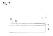
Fig. 1 is a view for explaining a configuration of a processed plate. -
Fig. 2 is a view schematically showing a crystal structure of MgO. -
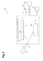
Fig. 3 is a view for explaining a main configuration of a manufacturing apparatus. -
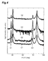
Fig. 4 shows XRD patterns of processed plates according to examples. -
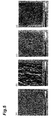
Fig. 5 shows AFM images of processed films according to examples.Fig. 5(a) is with a film thickness of 5 nm,Fig. 5(b) is with a film thickness of 10 nm,Fig. 5(c) is with a film thickness of 20 nm, andFig. 5(d) is with a film thickness of 50 nm. -
Fig. 6(a) is a diagram for explaining characteristics of processed films according to an example, andFig. 6(b) is a diagram for explaining characteristics of processed films according to a comparative example. - Hereinafter, various embodiments will be described in detail with reference to the accompanying drawings. Here, in the description of the drawings, the same elements are denoted by the same reference numerals, and overlapping description will be omitted. Also, dimensional ratios of the drawings are not always coincident with those in the description.
- Description will be given of a configuration of a processed plate according to the present embodiment.
Fig. 1 is a view for explaining the configuration of the processed plate 1. The processed plate 1 includes asubstrate 2 and a processedfilm 3. - The
substrate 2 is a plate-like object formed by an inorganic material, and is preferably a crystalline or amorphous structure formed of one or more of strontium titanate, yttria-stabilized zirconia, and the like. A preferred crystal structure of thesubstrate 2 has three-fold symmetry or six-fold symmetry with respect to a direction along a normal to aprincipal surface 2a. As thesubstrate 2, for example, strontium titanate (SrTiO3) having a (111) plane as its front surface, yttria-stabilized zirconia (YSZ) having a (111) plane as its front surface, or the like can be used. - SrTiO3, which is also called strontium titanium (IV) trioxide, is a complex oxide and has a perovskite type crystal structure. Further, the SrTiO3 or the like that constitutes the
substrate 2 may be doped with an impurity. If a voltage is applied to thesubstrate 2 doped with an impurity, a current flows in thesubstrate 2, so that thesubstrate 2 is heated by resistance heat generation. Accordingly, it becomes possible to control the temperature of the processedfilm 3 by controlling a voltage to be applied to thesubstrate 2. That is, heating of the processedfilm 3 can be easily performed. As the impurity, for example, niobium (Nb) is used. The doping amount of Nb as an impurity is, for example, 0.01 to 0.5 percent by weight. Moreover, thesubstrate 2 has, for example, aprincipal surface 2a which is oriented in (111) as plane orientation. - The processed film is directly formed on the
principal surface 2a of thesubstrate 2. That is, a back surface of the processedfilm 3 and theprincipal surface 2a of thesubstrate 2 are bonded. The processedfilm 3 has afront surface 3 a made of magnesium oxide having a (111) plane as its front surface. The thickness of the processedfilm 3 is, for example, 0.5 to 100 nm. In addition, the thickness of the processedfilm 3 may be a thickness not exceeding 50 nm. Alternatively, the thickness of the processedfilm 3 may be 5 to 20 nm, and may be 7 to 15 nm. - Here, a general MgO crystal structure will be described.
Fig. 2 is a view schematically showing the crystal structure of MgO. MgO has a sodium chloride type crystal structure which is a cubic crystal system, and the plane orientation of the front surface of MgO that naturally occurs is (100). The (100) plane of MgO that has been atomically flattened is a plane having Mg2+ as cations and O2- as anions exposed in equal amounts, and is a stable plane because of being electrically neutral. - On the other hand, the processed
film 3 according to the present embodiment has afront surface 3a consisting of a crystal face CF whose plane orientation is (.111). On the crystal face CF, a plane with only Mg2+ as cations exposed or a plane with only O2- as anions exposed is exposed. For this reason, the crystal face CF is charged to be electrically positive or negative, and is an electrostatically unstable plane. Such a crystal face CF has unique chemical and electrical surface characteristics. For example, the crystal face CF has strong basicity, electron donativity, or catalytic ability. A specific example of the catalytic ability is the ability to adsorb or reduce carbon dioxide (CO2). - The
front surface 3a of the processedfilm 3 has been atomically flattened. Being "atomically flat" is not limited to only where a crystal face is perfectly flat. When a crystal face flattened at the atomic level is actually prepared, the front surface of crystal is minutely inclined when observed at the atomic level. At this time, there is formed a step structure corresponding to an atomic layer on the front surface of crystal. Such a case is also included in the case where the crystal face is "atomically flat." Specifically, the root mean square roughness Rq of thefront surface 3 a of the processedfilm 3 is in a range not exceeding, for example, 1.0 nm. Moreover, the root mean square roughness Rq may be in a range not exceeding 0.5 nm. Rq is calculated by using an atomic force microscope, for example, by scanning an area that is 1 to 2 µm on one side. - Next, description will be given of a manufacturing method for the processed plate 1. For manufacturing of the processed plate 1, for example, a laser abrasion method can be used. According to the laser abrasion method, the processed plate 1 can be manufactured under relatively wide film forming conditions.
-
Fig. 3 is a view for explaining a configuration of amanufacturing apparatus 10. Themanufacturing apparatus 10 includes achamber 11, asubstrate 2, and atarget 12. - The
chamber 11 demarcates inside thereof aprocessing space 11 a that houses thesubstrate 2 and thetarget 12. Thesubstrate 2 is disposed, for example, in an upper part of theprocessing space 11a. Thetarget 12 is disposed in a lower part of theprocessing space 11a. That is, thetarget 12 is disposed in a direction vertically downward with respect to thesubstrate 2, separate from thesubstrate 2. The distance between thetarget 12 and thesubstrate 2 is arbitrary, and it suffices to appropriately select the distance according to the scale of themanufacturing apparatus 10. Thetarget 12 is a raw material for the processedfilm 3 to be formed on theprincipal surface 2a of thesubstrate 2. - In a sidewall of the
chamber 11, awindow 13 arranged to be optically transparent is provided. Alaser light source 15 is disposed outside thechamber 11, and generates laser light L to be irradiated on thetarget 12. Thelaser light source 15 emits the laser light L to thetarget 12 via thewindow 13. - To the
chamber 11, anexhaust device 14 is connected. Theexhaust device 14 decompresses theprocessing space 11a in thechamber 11. Theexhaust device 14 is a predetermined vacuum pump. For example, a turbomolecular pump, an oil diffusion pump, or the like can be used. In this manner, thechamber 11 is arranged to be evacuable. Further, to thechamber 11, agas introduction device 18 is connected. Thegas introduction device 18 includes agas source 19 and avalve 20, and introduces a predetermined gas into theprocessing space 11a of thechamber 11. - Moreover, in the
processing space 11a, aheating device 16 is disposed. Theheating device 16 includes a lamp light source 17. Light from the lamp light source 17 is converged to thesubstrate 2, and can heat the substrate to a predetermined temperature. - Subsequently, description will be given of a process for manufacturing the processed plate 1. First, the
substrate 2 and thetarget 12 are disposed in thechamber 11. In addition, a case where SrTiO3 or YSZ is used as an example of the material for thesubstrate 2 and itsprincipal surface 2a is a (111) plane will be described. Also, a case where a MgO sintered body or a MgO single crystal is used as an example of thetarget 12 will be described. - After disposing the
substrate 2 and thetarget 12 in thechamber 11, the interior of thechamber 11 is decompressed to an order of 10-5 to 10-7 Pa. Subsequently, oxygen gas is injected from the outside using thegas introduction device 18 to set the oxygen partial pressure to an order of, for example, 10-2 to 10-5 Pa. The oxygen partial pressure may be 0.5×10⁻³ to 2.0×10⁻³ Pa. Next, lamp light is converged to thesubstrate 2 from the lamp light source 17 to heat thesubstrate 2 to a predetermined temperature. The predetermined temperature is, for example, 400 to 700 C°. The predetermined temperature may be 600 to 650 C°. - Next, laser light L is irradiated into the
chamber 11 through thewindow 13 of thechamber 11. The laser light L is a pulsed laser light, has a high energy density, and is irradiated to thetarget 12. For example, the laser light L is a KrF excimer laser (krypton fluoride excimer laser) light having a wavelength of 248 nm. The laser light L to be introduced into thechamber 11 has a total energy of 50 mJ or more. Moreover, the total energy of the laser light L may be 50 to 150 mJ. When the laser light L is irradiated to afront surface 12a of thetarget 12, MgO on thefront surface 12a of thetarget 12 is stripped. The stripped MgO is deposited on theprincipal surface 2a of thesubstrate 2a, and is epitaxially grown. The processedfilm 3 is thereby formed. - As above, by directly depositing the processed
film 3 on the (111) plane of SrTiO3 or (111) plane of YSZ and epitaxially growing the same, a processedfilm 3 of the (111) plane is formed, and a processed plate 1 is manufactured. In the case of film formation by a laser abrasion method, energy during film formation is great as compared with that in the case of film formation by a molecular beam epitaxy method or the like. Energy that is great during film formation is considered to contribute to formation of a MgO(111) plane. - In addition, the above-described embodiment is an exemplification of a processed plate and preparation method according to the present invention. The processed plate and preparation method according to the present invention is not limited to the above-described embodiment. The processed plate and preparation method according to the above-described embodiment may be modified or applied to others within a range not changing the gist described in the claims.
- For example, in the above-described embodiment, a description has been given of an example of the
substrate 2 doped with an impurity, but the present invention is not limited thereto. As thesubstrate 2, SrTiO3 or the like doped with no impurity may be used. - Moreover, in the above-described embodiment, a description has been given of an example of the method of heating the
substrate 2 by light from the lamp light source 17 in the manufacturing process for the processed plate 1, but the present invention is not limited thereto. Various methods can be used for heating thesubstrate 2. For example, infrared laser light may be used in place of light from the lamp light source 17. - Hereinafter, examples and comparative examples carried out by the present inventor will be mentioned in order to describe the abovementioned effects.
- Processed plates according to examples were prepared using the
manufacturing apparatus 10 shown inFig. 3 . As the examples, processed films made of MgO having (111) planes as their front surfaces were formed on the principal surfaces of substrates. A specific configuration of themanufacturing apparatus 10 and preparation conditions are as follows.
Target: MgO single crystal target
Substrate: SrTiO3 doped with Nb having a (111) plane at its front surface (The doping amount ofNb is 0.5 percent by weight.)
Laser light source: Excimer laser COMPexPro 201 manufactured by Coherent, Inc.
Laser wavelength: 248 nm
Amount of laser energy: 100 mJ
Laser pulse frequency: 10 Hz - Processed plates according to comparative examples were prepared using the
manufacturing apparatus 10 shown inFig. 3 . A processed films made of MgO having (100) planes as their front surfaces were formed on the principal surfaces of substrates. A specific configuration of themanufacturing apparatus 10 and preparation conditions are the same as those of the examples except for the substrates. - Substrate: SrTiO3 doped with Nb having a (100) plane at its front surface (The doping amount of Nb is 0.5 percent by weight.)
- A structural evaluation of the processed
films 3 according to the examples was performed.Fig. 4 shows X-ray diffraction patterns of processed plates according to the examples. InFig. 4 , graph G1 is a pattern of a processed plate formed when the temperature of the substrate was 400 °C, graph G2 is a pattern of a processed plate formed when the temperature of the substrate was 500 °C, graph G3 is a pattern of a processed plate formed when the temperature of the substrate was 600 °C, and graph G4 is a pattern of a processed plate formed when the temperature of the substrate was 700 °C. Moreover, processed films of these processed plates were formed in an environment where the oxygen partial pressure was 1×10⁻³ Pa. As shown in graph G1 to graph G4, it has been confirmed that under any temperature condition, peaks appear at site D1 indicating a (111) plane of MgO and site D2 indicating a (222) plane. Thereby, it has been confirmed that a processed film made of MgO having a (111) plane as its front surface is formed in a range of the substrate temperature of 400 to 700 °C. Moreover, it has been confirmed that a processed film made of MgO having a (111) plane as its front surface is formed when the amount of laser energy is 100 mJ. When it is considered that energy that is great during film formation contributes to formation of a MgO(111) plane, it can be said to have been suggested that MgO having a (111) plane as its front surface is formed at least with the amount of laser energy of 100 mJ or more. - The front surface of processed films of the processed plates 1 according to the examples was observed using an atomic force microscope. Samples of the examples were prepared as observation objects at a substrate temperature of 600 to 650 °C and an oxygen partial pressure of 1.5×10⁻³ Pa during processed film formation. As the atomic force microscope, SPI3800N Probe Station manufactured by SII NanoTechnology Inc. was used. As measurement conditions, 2 micrometers square of the sample front surfaces were observed in the atmosphere. The results are shown in
Fig. 5. Fig. 5(a) is an AFM image of a processed film of a processed plate according to the example with a film thickness of 5 nm,Fig. 5(b) is an AFM image with a film thickness of 10 nm,Fig. 5(c) is an AFM image with a film thickness of 20 nm, andFig. 5(d) is an AFM image with a film thickness of 50 nm. InFig. 5(a) , the blackest part expresses 0.81 nm, and the whitest part expresses 1.36 nm. InFig. 5(b) , the blackest part expresses 0.00 nm, and the whitest part expresses 1.89 nm. InFig. 5(c) , the blackest part expresses 0.00 nm, and the whitest part expresses 2.98 nm. InFig. 5(d) , the blackest part expresses 0.00 nm, and the whitest part expresses 13.31 nm. As shown in the AFM images shown inFigs. 5(a) to (c) , it could be confirmed that the front surfaces of MgO(111) having film thicknesses of 5 nm to 20 nm have grown as films with little unevenness. On the other hand, it could be confirmed that the front surface of MgO(111) having a film thickness of 50 nm has grown as a film with relatively much unevenness. Moreover, the root mean square roughness Rq was measured with the measurement of AFM images. The root mean square roughness Rq was 0.3037 nm with a film thickness of 5 nm, the root mean square roughness Rq was 0.2992 nm with a film thickness of 10 nm, the root mean square roughness Rq was 0.4702 nm with a film thickness of 20 nm, the root mean square roughness Rq was 1.580 nm with a film thickness of 20 nm. As indicated by the measurement results of the root mean square roughness Rq, it has been confirmed that the processed films of the processed plates 1 according to the examples have a root mean square roughness Rq of 0.5 nm or less in a range of the film thickness not exceeding 50 nm, and are flat surfaces. It has been specifically confirmed that, when the film thickness is 5 nm to 20 nm, the processed film has a root mean square roughness Rq of 0.5 nm or less and is a flat surface. - Surface characteristics of the processed plate 1 according to the example and the processed plate according to the comparative example were evaluated. As an adsorbate of an adsorption experiment to evaluate chemical properties (acidity and basicity) of the front surface of the substrate, CO2 or NH3 has been most normally adopted. CO2 was used here to evaluate adsorption characteristics and reduction characteristics. In this evaluation, adsorption characteristics of CO2, that is, the basicity of the front surface was evaluated by measuring gas thermal desorption characteristics of CO2. Moreover, reduction characteristics of CO2, that is, the degree of chemical activity was evaluated by measuring gas thermal desorption characteristics of CO. The gas thermal desorption characteristics were measured using quadrupole mass spectrometry. The quadrupole mass spectrometry is a method of adding perturbation to ions by passing ions through four electrode tubes applied with a high-frequency voltage, passing only desired ions therethrough, and measuring the mass of the passed ions. In this evaluation, a processed plate including a processed film with a thickness of 50 nm prepared in a state where the substrate temperature was 650 °C was used as the example. On the other hand, a processed plate including a processed film with a thickness of 5 nm prepared in a state where the substrate temperature was 650 °C was used as the comparative example.
-
Fig. 6(a) shows gas thermal desorption characteristics of CO2 and CO of the processed plate according to the example. InFig. 6(a) , graph G5 shows gas thermal desorption characteristics of CO2, and graph G6 shows gas thermal desorption characteristics of CO. As shown in graph G5, it has been confirmed that desorption of CO2 from thefront surface 3a occurred from around 50 °C. Moreover, as shown in graph G6, it has been confirmed that CO2 on thefront surface 3a is reduced to produce CO from around 50 °C, and further, a large amount of CO was produced from around 100 °C. Thus, it has been confirmed that, in the CO2 reduction method using the processedfilm 3, a reduction of CO2 proceeds on thefront surface 3a without irradiation of ultraviolet rays or the like. That is, because a reduction of carbon dioxide occurred at a relatively low temperature of 50 °C to 100 °C, it has been confirmed that the processed film of the processed plate according to the example has strong basicity. -
Fig. 6(b) shows gas thermal desorption characteristics of CO2 and CO of the processed plate according to the comparative example. InFig. 6(b) , graph G7 shows gas thermal desorption characteristics of CO2, and graph G8 shows gas thermal desorption characteristics of CO. As shown in graph G7, it has been confirmed that desorption of CO2 from the front surface occurred from around 50 °C. On the other hand, as shown in graph G8, the production of CO is almost zero, and it has been confirmed that CO is not produced because CO2 is not reduced even by heating the processed film. - Then, it has been confirmed by a comparison of graph G5 with graph G7 that the amount of CO2 desorption from the processed film according to the example is larger than the amount of CO2 desorption from the processed film according to the comparative example. Thus, it has been confirmed that the processed film having a front surface consisting of a (111) plane of MgO can efficiently adsorb CO2 as compared with the processed film having a front surface consisting of a (100) plane of MgO. That is, it has been confirmed that the processed film of the processed plate according to the example is stronger in the basicity of the front surface than the processed film of the processed plate according to the comparative example.
- Conventionally, as thin-film substrates, MgO substrates having naturally occurring (100) planes as their front surfaces have been used. On the other hand, the lattice constant of a (111) plane of MgO is different from the lattice constant of a currently commercially available substrate on the front surface of which a triangular lattice is formed. Thus, the processed plate 1 according to the present embodiment is useful as a new thin-film growth substrate for electronics.
- Further, conventionally, a thin-film growth substrate has been selected by mainly focusing on the matching of lattice constants, not by focusing on the catalytic ability etc., on the front surface of the substrate. On the other hand, the processed plate 1 according to the present embodiment has strong basicity and chemical activity caused by polarization in the vertical direction to the front surface of the substrate. Therefore, it is possible to have added value as a substrate for crystal growth of a thin film or the like. For example, the processed plate 1 according to the present embodiment may be adopted as a substrate for thin-film growth by a soft solution process or as a substrate for CVD. Moreover, the electronic state of a thin film can also be modulated, after preparing a thin film on the processed plate 1 according to the present embodiment, by using polarization of the processed film of said processed plate 1. Moreover, a natural growth surface of the magnetite Fe3O4 described in Non-Patent Document 1 is not a (100) plane but a (111) plane or a (110) plane. It is therefore expected that forming Fe3O4 on the processed plate 1 according to the present embodiment allows preparation of an Fe3O4 film of higher quality. Moreover, because it is presumably considered that neither of the (111) planes of MgO described in
Non-Patent Documents Non-Patent Documents Non-Patent Document 2. Moreover, taking advantage of being a flat surface, it can be suitably adopted for a device for which the interface roughness needs to be suppressed, such as a magnetic tunnel junction element. Further, the processed plate 1 according to the present embodiment is also useful as a substrate of the ferroelectric thin film described inNon-Patent Document 3. Moreover, taking advantage of being a (111) film of MgO and being a flat surface, the film thickness of a dielectric thin film having desired characteristics can be reliably reduced. Further, the processed plate 1 can be used for, for example, a processing having a process of causing reaction of molecules while depositing on the substrate like MOCVD or the like. - Further, as a catalyst, a rare metal such as platinum or palladium or a hybrid of a rare metal and an oxide has been used. However, these substances are rare and are also toxic in some cases. On the other hand, the processed plate 1 according to the present embodiment uses MgO. MgO is a common substance and is nontoxic. Thus, there is no need for concern about environmental pollution with the processed plate 1 according to the present embodiment. Further, because MgO has no toxicity to living organisms, the processed plate 1 according to the present embodiment can be used for selective adsorption of acid molecules in living organisms. For example, the processed plate 1 according to the present embodiment can be applied as a so-called biosensor, which is a detection element for biomolecules (protein, viruses, amino acids). Specifically, biomolecules can be detected based on a change in electrical conductivity of the processed plate 1 before and after adsorption of biomolecules. Accordingly, usage as a diagnostic drug or a test drug is available.
- Also, CO2 has continuously increased due to the use of fossil fuels. Because the CO2 is chemically extremely stable, it is not easy to alter CO2 to another chemical species under conditions of the atmospheric pressure and room temperature. Therefore, a method for collecting and confining or effectively using CO2 been studied. By the processed plate 1 according to the present embodiment, CO2 can be efficiently adsorbed. Thus, it becomes possible to easily store CO2.
- Further, by the processed plate 1 according to the present embodiment 1, it is possible to reduce CO2 to CO by causing CO2 to be adsorbed on the processed film and then heating the processed film. Thus, because CO2 can be easily reduced, it becomes possible to realize a reaction process using CO2 as a starting material. Thus, CO2 can be effectively used.
- Moreover, the processed film of the processed plate 1 according to the present embodiment is formed on a substrate. Therefore, handling of the processed plate can be made easy. Further, the processed film can be coupled with another member via the substrate. Furthermore, when the substrate is one doped with an impurity to have conductivity, it is possible to easily control the temperature of the processed film by controlling a voltage to be applied to the substrate. Temperature control of the processed film allows easily controlling adsorption or reduction (desorption) of CO2 in the processed film. Moreover, in the case of, for example, a substrate with low light transmittance, such as a substrate in a blackish color, it is considered that the substrate temperature rises to an order of 50 °C when the substrate is irradiated with sunlight. According thereto, adsorption or reduction (desorption) of CO2 is performed on the processed film without artificially injecting energy. Therefore, CO2 exhaled by plants in the nighttime can be adsorbed and stored using the processed plate, and the CO2 can be desorbed from the processed plate in the daytime to be used as a raw material for photosynthesis.
- 1... processed plate, 2... substrate, 3... processed film, 5 processing apparatus, 10... manufacturing apparatus, 11, 21... chamber, 12... target, 13... window, 14... exhaust device, 15... laser light source, 16, 25... heating device, 17... lamp light source, 18... gas introduction device, G1 to G8... graphs, L... laser light.
Claims (12)
- A preparation method for a magnesium oxide thin film which is a method for depositing a magnesium oxide thin film on a substrate by a laser abrasion method using a sintered body or single crystal of magnesium oxide as a target, wherein
a flat processed film made of magnesium oxide having a (111) plane as its front surface is prepared, using a substrate made of strontium titanate having a (111) plane as its principal surface or yttria-stabilized zirconia having a (111) plane as its principal surface, by directly depositing a film on the principal surface of the substrate and epitaxially growing the film. - The preparation method for a magnesium oxide thin film according to claim 1, wherein the processed film has a root mean square roughness Rq of a magnesium oxide (111) plane not exceeding 1 nm.
- The preparation method for a magnesium oxide thin film according to claim 2, wherein the processed film is a film having a root mean square roughness Rq of a magnesium oxide (111) plane not exceeding 0.5 nm.
- The preparation method for a magnesium oxide thin film according to any one of claims 1 to 3, wherein an amount of laser energy in the laser abrasion method is 50 mJ or more.
- The preparation method for a magnesium oxide thin film according to any one of claims 1 to 4, wherein the processed film is a film having a film thickness not exceeding 50 nm.
- The preparation method for a magnesium oxide thin film according to any one of claims 1 to 5, wherein a substrate temperature during film formation of the processed film is 600 to 650 °C.
- The preparation method for a magnesium oxide thin film according to any one of claims 1 to 6, wherein an oxygen partial pressure during film formation of the processed film is 0.5×10⁻³ to 2.0×10⁻³ Pa.
- A processed plate including:a substrate made of strontium titanate having a (111) plane as its principal surface or yttria-stabilized zirconia having a (111) plane as its principal surface; anda flat processed film directly formed on the principal surface of the substrate and made of magnesium oxide having a (111) plane as its front surface.
- The processed plate according to claim 8, wherein the processed film is a film having a root mean square roughness Rq of a (111) plane of magnesium oxide not exceeding 1 nm.
- The processed plate according to claim 9, wherein the processed film is a film having a root mean square roughness Rq of a magnesium oxide (111) plane not exceeding 0.5 nm.
- The processed plate according to any one of claims 8 to 10, wherein the processed film is a film having a film thickness not exceeding 50 nm.
- A device using as an adsorption surface the processed film of the processed plate according to any one of claims 8 to 11.
Applications Claiming Priority (2)
| Application Number | Priority Date | Filing Date | Title |
|---|---|---|---|
| JP2011197562A JP2013056323A (en) | 2011-09-09 | 2011-09-09 | Treatment plate, and treatment method |
| PCT/JP2012/056191 WO2013035360A1 (en) | 2011-09-09 | 2012-03-09 | Method for forming magnesium oxide thin film and processed plate |
Publications (3)
| Publication Number | Publication Date |
|---|---|
| EP2754737A1 true EP2754737A1 (en) | 2014-07-16 |
| EP2754737A4 EP2754737A4 (en) | 2015-07-29 |
| EP2754737B1 EP2754737B1 (en) | 2017-08-09 |
Family
ID=47831827
Family Applications (1)
| Application Number | Title | Priority Date | Filing Date |
|---|---|---|---|
| EP12829861.9A Not-in-force EP2754737B1 (en) | 2011-09-09 | 2012-03-09 | Method for forming a magnesium oxide thin film |
Country Status (5)
| Country | Link |
|---|---|
| US (1) | US9605357B2 (en) |
| EP (1) | EP2754737B1 (en) |
| JP (1) | JP2013056323A (en) |
| KR (1) | KR101745979B1 (en) |
| WO (1) | WO2013035360A1 (en) |
Families Citing this family (1)
| Publication number | Priority date | Publication date | Assignee | Title |
|---|---|---|---|---|
| JP7759048B2 (en) * | 2021-08-19 | 2025-10-23 | 国立大学法人埼玉大学 | Magnesium oxide substrate manufacturing method |
Family Cites Families (4)
| Publication number | Priority date | Publication date | Assignee | Title |
|---|---|---|---|---|
| JP4014473B2 (en) | 2002-08-30 | 2007-11-28 | 独立行政法人科学技術振興機構 | Method for manufacturing ultra-flat p-type oxide semiconductor NiO single crystal thin film |
| JP2007246354A (en) | 2006-03-17 | 2007-09-27 | Japan Science & Technology Agency | Thin film substrate manufacturing method |
| JP2010107299A (en) * | 2008-10-29 | 2010-05-13 | Ngk Spark Plug Co Ltd | Infrared detection element, sensor, and method for manufacturing infrared detection element |
| JP5765678B2 (en) * | 2010-02-25 | 2015-08-19 | 三菱化学株式会社 | Photocatalyst for photowater splitting reaction and method for producing photocatalyst for photowater splitting reaction |
-
2011
- 2011-09-09 JP JP2011197562A patent/JP2013056323A/en active Pending
-
2012
- 2012-03-09 KR KR1020147006777A patent/KR101745979B1/en not_active Expired - Fee Related
- 2012-03-09 WO PCT/JP2012/056191 patent/WO2013035360A1/en not_active Ceased
- 2012-03-09 US US14/343,719 patent/US9605357B2/en not_active Expired - Fee Related
- 2012-03-09 EP EP12829861.9A patent/EP2754737B1/en not_active Not-in-force
Non-Patent Citations (5)
| Title |
|---|
| KOSUKE MATSUZAKI ET AL: ""Structural study of polar MgO(111) epitaxial thin films grown on SrTiO3(111)"", PHYSICAL REVIEW B, vol. 84, no. 23, 1 December 2011 (2011-12-01), XP055198163, ISSN: 1098-0121, DOI: 10.1103/PhysRevB.84.235448 * |
| None * |
| See also references of WO2013035360A1 * |
| SHO KUMADA ET AL: "Tuning of Surface Roughness and Lattice Constant in MgO(111)/Al2O3(0001) Grown by Laser Energy Controlled Pulsed Laser Deposition", JAPANESE JOURNAL OF APPLIED PHYSICS, vol. 50, no. 8, 22 August 2011 (2011-08-22), pages 085503, XP055198178, ISSN: 0021-4922, DOI: 10.1143/JJAP.50.085503 * |
| TADAHIRO FUJIHASHI ET AL: "C02 o Probe to shita MgO/Nb:SrTiO3(111) Hyomen Tokusei no Kansatsu = MgO/Nb:SrTiO3(111) surface properties studied by CO2 adsorption", EXTENDED ABSTRACTS, MEETING OF THE JAPAN SOCIETY OF APPLIED PHYSICS AND RELATED SOCIETIES,, vol. 58, 24 March 2011 (2011-03-24), pages 24P - BC, XP008174038 * |
Also Published As
| Publication number | Publication date |
|---|---|
| US20140230724A1 (en) | 2014-08-21 |
| US9605357B2 (en) | 2017-03-28 |
| WO2013035360A1 (en) | 2013-03-14 |
| KR101745979B1 (en) | 2017-06-12 |
| KR20140059813A (en) | 2014-05-16 |
| JP2013056323A (en) | 2013-03-28 |
| CN103781949A (en) | 2014-05-07 |
| EP2754737B1 (en) | 2017-08-09 |
| EP2754737A4 (en) | 2015-07-29 |
Similar Documents
| Publication | Publication Date | Title |
|---|---|---|
| Chambers | Epitaxial growth and properties of doped transition metal and complex oxide films | |
| Kubicek et al. | Tensile lattice strain accelerates oxygen surface exchange and diffusion in La1–xSrxCoO3− δ thin films | |
| Pan et al. | Spontaneous growth of ZnCO3 nanowires on ZnO nanostructures in normal ambient environment: unstable ZnO nanostructures | |
| Bliem et al. | Hf deposition stabilizes the surface chemistry of perovskite manganite oxide | |
| Yang et al. | Tuning Ionic Conductivity in Fluorite Gd-Doped CeO2‑Bixbyite RE2O3 (RE= Y and Sm) Multilayer Thin Films by Controlling Interfacial Strain | |
| Peter et al. | Role of hydrogen-related defects in photocatalytic activity of ZnO films grown by atomic layer deposition | |
| Brand et al. | Defect-induced magnetic symmetry breaking in oxide materials | |
| Chen et al. | Impact of microstructure and crystallinity on surface exchange kinetics of strontium titanium iron oxide perovskite by in situ optical transmission relaxation approach | |
| Yoo et al. | Unraveling crystal structure and transport properties of fast ion conducting SrCo0. 9Nb0. 1O3− δ | |
| Boileau et al. | Inductive effect of Nd for Ni3+ stabilization in NdNiO3 synthesized by reactive DC cosputtering | |
| EP2754737B1 (en) | Method for forming a magnesium oxide thin film | |
| Pan et al. | Giant piezoresponse and promising application of environmental friendly small-ion-doped ZnO | |
| Raisch et al. | Preparation and investigation of the A-site and B-site terminated SrTiO3 (001) surface: A combined experimental and theoretical x-ray photoelectron diffraction study | |
| JP5246900B1 (en) | Method for making magnesium oxide thin film | |
| Sallet et al. | Why is it difficult to grow spontaneous ZnO nanowires using molecular beam epitaxy? | |
| Tran et al. | A novel approach for fabricating LaMnO3 thin films using combined microwave combustion and pulsed electron deposition techniques | |
| CN103781949B (en) | The manufacture method of magnesia film and process plate | |
| Wells et al. | Novel electrostatic dry lift-off and transfer route for vertically aligned nanocomposite oxide thin films | |
| JP2005053755A (en) | Oxide epitaxial thin film and method for producing the same | |
| Sata et al. | Synthesis of La0. 6Sr0. 4FeO3/La0. 6Sr0. 4CoO3 mixed ion conducting superlattices by PLD | |
| Chen et al. | Relating microstructure to surface exchange kinetics using in situ optical absorption relaxation | |
| TWI878214B (en) | Solid electrolyte junction | |
| Huo | Epitaxial growth structure and optical electrical property of tin oxide films with hollow cathode gas flow sputtering technology | |
| Thapa | Surface and interfacial studies of perovskite oxides grown by hybrid molecular beam epitaxy | |
| Flack | Thin film components for solid oxide fuel Cells (SOFCs) |
Legal Events
| Date | Code | Title | Description |
|---|---|---|---|
| PUAI | Public reference made under article 153(3) epc to a published international application that has entered the european phase |
Free format text: ORIGINAL CODE: 0009012 |
|
| 17P | Request for examination filed |
Effective date: 20140403 |
|
| AK | Designated contracting states |
Kind code of ref document: A1 Designated state(s): AL AT BE BG CH CY CZ DE DK EE ES FI FR GB GR HR HU IE IS IT LI LT LU LV MC MK MT NL NO PL PT RO RS SE SI SK SM TR |
|
| DAX | Request for extension of the european patent (deleted) | ||
| RA4 | Supplementary search report drawn up and despatched (corrected) |
Effective date: 20150701 |
|
| RIC1 | Information provided on ipc code assigned before grant |
Ipc: B01D 53/02 20060101ALI20150625BHEP Ipc: B01D 53/04 20060101ALI20150625BHEP Ipc: C23C 14/08 20060101ALI20150625BHEP Ipc: B01J 20/04 20060101ALI20150625BHEP Ipc: C30B 29/16 20060101AFI20150625BHEP Ipc: C23C 14/28 20060101ALI20150625BHEP Ipc: B01J 21/10 20060101ALI20150625BHEP Ipc: C30B 23/06 20060101ALI20150625BHEP |
|
| REG | Reference to a national code |
Ref country code: DE Ref legal event code: R079 Ref document number: 602012035791 Country of ref document: DE Free format text: PREVIOUS MAIN CLASS: C30B0029160000 Ipc: B01J0020040000 |
|
| GRAP | Despatch of communication of intention to grant a patent |
Free format text: ORIGINAL CODE: EPIDOSNIGR1 |
|
| STAA | Information on the status of an ep patent application or granted ep patent |
Free format text: STATUS: GRANT OF PATENT IS INTENDED |
|
| RIC1 | Information provided on ipc code assigned before grant |
Ipc: C30B 23/06 20060101ALI20170331BHEP Ipc: C30B 23/02 20060101ALI20170331BHEP Ipc: C30B 29/16 20060101ALI20170331BHEP Ipc: B01J 20/04 20060101AFI20170331BHEP Ipc: B01J 20/32 20060101ALI20170331BHEP Ipc: B01D 53/02 20060101ALI20170331BHEP |
|
| INTG | Intention to grant announced |
Effective date: 20170426 |
|
| RIN1 | Information on inventor provided before grant (corrected) |
Inventor name: FUJIHASHI, TADAHIRO Inventor name: SUSAKI, TOMOFUMI Inventor name: HOSONO, HIDEO Inventor name: TODA, YOSHITAKE |
|
| GRAS | Grant fee paid |
Free format text: ORIGINAL CODE: EPIDOSNIGR3 |
|
| GRAA | (expected) grant |
Free format text: ORIGINAL CODE: 0009210 |
|
| STAA | Information on the status of an ep patent application or granted ep patent |
Free format text: STATUS: THE PATENT HAS BEEN GRANTED |
|
| AK | Designated contracting states |
Kind code of ref document: B1 Designated state(s): AL AT BE BG CH CY CZ DE DK EE ES FI FR GB GR HR HU IE IS IT LI LT LU LV MC MK MT NL NO PL PT RO RS SE SI SK SM TR |
|
| REG | Reference to a national code |
Ref country code: GB Ref legal event code: FG4D |
|
| REG | Reference to a national code |
Ref country code: CH Ref legal event code: EP Ref country code: AT Ref legal event code: REF Ref document number: 916224 Country of ref document: AT Kind code of ref document: T Effective date: 20170815 |
|
| REG | Reference to a national code |
Ref country code: IE Ref legal event code: FG4D |
|
| REG | Reference to a national code |
Ref country code: DE Ref legal event code: R096 Ref document number: 602012035791 Country of ref document: DE |
|
| REG | Reference to a national code |
Ref country code: NL Ref legal event code: MP Effective date: 20170809 |
|
| REG | Reference to a national code |
Ref country code: LT Ref legal event code: MG4D |
|
| REG | Reference to a national code |
Ref country code: AT Ref legal event code: MK05 Ref document number: 916224 Country of ref document: AT Kind code of ref document: T Effective date: 20170809 |
|
| PG25 | Lapsed in a contracting state [announced via postgrant information from national office to epo] |
Ref country code: HR Free format text: LAPSE BECAUSE OF FAILURE TO SUBMIT A TRANSLATION OF THE DESCRIPTION OR TO PAY THE FEE WITHIN THE PRESCRIBED TIME-LIMIT Effective date: 20170809 Ref country code: NL Free format text: LAPSE BECAUSE OF FAILURE TO SUBMIT A TRANSLATION OF THE DESCRIPTION OR TO PAY THE FEE WITHIN THE PRESCRIBED TIME-LIMIT Effective date: 20170809 Ref country code: SE Free format text: LAPSE BECAUSE OF FAILURE TO SUBMIT A TRANSLATION OF THE DESCRIPTION OR TO PAY THE FEE WITHIN THE PRESCRIBED TIME-LIMIT Effective date: 20170809 Ref country code: LT Free format text: LAPSE BECAUSE OF FAILURE TO SUBMIT A TRANSLATION OF THE DESCRIPTION OR TO PAY THE FEE WITHIN THE PRESCRIBED TIME-LIMIT Effective date: 20170809 Ref country code: FI Free format text: LAPSE BECAUSE OF FAILURE TO SUBMIT A TRANSLATION OF THE DESCRIPTION OR TO PAY THE FEE WITHIN THE PRESCRIBED TIME-LIMIT Effective date: 20170809 Ref country code: NO Free format text: LAPSE BECAUSE OF FAILURE TO SUBMIT A TRANSLATION OF THE DESCRIPTION OR TO PAY THE FEE WITHIN THE PRESCRIBED TIME-LIMIT Effective date: 20171109 Ref country code: AT Free format text: LAPSE BECAUSE OF FAILURE TO SUBMIT A TRANSLATION OF THE DESCRIPTION OR TO PAY THE FEE WITHIN THE PRESCRIBED TIME-LIMIT Effective date: 20170809 |
|
| PG25 | Lapsed in a contracting state [announced via postgrant information from national office to epo] |
Ref country code: GR Free format text: LAPSE BECAUSE OF FAILURE TO SUBMIT A TRANSLATION OF THE DESCRIPTION OR TO PAY THE FEE WITHIN THE PRESCRIBED TIME-LIMIT Effective date: 20171110 Ref country code: IS Free format text: LAPSE BECAUSE OF FAILURE TO SUBMIT A TRANSLATION OF THE DESCRIPTION OR TO PAY THE FEE WITHIN THE PRESCRIBED TIME-LIMIT Effective date: 20171209 Ref country code: RS Free format text: LAPSE BECAUSE OF FAILURE TO SUBMIT A TRANSLATION OF THE DESCRIPTION OR TO PAY THE FEE WITHIN THE PRESCRIBED TIME-LIMIT Effective date: 20170809 Ref country code: PL Free format text: LAPSE BECAUSE OF FAILURE TO SUBMIT A TRANSLATION OF THE DESCRIPTION OR TO PAY THE FEE WITHIN THE PRESCRIBED TIME-LIMIT Effective date: 20170809 Ref country code: LV Free format text: LAPSE BECAUSE OF FAILURE TO SUBMIT A TRANSLATION OF THE DESCRIPTION OR TO PAY THE FEE WITHIN THE PRESCRIBED TIME-LIMIT Effective date: 20170809 Ref country code: ES Free format text: LAPSE BECAUSE OF FAILURE TO SUBMIT A TRANSLATION OF THE DESCRIPTION OR TO PAY THE FEE WITHIN THE PRESCRIBED TIME-LIMIT Effective date: 20170809 Ref country code: BG Free format text: LAPSE BECAUSE OF FAILURE TO SUBMIT A TRANSLATION OF THE DESCRIPTION OR TO PAY THE FEE WITHIN THE PRESCRIBED TIME-LIMIT Effective date: 20171109 |
|
| REG | Reference to a national code |
Ref country code: FR Ref legal event code: PLFP Year of fee payment: 7 |
|
| PG25 | Lapsed in a contracting state [announced via postgrant information from national office to epo] |
Ref country code: CZ Free format text: LAPSE BECAUSE OF FAILURE TO SUBMIT A TRANSLATION OF THE DESCRIPTION OR TO PAY THE FEE WITHIN THE PRESCRIBED TIME-LIMIT Effective date: 20170809 Ref country code: RO Free format text: LAPSE BECAUSE OF FAILURE TO SUBMIT A TRANSLATION OF THE DESCRIPTION OR TO PAY THE FEE WITHIN THE PRESCRIBED TIME-LIMIT Effective date: 20170809 Ref country code: DK Free format text: LAPSE BECAUSE OF FAILURE TO SUBMIT A TRANSLATION OF THE DESCRIPTION OR TO PAY THE FEE WITHIN THE PRESCRIBED TIME-LIMIT Effective date: 20170809 |
|
| REG | Reference to a national code |
Ref country code: DE Ref legal event code: R097 Ref document number: 602012035791 Country of ref document: DE |
|
| PG25 | Lapsed in a contracting state [announced via postgrant information from national office to epo] |
Ref country code: SM Free format text: LAPSE BECAUSE OF FAILURE TO SUBMIT A TRANSLATION OF THE DESCRIPTION OR TO PAY THE FEE WITHIN THE PRESCRIBED TIME-LIMIT Effective date: 20170809 Ref country code: SK Free format text: LAPSE BECAUSE OF FAILURE TO SUBMIT A TRANSLATION OF THE DESCRIPTION OR TO PAY THE FEE WITHIN THE PRESCRIBED TIME-LIMIT Effective date: 20170809 Ref country code: IT Free format text: LAPSE BECAUSE OF FAILURE TO SUBMIT A TRANSLATION OF THE DESCRIPTION OR TO PAY THE FEE WITHIN THE PRESCRIBED TIME-LIMIT Effective date: 20170809 Ref country code: EE Free format text: LAPSE BECAUSE OF FAILURE TO SUBMIT A TRANSLATION OF THE DESCRIPTION OR TO PAY THE FEE WITHIN THE PRESCRIBED TIME-LIMIT Effective date: 20170809 |
|
| PLBE | No opposition filed within time limit |
Free format text: ORIGINAL CODE: 0009261 |
|
| STAA | Information on the status of an ep patent application or granted ep patent |
Free format text: STATUS: NO OPPOSITION FILED WITHIN TIME LIMIT |
|
| 26N | No opposition filed |
Effective date: 20180511 |
|
| PG25 | Lapsed in a contracting state [announced via postgrant information from national office to epo] |
Ref country code: SI Free format text: LAPSE BECAUSE OF FAILURE TO SUBMIT A TRANSLATION OF THE DESCRIPTION OR TO PAY THE FEE WITHIN THE PRESCRIBED TIME-LIMIT Effective date: 20170809 |
|
| REG | Reference to a national code |
Ref country code: CH Ref legal event code: PL |
|
| PG25 | Lapsed in a contracting state [announced via postgrant information from national office to epo] |
Ref country code: MC Free format text: LAPSE BECAUSE OF FAILURE TO SUBMIT A TRANSLATION OF THE DESCRIPTION OR TO PAY THE FEE WITHIN THE PRESCRIBED TIME-LIMIT Effective date: 20170809 |
|
| REG | Reference to a national code |
Ref country code: BE Ref legal event code: MM Effective date: 20180331 |
|
| REG | Reference to a national code |
Ref country code: IE Ref legal event code: MM4A |
|
| PG25 | Lapsed in a contracting state [announced via postgrant information from national office to epo] |
Ref country code: LU Free format text: LAPSE BECAUSE OF NON-PAYMENT OF DUE FEES Effective date: 20180309 |
|
| PG25 | Lapsed in a contracting state [announced via postgrant information from national office to epo] |
Ref country code: IE Free format text: LAPSE BECAUSE OF NON-PAYMENT OF DUE FEES Effective date: 20180309 |
|
| PG25 | Lapsed in a contracting state [announced via postgrant information from national office to epo] |
Ref country code: BE Free format text: LAPSE BECAUSE OF NON-PAYMENT OF DUE FEES Effective date: 20180331 Ref country code: LI Free format text: LAPSE BECAUSE OF NON-PAYMENT OF DUE FEES Effective date: 20180331 Ref country code: CH Free format text: LAPSE BECAUSE OF NON-PAYMENT OF DUE FEES Effective date: 20180331 |
|
| PG25 | Lapsed in a contracting state [announced via postgrant information from national office to epo] |
Ref country code: MT Free format text: LAPSE BECAUSE OF NON-PAYMENT OF DUE FEES Effective date: 20180309 |
|
| PG25 | Lapsed in a contracting state [announced via postgrant information from national office to epo] |
Ref country code: TR Free format text: LAPSE BECAUSE OF FAILURE TO SUBMIT A TRANSLATION OF THE DESCRIPTION OR TO PAY THE FEE WITHIN THE PRESCRIBED TIME-LIMIT Effective date: 20170809 |
|
| PGFP | Annual fee paid to national office [announced via postgrant information from national office to epo] |
Ref country code: GB Payment date: 20200210 Year of fee payment: 9 Ref country code: DE Payment date: 20200206 Year of fee payment: 9 |
|
| PG25 | Lapsed in a contracting state [announced via postgrant information from national office to epo] |
Ref country code: HU Free format text: LAPSE BECAUSE OF FAILURE TO SUBMIT A TRANSLATION OF THE DESCRIPTION OR TO PAY THE FEE WITHIN THE PRESCRIBED TIME-LIMIT; INVALID AB INITIO Effective date: 20120309 Ref country code: PT Free format text: LAPSE BECAUSE OF FAILURE TO SUBMIT A TRANSLATION OF THE DESCRIPTION OR TO PAY THE FEE WITHIN THE PRESCRIBED TIME-LIMIT Effective date: 20170809 |
|
| PG25 | Lapsed in a contracting state [announced via postgrant information from national office to epo] |
Ref country code: CY Free format text: LAPSE BECAUSE OF FAILURE TO SUBMIT A TRANSLATION OF THE DESCRIPTION OR TO PAY THE FEE WITHIN THE PRESCRIBED TIME-LIMIT Effective date: 20170809 Ref country code: MK Free format text: LAPSE BECAUSE OF NON-PAYMENT OF DUE FEES Effective date: 20170809 |
|
| PGFP | Annual fee paid to national office [announced via postgrant information from national office to epo] |
Ref country code: FR Payment date: 20200210 Year of fee payment: 9 |
|
| PG25 | Lapsed in a contracting state [announced via postgrant information from national office to epo] |
Ref country code: AL Free format text: LAPSE BECAUSE OF FAILURE TO SUBMIT A TRANSLATION OF THE DESCRIPTION OR TO PAY THE FEE WITHIN THE PRESCRIBED TIME-LIMIT Effective date: 20170809 |
|
| REG | Reference to a national code |
Ref country code: DE Ref legal event code: R119 Ref document number: 602012035791 Country of ref document: DE |
|
| GBPC | Gb: european patent ceased through non-payment of renewal fee |
Effective date: 20210309 |
|
| PG25 | Lapsed in a contracting state [announced via postgrant information from national office to epo] |
Ref country code: GB Free format text: LAPSE BECAUSE OF NON-PAYMENT OF DUE FEES Effective date: 20210309 Ref country code: FR Free format text: LAPSE BECAUSE OF NON-PAYMENT OF DUE FEES Effective date: 20210331 Ref country code: DE Free format text: LAPSE BECAUSE OF NON-PAYMENT OF DUE FEES Effective date: 20211001 |