EP2750491A1 - Substrate with built-in component and method of manufacturing same - Google Patents
Substrate with built-in component and method of manufacturing same Download PDFInfo
- Publication number
- EP2750491A1 EP2750491A1 EP12825582.5A EP12825582A EP2750491A1 EP 2750491 A1 EP2750491 A1 EP 2750491A1 EP 12825582 A EP12825582 A EP 12825582A EP 2750491 A1 EP2750491 A1 EP 2750491A1
- Authority
- EP
- European Patent Office
- Prior art keywords
- face
- substrate
- wiring board
- component
- layer
- Prior art date
- Legal status (The legal status is an assumption and is not a legal conclusion. Google has not performed a legal analysis and makes no representation as to the accuracy of the status listed.)
- Granted
Links
Images







Classifications
-
- H—ELECTRICITY
- H05—ELECTRIC TECHNIQUES NOT OTHERWISE PROVIDED FOR
- H05K—PRINTED CIRCUITS; CASINGS OR CONSTRUCTIONAL DETAILS OF ELECTRIC APPARATUS; MANUFACTURE OF ASSEMBLAGES OF ELECTRICAL COMPONENTS
- H05K1/00—Printed circuits
- H05K1/18—Printed circuits structurally associated with non-printed electric components
- H05K1/182—Printed circuits structurally associated with non-printed electric components associated with components mounted in printed circuit boards [PCB], e.g. insert-mounted components [IMC]
- H05K1/185—Printed circuits structurally associated with non-printed electric components associated with components mounted in printed circuit boards [PCB], e.g. insert-mounted components [IMC] associated with components encapsulated in the insulating substrate of the PCBs; associated with components incorporated in internal layers of multilayer circuit boards
- H05K1/186—Printed circuits structurally associated with non-printed electric components associated with components mounted in printed circuit boards [PCB], e.g. insert-mounted components [IMC] associated with components encapsulated in the insulating substrate of the PCBs; associated with components incorporated in internal layers of multilayer circuit boards manufactured by mounting on or connecting to patterned circuits before or during embedding
-
- B—PERFORMING OPERATIONS; TRANSPORTING
- B29—WORKING OF PLASTICS; WORKING OF SUBSTANCES IN A PLASTIC STATE IN GENERAL
- B29C—SHAPING OR JOINING OF PLASTICS; SHAPING OF MATERIAL IN A PLASTIC STATE, NOT OTHERWISE PROVIDED FOR; AFTER-TREATMENT OF THE SHAPED PRODUCTS, e.g. REPAIRING
- B29C65/00—Joining or sealing of preformed parts, e.g. welding of plastics materials; Apparatus therefor
- B29C65/48—Joining or sealing of preformed parts, e.g. welding of plastics materials; Apparatus therefor using adhesives, i.e. using supplementary joining material; solvent bonding
-
- H—ELECTRICITY
- H05—ELECTRIC TECHNIQUES NOT OTHERWISE PROVIDED FOR
- H05K—PRINTED CIRCUITS; CASINGS OR CONSTRUCTIONAL DETAILS OF ELECTRIC APPARATUS; MANUFACTURE OF ASSEMBLAGES OF ELECTRICAL COMPONENTS
- H05K2201/00—Indexing scheme relating to printed circuits covered by H05K1/00
- H05K2201/09—Shape and layout
- H05K2201/09209—Shape and layout details of conductors
- H05K2201/095—Conductive through-holes or vias
- H05K2201/096—Vertically aligned vias, holes or stacked vias
-
- H—ELECTRICITY
- H05—ELECTRIC TECHNIQUES NOT OTHERWISE PROVIDED FOR
- H05K—PRINTED CIRCUITS; CASINGS OR CONSTRUCTIONAL DETAILS OF ELECTRIC APPARATUS; MANUFACTURE OF ASSEMBLAGES OF ELECTRICAL COMPONENTS
- H05K3/00—Apparatus or processes for manufacturing printed circuits
- H05K3/40—Forming printed elements for providing electric connections to or between printed circuits
- H05K3/4038—Through-connections; Vertical interconnect access [VIA] connections
- H05K3/4053—Through-connections; Vertical interconnect access [VIA] connections by thick-film techniques
- H05K3/4069—Through-connections; Vertical interconnect access [VIA] connections by thick-film techniques for via connections in organic insulating substrates
-
- H—ELECTRICITY
- H05—ELECTRIC TECHNIQUES NOT OTHERWISE PROVIDED FOR
- H05K—PRINTED CIRCUITS; CASINGS OR CONSTRUCTIONAL DETAILS OF ELECTRIC APPARATUS; MANUFACTURE OF ASSEMBLAGES OF ELECTRICAL COMPONENTS
- H05K3/00—Apparatus or processes for manufacturing printed circuits
- H05K3/46—Manufacturing multilayer circuits
- H05K3/4611—Manufacturing multilayer circuits by laminating two or more circuit boards
- H05K3/4614—Manufacturing multilayer circuits by laminating two or more circuit boards the electrical connections between the circuit boards being made during lamination
- H05K3/4617—Manufacturing multilayer circuits by laminating two or more circuit boards the electrical connections between the circuit boards being made during lamination characterized by laminating only or mainly similar single-sided circuit boards
-
- Y—GENERAL TAGGING OF NEW TECHNOLOGICAL DEVELOPMENTS; GENERAL TAGGING OF CROSS-SECTIONAL TECHNOLOGIES SPANNING OVER SEVERAL SECTIONS OF THE IPC; TECHNICAL SUBJECTS COVERED BY FORMER USPC CROSS-REFERENCE ART COLLECTIONS [XRACs] AND DIGESTS
- Y10—TECHNICAL SUBJECTS COVERED BY FORMER USPC
- Y10T—TECHNICAL SUBJECTS COVERED BY FORMER US CLASSIFICATION
- Y10T156/00—Adhesive bonding and miscellaneous chemical manufacture
- Y10T156/10—Methods of surface bonding and/or assembly therefor
Definitions
- the present invention relates to a component-embedded board incorporating an electric component and a method of manufacturing the same.
- EWLP embedded Wafer Level Package
- WLCSP Wafer Level Chip Size Package
- a component-embedded board is known in which an electric component is embedded in a double-sided wiring board and a single-sided wiring board is laminated on both sides thereof (see Patent Document 1).
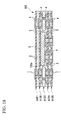
- FIG. 18 is an example of a component-embedded board.
- the component-embedded board 100 includes a double-sided wiring board A103 in which a conductive layer 4 is formed on both faces of an insulation resin layer 3, and single-sided wiring boards A101, A102, A104, and A105 in which the conductive layer 4 are formed on the outer side of the insulation resin layer 3.
- One and the other faces of the double-sided wiring board A103 are provided with the single-sided wiring boards A101, A102, A104, and A105.
- An electric component 2 is embedded in an opening portion 103a of the double-sided wiring board A103.
- the wiring boards A101-A105 are adhered together with an adhesion layer 5 and electrically connected to each other through an interlayer conductive portion 1.
- FIG. 19 and FIG. 20 are a process drawing showing an example of a method of manufacturing a component-embedded board 100.
- the manufacturing method includes: disposing single-sided wiring boards A102 and A104 which are provided with the adhesion layer 5 on one face and the other face of the double-sided wiring board A103, respectively, such that the adhesion layer 5 opposes the double-sided wiring board A103; and collectively laminating them.
- Patent Document 1 Japanese Unexamined Patent Application, First Publication No. 2008-270362
- both faces of the electric component 2 need to be covered by adhesive material (adhesion layer 5) in view of improving the durability.
- adhesive layer 5 adhesive material
- the single-sided wiring boards A102 and A104 are disposed such that their adhesion layers 5 face the inner-layer side (toward wiring board A103).
- the additional single-sided wiring board is also disposed such that its adhesion layer faces the inner-layer side.
- another adhesion layer needs to be provided on a face of the electric component so as to face the inner-layer side.
- the present invention was made in view of the above-described circumstances and the object thereof is providing a component-embedded board and a method of manufacturing the same which enable a reduction of the whole thickness of the component-embedded board incorporating an electric component to be achieved.
- a component-embedded board includes: a first base including a first substrate which incorporates a first electric component, and a first electrode which is provided on a first face of the first substrate and electrically connected to the first electric component; a first adhesion portion provided on the first face of the first substrate; a second electronic component fixed on the first face of the first substrate with the first adhesion portion therebetween; a second base including a second substrate having an opening portion in a position at which the second electronic component is embedded, and a second electrode exposed at a first face of the second substrate; a second adhesion portion arranged between the first base and the second base, and fixing a second face of the second substrate on the first face of the first substrate; a third base including a third substrate and a third electrode which is exposed at a first face of the third substrate; and a third adhesion portion arranged between the second base and the third base, and fixing a second face of the third substrate on the first face of the second substrate, wherein the first electrode, the first electrode which is provided on
- the first base includes an inner-layer base which incorporates the first electric component, a first-side base which faces a first face of the inner-layer base, and a second-side base which faces a second face of the inner-layer base
- the inner-layer base includes an inner-layer substrate which has an opening portion in a position at which the first electric component is embedded, and inner-layer electrodes formed on both faces of the inner-layer substrate
- the first-side base includes a first-side substrate and a first-side electrode formed on a face of the first-side substrate which is opposite to the inner-layer substrate
- the second-side base includes a second-side substrate and a second-side electrode formed on a face of the second-side substrate which is opposite to the inner-layer substrate
- the first-side electrode and the second-side electrode are electrically connected to the inner-layer electrode.
- a component-embedded board is a method of manufacturing the above-described component-embedded board including: arranging the first adhesion portion on the second face of the second substrate; and fixing the second electronic component to the first adhesion portion.
- a component-embedded board according to an aspect of the present invention is a method of manufacturing a component-embedded board according to Claim 1 or 2 including: arranging the first adhesion portion on the first face of the first substrate; and fixing the second electronic component to the first adhesion portion.
- the first adhesion portion and the second adhesion portion are present in the same plane (on the first substrate) when being laminated. For this reason, the total thickness of the adhesion portions covering both faces of the second electronic component can be substantially the same as that of the adhesion portions for laminating the first to third bases.
- the thickness of the adhesion portions can be minimized, and thus a reduction of the whole thickness of the component-embedded board can be achieved.
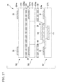
- FIG. 17 is a cross-sectional view schematically showing the structure of a component-embedded board 10 according to a first embodiment of the present invention.
- the component-embedded board 10 includes, at least, a first base B1 including a first substrate 21A, a second electronic component C2 fixed on a face 21Aa of the first substrate 21A via a first adhesion portion 41, a second base B2 being fixed on the face 21Aa of the first substrate 21A via a second adhesion portion 42, and a third base B3 being fixed on a second substrate 22A of the second base B2 via a third adhesion portion 43.
- the first to third substrates 21A-23A may be an insulation resin layer made of, for example, polyimide or the like.
- the first and second electronic components C1 and C2 are, for example, a resistor, capacitor, IC, diode, transistor, semiconductor (bear) chip, or WLCSP.
- the first substrate 21A of the first base B1 incorporates the first electric component C1.
- a first electrode 31 is formed on the first face 21A of the first substrate 21A. The first electrode 31 is exposed at the first face 21Aa of the first substrate 21A and electrically connected to the first electric component C1.
- the second base B2 includes the second substrate 22A, and the second substrate 22A has an opening portion 24 at which the second electronic component C2 is embedded.
- a second electrode 32 is formed on a first face 22Aa of the second substrate 22A so as to be exposed.
- a second face 22Ab of the second substrate 22A is fixed on the first face 21A of the first substrate 21A via the second adhesion portion 42.
- the third base B3 includes a third substrate 23A.
- a third electrode 33 is formed on a first face 23Aa of the third substrate 23A so as to be exposed.
- a second face 23Ab of the third substrate 23A is fixed on the first face 22Aa of the second substrate 22A via the third adhesion portion 43.
- the first electrode 31, the second electrode 32, and the third electrode 33 include a unit for making an electrical connection with the second electronic component C2.
- the first electrode 31, the second electrode 32, and the third electrode 33 may be electrically connected to the second electronic component C2 through an interlayer conductive portion (not shown in the figures) formed so as to penetrate the substrates 22A and 23A in the thickness direction, a conductive layer (not shown in the figures) formed on the faces 21Aa, 22Aa, 22Ab, 23Aa, and 23Ab, or the like.
- the second electronic component C2 is surrounded by the first adhesion portion 41, the second adhesion portion 42, and the third adhesion portion 43.
- the first adhesion portion 41 is on the first substrate 21A as with the second adhesion portion 42. That is, the first adhesion portion 41 and the second adhesion portion 42 are formed in the same plane when being laminated.
- the total thickness of the adhesion portions 41 and 43 covering both faces of the second electronic component C2 can be substantially the same as the total thickness of the adhesion portions 42 and 43 for laminating the first base B1 to the third base B3, the thickness of the adhesion portions can be minimized, and thus a reduction of the whole thickness of the component-embedded board 10 can be achieved.
- a first face refers to an upper-side face and a second face refers to a lower-side face in FIG. 1 .
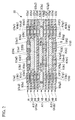
- FIG. 1 is a cross-sectional view showing a component-embedded board 20 according to a second embodiment of the present invention before lamination.
- FIG. 2 is a cross-sectional view showing the component-embedded board 20 after a lamination.
- the component-embedded board 20 is, for example, a laminated printed wiring board with a built-in electric component 2, which includes: a first component substrate A11 (first base) incorporating a first electric component 2 (2B); second and third electric component 2 (2A and 2C) provided on and under (both sides of) the first component substrate A11; an intermediate substrate A12 (A12a and A12b) (second base) provided on and under (both sides of) the first component substrate A11; and first and ninth wiring boards A1 and A9 (third base) provided further outside the intermediate substrate A12 (A12a and A12b), respectively.
- Wiring boards A2-A8 constituting the substrates A11 and A12, and a wiring board body 3 (3a-3i) of the wiring boards A1 and A9 are an insulation resin layer (insulator) made of, for example, polyimide or the like.
- a conductive layer 4 (4a1-4i1) (electrode) of the wiring boards A1-A9 and the electric component 2 (2A-2C) are made of conductive material such as copper.
- the conductive layer 4 may be a wiring layer formed in the wiring boards A1-A9 and the electric components 2A-2C.
- An interlayer conductive portion 1 (1a1-1i1) is formed so as to penetrate, the wiring board body 3 of the wiring boards A1-A9 in the thickness direction.
- the interlayer conductive portion 1 is obtained preferably by heating and curing conductive paste containing metal particles such as nickel, silver, copper, tin, bismuth, indium, and lead.
- conductive paste containing low electric-resistive metal particles such as nickel, silver, and copper as well as low melting point metal particles such as tin, bismuth, indium, and lead.
- adhesion layer 5 (adhesion portion).
- adhesion portion Preferable examples thereof includes polyimide-based adhesive and epoxy-based adhesive.
- the shape and size of an opening portion 6 (6b-6h) of the wiring board body 3 may be determined in accordance with the electric component 2 and the opening portion 6 (6b-6h) may be formed in a position at which the electric component 2 is to be embedded.
- a single-sided copper-clad laminate (CCL) including the wiring board body 3 and a conductive layer provided on the first face of the wiring board body 3 may be employed for the wiring boards A1-A4 and A6-A9.
- a double-sided copper-clad laminate (CCL) including the wiring board body 3 and the conductive layer 4 provided on both faces of the wiring board body 3 may be employed for the fifth wiring board A5.
- the first component substrate A11 includes the fifth wiring board A5 (inner-layer base) incorporating the first electric component 2B, the fourth wiring board A4 (first-side base) facing the first face (upper face in FIG. 1 ) of the fifth wiring board A5, and the sixth wiring board A6 (the second-side base) facing the second face (lower face in FIG. 1 ) of the fifth wiring board A5.
- the fifth wiring board A5 includes the fifth wiring board body 3e (inner-layer substrate) having the opening portion 6e in a position at which the first electric component 2B is to be embedded.
- the inner-layer conductive layer 4e1 (electrode) is formed on a first face 3e1 of the fifth wiring board body 3e.
- the inner-layer conductive layer 4e2 (electrode) is formed on a second face 3e2 of the fifth wiring board body 3e.
- the inner-layer conductive layers 4e1 and 4e2 are connected to each other and electrically connected to the first electric component 2B.
- the fourth wiring board A4 includes the fourth wiring board body 3d (first-side substrate).
- the first-side conductive layer 4d1 (electrode) is formed on a first face 3d1 (upper face) of the fourth wiring board body 3d, and the adhesion layer 5 is formed on a second face 3d2 (lower face).
- the first-side conductive layer 4d1 is electrically connected to the inner-layer conductive layer 4e1 through the interlayer conductive portion 1d1 which penetrates the fourth wiring board body 3d.
- the sixth wiring board A6 includes the sixth wiring board body 3f (second-side substrate), the second-side conductive layer 4f1 (electrode) is formed on a second face 3f2 (lower face) of the sixth wiring board body 3f, and the adhesion layer 5 is formed on a first face 3f1 (upper face).
- Some of the second-side conductive layers 4f1 are electrically connected to the inner-layer conductive layers 4e2 through the interlayer conductive portions 1f1 which penetrate the sixth wiring board body 3f.
- the other of the second-side conductive layers 4f1 are connected to the conductive layers 4k1 (electrode) of the first electric component 2B through the interlayer conductive portions 1f2.
- the first-third electric components 2 (2A-2C) may be a passive component such as resistor and capacitor, or may be an active component such as IC, diode, transistor. In addition, it may be a semiconductor (bare) chip having a semiconductor element or a WLCSP.
- the conductive layer 4k1 is formed on a second face 2B1 (lower face) of the first electric component 2B.
- the first electric component 2B is arranged inside the opening portion 6e of the fifth wiring board A5.
- the intermediate substrate A12 (A12a) includes the second wiring board A2 and the third wiring board A3 facing a second face (lower face) of the second wiring board A2.
- the second wiring board A2 includes the second wiring board body 3b having the opening portion 6b in a position at which the second electric component 2A is to be embedded.
- the second conductive layer 4b1 (electrode) is formed on the first face 3b1 (upper face side) of the second wiring board body 3b, while the adhesion layer 5 is formed on a second face 3b2 (lower face side).
- the second conductive layer 4b1 is electrically connected to the third conductive layer 4c1 through the interlayer conductive portion 1b1 which penetrates the second wiring board body 3b.
- the second conductive layer 4b1 is electrically connected to the second electric component 2A.
- the third wiring board A3 includes the third wiring board body 3c having an opening portion 6c in a position at which the second electric component 2A is to be embedded.
- the third conductive layer 4c1 (electrode) is provided on a first face 3c1 (upper face) of the third wiring board body 3c.
- the third conductive layer 4c1 is electrically connected to the fourth conductive layer 4d1 through the interlayer conductive portion 1c1 which penetrates the third wiring board body 3c.
- the substrate adhesion layer 5 (5c2) (second adhesion portion) is formed on part of a second face 3c2 (lower face side) at which the opening portion 6c of the third wiring board body 3c is not formed.
- the electric component adhesion layer 5 (5c1) (first adhesion portion) is formed on part of the second face (lower face) at which the opening portion 6c is present.
- the substrate adhesion layer 5c2 and the electric component adhesion layer 5c1 are integrally formed with each other and form a flat plate shape having a uniform thickness as a whole.
- the conductive layer 4j1 is formed on a first face 2A1 (upper face) of the second electric component 2A.
- the second electric component 2A is arranged inside the opening portions 6b and 6c of the second wiring board A2 and the third wiring board A3.
- the first wiring board A1 includes the first wiring board body 3a.
- the first conductive layer 4a1 (electrode) is formed on a first face 3a1 (upper face) of the first wiring board body 3a, while the adhesion layer 5 (5a) (third adhesion portion) is formed on a second face 3a2 (lower face).
- first conductive layers 4a1 are electrically connected to the second conductive layers 4b1 through the interlayer conductive portions 1a1 which penetrate the first wiring board body 3a.
- the other of the first conductive layers 4a1 are electrically connected to the conductive layers 4j1 (electrode) of the second electric component 2A through the interlayer conductive portions 1a2.
- the intermediate substrate A12 (A12b) includes the seventh wiring board A7 and the eighth wiring board A8 facing the second face (lower face) of the seventh wiring board A7.
- the seventh wiring board A7 includes the seventh wiring board body 3g having an opening portion 6g in a position at which the third electric component 2C is to be embedded.
- a seventh conductive layer 4g1 (electrode) is formed on a second face 3g2 (lower face side) of the seventh wiring board body 3g.
- the seventh conductive layer 4g1 is electrically connected to the sixth conductive layer 4f1 through the interlayer conductive portion 1g1 which penetrates the seventh wiring board body 3g.
- the substrate adhesion layer 5 (5g2) (second adhesion portion) is formed on part of a first face 3g1 (upper face side) at which the opening portion 6g of the seventh wiring board body 3g is not formed.
- the electric component adhesion layer 5 (5g1) (first adhesion portion) is formed on the first face (upper face) at which the opening portion 6g is present.
- the substrate adhesion layer 5g2 and the electric component adhesion layer 5g1 are integrally formed with each other and form a flat plate shape having a uniform thickness as a whole.
- the eighth wiring board A8 includes the eighth wiring board body 3h having opening portion 6h in a position at which the third electric component 2C is to be embedded.
- the eighth conductive layer 4h1 (electrode) is formed on a second face 3h2 (lower face) of the eighth wiring board body 3h, while the adhesion layer 5 is formed on a first face 3h1 (upper face).
- the eighth conductive layer 4h1 is electrically connected to the seventh conductive layer 4g1 through the interlayer conductive portion 1h1 which penetrates the eighth wiring board body 3h.
- the eighth conductive layer 4h1 is electrically connected to the third electric component 2C.
- the conductive layer 4ml is formed on a second face 2C2 (lower face) of the third electric component 2C.
- the third electric component 2C is arranged within the opening portions 6g and 6h of the seventh wiring board A7 and the eighth wiring board A8.
- the ninth wiring board A9 includes the ninth wiring board body 3i.
- the ninth conductive layer 4i1 (electrode) is formed on a second face 3i2 (lower face) of the ninth wiring board body 3i, while the adhesion layer 5 (5i) (third adhesion portion) is formed on a first face 3i1 (upper face).
- Some of the ninth conductive layers 4i1 are electrically connected to the eighth conductive layers 4h1 through the interlayer conductive portions 1i1 which penetrate the ninth wiring board body 3i.
- the other of the eighth conductive layers 4h1 are connected to the conductive layers 4ml (electrode) of the third electric component 2C through the interlayer conductive portions 1i2 which penetrate the ninth wiring board body 3i.
- the wiring board body 3 (3c and 3g) in which the conductive layer 4 (4c1 and 4g1) is formed on the first face is prepared and the opening portion 6 (6c and 6g) is formed in the wiring board body 3 by laser processing as shown in FIG. 5 .
- an adhesive sheet is laminated on the upper face of the wiring board body 3 (the face facing the conductive layer 4 side) to form the adhesion layer 5.
- Part of the adhesion layer 5 at which the opening portion 6 is absent is the substrate adhesion layer 5 (5c2 and 5g2), while part of the adhesion layer 5 at which the opening portion 6 is present is the electric component adhesion layer 5 (5c1 and 5g1).
- a via 1a is formed in the wiring board body 3 and the adhesion layer 5 by delivering laser beam and performing laser processing and the like.
- the via 1a is filled with conductive paste by screen printing or the like to form the interlayer conductive portion 1, and thereby the wiring board is obtained.
- the first-ninth wiring boards A1-A9 and the electric components 2A-2C shown in FIG. 1 and FIG. 2 are laminated by a collective lamination method while using the wiring board shown in FIG. 8 for the third wiring board A3 and the seventh wiring board A7, and thereby the component-embedded board 20 is obtained.
- the second electric component 2A is embedded in the component-embedded board 20 so as to be covered by the adhesion layer 5a of the first wiring board A1 and the adhesion layers 5c1 and 5c2 of the third wiring board A3.
- the third electric component 2C is embedded in the component-embedded board 20 so as to be covered by the adhesion layer 5i of the ninth wiring board A1 and the adhesion layers 5g1 and 5g2 of the seventh wiring board A7.
- the opening portion 6c capable of housing the second electric component 2A is formed in the third wiring board body 3c of the third wiring board A3.
- the electric component adhesion layer 5c1 of the adhesion layer 5 formed on the second face 3c2 (lower face in FIG. 1 ) of the third wiring board body 3c can abut a second face 2A2 of the second electric component 2A.
- the first face 2A1 of the second electric component 2A is covered by the adhesion layer 5a of the first wiring board A1, while the second face 2A2 is covered by the electric component adhesion layer 5c1 of the third wiring board A3.
- the electric component adhesion layer 5c1 is on the second face 3c2 (lower face) of the third wiring board body 3c as with the substrate adhesion layer 5c2. That is, the electric component adhesion layer 5c1 and the substrate adhesion layer 5c2 are arranged in the same plane.
- the opening portion 6g capable of housing the third electric component 2C is formed in the seventh wiring board body 3g of the seventh wiring board A7.
- the electric component adhesion layer 5g1 of the adhesion layer 5 formed on the first face 3g1 (upper face in FIG. 1 ) of the seventh wiring board body 3g can abut a first face 2C1 of the third electric component 2C.
- the first face 2C1 of the third electric component 2C is covered by the electric component adhesion layer 5g1 of the seventh wiring board A7, while the second face 2C2 is covered by the adhesion layer 5i of the ninth wiring board A9.
- the electric component adhesion layer 5g1 is on the first face 3g1 (upper face) of the seventh wiring board body 3g as with the substrate adhesion layer 5g2. That is, the electric component adhesion layer 5g1 and the substrate adhesion layer 5g2 are arranged in the same plane.
- the total thickness of the adhesion layer 5 (5a, 5c1, 5g1, and 5i) covering the electric components 2A and 2C can be substantially the same as the total thickness of the adhesion layer 5 (5a, 5c2, 5g2, and 5i) for laminating the wiring boards A1, A3, A7, and A9.
- the thickness of the adhesion layer 5 can be minimized, and thus a reduction of the thickness of the component-embedded board 20 can be achieved.
- the wiring board body 3 (3c and 3g) of the wiring boards A3 and A7 is present on the faces 2A2 and 2C1 of the electric components 2A and 2C, which encourages peeling between the electric components 2A and 2C and the wiring board body 3. If another adhesion layer is additionally formed between the wiring board body 3 and the electric component 2 in order to avoid it, the whole thickness will increase.
- the above-described manufacturing method uses the intermediate substrate A12 (A12a) in which the electric component adhesion layer 5c1 is formed on the second face 3c2 of the third wiring board body 3c of the third wiring board A3, and includes a step of adhering and fixing the second electric component 2A to the electric component adhesion layer 5c1. That is, the method includes a step of arranging the electric component adhesion layer 5c1 in the second face 3c2 of the third wiring board body 3c and a step of fixing the second electric component 2A to the electric component adhesion layer 5c1. For this reason, the adhesion layer 5 of the third wiring board A3 as is can serve as an adhesion layer covering the face 2A1 of the electric component 2A.
- FIG. 9-FIG. 15 An example of a component-embedded board 30 and method of manufacturing the same according to a third embodiment of the present invention will be explained with reference to FIG. 9-FIG. 15 .
- the same reference numerals are given to the already-described components and descriptions of those may be omitted.
- the wiring board body 3 (3f) in which the conductive layer 4 is formed on the first face is prepared, the adhesion layer 5 is formed on the upper face (the face facing the conductive layer 4 side) (first face 3f1) of the wiring board body 3 as shown in FIG. 10 .
- the via 1a is formed in the wiring board body 3 and the adhesion layer 5 by laser processing and the like.
- the electric component adhesion layer 5 (5F) is formed on the lower face (the face facing the conductive layer 4) (second face 3f2) of the wiring board body 3.
- the shape, size, position, and the like of the electric component adhesion layer 5F is determined so as to cover the first face 2C1 of the third electric component 2C (refer to FIG. 1 and FIG. 2 ), and not to overlap the adhesion layer 5g of the seventh wiring board A7.
- the interlayer conductive portion 1 is formed on the via 1a, and thereby the sixth wiring board A6 including the electric component adhesion layer 5F is obtained.
- the electric component adhesion layer 5D is formed on the first face 3d1 of the fourth wiring board body 3d.
- the electric component adhesion layer 5D is formed so as to cover the second face 2A2 of the second electric component 2A and not to overlap the adhesion layer 5c of the third wiring board A3.
- the third wiring board A3 and the seventh wiring board A7 are not provided with an electric component adhesion layer (5c1 and 5g1 in FIG. 1 ).
- the adhesion layer 5 may be formed on the wiring board body 3 in advance of forming the opening portion 6 in the wiring board body 3, and then another opening portion may be formed in a region of the adhesion layer 5 opposing the opening portion 6 in the process of forming the opening portion 6 in the wiring board body 3 by laser processing and the like.
- the first-ninth wiring boards A1-A9 and the electric components 2A-2C are laminated by a collective lamination method, and thereby the component-embedded board 30 is obtained.
- the second electric component 2A is embedded in the component-embedded board 30 so as to be covered by the adhesion layer 5a of the first wiring board A1 and the electric component adhesion layer 5D of the fourth wiring board A4.
- the third electric component 2C is embedded in the component-embedded board 30 so as to be covered by the adhesion layer 5i of the ninth wiring board A1 and the electric component adhesion layer 5F of the sixth wiring board A6.
- the component-embedded board 30 includes: a first component substrate A21 (first base) which incorporates the first electric component 2B; the second and third electric components 2A and 2C provided on and under (both sides of) the first component substrate A21; an intermediate substrate A22 (A22a and A22b) (second base) provided on and under (both sides of) the first component substrate A21; and the first and ninth wiring boards A1 and A9 (third base) provided further outside the intermediate substrate A22 (A22a and A22b), respectively.
- the first component substrate A21 includes the wiring boards A4-A6, the intermediate substrate A22 (A22a) includes the wiring boards A1-A3, and the intermediate substrate A22 (A22b) includes the wiring boards A7-A9.
- the electric component adhesion layer 5D is formed on the fourth wiring board A4, the first face 2A1 of the second electric component 2A is covered by the adhesion layer 5a of the first wiring board A1, while the second face 2A2 is covered by the electric component adhesion layer 5D of the fourth wiring board A4. Since the electric component adhesion layer 5D is formed so as not to overlap the adhesion layer 5c of the third wiring board A3, the electric component adhesion layer 5D and the adhesion layer 5c are present in the same plane after a lamination.
- the electric component adhesion layer 5F is formed on the sixth wiring board A6, the first face 2C1 of the third electric component 2C is covered by the electric component adhesion layer 5F of the sixth wiring board A6, while the second face 2C2 is covered by the adhesion layer 5i of the ninth wiring board A9. Since the electric component adhesion layer 5F is formed so as not to overlap the adhesion layer 5g of the seventh wiring board A7, the electric component adhesion layer 5F and the adhesion layer 5g are present in the same plane after a lamination.
- the total thickness of the adhesion layer 5 (5a, 5D, 5F, and 5i) covering the electric components 2A and 2C can be substantially the same as the total thickness of the adhesion layer 5 for laminating the wiring boards A1, A3, A7, and A9.
- the thickness of the adhesion layer 5 can be minimized, and thus a reduction of the thickness of the component-embedded board 30 can be achieved.
- the above-described manufacturing method uses the first component substrate A21 in which the electric component adhesion layers 5D and 5F are formed on the wiring boards A4 and A6, and includes a step of adhering and fixing the electric components 2A and 2C to the adhesion layers 5F and 5D. That is, the method includes a step of arranging the electric component adhesion layer 5D on the first face 3d1 of the fourth wiring board body 3d and a step of adhering and fixing the electric component 2A to the adhesion layer 5D.
- the method includes a step of arranging the electric component adhesion layer 5F on the second face 3f2 of the fourth wiring board body 3f and a step of adhering and fixing the electric component 2C to the adhesion layer 5F. For this reason, even in a case where the size of the opening portion 6 (6c, 6g) is large, breakage of the electric component adhesion layers 5D and 5F does not occur, and thus the faces 2A2 and 2C1 of the electric components 2A and 2C can be reliably covered by the adhesion layer 5.
- the component-embedded boards 20 and 30 shown in FIG. 1 , FIG. 2 , FIG. 14 , and FIG. 15 include: the first component substrate (first base); the electric components and the intermediate substrates (second base) each provided on both sides of the first component substrate; and the wiring board (third base) provided further outside each intermediate substrate.
- first base the first component substrate
- second base the electric components and the intermediate substrates
- third base the wiring board
- FIG. 16 is a cross-sectional view showing a component-embedded board 40 according to a fourth embodiment of the present invention.
- the component-embedded board 40 includes: a first component substrate A41 (first base) incorporating the first electric component 2A; the second electric component 2B provided on the lower side of the first component substrate A41; an intermediate substrate A42a (second base) provided on the lower side of the first component substrate A41 and incorporating the second electric component 2B; a sixth wiring board A36 (third base) provided on the lower side of the intermediate substrate A42a; an intermediate substrate A42b (second base) provided on the lower side of the sixth wiring board A36 and incorporating the third electric component 2C; and a ninth wiring board A39(third base) provided on the lower side of the intermediate substrate A42b.
- the first component substrate A41 includes: a second wiring board A32 (inner-layer base) incorporating the first electric component 2A; a first wiring board A31 (first-side base) facing the first face (upper face) of the second wiring board A32; and a third wiring board A33 (second-side base) facing the second face (lower face) of the second wiring board A32.
- the second wiring board A32 is a double-sided wiring board in which the conductive layer 4 is provided on both faces of the second wiring board body 3b (inner-layer substrate) having the opening portion 6 in a position at which the first electric component 2A is embedded.
- the first and third wiring boards A31 and A33 are a single-sided wiring board in which the conductive layer 4 (first-side electrode and second-side electrode) is provided only on the outer face of the first and third wiring board bodies 3a (first-side substrate) and 3c (second-side substrate).
- the intermediate substrate A42a includes a fourth wiring board A34 and a fifth wiring board A35 facing the second face (lower face side) of the fourth wiring board A4.
- the fourth and fifth wiring boards A34 and A35 include the wiring board bodies 3d and 3e having the opening portion 6 in a position at which the second electric component 2B is embedded, and the conductive layer 4 is formed on the second face (lower face) of the wiring board bodies 3d and 3e.
- the sixth wiring board A36 includes the sixth wiring board body 3f, and the conductive layer 4 is formed on the second face (lower face) of the sixth wiring board body 3f.
- the intermediate substrate A42b includes a seventh wiring board A3 7 and a eighth wiring board A38 facing the second face (lower face) of the seventh wiring board A37.
- the seventh and eighth wiring boards A37 and A38 include the wiring board bodies 3g and 3h having the opening portion 6 in a position at which the third electric component 2C is embedded, and the conductive layer 4 is formed on the second face (lower face) of the wiring board bodies 3g and 3h.
- the ninth wiring board A39 includes the ninth wiring board body 3i, and the conductive layer 4 is formed on the second face (lower face) of the ninth wiring board body 3i.
- the component-embedded board 40 includes the electric component adhesion layer 5 facing the first face (upper face) of the wiring boards A34 and A37 as with the component-embedded board 20 (refer to FIG. 1 ) (e.g., seventh wiring board A7), or includes the electric component adhesion layer 5 facing the second face (lower face) of the wiring boards A33 and A36 as with the component-embedded board 30 (refer to FIG. 14 ) (e.g., sixth wiring board A6); and thereby both faces of the electric components 2B and 2C can be covered by the adhesion layer 5.
- the total thickness of the adhesion layer 5 covering the electric components 2B and 2C can be minimized, and thus a reduction of the thickness of the component-embedded board 40 can be achieved.
Landscapes
- Engineering & Computer Science (AREA)
- Manufacturing & Machinery (AREA)
- Microelectronics & Electronic Packaging (AREA)
- Mechanical Engineering (AREA)
- Production Of Multi-Layered Print Wiring Board (AREA)
Description
- The present invention relates to a component-embedded board incorporating an electric component and a method of manufacturing the same.
- Priority is claimed on Japanese Patent Application No.
2011-181544, filed August 23, 2011 - Miniaturization and high functionality of electric equipment has been achieved as well as miniaturization of electronic components incorporated in equipment. Even for a printed wiring board for mounting electric components, higher density, multilayer, multi-layering, and enhancement of high-speed transmission characteristics are required. As a technology to meet these requirements, there is a packaging technology called EWLP (Embedded Wafer Level Package). EWLP is a technology for mounting semiconductor components (electric component) such as a WLCSP (Wafer Level Chip Size Package) to a printed wiring board. According to EWLP, it is possible to improve the packaging density, reduce the wiring length between the semiconductor elements, and enhance the high-speed transmission characteristics.
- A component-embedded board is known in which an electric component is embedded in a double-sided wiring board and a single-sided wiring board is laminated on both sides thereof (see Patent Document 1).
-
FIG. 18 is an example of a component-embedded board. The component-embeddedboard 100 includes a double-sided wiring board A103 in which aconductive layer 4 is formed on both faces of aninsulation resin layer 3, and single-sided wiring boards A101, A102, A104, and A105 in which theconductive layer 4 are formed on the outer side of theinsulation resin layer 3. One and the other faces of the double-sided wiring board A103 are provided with the single-sided wiring boards A101, A102, A104, and A105. Anelectric component 2 is embedded in anopening portion 103a of the double-sided wiring board A103. - The wiring boards A101-A105 are adhered together with an
adhesion layer 5 and electrically connected to each other through an interlayerconductive portion 1. -
FIG. 19 andFIG. 20 are a process drawing showing an example of a method of manufacturing a component-embeddedboard 100. The manufacturing method includes: disposing single-sided wiring boards A102 and A104 which are provided with theadhesion layer 5 on one face and the other face of the double-sided wiring board A103, respectively, such that theadhesion layer 5 opposes the double-sided wiring board A103; and collectively laminating them. - [Patent Document 1] Japanese Unexamined Patent Application, First Publication No.
2008-270362 - In the component-embedded
board 100, both faces of theelectric component 2 need to be covered by adhesive material (adhesion layer 5) in view of improving the durability. For this reason, the single-sided wiring boards A102 and A104 are disposed such that theiradhesion layers 5 face the inner-layer side (toward wiring board A103). - When another single-sided wiring board is added at the outer-layer side of the single-sided wiring boards A102 and A104, the additional single-sided wiring board is also disposed such that its adhesion layer faces the inner-layer side. In this structure, when an electric component needs to be embedded in the additional single-sided wiring board as well, another adhesion layer needs to be provided on a face of the electric component so as to face the inner-layer side.
- However, when such an additional adhesion layer is formed, the total thickness of the adhesion layer will increase, which causes a problem in that the whole thickness of the component-embedded board will increase.
- The present invention was made in view of the above-described circumstances and the object thereof is providing a component-embedded board and a method of manufacturing the same which enable a reduction of the whole thickness of the component-embedded board incorporating an electric component to be achieved.
- A component-embedded board according to an aspect of the present invention includes: a first base including a first substrate which incorporates a first electric component, and a first electrode which is provided on a first face of the first substrate and electrically connected to the first electric component; a first adhesion portion provided on the first face of the first substrate; a second electronic component fixed on the first face of the first substrate with the first adhesion portion therebetween; a second base including a second substrate having an opening portion in a position at which the second electronic component is embedded, and a second electrode exposed at a first face of the second substrate; a second adhesion portion arranged between the first base and the second base, and fixing a second face of the second substrate on the first face of the first substrate; a third base including a third substrate and a third electrode which is exposed at a first face of the third substrate; and a third adhesion portion arranged between the second base and the third base, and fixing a second face of the third substrate on the first face of the second substrate, wherein the first electrode, the second electrode, and the third electrode are electrically connected to the second electronic component, and the second electronic component is surrounded, at least, by the first adhesion portion and the third adhesion portion.
- It may be arranged such that the first base includes an inner-layer base which incorporates the first electric component, a first-side base which faces a first face of the inner-layer base, and a second-side base which faces a second face of the inner-layer base, the inner-layer base includes an inner-layer substrate which has an opening portion in a position at which the first electric component is embedded, and inner-layer electrodes formed on both faces of the inner-layer substrate, the first-side base includes a first-side substrate and a first-side electrode formed on a face of the first-side substrate which is opposite to the inner-layer substrate, the second-side base includes a second-side substrate and a second-side electrode formed on a face of the second-side substrate which is opposite to the inner-layer substrate, and the first-side electrode and the second-side electrode are electrically connected to the inner-layer electrode.
- It may be arranged such that the second electronic component is surrounded by the first adhesion portion, the second adhesion portion, and the third adhesion portion.
- A component-embedded board according to an aspect of the present invention is a method of manufacturing the above-described component-embedded board including: arranging the first adhesion portion on the second face of the second substrate; and fixing the second electronic component to the first adhesion portion.
- A component-embedded board according to an aspect of the present invention is a method of manufacturing a component-embedded board according to
Claim - Based on the above-described aspects of the present invention, since the second electronic component embedded in the opening portion of the second base is fixed to the first base via the first adhesion portion, both faces of the second electronic component are covered by the first adhesion portion and the third adhesion portion, respectively.
- The first adhesion portion and the second adhesion portion are present in the same plane (on the first substrate) when being laminated. For this reason, the total thickness of the adhesion portions covering both faces of the second electronic component can be substantially the same as that of the adhesion portions for laminating the first to third bases.
- Accordingly, the thickness of the adhesion portions can be minimized, and thus a reduction of the whole thickness of the component-embedded board can be achieved.
-
-
FIG. 1 is a cross-sectional view showing a component-embedded board according to the second embodiment of the present invention before lamination. -
FIG. 2 is a cross-sectional view showing a component-embedded board obtained by laminating the substrates shown inFIG. 1 . -
FIG. 3 is a cross-sectional view showing a component-embedded board in which an opening portion is not formed in a third wiring board and a seventh wiring board. -
FIG. 4 is a process drawing showing an example of a method of manufacturing a component-embedded board shown inFIG. 2 . -
FIG. 5 is a process drawing following the previous figure. -
FIG. 6 is a process drawing following the previous figure. -
FIG. 7 is a process drawing following the previous figure. -
FIG. 8 is a process drawing following the previous figure. -
FIG. 9 is a process drawing showing an example of a method of manufacturing a component-embedded board according to the third embodiment of the present invention. -
FIG. 10 is a process drawing following the previous figure. -
FIG. 11 is a process drawing following the previous figure. -
FIG. 12 is a process drawing following the previous figure. -
FIG. 13 is a process drawing following the previous figure. -
FIG. 14 is a process drawing following the previous figure. -
FIG. 15 is a process drawing following the previous figure. -
FIG. 16 is a process drawing following the previous figure. -
FIG. 17 is a cross-sectional view schematically showing the structure of a component-embedded board according to the first embodiment of the present invention. -
FIG. 18 is a cross-sectional view showing an example of a conventional component-embedded board. -
FIG. 19 is a process drawing showing an example of a method of manufacturing a conventional component-embedded board. -
FIG. 20 is a process drawing following the previous figure. - Embodiments of the present invention will be described with reference to the drawings.
-
FIG. 17 is a cross-sectional view schematically showing the structure of a component-embeddedboard 10 according to a first embodiment of the present invention. - The component-embedded
board 10 includes, at least, a first base B1 including afirst substrate 21A, a second electronic component C2 fixed on a face 21Aa of thefirst substrate 21A via afirst adhesion portion 41, a second base B2 being fixed on the face 21Aa of thefirst substrate 21A via asecond adhesion portion 42, and a third base B3 being fixed on asecond substrate 22A of the second base B2 via athird adhesion portion 43. - The first to
third substrates 21A-23A may be an insulation resin layer made of, for example, polyimide or the like. - The first and second electronic components C1 and C2 are, for example, a resistor, capacitor, IC, diode, transistor, semiconductor (bear) chip, or WLCSP.
- The
first substrate 21A of the first base B1 incorporates the first electric component C1. Afirst electrode 31 is formed on thefirst face 21A of thefirst substrate 21A. Thefirst electrode 31 is exposed at the first face 21Aa of thefirst substrate 21A and electrically connected to the first electric component C1. - The second base B2 includes the
second substrate 22A, and thesecond substrate 22A has an openingportion 24 at which the second electronic component C2 is embedded. Asecond electrode 32 is formed on a first face 22Aa of thesecond substrate 22A so as to be exposed. A second face 22Ab of thesecond substrate 22A is fixed on thefirst face 21A of thefirst substrate 21A via thesecond adhesion portion 42. - The third base B3 includes a
third substrate 23A. Athird electrode 33 is formed on a first face 23Aa of thethird substrate 23A so as to be exposed. A second face 23Ab of thethird substrate 23A is fixed on the first face 22Aa of thesecond substrate 22A via thethird adhesion portion 43. - The
first electrode 31, thesecond electrode 32, and thethird electrode 33 include a unit for making an electrical connection with the second electronic component C2. For example, thefirst electrode 31, thesecond electrode 32, and thethird electrode 33 may be electrically connected to the second electronic component C2 through an interlayer conductive portion (not shown in the figures) formed so as to penetrate thesubstrates - The second electronic component C2 is surrounded by the
first adhesion portion 41, thesecond adhesion portion 42, and thethird adhesion portion 43. - In the component-embedded
board 10, since the second electronic component C2 embedded in the openingportion 24 of the second base B2 is fixed to the first base B1 via thefirst adhesion portion 41, both faces of the second electronic component C2 are covered by thefirst adhesion portion 41 and thethird adhesion portion 43 of the third base B3. - The
first adhesion portion 41 is on thefirst substrate 21A as with thesecond adhesion portion 42. That is, thefirst adhesion portion 41 and thesecond adhesion portion 42 are formed in the same plane when being laminated. - Accordingly, the total thickness of the
adhesion portions adhesion portions board 10 can be achieved. - Next, embodiments of the present invention will be explained referring further specific examples. In the description below, unless otherwise specified, a first face refers to an upper-side face and a second face refers to a lower-side face in
FIG. 1 . -
FIG. 1 is a cross-sectional view showing a component-embeddedboard 20 according to a second embodiment of the present invention before lamination.FIG. 2 is a cross-sectional view showing the component-embeddedboard 20 after a lamination. - As shown in
FIG. 1 andFIG. 2 , the component-embeddedboard 20 is, for example, a laminated printed wiring board with a built-inelectric component 2, which includes: a first component substrate A11 (first base) incorporating a first electric component 2 (2B); second and third electric component 2 (2A and 2C) provided on and under (both sides of) the first component substrate A11; an intermediate substrate A12 (A12a and A12b) (second base) provided on and under (both sides of) the first component substrate A11; and first and ninth wiring boards A1 and A9 (third base) provided further outside the intermediate substrate A12 (A12a and A12b), respectively. - Wiring boards A2-A8 constituting the substrates A11 and A12, and a wiring board body 3 (3a-3i) of the wiring boards A1 and A9 are an insulation resin layer (insulator) made of, for example, polyimide or the like. A conductive layer 4 (4a1-4i1) (electrode) of the wiring boards A1-A9 and the electric component 2 (2A-2C) are made of conductive material such as copper. The
conductive layer 4 may be a wiring layer formed in the wiring boards A1-A9 and theelectric components 2A-2C. - An interlayer conductive portion 1 (1a1-1i1) is formed so as to penetrate, the
wiring board body 3 of the wiring boards A1-A9 in the thickness direction. The interlayerconductive portion 1 is obtained preferably by heating and curing conductive paste containing metal particles such as nickel, silver, copper, tin, bismuth, indium, and lead. Alternatively, conductive paste containing low electric-resistive metal particles such as nickel, silver, and copper as well as low melting point metal particles such as tin, bismuth, indium, and lead. - A wide variety of know adhesives in the manufacturing domain of printed wiring boards may be employed for the adhesion layer 5 (5a-5i) (adhesion portion). Preferable examples thereof includes polyimide-based adhesive and epoxy-based adhesive.
- The shape and size of an opening portion 6 (6b-6h) of the
wiring board body 3 may be determined in accordance with theelectric component 2 and the opening portion 6 (6b-6h) may be formed in a position at which theelectric component 2 is to be embedded. - A single-sided copper-clad laminate (CCL) including the
wiring board body 3 and a conductive layer provided on the first face of thewiring board body 3 may be employed for the wiring boards A1-A4 and A6-A9. A double-sided copper-clad laminate (CCL) including thewiring board body 3 and theconductive layer 4 provided on both faces of thewiring board body 3 may be employed for the fifth wiring board A5. - The first component substrate A11 includes the fifth wiring board A5 (inner-layer base) incorporating the first
electric component 2B, the fourth wiring board A4 (first-side base) facing the first face (upper face inFIG. 1 ) of the fifth wiring board A5, and the sixth wiring board A6 (the second-side base) facing the second face (lower face inFIG. 1 ) of the fifth wiring board A5. - The fifth wiring board A5 includes the fifth
wiring board body 3e (inner-layer substrate) having the openingportion 6e in a position at which the firstelectric component 2B is to be embedded. The inner-layer conductive layer 4e1 (electrode) is formed on a first face 3e1 of the fifthwiring board body 3e. The inner-layer conductive layer 4e2 (electrode) is formed on a second face 3e2 of the fifthwiring board body 3e. The inner-layer conductive layers 4e1 and 4e2 are connected to each other and electrically connected to the firstelectric component 2B. - The fourth wiring board A4 includes the fourth
wiring board body 3d (first-side substrate). The first-side conductive layer 4d1 (electrode) is formed on a first face 3d1 (upper face) of the fourthwiring board body 3d, and theadhesion layer 5 is formed on a second face 3d2 (lower face). - The first-side conductive layer 4d1 is electrically connected to the inner-layer conductive layer 4e1 through the interlayer conductive portion 1d1 which penetrates the fourth
wiring board body 3d. - The sixth wiring board A6 includes the sixth
wiring board body 3f (second-side substrate), the second-side conductive layer 4f1 (electrode) is formed on a second face 3f2 (lower face) of the sixthwiring board body 3f, and theadhesion layer 5 is formed on a first face 3f1 (upper face). - Some of the second-side conductive layers 4f1 are electrically connected to the inner-layer conductive layers 4e2 through the interlayer conductive portions 1f1 which penetrate the sixth
wiring board body 3f. The other of the second-side conductive layers 4f1 are connected to the conductive layers 4k1 (electrode) of the firstelectric component 2B through the interlayer conductive portions 1f2. - The first-third electric components 2 (2A-2C) may be a passive component such as resistor and capacitor, or may be an active component such as IC, diode, transistor. In addition, it may be a semiconductor (bare) chip having a semiconductor element or a WLCSP.
- The conductive layer 4k1 is formed on a second face 2B1 (lower face) of the first
electric component 2B. The firstelectric component 2B is arranged inside theopening portion 6e of the fifth wiring board A5. - The intermediate substrate A12 (A12a) includes the second wiring board A2 and the third wiring board A3 facing a second face (lower face) of the second wiring board A2.
- The second wiring board A2 includes the second
wiring board body 3b having the openingportion 6b in a position at which the secondelectric component 2A is to be embedded. The second conductive layer 4b1 (electrode) is formed on the first face 3b1 (upper face side) of the secondwiring board body 3b, while theadhesion layer 5 is formed on a second face 3b2 (lower face side). - The second conductive layer 4b1 is electrically connected to the third conductive layer 4c1 through the interlayer conductive portion 1b1 which penetrates the second
wiring board body 3b. In addition, the second conductive layer 4b1 is electrically connected to the secondelectric component 2A. - The third wiring board A3 includes the third
wiring board body 3c having an openingportion 6c in a position at which the secondelectric component 2A is to be embedded. The third conductive layer 4c1 (electrode) is provided on a first face 3c1 (upper face) of the thirdwiring board body 3c. - The third conductive layer 4c1 is electrically connected to the fourth conductive layer 4d1 through the interlayer conductive portion 1c1 which penetrates the third
wiring board body 3c. - The substrate adhesion layer 5 (5c2) (second adhesion portion) is formed on part of a second face 3c2 (lower face side) at which the
opening portion 6c of the thirdwiring board body 3c is not formed. The electric component adhesion layer 5 (5c1) (first adhesion portion) is formed on part of the second face (lower face) at which theopening portion 6c is present. - The substrate adhesion layer 5c2 and the electric component adhesion layer 5c1 are integrally formed with each other and form a flat plate shape having a uniform thickness as a whole.
- The conductive layer 4j1 is formed on a first face 2A1 (upper face) of the second
electric component 2A. The secondelectric component 2A is arranged inside the openingportions - The first wiring board A1 includes the first
wiring board body 3a. The first conductive layer 4a1 (electrode) is formed on a first face 3a1 (upper face) of the firstwiring board body 3a, while the adhesion layer 5 (5a) (third adhesion portion) is formed on a second face 3a2 (lower face). - Some of the first conductive layers 4a1 are electrically connected to the second conductive layers 4b1 through the interlayer conductive portions 1a1 which penetrate the first
wiring board body 3a. The other of the first conductive layers 4a1 are electrically connected to the conductive layers 4j1 (electrode) of the secondelectric component 2A through the interlayer conductive portions 1a2. - The intermediate substrate A12 (A12b) includes the seventh wiring board A7 and the eighth wiring board A8 facing the second face (lower face) of the seventh wiring board A7.
- The seventh wiring board A7 includes the seventh
wiring board body 3g having an openingportion 6g in a position at which the thirdelectric component 2C is to be embedded. A seventh conductive layer 4g1 (electrode) is formed on a second face 3g2 (lower face side) of the seventhwiring board body 3g. - The seventh conductive layer 4g1 is electrically connected to the sixth conductive layer 4f1 through the interlayer conductive portion 1g1 which penetrates the seventh
wiring board body 3g. - The substrate adhesion layer 5 (5g2) (second adhesion portion) is formed on part of a first face 3g1 (upper face side) at which the
opening portion 6g of the seventhwiring board body 3g is not formed. The electric component adhesion layer 5 (5g1) (first adhesion portion) is formed on the first face (upper face) at which theopening portion 6g is present. - The substrate adhesion layer 5g2 and the electric component adhesion layer 5g1 are integrally formed with each other and form a flat plate shape having a uniform thickness as a whole.
- The eighth wiring board A8 includes the eighth
wiring board body 3h havingopening portion 6h in a position at which the thirdelectric component 2C is to be embedded. - The eighth conductive layer 4h1 (electrode) is formed on a second face 3h2 (lower face) of the eighth
wiring board body 3h, while theadhesion layer 5 is formed on a first face 3h1 (upper face). - The eighth conductive layer 4h1 is electrically connected to the seventh conductive layer 4g1 through the interlayer conductive portion 1h1 which penetrates the eighth
wiring board body 3h. In addition, the eighth conductive layer 4h1 is electrically connected to the thirdelectric component 2C. - The conductive layer 4mlis formed on a second face 2C2 (lower face) of the third
electric component 2C. The thirdelectric component 2C is arranged within the openingportions - The ninth wiring board A9 includes the ninth
wiring board body 3i. The ninth conductive layer 4i1 (electrode) is formed on a second face 3i2 (lower face) of the ninthwiring board body 3i, while the adhesion layer 5 (5i) (third adhesion portion) is formed on a first face 3i1 (upper face). - Some of the ninth conductive layers 4i1 are electrically connected to the eighth conductive layers 4h1 through the interlayer conductive portions 1i1 which penetrate the ninth
wiring board body 3i. The other of the eighth conductive layers 4h1 are connected to the conductive layers 4ml (electrode) of the thirdelectric component 2C through the interlayer conductive portions 1i2 which penetrate the ninthwiring board body 3i. - Next, an example of a method of manufacturing the component-embedded
board 20 will be explained with reference toFIG. 4-FIG. 8 . - As shown in
FIG. 4 , the wiring board body 3 (3c and 3g) in which the conductive layer 4 (4c1 and 4g1) is formed on the first face is prepared and the opening portion 6 (6c and 6g) is formed in thewiring board body 3 by laser processing as shown inFIG. 5 . - Then, as shown in
FIG. 6 , an adhesive sheet is laminated on the upper face of the wiring board body 3 (the face facing theconductive layer 4 side) to form theadhesion layer 5. Part of theadhesion layer 5 at which theopening portion 6 is absent is the substrate adhesion layer 5 (5c2 and 5g2), while part of theadhesion layer 5 at which theopening portion 6 is present is the electric component adhesion layer 5 (5c1 and 5g1). - After that, a via 1a is formed in the
wiring board body 3 and theadhesion layer 5 by delivering laser beam and performing laser processing and the like. - As shown in
FIG. 9 , the via 1a is filled with conductive paste by screen printing or the like to form the interlayerconductive portion 1, and thereby the wiring board is obtained. - The first-ninth wiring boards A1-A9 and the
electric components 2A-2C shown inFIG. 1 andFIG. 2 are laminated by a collective lamination method while using the wiring board shown inFIG. 8 for the third wiring board A3 and the seventh wiring board A7, and thereby the component-embeddedboard 20 is obtained. - The second
electric component 2A is embedded in the component-embeddedboard 20 so as to be covered by theadhesion layer 5a of the first wiring board A1 and the adhesion layers 5c1 and 5c2 of the third wiring board A3. - The third
electric component 2C is embedded in the component-embeddedboard 20 so as to be covered by theadhesion layer 5i of the ninth wiring board A1 and the adhesion layers 5g1 and 5g2 of the seventh wiring board A7. - As shown in
FIG. 1 andFIG. 2 , in the component-embeddedboard 20, the openingportion 6c capable of housing the secondelectric component 2A is formed in the thirdwiring board body 3c of the third wiring board A3. For this reason, the electric component adhesion layer 5c1 of theadhesion layer 5 formed on the second face 3c2 (lower face inFIG. 1 ) of the thirdwiring board body 3c can abut a second face 2A2 of the secondelectric component 2A. - As a result, the first face 2A1 of the second
electric component 2A is covered by theadhesion layer 5a of the first wiring board A1, while the second face 2A2 is covered by the electric component adhesion layer 5c1 of the third wiring board A3. - The electric component adhesion layer 5c1 is on the second face 3c2 (lower face) of the third
wiring board body 3c as with the substrate adhesion layer 5c2. That is, the electric component adhesion layer 5c1 and the substrate adhesion layer 5c2 are arranged in the same plane. - Similarly, the opening
portion 6g capable of housing the thirdelectric component 2C is formed in the seventhwiring board body 3g of the seventh wiring board A7. For this reason, the electric component adhesion layer 5g1 of theadhesion layer 5 formed on the first face 3g1 (upper face inFIG. 1 ) of the seventhwiring board body 3g can abut a first face 2C1 of the thirdelectric component 2C. - As a result, the first face 2C1 of the third
electric component 2C is covered by the electric component adhesion layer 5g1 of the seventh wiring board A7, while the second face 2C2 is covered by theadhesion layer 5i of the ninth wiring board A9. - The electric component adhesion layer 5g1 is on the first face 3g1 (upper face) of the seventh
wiring board body 3g as with the substrate adhesion layer 5g2. That is, the electric component adhesion layer 5g1 and the substrate adhesion layer 5g2 are arranged in the same plane. - Therefore, the total thickness of the adhesion layer 5 (5a, 5c1, 5g1, and 5i) covering the
electric components adhesion layer 5 can be minimized, and thus a reduction of the thickness of the component-embeddedboard 20 can be achieved. - In contrast, as shown in
FIG. 3 , in the component-embedded board in which the opening portion is not formed in the third wiring board A3 or the seventh wiring board A7, the wiring board body 3 (3c and 3g) of the wiring boards A3 and A7 is present on the faces 2A2 and 2C1 of theelectric components electric components wiring board body 3. If another adhesion layer is additionally formed between thewiring board body 3 and theelectric component 2 in order to avoid it, the whole thickness will increase. - On the other hand, the above-described manufacturing method (refer to
FIG. 4-FIG. 8 ) uses the intermediate substrate A12 (A12a) in which the electric component adhesion layer 5c1 is formed on the second face 3c2 of the thirdwiring board body 3c of the third wiring board A3, and includes a step of adhering and fixing the secondelectric component 2A to the electric component adhesion layer 5c1. That is, the method includes a step of arranging the electric component adhesion layer 5c1 in the second face 3c2 of the thirdwiring board body 3c and a step of fixing the secondelectric component 2A to the electric component adhesion layer 5c1. For this reason, theadhesion layer 5 of the third wiring board A3 as is can serve as an adhesion layer covering the face 2A1 of theelectric component 2A. - Accordingly, without additionally forming another adhesion layer, it is possible to simplify the manufacturing process and enhance the manufacturing efficiency.
- Next, an example of a component-embedded
board 30 and method of manufacturing the same according to a third embodiment of the present invention will be explained with reference toFIG. 9-FIG. 15 . In the following descriptions, the same reference numerals are given to the already-described components and descriptions of those may be omitted. - As shown in
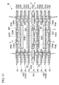
FIG. 9 , the wiring board body 3 (3f) in which theconductive layer 4 is formed on the first face is prepared, theadhesion layer 5 is formed on the upper face (the face facing theconductive layer 4 side) (first face 3f1) of thewiring board body 3 as shown inFIG. 10 . - Then, as shown in
FIG. 11 , the via 1a is formed in thewiring board body 3 and theadhesion layer 5 by laser processing and the like. - After that, as shown in
FIG. 12 , the electric component adhesion layer 5 (5F) is formed on the lower face (the face facing the conductive layer 4) (second face 3f2) of thewiring board body 3. The shape, size, position, and the like of the electriccomponent adhesion layer 5F is determined so as to cover the first face 2C1 of the thirdelectric component 2C (refer toFIG. 1 andFIG. 2 ), and not to overlap theadhesion layer 5g of the seventh wiring board A7. - As shown in
FIG. 13 , the interlayerconductive portion 1 is formed on the via 1a, and thereby the sixth wiring board A6 including the electriccomponent adhesion layer 5F is obtained. - As shown in
FIG. 14 , in the fourth wiring board A4, the electriccomponent adhesion layer 5D is formed on the first face 3d1 of the fourthwiring board body 3d. The electriccomponent adhesion layer 5D is formed so as to cover the second face 2A2 of the secondelectric component 2A and not to overlap the adhesion layer 5c of the third wiring board A3. - In contrast to the wiring boards A3 and A7 of the component-embedded
board 20 shown inFIG. 1 , the third wiring board A3 and the seventh wiring board A7 are not provided with an electric component adhesion layer (5c1 and 5g1 inFIG. 1 ). - When manufacturing the wiring boards A3 and A7 without an electric component adhesion layer, the
adhesion layer 5 may be formed on thewiring board body 3 in advance of forming theopening portion 6 in thewiring board body 3, and then another opening portion may be formed in a region of theadhesion layer 5 opposing theopening portion 6 in the process of forming theopening portion 6 in thewiring board body 3 by laser processing and the like. - As shown in
FIG. 14 andFIG. 15 , the first-ninth wiring boards A1-A9 and theelectric components 2A-2C are laminated by a collective lamination method, and thereby the component-embeddedboard 30 is obtained. - The second
electric component 2A is embedded in the component-embeddedboard 30 so as to be covered by theadhesion layer 5a of the first wiring board A1 and the electriccomponent adhesion layer 5D of the fourth wiring board A4. - The third
electric component 2C is embedded in the component-embeddedboard 30 so as to be covered by theadhesion layer 5i of the ninth wiring board A1 and the electriccomponent adhesion layer 5F of the sixth wiring board A6. - The component-embedded
board 30 includes: a first component substrate A21 (first base) which incorporates the firstelectric component 2B; the second and thirdelectric components - The first component substrate A21 includes the wiring boards A4-A6, the intermediate substrate A22 (A22a) includes the wiring boards A1-A3, and the intermediate substrate A22 (A22b) includes the wiring boards A7-A9.
- In the component-embedded board 30 (refer to
FIG. 14 andFIG. 15 ), since the electriccomponent adhesion layer 5D is formed on the fourth wiring board A4, the first face 2A1 of the secondelectric component 2A is covered by theadhesion layer 5a of the first wiring board A1, while the second face 2A2 is covered by the electriccomponent adhesion layer 5D of the fourth wiring board A4. Since the electriccomponent adhesion layer 5D is formed so as not to overlap the adhesion layer 5c of the third wiring board A3, the electriccomponent adhesion layer 5D and the adhesion layer 5c are present in the same plane after a lamination. - Similarly, since the electric
component adhesion layer 5F is formed on the sixth wiring board A6, the first face 2C1 of the thirdelectric component 2C is covered by the electriccomponent adhesion layer 5F of the sixth wiring board A6, while the second face 2C2 is covered by theadhesion layer 5i of the ninth wiring board A9. Since the electriccomponent adhesion layer 5F is formed so as not to overlap theadhesion layer 5g of the seventh wiring board A7, the electriccomponent adhesion layer 5F and theadhesion layer 5g are present in the same plane after a lamination. - Accordingly, the total thickness of the adhesion layer 5 (5a, 5D, 5F, and 5i) covering the
electric components adhesion layer 5 for laminating the wiring boards A1, A3, A7, and A9. As a result, the thickness of theadhesion layer 5 can be minimized, and thus a reduction of the thickness of the component-embeddedboard 30 can be achieved. - In addition, the above-described manufacturing method (refer to
FIG. 9-FIG. 15 ) uses the first component substrate A21 in which the electric component adhesion layers 5D and 5F are formed on the wiring boards A4 and A6, and includes a step of adhering and fixing theelectric components component adhesion layer 5D on the first face 3d1 of the fourthwiring board body 3d and a step of adhering and fixing theelectric component 2A to theadhesion layer 5D. In addition, the method includes a step of arranging the electriccomponent adhesion layer 5F on the second face 3f2 of the fourthwiring board body 3f and a step of adhering and fixing theelectric component 2C to theadhesion layer 5F. For this reason, even in a case where the size of the opening portion 6 (6c, 6g) is large, breakage of the electric component adhesion layers 5D and 5F does not occur, and thus the faces 2A2 and 2C1 of theelectric components adhesion layer 5. - The component-embedded
boards FIG. 1 ,FIG. 2 ,FIG. 14 , andFIG. 15 include: the first component substrate (first base); the electric components and the intermediate substrates (second base) each provided on both sides of the first component substrate; and the wiring board (third base) provided further outside each intermediate substrate. However, the present invention is not limited to this, and only either side of the first component substrate (first base) may be provided with the electric component, the intermediate substrate (second base), and the outside wiring board (third base) as shown below. -
FIG. 16 is a cross-sectional view showing a component-embeddedboard 40 according to a fourth embodiment of the present invention. - The component-embedded
board 40 includes: a first component substrate A41 (first base) incorporating the firstelectric component 2A; the secondelectric component 2B provided on the lower side of the first component substrate A41; an intermediate substrate A42a (second base) provided on the lower side of the first component substrate A41 and incorporating the secondelectric component 2B; a sixth wiring board A36 (third base) provided on the lower side of the intermediate substrate A42a; an intermediate substrate A42b (second base) provided on the lower side of the sixth wiring board A36 and incorporating the thirdelectric component 2C; and a ninth wiring board A39(third base) provided on the lower side of the intermediate substrate A42b. - The first component substrate A41 includes: a second wiring board A32 (inner-layer base) incorporating the first
electric component 2A; a first wiring board A31 (first-side base) facing the first face (upper face) of the second wiring board A32; and a third wiring board A33 (second-side base) facing the second face (lower face) of the second wiring board A32. - The second wiring board A32 is a double-sided wiring board in which the
conductive layer 4 is provided on both faces of the secondwiring board body 3b (inner-layer substrate) having the openingportion 6 in a position at which the firstelectric component 2A is embedded. The first and third wiring boards A31 and A33 are a single-sided wiring board in which the conductive layer 4 (first-side electrode and second-side electrode) is provided only on the outer face of the first and thirdwiring board bodies 3a (first-side substrate) and 3c (second-side substrate). - The intermediate substrate A42a includes a fourth wiring board A34 and a fifth wiring board A35 facing the second face (lower face side) of the fourth wiring board A4.
- The fourth and fifth wiring boards A34 and A35 include the
wiring board bodies portion 6 in a position at which the secondelectric component 2B is embedded, and theconductive layer 4 is formed on the second face (lower face) of thewiring board bodies - The sixth wiring board A36 includes the sixth
wiring board body 3f, and theconductive layer 4 is formed on the second face (lower face) of the sixthwiring board body 3f. - The intermediate substrate A42b includes a seventh wiring board A3 7 and a eighth wiring board A38 facing the second face (lower face) of the seventh wiring board A37.
- The seventh and eighth wiring boards A37 and A38 include the
wiring board bodies portion 6 in a position at which the thirdelectric component 2C is embedded, and theconductive layer 4 is formed on the second face (lower face) of thewiring board bodies - The ninth wiring board A39 includes the ninth
wiring board body 3i, and theconductive layer 4 is formed on the second face (lower face) of the ninthwiring board body 3i. - The component-embedded
board 40 includes the electriccomponent adhesion layer 5 facing the first face (upper face) of the wiring boards A34 and A37 as with the component-embedded board 20 (refer toFIG. 1 ) (e.g., seventh wiring board A7), or includes the electriccomponent adhesion layer 5 facing the second face (lower face) of the wiring boards A33 and A36 as with the component-embedded board 30 (refer toFIG. 14 ) (e.g., sixth wiring board A6); and thereby both faces of theelectric components adhesion layer 5. - Accordingly, as with the component-embedded
boards adhesion layer 5 covering theelectric components board 40 can be achieved. - According to the above-described embodiments of the present invention, it is possible to provide a component-embedded board and a method of manufacturing the same which enable a reduction of the whole thickness of the component-embedded board including a plurality of substrates which incorporate an electric component.
-
- 2
- Electric component
- 3
- Wiring board body (substrate)
- 4
- Conductive layer (electrode)
- 5
- Adhesion layer (adhesion portion)
- 6, 24
- Opening portion
- 10, 20, 30, 40
- Component-embedded board
- 21A
- First substrate
- 22A
- Second substrate
- 23A
- Third substrate
- 31
- First electrode
- 32
- Second electrode
- 33
- Third electrode
- 41
- First adhesion portion
- 42
- Second adhesion portion
- 43
- Third adhesion portion
- B1, A11
- First base
- B2, A12
- Second base
- B3, A1, A9
- Third base
- C1
- First electric component
- C2
- Second electronic component
- C3
- Third electric component
Claims (5)
- A component-embedded board comprising:a first base comprising a first substrate which incorporates a first electric component, and a first electrode which is provided on a first face of the first substrate and electrically connected to the first electric component;a first adhesion portion provided on the first face of the first substrate;a second electronic component fixed on the first face of the first substrate with the first adhesion portion therebetween;a second base comprising a second substrate having an opening portion in a position at which the second electronic component is embedded, and a second electrode exposed at a first face of the second substrate;a second adhesion portion arranged between the first base and the second base, and fixing a second face of the second substrate on the first face of the first substrate;a third base comprising a third substrate and a third electrode which is exposed at a first face of the third substrate; anda third adhesion portion arranged between the second base and the third base, and fixing a second face of the third substrate on the first face of the second substrate, whereinthe first electrode, the second electrode, and the third electrode are electrically connected to the second electronic component, andthe second electronic component is surrounded, at least, by the first adhesion portion and the third adhesion portion.
- The component-embedded board according to Claim 1, wherein
the first base comprises an inner-layer base which incorporates the first electric component, a first-side base which faces a first face of the inner-layer base, and a second-side base which faces a second face of the inner-layer base,
the inner-layer base comprises an inner-layer substrate which has an opening portion in a position at which the first electric component is embedded, and inner-layer electrodes formed on both faces of the inner-layer substrate,
the first-side base comprises a first-side substrate and a first-side electrode formed on a face of the first-side substrate which is opposite to the inner-layer substrate,
the second-side base comprises a second-side substrate and a second-side electrode formed on a face of the second-side substrate which is opposite to the inner-layer substrate, and
the first-side electrode and the second-side electrode are electrically connected to the inner-layer electrode. - The component-embedded board according to Claim 1 or 2, wherein the second electronic component is surrounded by the first adhesion portion, the second adhesion portion, and the third adhesion portion.
- A method of manufacturing a component-embedded board according to any one of Claims 1-3, the method comprising:arranging the first adhesion portion on the second face of the second substrate; andfixing the second electronic component to the first adhesion portion.
- A method of manufacturing a component-embedded board according to any one of Claims 1-3, the method comprising:arranging the first adhesion portion on the first face of the first substrate; andfixing the second electronic component to the first adhesion portion.
Applications Claiming Priority (2)
| Application Number | Priority Date | Filing Date | Title |
|---|---|---|---|
| JP2011181544 | 2011-08-23 | ||
| PCT/JP2012/071300 WO2013027795A1 (en) | 2011-08-23 | 2012-08-23 | Substrate with built-in component and method of manufacturing same |
Publications (3)
| Publication Number | Publication Date |
|---|---|
| EP2750491A1 true EP2750491A1 (en) | 2014-07-02 |
| EP2750491A4 EP2750491A4 (en) | 2015-04-29 |
| EP2750491B1 EP2750491B1 (en) | 2019-09-18 |
Family
ID=47746533
Family Applications (1)
| Application Number | Title | Priority Date | Filing Date |
|---|---|---|---|
| EP12825582.5A Active EP2750491B1 (en) | 2011-08-23 | 2012-08-23 | Substrate with built-in component and method of manufacturing same |
Country Status (5)
| Country | Link |
|---|---|
| US (1) | US9474159B2 (en) |
| EP (1) | EP2750491B1 (en) |
| JP (1) | JP5622939B2 (en) |
| DK (1) | DK2750491T3 (en) |
| WO (1) | WO2013027795A1 (en) |
Cited By (1)
| Publication number | Priority date | Publication date | Assignee | Title |
|---|---|---|---|---|
| CN105633537A (en) * | 2014-11-24 | 2016-06-01 | 中国航空工业集团公司雷华电子技术研究所 | Design structure of wired power divider chip resistance avoidance hole |
Families Citing this family (4)
| Publication number | Priority date | Publication date | Assignee | Title |
|---|---|---|---|---|
| IL227518A (en) * | 2012-07-17 | 2016-11-30 | Marvell Israel (M I S L ) Ltd | Integrated circuit package and assembly |
| US9826646B2 (en) * | 2014-05-27 | 2017-11-21 | Fujikura Ltd. | Component built-in board and method of manufacturing the same, and mounting body |
| US20150351218A1 (en) * | 2014-05-27 | 2015-12-03 | Fujikura Ltd. | Component built-in board and method of manufacturing the same, and mounting body |
| JP2019176118A (en) * | 2018-03-28 | 2019-10-10 | 京セラ株式会社 | Wiring board |
Family Cites Families (10)
| Publication number | Priority date | Publication date | Assignee | Title |
|---|---|---|---|---|
| JP2001068617A (en) * | 1999-08-27 | 2001-03-16 | Toshiba Corp | Semiconductor device |
| MXPA02005829A (en) * | 2001-06-13 | 2004-12-13 | Denso Corp | PRINTED WIRING BOARD WITH INCRUSTED ELECTRICAL DEVICE AND METHOD FOR THE MANUFACTURE OF PRINTED WIRING BOARD WITH INCRUSTED ELECTRICAL DEVICE. |
| US7049528B2 (en) * | 2002-02-06 | 2006-05-23 | Ibiden Co., Ltd. | Semiconductor chip mounting wiring board, manufacturing method for same, and semiconductor module |
| JP2004146495A (en) * | 2002-10-23 | 2004-05-20 | Toppan Printing Co Ltd | Chip capacitor with built-in printed wiring board and device built-in substrate incorporating the same |
| JP2006165175A (en) * | 2004-12-06 | 2006-06-22 | Alps Electric Co Ltd | Circuit component module, electronic circuit device, and circuit component module manufacturing method |
| JP4408090B2 (en) * | 2005-03-01 | 2010-02-03 | パナソニック株式会社 | Manufacturing method of module with built-in components |
| JP4950743B2 (en) | 2007-04-17 | 2012-06-13 | 株式会社フジクラ | Multilayer wiring board and manufacturing method thereof |
| JP5150246B2 (en) * | 2007-12-28 | 2013-02-20 | 株式会社フジクラ | Multilayer printed wiring board and manufacturing method thereof |
| JP5097006B2 (en) * | 2008-05-14 | 2012-12-12 | 株式会社フジクラ | Printed wiring board and manufacturing method thereof |
| TWI399140B (en) * | 2009-06-12 | 2013-06-11 | 欣興電子股份有限公司 | Buried package structure manufacturing method |
-
2012
- 2012-08-23 DK DK12825582T patent/DK2750491T3/en active
- 2012-08-23 WO PCT/JP2012/071300 patent/WO2013027795A1/en not_active Ceased
- 2012-08-23 EP EP12825582.5A patent/EP2750491B1/en active Active
- 2012-08-23 JP JP2013530054A patent/JP5622939B2/en active Active
-
2014
- 2014-01-16 US US14/156,991 patent/US9474159B2/en active Active
Cited By (2)
| Publication number | Priority date | Publication date | Assignee | Title |
|---|---|---|---|---|
| CN105633537A (en) * | 2014-11-24 | 2016-06-01 | 中国航空工业集团公司雷华电子技术研究所 | Design structure of wired power divider chip resistance avoidance hole |
| CN105633537B (en) * | 2014-11-24 | 2018-11-16 | 中国航空工业集团公司雷华电子技术研究所 | A kind of design structure of splitter with wire plate resistor relief hole |
Also Published As
| Publication number | Publication date |
|---|---|
| EP2750491A4 (en) | 2015-04-29 |
| JPWO2013027795A1 (en) | 2015-03-19 |
| EP2750491B1 (en) | 2019-09-18 |
| WO2013027795A1 (en) | 2013-02-28 |
| US9474159B2 (en) | 2016-10-18 |
| JP5622939B2 (en) | 2014-11-12 |
| US20140133118A1 (en) | 2014-05-15 |
| DK2750491T3 (en) | 2019-11-11 |
Similar Documents
| Publication | Publication Date | Title |
|---|---|---|
| JP5333680B2 (en) | Component built-in substrate and manufacturing method thereof | |
| US9560770B2 (en) | Component built-in board and method of manufacturing the same, and mounting body | |
| KR20160036514A (en) | Composite wiring substrate and mounting structure thereof | |
| EP2750491B1 (en) | Substrate with built-in component and method of manufacturing same | |
| US10186486B2 (en) | Wiring board | |
| US10573591B2 (en) | Electronic component mounting board, electronic device, and electronic module | |
| JP2017098404A (en) | Wiring substrate and manufacturing method of the same | |
| CN103460822A (en) | Multilayer substrate with integrated chip component and method for manufacturing same | |
| US10645819B2 (en) | Printed wiring board | |
| CN105517344B (en) | Embedded circuit board and method of manufacturing same | |
| JP5715237B2 (en) | Flexible multilayer board | |
| US9793218B2 (en) | Method for manufacturing device embedded substrate, and device embedded substrate | |
| JPWO2018180628A1 (en) | Electronic component embedded substrate | |
| US9155199B2 (en) | Passive device embedded in substrate and substrate with passive device embedded therein | |
| TWI618462B (en) | Method for manufacturing embedded electronic component circuit board with dielectric directly attached | |
| JP2017092291A (en) | Electronic device, method of manufacturing electronic device and electronic apparatus | |
| CN114093592A (en) | Surface mounting type passive component | |
| JP2017157793A (en) | Electronic component built-in substrate | |
| US20140124258A1 (en) | Printed circuit board and method of manufacturing the same | |
| TW201620347A (en) | Multilayer circuit board with cavity and manufacturing method thereof | |
| JP2015026762A (en) | Printed wiring board | |
| JP2017108034A (en) | Wiring board and method of manufacturing the same | |
| CN113811078A (en) | Manufacturing method of packaging structure and packaging structure | |
| JP7836189B2 (en) | Wiring board | |
| JP6068167B2 (en) | Wiring board and manufacturing method thereof |
Legal Events
| Date | Code | Title | Description |
|---|---|---|---|
| PUAI | Public reference made under article 153(3) epc to a published international application that has entered the european phase |
Free format text: ORIGINAL CODE: 0009012 |
|
| 17P | Request for examination filed |
Effective date: 20140124 |
|
| AK | Designated contracting states |
Kind code of ref document: A1 Designated state(s): AL AT BE BG CH CY CZ DE DK EE ES FI FR GB GR HR HU IE IS IT LI LT LU LV MC MK MT NL NO PL PT RO RS SE SI SK SM TR |
|
| DAX | Request for extension of the european patent (deleted) | ||
| RA4 | Supplementary search report drawn up and despatched (corrected) |
Effective date: 20150326 |
|
| RIC1 | Information provided on ipc code assigned before grant |
Ipc: H05K 3/46 20060101AFI20150320BHEP Ipc: H05K 1/18 20060101ALI20150320BHEP Ipc: H05K 3/40 20060101ALN20150320BHEP |
|
| STAA | Information on the status of an ep patent application or granted ep patent |
Free format text: STATUS: EXAMINATION IS IN PROGRESS |
|
| 17Q | First examination report despatched |
Effective date: 20171222 |
|
| RIC1 | Information provided on ipc code assigned before grant |
Ipc: H05K 3/40 20060101ALN20181109BHEP Ipc: H05K 3/46 20060101AFI20181109BHEP Ipc: H05K 1/18 20060101ALI20181109BHEP |
|
| GRAP | Despatch of communication of intention to grant a patent |
Free format text: ORIGINAL CODE: EPIDOSNIGR1 |
|
| STAA | Information on the status of an ep patent application or granted ep patent |
Free format text: STATUS: GRANT OF PATENT IS INTENDED |
|
| INTG | Intention to grant announced |
Effective date: 20181221 |
|
| GRAJ | Information related to disapproval of communication of intention to grant by the applicant or resumption of examination proceedings by the epo deleted |
Free format text: ORIGINAL CODE: EPIDOSDIGR1 |
|
| STAA | Information on the status of an ep patent application or granted ep patent |
Free format text: STATUS: EXAMINATION IS IN PROGRESS |
|
| GRAP | Despatch of communication of intention to grant a patent |
Free format text: ORIGINAL CODE: EPIDOSNIGR1 |
|
| STAA | Information on the status of an ep patent application or granted ep patent |
Free format text: STATUS: GRANT OF PATENT IS INTENDED |
|
| INTC | Intention to grant announced (deleted) | ||
| RIC1 | Information provided on ipc code assigned before grant |
Ipc: H05K 1/18 20060101ALI20190318BHEP Ipc: H05K 3/46 20060101AFI20190318BHEP Ipc: H05K 3/40 20060101ALN20190318BHEP |
|
| INTG | Intention to grant announced |
Effective date: 20190417 |
|
| GRAS | Grant fee paid |
Free format text: ORIGINAL CODE: EPIDOSNIGR3 |
|
| GRAA | (expected) grant |
Free format text: ORIGINAL CODE: 0009210 |
|
| STAA | Information on the status of an ep patent application or granted ep patent |
Free format text: STATUS: THE PATENT HAS BEEN GRANTED |
|
| AK | Designated contracting states |
Kind code of ref document: B1 Designated state(s): AL AT BE BG CH CY CZ DE DK EE ES FI FR GB GR HR HU IE IS IT LI LT LU LV MC MK MT NL NO PL PT RO RS SE SI SK SM TR |
|
| REG | Reference to a national code |
Ref country code: GB Ref legal event code: FG4D |
|
| REG | Reference to a national code |
Ref country code: CH Ref legal event code: EP |
|
| REG | Reference to a national code |
Ref country code: DE Ref legal event code: R096 Ref document number: 602012064178 Country of ref document: DE |
|
| REG | Reference to a national code |
Ref country code: AT Ref legal event code: REF Ref document number: 1182865 Country of ref document: AT Kind code of ref document: T Effective date: 20191015 |
|
| REG | Reference to a national code |
Ref country code: IE Ref legal event code: FG4D |
|
| REG | Reference to a national code |
Ref country code: DK Ref legal event code: T3 Effective date: 20191105 |
|
| REG | Reference to a national code |
Ref country code: NL Ref legal event code: MP Effective date: 20190918 |
|
| PG25 | Lapsed in a contracting state [announced via postgrant information from national office to epo] |
Ref country code: FI Free format text: LAPSE BECAUSE OF FAILURE TO SUBMIT A TRANSLATION OF THE DESCRIPTION OR TO PAY THE FEE WITHIN THE PRESCRIBED TIME-LIMIT Effective date: 20190918 Ref country code: SE Free format text: LAPSE BECAUSE OF FAILURE TO SUBMIT A TRANSLATION OF THE DESCRIPTION OR TO PAY THE FEE WITHIN THE PRESCRIBED TIME-LIMIT Effective date: 20190918 Ref country code: NO Free format text: LAPSE BECAUSE OF FAILURE TO SUBMIT A TRANSLATION OF THE DESCRIPTION OR TO PAY THE FEE WITHIN THE PRESCRIBED TIME-LIMIT Effective date: 20191218 Ref country code: BG Free format text: LAPSE BECAUSE OF FAILURE TO SUBMIT A TRANSLATION OF THE DESCRIPTION OR TO PAY THE FEE WITHIN THE PRESCRIBED TIME-LIMIT Effective date: 20191218 Ref country code: LT Free format text: LAPSE BECAUSE OF FAILURE TO SUBMIT A TRANSLATION OF THE DESCRIPTION OR TO PAY THE FEE WITHIN THE PRESCRIBED TIME-LIMIT Effective date: 20190918 Ref country code: HR Free format text: LAPSE BECAUSE OF FAILURE TO SUBMIT A TRANSLATION OF THE DESCRIPTION OR TO PAY THE FEE WITHIN THE PRESCRIBED TIME-LIMIT Effective date: 20190918 |
|
| REG | Reference to a national code |
Ref country code: LT Ref legal event code: MG4D |
|
| PG25 | Lapsed in a contracting state [announced via postgrant information from national office to epo] |
Ref country code: RS Free format text: LAPSE BECAUSE OF FAILURE TO SUBMIT A TRANSLATION OF THE DESCRIPTION OR TO PAY THE FEE WITHIN THE PRESCRIBED TIME-LIMIT Effective date: 20190918 Ref country code: GR Free format text: LAPSE BECAUSE OF FAILURE TO SUBMIT A TRANSLATION OF THE DESCRIPTION OR TO PAY THE FEE WITHIN THE PRESCRIBED TIME-LIMIT Effective date: 20191219 Ref country code: AL Free format text: LAPSE BECAUSE OF FAILURE TO SUBMIT A TRANSLATION OF THE DESCRIPTION OR TO PAY THE FEE WITHIN THE PRESCRIBED TIME-LIMIT Effective date: 20190918 Ref country code: LV Free format text: LAPSE BECAUSE OF FAILURE TO SUBMIT A TRANSLATION OF THE DESCRIPTION OR TO PAY THE FEE WITHIN THE PRESCRIBED TIME-LIMIT Effective date: 20190918 |
|
| REG | Reference to a national code |
Ref country code: AT Ref legal event code: MK05 Ref document number: 1182865 Country of ref document: AT Kind code of ref document: T Effective date: 20190918 |
|
| PG25 | Lapsed in a contracting state [announced via postgrant information from national office to epo] |
Ref country code: IT Free format text: LAPSE BECAUSE OF FAILURE TO SUBMIT A TRANSLATION OF THE DESCRIPTION OR TO PAY THE FEE WITHIN THE PRESCRIBED TIME-LIMIT Effective date: 20190918 Ref country code: PL Free format text: LAPSE BECAUSE OF FAILURE TO SUBMIT A TRANSLATION OF THE DESCRIPTION OR TO PAY THE FEE WITHIN THE PRESCRIBED TIME-LIMIT Effective date: 20190918 Ref country code: EE Free format text: LAPSE BECAUSE OF FAILURE TO SUBMIT A TRANSLATION OF THE DESCRIPTION OR TO PAY THE FEE WITHIN THE PRESCRIBED TIME-LIMIT Effective date: 20190918 Ref country code: PT Free format text: LAPSE BECAUSE OF FAILURE TO SUBMIT A TRANSLATION OF THE DESCRIPTION OR TO PAY THE FEE WITHIN THE PRESCRIBED TIME-LIMIT Effective date: 20200120 Ref country code: ES Free format text: LAPSE BECAUSE OF FAILURE TO SUBMIT A TRANSLATION OF THE DESCRIPTION OR TO PAY THE FEE WITHIN THE PRESCRIBED TIME-LIMIT Effective date: 20190918 Ref country code: AT Free format text: LAPSE BECAUSE OF FAILURE TO SUBMIT A TRANSLATION OF THE DESCRIPTION OR TO PAY THE FEE WITHIN THE PRESCRIBED TIME-LIMIT Effective date: 20190918 Ref country code: RO Free format text: LAPSE BECAUSE OF FAILURE TO SUBMIT A TRANSLATION OF THE DESCRIPTION OR TO PAY THE FEE WITHIN THE PRESCRIBED TIME-LIMIT Effective date: 20190918 Ref country code: NL Free format text: LAPSE BECAUSE OF FAILURE TO SUBMIT A TRANSLATION OF THE DESCRIPTION OR TO PAY THE FEE WITHIN THE PRESCRIBED TIME-LIMIT Effective date: 20190918 |
|
| PG25 | Lapsed in a contracting state [announced via postgrant information from national office to epo] |
Ref country code: CZ Free format text: LAPSE BECAUSE OF FAILURE TO SUBMIT A TRANSLATION OF THE DESCRIPTION OR TO PAY THE FEE WITHIN THE PRESCRIBED TIME-LIMIT Effective date: 20190918 Ref country code: SK Free format text: LAPSE BECAUSE OF FAILURE TO SUBMIT A TRANSLATION OF THE DESCRIPTION OR TO PAY THE FEE WITHIN THE PRESCRIBED TIME-LIMIT Effective date: 20190918 Ref country code: SM Free format text: LAPSE BECAUSE OF FAILURE TO SUBMIT A TRANSLATION OF THE DESCRIPTION OR TO PAY THE FEE WITHIN THE PRESCRIBED TIME-LIMIT Effective date: 20190918 Ref country code: IS Free format text: LAPSE BECAUSE OF FAILURE TO SUBMIT A TRANSLATION OF THE DESCRIPTION OR TO PAY THE FEE WITHIN THE PRESCRIBED TIME-LIMIT Effective date: 20200224 |
|
| REG | Reference to a national code |
Ref country code: DE Ref legal event code: R097 Ref document number: 602012064178 Country of ref document: DE |
|
| PLBE | No opposition filed within time limit |
Free format text: ORIGINAL CODE: 0009261 |
|
| STAA | Information on the status of an ep patent application or granted ep patent |
Free format text: STATUS: NO OPPOSITION FILED WITHIN TIME LIMIT |
|
| PG2D | Information on lapse in contracting state deleted |
Ref country code: IS |
|
| PG25 | Lapsed in a contracting state [announced via postgrant information from national office to epo] |
Ref country code: IS Free format text: LAPSE BECAUSE OF FAILURE TO SUBMIT A TRANSLATION OF THE DESCRIPTION OR TO PAY THE FEE WITHIN THE PRESCRIBED TIME-LIMIT Effective date: 20200119 |
|
| 26N | No opposition filed |
Effective date: 20200619 |
|
| PG25 | Lapsed in a contracting state [announced via postgrant information from national office to epo] |
Ref country code: SI Free format text: LAPSE BECAUSE OF FAILURE TO SUBMIT A TRANSLATION OF THE DESCRIPTION OR TO PAY THE FEE WITHIN THE PRESCRIBED TIME-LIMIT Effective date: 20190918 |
|
| PG25 | Lapsed in a contracting state [announced via postgrant information from national office to epo] |
Ref country code: MC Free format text: LAPSE BECAUSE OF FAILURE TO SUBMIT A TRANSLATION OF THE DESCRIPTION OR TO PAY THE FEE WITHIN THE PRESCRIBED TIME-LIMIT Effective date: 20190918 |
|
| REG | Reference to a national code |
Ref country code: CH Ref legal event code: PL |
|
| GBPC | Gb: european patent ceased through non-payment of renewal fee |
Effective date: 20200823 |
|
| PG25 | Lapsed in a contracting state [announced via postgrant information from national office to epo] |
Ref country code: CH Free format text: LAPSE BECAUSE OF NON-PAYMENT OF DUE FEES Effective date: 20200831 Ref country code: LI Free format text: LAPSE BECAUSE OF NON-PAYMENT OF DUE FEES Effective date: 20200831 Ref country code: LU Free format text: LAPSE BECAUSE OF NON-PAYMENT OF DUE FEES Effective date: 20200823 |
|
| REG | Reference to a national code |
Ref country code: BE Ref legal event code: MM Effective date: 20200831 |
|
| PG25 | Lapsed in a contracting state [announced via postgrant information from national office to epo] |
Ref country code: FR Free format text: LAPSE BECAUSE OF NON-PAYMENT OF DUE FEES Effective date: 20200831 |
|
| PG25 | Lapsed in a contracting state [announced via postgrant information from national office to epo] |
Ref country code: BE Free format text: LAPSE BECAUSE OF NON-PAYMENT OF DUE FEES Effective date: 20200831 Ref country code: IE Free format text: LAPSE BECAUSE OF NON-PAYMENT OF DUE FEES Effective date: 20200823 Ref country code: GB Free format text: LAPSE BECAUSE OF NON-PAYMENT OF DUE FEES Effective date: 20200823 |
|
| PG25 | Lapsed in a contracting state [announced via postgrant information from national office to epo] |
Ref country code: TR Free format text: LAPSE BECAUSE OF FAILURE TO SUBMIT A TRANSLATION OF THE DESCRIPTION OR TO PAY THE FEE WITHIN THE PRESCRIBED TIME-LIMIT Effective date: 20190918 Ref country code: MT Free format text: LAPSE BECAUSE OF FAILURE TO SUBMIT A TRANSLATION OF THE DESCRIPTION OR TO PAY THE FEE WITHIN THE PRESCRIBED TIME-LIMIT Effective date: 20190918 Ref country code: CY Free format text: LAPSE BECAUSE OF FAILURE TO SUBMIT A TRANSLATION OF THE DESCRIPTION OR TO PAY THE FEE WITHIN THE PRESCRIBED TIME-LIMIT Effective date: 20190918 |
|
| PG25 | Lapsed in a contracting state [announced via postgrant information from national office to epo] |
Ref country code: MK Free format text: LAPSE BECAUSE OF FAILURE TO SUBMIT A TRANSLATION OF THE DESCRIPTION OR TO PAY THE FEE WITHIN THE PRESCRIBED TIME-LIMIT Effective date: 20190918 |
|
| P01 | Opt-out of the competence of the unified patent court (upc) registered |
Effective date: 20230512 |
|
| PGFP | Annual fee paid to national office [announced via postgrant information from national office to epo] |
Ref country code: DK Payment date: 20250814 Year of fee payment: 14 Ref country code: DE Payment date: 20250702 Year of fee payment: 14 |