EP2748893B1 - Antenna isolation using metamaterial - Google Patents
Antenna isolation using metamaterial Download PDFInfo
- Publication number
- EP2748893B1 EP2748893B1 EP12753577.1A EP12753577A EP2748893B1 EP 2748893 B1 EP2748893 B1 EP 2748893B1 EP 12753577 A EP12753577 A EP 12753577A EP 2748893 B1 EP2748893 B1 EP 2748893B1
- Authority
- EP
- European Patent Office
- Prior art keywords
- metamaterial
- array
- unit cells
- conductive track
- conductive
- Prior art date
- Legal status (The legal status is an assumption and is not a legal conclusion. Google has not performed a legal analysis and makes no representation as to the accuracy of the status listed.)
- Active
Links
Images

Classifications
-
- H—ELECTRICITY
- H01—ELECTRIC ELEMENTS
- H01Q—ANTENNAS, i.e. RADIO AERIALS
- H01Q1/00—Details of, or arrangements associated with, antennas
- H01Q1/52—Means for reducing coupling between antennas; Means for reducing coupling between an antenna and another structure
- H01Q1/521—Means for reducing coupling between antennas; Means for reducing coupling between an antenna and another structure reducing the coupling between adjacent antennas
-
- H—ELECTRICITY
- H01—ELECTRIC ELEMENTS
- H01Q—ANTENNAS, i.e. RADIO AERIALS
- H01Q15/00—Devices for reflection, refraction, diffraction or polarisation of waves radiated from an antenna, e.g. quasi-optical devices
- H01Q15/0006—Devices acting selectively as reflecting surface, as diffracting or as refracting device, e.g. frequency filtering or angular spatial filtering devices
- H01Q15/0086—Devices acting selectively as reflecting surface, as diffracting or as refracting device, e.g. frequency filtering or angular spatial filtering devices said selective devices having materials with a synthesized negative refractive index, e.g. metamaterials or left-handed materials
Definitions
- This invention relates to techniques for improving isolation between antennas by using metamaterials, to the metamaterials themselves, and to antenna devices comprising such metamaterials.
- a metamaterial is an artificial material engineered to have properties that are not found in nature. Naturally occurring materials exhibit electromagnetic behaviour determined by their atomic and molecular structures. With metamaterials, the electromagnetic behaviour is modified by introducing structural features into the material that are smaller than the wavelength electromagnetic wave propagating through the material. Typically these features will have a size ⁇ /10 to ⁇ /20. In their simplest form, these structural features are distributed capacitive and inductive elements fabricated on a dielectric substrate such as FR4 (commonly used in printed circuit boards (PCBs)). More complex structures are possible and the use of discrete components, such as commercial capacitors, has also been explored.
- PCBs printed circuit boards
- Negative refractive index metamaterials can be constructed at microwave frequencies using arrays of electrically conductive elements engineered to have a suitable capacitance C and inductance L .
- One of the earliest and most commonly used elements is the Split Ring Resonator (SRR) [ Pendry, J B.; AJ Holden, DJ Robbins, and WJ Stewart. "Magnetism from Conductors and Enhanced Nonlinear Phenomena" IEEE Trans. Microwave Theory Tech 47 (11): 2075-2084, 1999 ].
- SRR element comprises two or more concentric rings, each having a split. The capacitance of each element arises from the close spacing between the concentric rings and the inductance from the thin printed traces used to create the rings.
- metamaterials include those with split-ring resonator unit cells, as described, for example, in Moser, H O et al. ["Electromagnetic metamaterials over the whole THz range - achievements and perspectives"; ELECTROMAGNETIC MATERIALS Proceedings of the Symposium R, ICMAT 2005 (World Scientific Publishing Co.): 18 ].
- MIMO Multiple Input, Multiple Output
- Both diversity and MIMO systems require more than one antenna operating at the same time and on the same frequency and so good isolation between the antennas becomes important. Poor isolation leads to a loss of antenna efficiency because power from one antenna ends up in other antennas instead of being radiated. Poor isolation also leads to a loss of diversity and MIMO performance because the coupling between the antennas means they are not receiving sufficiently independent samples of the radio multipath environment.
- a metamaterial comprising an array of unit cells each formed by at least one conductive track, wherein the at least one conductive track of at least one of the unit cells has a different length or width or thickness to the at least one conductive track of the other unit cells.
- the metamaterial may comprise a 2D array of unit cells formed on or in a dielectric substrate.
- the metamaterial may comprise a stack of 2D arrays of unit cells, each 2D array of unit cells formed on or in a respective dielectric substrate. At least one of the dielectric substrates in the stack may be made of a material having a different dielectric constant to at least one other of the dielectric substrates in the stack. This can help to improve the bandwidth over which the metamaterial provides isolation between two or more antennas.
- the metamaterial may comprise a first 2D array of unit cells on a first surface of a dielectric substrate, and a second 2D array of unit cells on an opposed, second surface of the dielectric substrate. At least one further 2D array of unit cells may be formed as in interstitial layer within the dielectric substrate between the first and second 2D arrays.
- the unit cells of at least one 2D array may each be formed by at least one conductive track having a different length or width or thickness to the at least one conductive track of the unit cells in at least one other 2D array. This can help to improve the bandwidth over which the metamaterial provides isolation between two or more antennas.
- At least one and generally each unit cell may comprise at least one conductive track configured as a split-ring resonator.
- the split-ring resonator may be symmetrical about a mirror plane, or may be asymmetrical in accordance with the invention.
- asymmetrical denotes a split-ring resonator that does not have a mirror symmetry plane perpendicular to the plane of the conductive track.
- Asymmetrical arrangements may provide isolation over a wider bandwidth than symmetrical arrangements.
- At least one unit cell comprises first and second L-shaped conductive members disposed back-to-back in a plane with a gap between the members, and connected together by a perimetral conductive track that runs from an arm of the first L-shaped conductive member to an arm of the second L-shaped conductive member so as substantially to surround both L-shaped conductive members in the plane.
- the L-shaped conductive members, the split-ring resonators and/or the perimetral conductive track are formed on a dielectric substrate, for example a printed circuit board (PCB) substrate such as Duroid® or FR4, or on a flexible plastics substrate such as that used for flexi-circuits.
- the L-shaped conductive members, the split-ring resonators and/or the perimetral conductive track may be printed or formed on a dielectric substrate in the form of an adhesive tape, which can then be applied to a PCB substrate as required.
- the perimetral conductive track may be generally rectangular in outline. Alternatively, generally circular, elliptical, oval or other polygonal outlines may be employed.
- a gap may be defined in the perimetral conductive track corresponding to the gap between the back-to-back L-shaped conductive members.
- the perimetral conductive track may be split between the two L-shaped members.
- the perimetral conductive track is not split between the two L-shaped members, but forms a continuous perimeter.
- the array of elements may be configured as an n x m array having a generally 2-D configuration.
- the array of elements may be configured as an l x n x m array having a generally 3-D configuration.
- several layers of metamaterial may be stacked on top of each other, with each layer having the same or different 2-D arrays of elements formed thereon.
- the elements within any given array may be generally of the same shape and size. Alternatively, one or more elements within any given array may have slightly different sizes or shapes so that the elements are resonant at slightly different frequencies. According to the invention, one of the L-shaped conductive members in at least one of the elements is differently sized and/or shaped than the other L-shaped conductive member. These arrangements may help to improve bandwidth.
- each array of elements it is not necessary for each array of elements to be a filled array. Indeed, one or more elements may be omitted from an array, and this has been found to improve the degree of isolation across a wider bandwidth. Moreover, it is possible to provide a degree of tuning by altering a position of one or more elements where space is made available through not filling the array. For example, an incompletely filled array may comprise a left hand column of two elements, a right hand column of two elements, and a middle column with only one element. By moving the element in the middle column up or down the column, the bandwidth of the metamaterial can be fine-tuned as required.
- the metamaterial may be used to improve isolation between two or more antennas. This is of particular advantage in antenna systems using antenna diversity or MIMO technology, since these employ several antennas operating simultaneously within a small space.
- Examples provide an antenna system comprising at least two antennas disposed on a substrate and a portion of metamaterial of the examples disposed between the at least two antennas.
- a metamaterial comprising a dielectric substrate with first and second opposed surfaces, with a first pattern of elements formed on the first surface and a second pattern of elements formed on the second surface.
- the first and second patterns of elements may be tuned to different frequencies or frequency bands, and the dual surface metamaterial, when disposed between a pair of dual-band antennas, can improve antenna isolation on both bands.
- a similar result may be achieved by forming a first metamaterial comprising a dielectric substrate with a first pattern of elements, forming a second metamaterial comprising a dielectric substrate with a second pattern of elements, and then positioning the second metamaterial on top of the first metamaterial between a pair of antennas.
- This principle may be extended to multiple metamaterial layers or surfaces so as to improve isolation between two antennas in several bands.
- the metamaterial can also be used to improve isolation between several (more than two) antennas, including several antennas disposed in a co-planar fashion and in geometries other than co-planar.
- the conductive structures of the metamaterial are printed or otherwise formed on one or both surfaces of a dielectric substrate material, for example FR4.
- the conductive structures are printed or otherwise formed on an interstitial layer of dielectric substrate material, such as FR4.
- FR4 dielectric substrate material
- other common PCB substrate materials including Duroid®, may also be used. Multiple layers of dielectric substrate with the same or different dielectric constant may be used.
- low or high dielectric constant materials typically in the range of 1 to 90 may be used as substrates for the metamaterial.
- the novel metamaterial structure of certain embodiments can be used to increase the isolation between a pair of closely spaced antennas.
- the metamaterial structure of some examples may be low cost as it can be printed on a layer of FR4, a low cost substrate material often use in the radio industry.
- Some examples have a further advantage that, for dual band antennas and antenna arrangement, the metamaterial can be engineered to improve the isolation between both bands. This can be achieved by introducing an additional layer of dielectric substrate, printed with a different array of LC elements, above or below the first layer. Indeed, isolation between more bands is possible by introducing more layers.
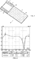
- Figure 1 shows two coplanar 2.4/5 GHz dual-band quarter-wave monopole antennas 1, 2 are closely spaced in a generally parallel arrangement on a PCB 3 comprising a dielectric substrate 4 with a conductive groundplane 5 over part of the substrate 4, and an area 6 free of groundplane 5 where the antennas 1, 2 are located.
- the width of the PCB 3 is 20 mm and the antenna area 6 clear of groundplane 5 is 15 mm long.
- the long lower portion 7 of the antenna is generally responsible for the radiation of 2.4 GHz and the elevated portions 1, 2 for the 5 GHz radiation.
- the height of the antenna at its tallest part is 3.2 mm.
- the monopole antennas 1, 2 are spaced only about ⁇ /6 apart and so the isolation between them is poor at around -6 dB, see Figure 2 .
- the monopole antennas 1, 2 are electrically further apart, but even so, the worst-case the isolation remains poor at around -8 dB.
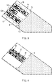
- Opt. A Pure Appl. Opt. 11 085101, 2009 ], but here one L-shape is inverted with respect to the other and not back-to-back as described in the present application. It has been found advantageous to use an unfilled array of elements 8, as shown in Figure 3 , where an element 8 is absent at location 12. Removing an element has been found to improve bandwidth and moving the remaining centre element 13 (in this example) up and down may be used to tune the bandwidth to a particular application.
- the metamaterial structure of Figure 3 provides good electromagnetic isolation at around 2.4 GHz.
- FIG. 4 An alternative metamaterial design is shown in Figure 4 , and is tuned to the 5 GHz band.
- a plurality of conductive LC elements 8' are printed on a single surface of FR4 substrate 9, but in the Figure 4 example, the elements 8' are conductively linked to each other and arranged as a pair of closely spaced columns. Other arrangments are possible.
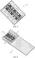
- a 5 GHz surface of the Figure 4 example can be mounted on top of and appropriately registered or aligned with a 2.4 GHz surface of the Figure 3 example, as shown in Figure 5 , to provide a dual-band metamaterial 14.
- Figure 6 shows a complete structure of a pair of monopole antennas 1, 2 on a PCB 3, with a dual-band combined metamaterial 14 of Figure 5 disposed between the monopole antennas 1, 2.
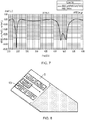
- the isolation between the antennas 1, 2 is improved in both bands, as shown in Figure 7 .
- the isolation In the lower 2.4 GHz band the isolation has a very deep null and even at the band edges it is around -12 dB. This could be improved by careful tuning of the metamaterial 14 to put the null exactly in the centre of the band.
- the isolation around 5 GHz In the high frequency band the isolation around 5 GHz is -20 dB. This notch may be moved to any part of the 4.9 - 5.9 GHz band by retuning the metamaterial 14.
- the lower layer of the dual-band metamaterial 14 is an unfilled array and has one element missing in the centre column (see Figure 3 ). Moving the position of the element within the column, see Figure 8 , can be used to change the bandwidth of isolation in the 5GHz band without much affecting the isolation frequency of the 2.4 GHz. This effect is shown in Figure 9 .
- the 2.4 GHz metamaterial has been shown as a 3x2 element array, whereas the 5 GHz metamaterial has been shown as a 2x3 array. It will be appreciated that other array configurations are possible with greater or smaller number of elements. It will also be appreciated that more than one array element may be removed to tune the bandwidth of the isolation effect.
- FR4 has been used as the substrate material.
- substrate material Many other types may be used including low and high dielectric materials.
- the beneficial characteristics of a metamaterial improve with increasing numbers of elements in the array.
- the use of a high dielectric substrate may be used to shrink the element size and allow more elements to be used in the array.
- n-band metamaterials can be created using n-layer substrates.
- isolation between two antennas has been described in the exemplary arrangement above, isolation between greater numbers is possible by suitably disposing metamaterial elements between all the pairs.
- the exemplary arrangement above describes two coplanar antennas, but the metamaterial described may also be used to improve isolation between antennas disposed using other geometries.
- Figure 10 shows a metamaterial comprising a 2D array of split-ring resonators 8 on a dielectric substrate 9 with one or more of the split-ring resonators 8 having a different size to the others. This may help to provide isolation over a wider bandwidth.
- Figure 11 shows a metamaterial comprising a 2D array of split-ring resonators 8 on a dielectric substrate 9 with one or more of the split-ring resonators 8 having a different shape to the others. This may help to provide isolation over a wider bandwidth.
- Figure 12 shows a metamaterial comprising a 2D array of split-ring resonators 8 having a first configuration on one surface of a dielectric substrate 9, and a 2D array of split-ring resonators 8' having a second, different configuration on the other surface of the dielectric substrate 9. This may help to provide isolation over a wider bandwidth.
- Figure 13 shows a metamaterial comprising a 2D array of split-ring resonators 8 having a first configuration on one surface of a dielectric substrate 9, a 2D array of split-ring resonators 8' having a second, different configuration on the other surface of the dielectric substrate 9, and an interstitial 2D array of split-ring resonators 8" having a third, different configuration between the surfaces of the dielectric substrate 9. This may help to provide isolation over a wider bandwidth.
Landscapes
- Details Of Aerials (AREA)
- Aerials With Secondary Devices (AREA)
- Variable-Direction Aerials And Aerial Arrays (AREA)
Applications Claiming Priority (2)
| Application Number | Priority Date | Filing Date | Title |
|---|---|---|---|
| GBGB1114625.5A GB201114625D0 (en) | 2011-08-24 | 2011-08-24 | Antenna isolation using metamaterial |
| PCT/GB2012/052010 WO2013027029A1 (en) | 2011-08-24 | 2012-08-16 | Antenna isolation using metamaterial |
Publications (2)
| Publication Number | Publication Date |
|---|---|
| EP2748893A1 EP2748893A1 (en) | 2014-07-02 |
| EP2748893B1 true EP2748893B1 (en) | 2019-09-25 |
Family
ID=44800820
Family Applications (1)
| Application Number | Title | Priority Date | Filing Date |
|---|---|---|---|
| EP12753577.1A Active EP2748893B1 (en) | 2011-08-24 | 2012-08-16 | Antenna isolation using metamaterial |
Country Status (7)
Families Citing this family (35)
| Publication number | Priority date | Publication date | Assignee | Title |
|---|---|---|---|---|
| US9837710B2 (en) | 2012-10-15 | 2017-12-05 | The Penn State Research Foundation | Broadband monopole antenna using anisotropic metamaterial coating |
| CN104466401B (zh) * | 2013-09-25 | 2019-03-12 | 中兴通讯股份有限公司 | 多天线终端 |
| CN104701624B (zh) * | 2015-03-03 | 2018-03-06 | 南京邮电大学 | 一种新型紧凑型的双频段mimo天线 |
| CN105006642A (zh) * | 2015-06-26 | 2015-10-28 | 桂林电子科技大学 | 单负材料隔离板及宽频高隔离度单极子阵列天线 |
| CN105006649A (zh) * | 2015-06-30 | 2015-10-28 | 厦门大学 | 一种电磁波近场隔离屏及其应用 |
| CN105006650B (zh) * | 2015-07-30 | 2018-03-09 | 中天宽带技术有限公司 | 一种基于光子晶体的双极化基站天线 |
| TWI608656B (zh) * | 2016-05-17 | 2017-12-11 | Slot antenna with complementary split ring | |
| CN106876982B (zh) * | 2017-02-22 | 2021-08-06 | 西安电子科技大学 | 改善多天线系统性能的超表面及采用超表面的多天线系统 |
| KR102008284B1 (ko) | 2017-03-29 | 2019-08-07 | 주식회사 케이원 | 식품소스 공급장치 |
| WO2018236202A1 (fr) * | 2017-04-28 | 2018-12-27 | Emsi Rabat | Dispositif de protection du corps humain et des équipements contre le rayonnement électromagnétique |
| GB201708242D0 (en) | 2017-05-23 | 2017-07-05 | Univ Bradford | Radiation shield |
| CN107069207A (zh) * | 2017-05-26 | 2017-08-18 | 南京信息工程大学 | 一种基于人工电磁超材料去耦的mimo天线 |
| CN107785661A (zh) * | 2017-10-18 | 2018-03-09 | 哈尔滨工程大学 | 一种基于双频超材料的去耦合阵列天线 |
| CN107968262B (zh) * | 2017-11-23 | 2021-03-19 | 广东通宇通讯股份有限公司 | 一种阵列天线及天线隔离组件 |
| KR101957798B1 (ko) * | 2018-01-17 | 2019-03-13 | 중앙대학교 산학협력단 | 메타물질 흡수체 |
| CN108511918B (zh) * | 2018-03-13 | 2020-08-28 | 东北石油大学 | 基于超材料的电磁波非对称传输控制器 |
| US10854986B2 (en) | 2018-07-18 | 2020-12-01 | Samsung Electro-Mechanics Co., Ltd. | Antenna apparatus |
| CN109638440B (zh) * | 2018-12-19 | 2020-05-12 | 电子科技大学 | 一种基于超材料的5g通信小型化宽频带mimo天线 |
| US12313570B2 (en) | 2019-03-27 | 2025-05-27 | Lyten, Inc. | Leaky coaxial resonant sensor systems and methods |
| US12317466B2 (en) | 2019-03-27 | 2025-05-27 | Lyten, Inc. | Frequency selective metamaterial for protective enclosures |
| US11965803B2 (en) * | 2019-03-27 | 2024-04-23 | Lyten, Inc. | Field deployable resonant sensors |
| US12270785B2 (en) | 2019-03-27 | 2025-04-08 | Lyten, Inc. | Water droplet sensing systems and methods |
| US12339272B2 (en) | 2019-03-27 | 2025-06-24 | Lyten, Inc. | Sensors incorporated into building materials to detect physical characteristic changes |
| US12196636B2 (en) | 2019-03-27 | 2025-01-14 | Lyten, Inc. | Sensors incorporated into airborne vehicle components to detect physical characteristic changes |
| US12265058B2 (en) | 2019-03-27 | 2025-04-01 | Lyten, Inc. | Sensors incorporated into adhesive material |
| KR102207150B1 (ko) | 2019-06-26 | 2021-01-25 | 삼성전기주식회사 | 안테나 장치 |
| CN112510366A (zh) * | 2020-10-19 | 2021-03-16 | 西安朗普达通信科技有限公司 | 一种级联式去耦芯片 |
| CN112382859A (zh) * | 2020-10-31 | 2021-02-19 | 华南理工大学 | 一种双电容太赫兹超材料电调控器件结构 |
| CN112968292B (zh) * | 2021-02-07 | 2022-09-16 | 北京邮电大学 | 可调太赫兹器件及可调天线 |
| CN113964490B (zh) * | 2021-09-17 | 2022-10-25 | 华南理工大学 | 一种宽带双极化电磁透明天线 |
| TWI800065B (zh) | 2021-10-29 | 2023-04-21 | 明泰科技股份有限公司 | 週期性金屬陣列結構 |
| US12103417B2 (en) | 2021-11-15 | 2024-10-01 | Toyota Motor Engineering & Manufacturing North America, Inc. | Metamaterial panel for enhancing wireless charging of electric vehicles |
| TWI838815B (zh) | 2022-08-08 | 2024-04-11 | 啟碁科技股份有限公司 | 天線模組、超材料結構及電子裝置 |
| US20240280526A1 (en) | 2023-02-15 | 2024-08-22 | Lyten, Inc. | Method of field recalibration of multivariate analyte sensors based on learned precise sensing fingerprints |
| WO2024241881A1 (ja) * | 2023-05-19 | 2024-11-28 | 京セラ株式会社 | 電波制御板 |
Family Cites Families (20)
| Publication number | Priority date | Publication date | Assignee | Title |
|---|---|---|---|---|
| JPH01149503A (ja) * | 1987-12-07 | 1989-06-12 | Nippon Telegr & Teleph Corp <Ntt> | リング型周波数選択板 |
| GB0130513D0 (en) * | 2001-12-20 | 2002-02-06 | Univ Southampton | Device for changing the polarization state of reflected transmitted and diffracted light and for achieving frequency and polarization sensitive reflection and |
| US6933895B2 (en) * | 2003-02-14 | 2005-08-23 | E-Tenna Corporation | Narrow reactive edge treatments and method for fabrication |
| US20050104678A1 (en) * | 2003-09-11 | 2005-05-19 | Shahrooz Shahparnia | System and method for noise mitigation in high speed printed circuit boards using electromagnetic bandgap structures |
| US7205941B2 (en) * | 2004-08-30 | 2007-04-17 | Hewlett-Packard Development Company, L.P. | Composite material with powered resonant cells |
| US7830310B1 (en) * | 2005-07-01 | 2010-11-09 | Hrl Laboratories, Llc | Artificial impedance structure |
| CN100372172C (zh) * | 2005-07-01 | 2008-02-27 | 清华大学 | 用于多输入多输出通信系统移动终端的平面四天线系统 |
| US7760140B2 (en) * | 2006-06-09 | 2010-07-20 | Intel Corporation | Multiband antenna array using electromagnetic bandgap structures |
| US7733289B2 (en) * | 2007-10-31 | 2010-06-08 | The Invention Science Fund I, Llc | Electromagnetic compression apparatus, methods, and systems |
| US7570432B1 (en) * | 2008-02-07 | 2009-08-04 | Toyota Motor Engineering & Manufacturing North America, Inc. | Metamaterial gradient index lens |
| US9116302B2 (en) * | 2008-06-19 | 2015-08-25 | Ravenbrick Llc | Optical metapolarizer device |
| JP5112204B2 (ja) * | 2008-07-15 | 2013-01-09 | 原田工業株式会社 | アンテナエレメント間の相互結合を抑制可能なアンテナ装置 |
| US7773033B2 (en) * | 2008-09-30 | 2010-08-10 | Raytheon Company | Multilayer metamaterial isolator |
| JP2010103609A (ja) * | 2008-10-21 | 2010-05-06 | Olympus Corp | 電磁波伝搬媒質 |
| CN201611683U (zh) * | 2008-11-20 | 2010-10-20 | 深圳大鹏光启科技有限公司 | 一种射频芯片小天线 |
| KR101262519B1 (ko) * | 2009-01-21 | 2013-05-08 | 라벤브릭 엘엘씨 | 광학 메타편광자 장치 |
| KR101202339B1 (ko) * | 2009-04-29 | 2012-11-16 | 한국전자통신연구원 | 메타물질 상판덮개를 이용한 이득향상과 빔 성형이 동시에 가능한 안테나 |
| TWI420739B (zh) * | 2009-05-21 | 2013-12-21 | Ind Tech Res Inst | 輻射場型隔離器及其天線系統與使用該天線系統的通訊裝置 |
| WO2012126249A1 (zh) * | 2011-03-18 | 2012-09-27 | 深圳光启高等理工研究院 | 一种实现电磁波偏折的超材料 |
| EP2518824A1 (en) * | 2011-04-27 | 2012-10-31 | Research In Motion Limited | Multiple antenna assembly utilizing electromagnetic band gap isolation structures |
-
2011
- 2011-08-24 GB GBGB1114625.5A patent/GB201114625D0/en not_active Ceased
-
2012
- 2012-08-16 GB GB1214655.1A patent/GB2495365A/en not_active Withdrawn
- 2012-08-16 CN CN201280052230.1A patent/CN103999286B/zh active Active
- 2012-08-16 WO PCT/GB2012/052010 patent/WO2013027029A1/en active Application Filing
- 2012-08-16 KR KR1020147004604A patent/KR101944568B1/ko active Active
- 2012-08-16 JP JP2014526550A patent/JP2014527366A/ja active Pending
- 2012-08-16 EP EP12753577.1A patent/EP2748893B1/en active Active
- 2012-08-22 TW TW101130347A patent/TWI590523B/zh not_active IP Right Cessation
Non-Patent Citations (1)
| Title |
|---|
| None * |
Also Published As
| Publication number | Publication date |
|---|---|
| TW201320467A (zh) | 2013-05-16 |
| KR20140050684A (ko) | 2014-04-29 |
| CN103999286B (zh) | 2016-10-26 |
| KR101944568B1 (ko) | 2019-01-31 |
| CN103999286A (zh) | 2014-08-20 |
| GB201114625D0 (en) | 2011-10-05 |
| JP2014527366A (ja) | 2014-10-09 |
| TWI590523B (zh) | 2017-07-01 |
| GB201214655D0 (en) | 2012-10-03 |
| WO2013027029A1 (en) | 2013-02-28 |
| GB2495365A (en) | 2013-04-10 |
| EP2748893A1 (en) | 2014-07-02 |
Similar Documents
| Publication | Publication Date | Title |
|---|---|---|
| EP2748893B1 (en) | Antenna isolation using metamaterial | |
| EP3320580B1 (en) | Metamaterial-based transmitarray for multi-beam antenna array assemblies | |
| Alam et al. | Development of electromagnetic band gap structures in the perspective of microstrip antenna design | |
| Li et al. | Miniaturized double-layer EBG structures for broadband mutual coupling reduction between UWB monopoles | |
| Gong et al. | Multi-band and high gain antenna using AMC ground characterized with four zero-phases of reflection coefficient | |
| US10446923B2 (en) | Antenna array with reduced mutual coupling effect | |
| US20130147673A1 (en) | Metamaterial loaded antenna structures | |
| Sokunbi et al. | Highly reduced mutual coupling between wideband patch antenna array using multiresonance EBG structure and defective ground surface | |
| Borazjani et al. | Bandwidth improvement of planar antennas using a single-layer metamaterial substrate for X-band application | |
| Saad et al. | Wideband slotted planar antenna with defected ground structure | |
| KR101014972B1 (ko) | 메타머티리얼 안테나 및 이를 이용한 통신 장치 | |
| Li et al. | A high selectivity, miniaturized, low profile dual‐band bandpass FSS with a controllable transmission zero | |
| Manage et al. | A Survey on applications of Metamaterials in Antenna Design | |
| Joshi et al. | Rectangular slotted microstrip patch antenna with partially loaded metamaterial ground plane | |
| Parmar et al. | A Comprehensive Survey of Microstrip Patch Antenna based on Metamaterial | |
| Foo | Metamaterial-based transmitarray for orthogonal-beam-space massive-MIMO | |
| Nguyen et al. | Design of compact EBG structure for array antenna application | |
| Aziz et al. | Electromagnetic effect of rectangular spiral metamaterial on microstrip patch antenna performance | |
| Prakash et al. | Multilayer Complementary Frequency Selective Surfaces with Hybrid Functionality | |
| Kamiya et al. | Study of EBG structures using Metamaterial Technology | |
| Chu et al. | High efficiency small antenna for WLAN application | |
| KR20150017872A (ko) | 튜너블 캐패시턴스를 이용한 mtm 안테나 | |
| Sittakul et al. | Compact multiband L-shaped slot antenna using complementary split ring resonator for WLAN applications | |
| Gnanasundar | Study of Electromagnetic Band Gap Structures for Antenna Application | |
| ISMAIL et al. | RECONFIGURABLE COMPOSITE RIGHT/LEFT-HANDED TRANSMISSION LINE ANTENNA BASED MINKOWSKI-STEPPED IMPEDANCE RESONATOR STRUCTURE FOR 5G COMMUNICATION NETWORKS |
Legal Events
| Date | Code | Title | Description |
|---|---|---|---|
| PUAI | Public reference made under article 153(3) epc to a published international application that has entered the european phase |
Free format text: ORIGINAL CODE: 0009012 |
|
| 17P | Request for examination filed |
Effective date: 20140220 |
|
| AK | Designated contracting states |
Kind code of ref document: A1 Designated state(s): AL AT BE BG CH CY CZ DE DK EE ES FI FR GB GR HR HU IE IS IT LI LT LU LV MC MK MT NL NO PL PT RO RS SE SI SK SM TR |
|
| DAX | Request for extension of the european patent (deleted) | ||
| RAP1 | Party data changed (applicant data changed or rights of an application transferred) |
Owner name: MICROSOFT TECHNOLOGY LICENSING, LLC |
|
| STAA | Information on the status of an ep patent application or granted ep patent |
Free format text: STATUS: EXAMINATION IS IN PROGRESS |
|
| 17Q | First examination report despatched |
Effective date: 20170822 |
|
| GRAP | Despatch of communication of intention to grant a patent |
Free format text: ORIGINAL CODE: EPIDOSNIGR1 |
|
| STAA | Information on the status of an ep patent application or granted ep patent |
Free format text: STATUS: GRANT OF PATENT IS INTENDED |
|
| INTG | Intention to grant announced |
Effective date: 20190418 |
|
| GRAS | Grant fee paid |
Free format text: ORIGINAL CODE: EPIDOSNIGR3 |
|
| GRAA | (expected) grant |
Free format text: ORIGINAL CODE: 0009210 |
|
| STAA | Information on the status of an ep patent application or granted ep patent |
Free format text: STATUS: THE PATENT HAS BEEN GRANTED |
|
| AK | Designated contracting states |
Kind code of ref document: B1 Designated state(s): AL AT BE BG CH CY CZ DE DK EE ES FI FR GB GR HR HU IE IS IT LI LT LU LV MC MK MT NL NO PL PT RO RS SE SI SK SM TR |
|
| REG | Reference to a national code |
Ref country code: GB Ref legal event code: FG4D |
|
| REG | Reference to a national code |
Ref country code: CH Ref legal event code: EP |
|
| REG | Reference to a national code |
Ref country code: AT Ref legal event code: REF Ref document number: 1184735 Country of ref document: AT Kind code of ref document: T Effective date: 20191015 |
|
| REG | Reference to a national code |
Ref country code: IE Ref legal event code: FG4D |
|
| REG | Reference to a national code |
Ref country code: DE Ref legal event code: R096 Ref document number: 602012064329 Country of ref document: DE |
|
| REG | Reference to a national code |
Ref country code: NL Ref legal event code: FP |
|
| PG25 | Lapsed in a contracting state [announced via postgrant information from national office to epo] |
Ref country code: BG Free format text: LAPSE BECAUSE OF FAILURE TO SUBMIT A TRANSLATION OF THE DESCRIPTION OR TO PAY THE FEE WITHIN THE PRESCRIBED TIME-LIMIT Effective date: 20191225 Ref country code: NO Free format text: LAPSE BECAUSE OF FAILURE TO SUBMIT A TRANSLATION OF THE DESCRIPTION OR TO PAY THE FEE WITHIN THE PRESCRIBED TIME-LIMIT Effective date: 20191225 Ref country code: FI Free format text: LAPSE BECAUSE OF FAILURE TO SUBMIT A TRANSLATION OF THE DESCRIPTION OR TO PAY THE FEE WITHIN THE PRESCRIBED TIME-LIMIT Effective date: 20190925 Ref country code: LT Free format text: LAPSE BECAUSE OF FAILURE TO SUBMIT A TRANSLATION OF THE DESCRIPTION OR TO PAY THE FEE WITHIN THE PRESCRIBED TIME-LIMIT Effective date: 20190925 Ref country code: SE Free format text: LAPSE BECAUSE OF FAILURE TO SUBMIT A TRANSLATION OF THE DESCRIPTION OR TO PAY THE FEE WITHIN THE PRESCRIBED TIME-LIMIT Effective date: 20190925 Ref country code: HR Free format text: LAPSE BECAUSE OF FAILURE TO SUBMIT A TRANSLATION OF THE DESCRIPTION OR TO PAY THE FEE WITHIN THE PRESCRIBED TIME-LIMIT Effective date: 20190925 |
|
| REG | Reference to a national code |
Ref country code: LT Ref legal event code: MG4D |
|
| PG25 | Lapsed in a contracting state [announced via postgrant information from national office to epo] |
Ref country code: GR Free format text: LAPSE BECAUSE OF FAILURE TO SUBMIT A TRANSLATION OF THE DESCRIPTION OR TO PAY THE FEE WITHIN THE PRESCRIBED TIME-LIMIT Effective date: 20191226 Ref country code: RS Free format text: LAPSE BECAUSE OF FAILURE TO SUBMIT A TRANSLATION OF THE DESCRIPTION OR TO PAY THE FEE WITHIN THE PRESCRIBED TIME-LIMIT Effective date: 20190925 Ref country code: LV Free format text: LAPSE BECAUSE OF FAILURE TO SUBMIT A TRANSLATION OF THE DESCRIPTION OR TO PAY THE FEE WITHIN THE PRESCRIBED TIME-LIMIT Effective date: 20190925 |
|
| REG | Reference to a national code |
Ref country code: AT Ref legal event code: MK05 Ref document number: 1184735 Country of ref document: AT Kind code of ref document: T Effective date: 20190925 |
|
| PG25 | Lapsed in a contracting state [announced via postgrant information from national office to epo] |
Ref country code: IT Free format text: LAPSE BECAUSE OF FAILURE TO SUBMIT A TRANSLATION OF THE DESCRIPTION OR TO PAY THE FEE WITHIN THE PRESCRIBED TIME-LIMIT Effective date: 20190925 Ref country code: AL Free format text: LAPSE BECAUSE OF FAILURE TO SUBMIT A TRANSLATION OF THE DESCRIPTION OR TO PAY THE FEE WITHIN THE PRESCRIBED TIME-LIMIT Effective date: 20190925 Ref country code: EE Free format text: LAPSE BECAUSE OF FAILURE TO SUBMIT A TRANSLATION OF THE DESCRIPTION OR TO PAY THE FEE WITHIN THE PRESCRIBED TIME-LIMIT Effective date: 20190925 Ref country code: PL Free format text: LAPSE BECAUSE OF FAILURE TO SUBMIT A TRANSLATION OF THE DESCRIPTION OR TO PAY THE FEE WITHIN THE PRESCRIBED TIME-LIMIT Effective date: 20190925 Ref country code: AT Free format text: LAPSE BECAUSE OF FAILURE TO SUBMIT A TRANSLATION OF THE DESCRIPTION OR TO PAY THE FEE WITHIN THE PRESCRIBED TIME-LIMIT Effective date: 20190925 Ref country code: ES Free format text: LAPSE BECAUSE OF FAILURE TO SUBMIT A TRANSLATION OF THE DESCRIPTION OR TO PAY THE FEE WITHIN THE PRESCRIBED TIME-LIMIT Effective date: 20190925 Ref country code: PT Free format text: LAPSE BECAUSE OF FAILURE TO SUBMIT A TRANSLATION OF THE DESCRIPTION OR TO PAY THE FEE WITHIN THE PRESCRIBED TIME-LIMIT Effective date: 20200127 Ref country code: RO Free format text: LAPSE BECAUSE OF FAILURE TO SUBMIT A TRANSLATION OF THE DESCRIPTION OR TO PAY THE FEE WITHIN THE PRESCRIBED TIME-LIMIT Effective date: 20190925 |
|
| PG25 | Lapsed in a contracting state [announced via postgrant information from national office to epo] |
Ref country code: IS Free format text: LAPSE BECAUSE OF FAILURE TO SUBMIT A TRANSLATION OF THE DESCRIPTION OR TO PAY THE FEE WITHIN THE PRESCRIBED TIME-LIMIT Effective date: 20200224 Ref country code: CZ Free format text: LAPSE BECAUSE OF FAILURE TO SUBMIT A TRANSLATION OF THE DESCRIPTION OR TO PAY THE FEE WITHIN THE PRESCRIBED TIME-LIMIT Effective date: 20190925 Ref country code: SM Free format text: LAPSE BECAUSE OF FAILURE TO SUBMIT A TRANSLATION OF THE DESCRIPTION OR TO PAY THE FEE WITHIN THE PRESCRIBED TIME-LIMIT Effective date: 20190925 Ref country code: SK Free format text: LAPSE BECAUSE OF FAILURE TO SUBMIT A TRANSLATION OF THE DESCRIPTION OR TO PAY THE FEE WITHIN THE PRESCRIBED TIME-LIMIT Effective date: 20190925 |
|
| REG | Reference to a national code |
Ref country code: DE Ref legal event code: R097 Ref document number: 602012064329 Country of ref document: DE |
|
| PG2D | Information on lapse in contracting state deleted |
Ref country code: IS |
|
| PG25 | Lapsed in a contracting state [announced via postgrant information from national office to epo] |
Ref country code: DK Free format text: LAPSE BECAUSE OF FAILURE TO SUBMIT A TRANSLATION OF THE DESCRIPTION OR TO PAY THE FEE WITHIN THE PRESCRIBED TIME-LIMIT Effective date: 20190925 Ref country code: IS Free format text: LAPSE BECAUSE OF FAILURE TO SUBMIT A TRANSLATION OF THE DESCRIPTION OR TO PAY THE FEE WITHIN THE PRESCRIBED TIME-LIMIT Effective date: 20200126 |
|
| PLBE | No opposition filed within time limit |
Free format text: ORIGINAL CODE: 0009261 |
|
| STAA | Information on the status of an ep patent application or granted ep patent |
Free format text: STATUS: NO OPPOSITION FILED WITHIN TIME LIMIT |
|
| 26N | No opposition filed |
Effective date: 20200626 |
|
| PG25 | Lapsed in a contracting state [announced via postgrant information from national office to epo] |
Ref country code: SI Free format text: LAPSE BECAUSE OF FAILURE TO SUBMIT A TRANSLATION OF THE DESCRIPTION OR TO PAY THE FEE WITHIN THE PRESCRIBED TIME-LIMIT Effective date: 20190925 |
|
| PG25 | Lapsed in a contracting state [announced via postgrant information from national office to epo] |
Ref country code: MC Free format text: LAPSE BECAUSE OF FAILURE TO SUBMIT A TRANSLATION OF THE DESCRIPTION OR TO PAY THE FEE WITHIN THE PRESCRIBED TIME-LIMIT Effective date: 20190925 |
|
| REG | Reference to a national code |
Ref country code: CH Ref legal event code: PL |
|
| PG25 | Lapsed in a contracting state [announced via postgrant information from national office to epo] |
Ref country code: CH Free format text: LAPSE BECAUSE OF NON-PAYMENT OF DUE FEES Effective date: 20200831 Ref country code: LI Free format text: LAPSE BECAUSE OF NON-PAYMENT OF DUE FEES Effective date: 20200831 Ref country code: LU Free format text: LAPSE BECAUSE OF NON-PAYMENT OF DUE FEES Effective date: 20200816 |
|
| REG | Reference to a national code |
Ref country code: BE Ref legal event code: MM Effective date: 20200831 |
|
| PG25 | Lapsed in a contracting state [announced via postgrant information from national office to epo] |
Ref country code: BE Free format text: LAPSE BECAUSE OF NON-PAYMENT OF DUE FEES Effective date: 20200831 Ref country code: IE Free format text: LAPSE BECAUSE OF NON-PAYMENT OF DUE FEES Effective date: 20200816 |
|
| PG25 | Lapsed in a contracting state [announced via postgrant information from national office to epo] |
Ref country code: TR Free format text: LAPSE BECAUSE OF FAILURE TO SUBMIT A TRANSLATION OF THE DESCRIPTION OR TO PAY THE FEE WITHIN THE PRESCRIBED TIME-LIMIT Effective date: 20190925 Ref country code: MT Free format text: LAPSE BECAUSE OF FAILURE TO SUBMIT A TRANSLATION OF THE DESCRIPTION OR TO PAY THE FEE WITHIN THE PRESCRIBED TIME-LIMIT Effective date: 20190925 Ref country code: CY Free format text: LAPSE BECAUSE OF FAILURE TO SUBMIT A TRANSLATION OF THE DESCRIPTION OR TO PAY THE FEE WITHIN THE PRESCRIBED TIME-LIMIT Effective date: 20190925 |
|
| PG25 | Lapsed in a contracting state [announced via postgrant information from national office to epo] |
Ref country code: MK Free format text: LAPSE BECAUSE OF FAILURE TO SUBMIT A TRANSLATION OF THE DESCRIPTION OR TO PAY THE FEE WITHIN THE PRESCRIBED TIME-LIMIT Effective date: 20190925 |
|
| P01 | Opt-out of the competence of the unified patent court (upc) registered |
Effective date: 20230501 |
|
| PGFP | Annual fee paid to national office [announced via postgrant information from national office to epo] |
Ref country code: NL Payment date: 20230721 Year of fee payment: 12 |
|
| PGFP | Annual fee paid to national office [announced via postgrant information from national office to epo] |
Ref country code: GB Payment date: 20230720 Year of fee payment: 12 |
|
| PGFP | Annual fee paid to national office [announced via postgrant information from national office to epo] |
Ref country code: FR Payment date: 20230720 Year of fee payment: 12 |
|
| PGFP | Annual fee paid to national office [announced via postgrant information from national office to epo] |
Ref country code: DE Payment date: 20240723 Year of fee payment: 13 |
|
| REG | Reference to a national code |
Ref country code: NL Ref legal event code: MM Effective date: 20240901 |
|
| GBPC | Gb: european patent ceased through non-payment of renewal fee |
Effective date: 20240816 |
|
| PG25 | Lapsed in a contracting state [announced via postgrant information from national office to epo] |
Ref country code: NL Free format text: LAPSE BECAUSE OF NON-PAYMENT OF DUE FEES Effective date: 20240901 |
|
| PG25 | Lapsed in a contracting state [announced via postgrant information from national office to epo] |
Ref country code: GB Free format text: LAPSE BECAUSE OF NON-PAYMENT OF DUE FEES Effective date: 20240816 |
|
| PG25 | Lapsed in a contracting state [announced via postgrant information from national office to epo] |
Ref country code: FR Free format text: LAPSE BECAUSE OF NON-PAYMENT OF DUE FEES Effective date: 20240831 |