EP2747231A1 - Hardware-based, redundant overvoltage protection - Google Patents
Hardware-based, redundant overvoltage protection Download PDFInfo
- Publication number
- EP2747231A1 EP2747231A1 EP13196266.4A EP13196266A EP2747231A1 EP 2747231 A1 EP2747231 A1 EP 2747231A1 EP 13196266 A EP13196266 A EP 13196266A EP 2747231 A1 EP2747231 A1 EP 2747231A1
- Authority
- EP
- European Patent Office
- Prior art keywords
- overvoltage
- generator
- fault signal
- gcu
- detection circuit
- Prior art date
- Legal status (The legal status is an assumption and is not a legal conclusion. Google has not performed a legal analysis and makes no representation as to the accuracy of the status listed.)
- Granted
Links
- 238000001514 detection method Methods 0.000 claims abstract description 58
- 230000005284 excitation Effects 0.000 claims description 22
- 238000004804 winding Methods 0.000 claims description 21
- 230000033228 biological regulation Effects 0.000 claims description 12
- 238000001914 filtration Methods 0.000 claims description 5
- 230000003750 conditioning effect Effects 0.000 description 11
- 238000010586 diagram Methods 0.000 description 6
- 238000012545 processing Methods 0.000 description 5
- 238000004891 communication Methods 0.000 description 2
- 230000001143 conditioned effect Effects 0.000 description 2
- 238000002955 isolation Methods 0.000 description 2
- 230000007935 neutral effect Effects 0.000 description 2
- 238000012360 testing method Methods 0.000 description 2
- 230000001276 controlling effect Effects 0.000 description 1
- 230000007423 decrease Effects 0.000 description 1
- 230000005669 field effect Effects 0.000 description 1
- 239000000463 material Substances 0.000 description 1
- 229910044991 metal oxide Inorganic materials 0.000 description 1
- 150000004706 metal oxides Chemical class 0.000 description 1
- 238000012986 modification Methods 0.000 description 1
- 230000004048 modification Effects 0.000 description 1
- 238000012544 monitoring process Methods 0.000 description 1
- 230000001681 protective effect Effects 0.000 description 1
- 230000001105 regulatory effect Effects 0.000 description 1
- 239000004065 semiconductor Substances 0.000 description 1
- 230000001960 triggered effect Effects 0.000 description 1
Images

Classifications
-
- H—ELECTRICITY
- H02—GENERATION; CONVERSION OR DISTRIBUTION OF ELECTRIC POWER
- H02H—EMERGENCY PROTECTIVE CIRCUIT ARRANGEMENTS
- H02H7/00—Emergency protective circuit arrangements specially adapted for specific types of electric machines or apparatus or for sectionalised protection of cable or line systems, and effecting automatic switching in the event of an undesired change from normal working conditions
- H02H7/06—Emergency protective circuit arrangements specially adapted for specific types of electric machines or apparatus or for sectionalised protection of cable or line systems, and effecting automatic switching in the event of an undesired change from normal working conditions for dynamo-electric generators; for synchronous capacitors
-
- H—ELECTRICITY
- H02—GENERATION; CONVERSION OR DISTRIBUTION OF ELECTRIC POWER
- H02H—EMERGENCY PROTECTIVE CIRCUIT ARRANGEMENTS
- H02H3/00—Emergency protective circuit arrangements for automatic disconnection directly responsive to an undesired change from normal electric working condition with or without subsequent reconnection ; integrated protection
- H02H3/02—Details
- H02H3/05—Details with means for increasing reliability, e.g. redundancy arrangements
-
- H—ELECTRICITY
- H02—GENERATION; CONVERSION OR DISTRIBUTION OF ELECTRIC POWER
- H02H—EMERGENCY PROTECTIVE CIRCUIT ARRANGEMENTS
- H02H7/00—Emergency protective circuit arrangements specially adapted for specific types of electric machines or apparatus or for sectionalised protection of cable or line systems, and effecting automatic switching in the event of an undesired change from normal working conditions
- H02H7/06—Emergency protective circuit arrangements specially adapted for specific types of electric machines or apparatus or for sectionalised protection of cable or line systems, and effecting automatic switching in the event of an undesired change from normal working conditions for dynamo-electric generators; for synchronous capacitors
- H02H7/065—Emergency protective circuit arrangements specially adapted for specific types of electric machines or apparatus or for sectionalised protection of cable or line systems, and effecting automatic switching in the event of an undesired change from normal working conditions for dynamo-electric generators; for synchronous capacitors against excitation faults
-
- H—ELECTRICITY
- H02—GENERATION; CONVERSION OR DISTRIBUTION OF ELECTRIC POWER
- H02P—CONTROL OR REGULATION OF ELECTRIC MOTORS, ELECTRIC GENERATORS OR DYNAMO-ELECTRIC CONVERTERS; CONTROLLING TRANSFORMERS, REACTORS OR CHOKE COILS
- H02P9/00—Arrangements for controlling electric generators for the purpose of obtaining a desired output
- H02P9/006—Means for protecting the generator by using control
-
- H—ELECTRICITY
- H02—GENERATION; CONVERSION OR DISTRIBUTION OF ELECTRIC POWER
- H02P—CONTROL OR REGULATION OF ELECTRIC MOTORS, ELECTRIC GENERATORS OR DYNAMO-ELECTRIC CONVERTERS; CONTROLLING TRANSFORMERS, REACTORS OR CHOKE COILS
- H02P9/00—Arrangements for controlling electric generators for the purpose of obtaining a desired output
- H02P9/10—Control effected upon generator excitation circuit to reduce harmful effects of overloads or transients, e.g. sudden application of load, sudden removal of load, sudden change of load
- H02P9/102—Control effected upon generator excitation circuit to reduce harmful effects of overloads or transients, e.g. sudden application of load, sudden removal of load, sudden change of load for limiting effects of transients
Definitions
- the present invention is related to generator controllers, and in particular to overvoltage protection provided by generator controllers.
- GCUs Generator controllers, commonly referred to as generator control units (GCUs), regulate the operation of associated generators. For example, in a generator excited by an exciter winding, the GCU monitors the output voltage of the generator and executes software to regulate the output voltage to a desired value. In addition, the GCU executes software to compare the monitored output voltage to a threshold to determine whether an overvoltage fault condition exists that requires the generator to be shut down. This may include removing excitation from the generator exciter drive, opening contactors connecting the generator output to a distribution system, or other actions.
- GCUs generator control units
- a generator system includes a generator and a generator control unit (GCU).
- the GCU is connected to monitor and regulate the generator output voltage.
- the GCU includes a protection signal processor that receives monitored generator voltages and executes software to detect an overvoltage condition.
- the GCU further includes redundant, hardware based overvoltage detection that detects a peak voltage value associated with the monitored generator voltage and includes a fast overvoltage detection circuit that generates a first overvoltage fault signal if the peak voltage value is greater than a first threshold value and includes an inverse overvoltage detection circuit that generates a second overvoltage fault signal if the peak voltage value is greater than a second threshold value for a duration of time that varies with a magnitude of the peak voltage value.
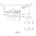
- Fig. 1 is a block diagram of a generator system 10 according to an embodiment of the present invention.
- Generator system 10 includes variable frequency generator (VFG) 12, generator control unit (GCU) 14, alternating current (AC) bus 16 and one or more loads 18.
- Generator control unit (GCU) 14 includes rectifier 20, generator control relay 22, exciter drive 24, and control/protection circuit 26.
- generator 12 is a variable frequency wound-field generator, in which the main output of the generator is a function of the current (labeled 'exciter field control') supplied to the exciter field winding (not shown), although in other embodiment VFG 12 may be implemented with other well-known generator types. Throughout this application, VFG 12 is referred to simply as generator 12.
- generator 12 includes a permanent magnet generator portion (not shown) that generates an alternating current (AC) voltage labeled PMG_V that is provided to GCU 14 and used to selectively excite the exciter field winding.
- the main output of generator 12 is provided via AC bus 16 to one or more of a plurality of loads 18.
- other types of well-known generator topologies may be employed to excite the wound-field generator and regulate the output of said generator.
- lines indicative of power being transferred are shown in thicker outline, while lines representative of monitored signals or communication signals are shown in thinner outline.
- GCU 14 regulates the output of generator 12.
- GCU 14 monitors the main output POR_V of generator 12 at a point of regulation (POR), and selectively controls the excitation (exciter field control) provided to the exciter field winding of generator 12.
- Excitation for the exciter winding is provided by the AC voltage PMG_V provided by the permanent magnet generator portion of generator 12.
- the PMG voltage is illustrated with a thicker line to indicate that power is being supplied to GCU 14 from the permanent magnet generator portion.
- Rectifier 20 rectifies the AC voltage PMG_V and provides a rectified or DC voltage via GCR 22 to exciter drive 24.
- Control and protection circuit 26 which receives inputs regarding the monitored output voltage POR_V at the point of regulation of generator 12, selectively controls the operation of exciter drive 24 in exciting the field winding.
- exciter drive 24 may consist of one or more solid-state switches selectively turned On and Off by control/protection circuit 26 to provide the DC output provided by rectifier 20 to the exciter field winding of generator 12.
- one embodiment may employ a single solid-state switch for controlling the application of power to the exciter field winding while other embodiments may make use of both a high-side and low-side switch for selectively applying power to the exciter field winding.
- GCU 14 provides overvoltage protection of generator 12.
- control and protection circuit 26 monitors at the output voltage POR_V of generator 12 and in response to the monitored voltage exceeding a threshold voltage acts to protect generator 12. This may include commanding exciter drive 24 to remove excitation provided to generator 12, opening generator control relay (GCR) 22 to remove excitation from being provided to exciter drive 24, and/or opening generator line contactor (GLC) 28 to disconnect generator 12 from AC bus 16.
- GCR generator control relay
- GLC generator line contactor
- control and protection circuit 26 provides software-implemented overvoltage protection as well as both fast and slow overvoltage protection implemented in hardware that is redundant to the protection provided in software.
- GCU 14 may monitor output current Line_CT associated with generator 12 via current sensor 29.
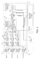
- Fig. 2 is a block diagram of a generator controller unit 14 that illustrates the combination of software and hardware overvoltage protection implemented according to an embodiment of the present invention.
- GCU 14 monitors the generator output voltage POR_V and through various signal processing steps acts to regulate the generator output voltage by selectively regulating the excitation provided to generator 12 via exciter drive 24 (as shown in Fig. 1 ).
- GCU 14 provides overvoltage protection in response to the monitored generator output voltage POR_V.
- GCU 14 includes a plurality of different modules, including system module 30, signal processing module 32, exciter drive module 34, backplane module 36, and interconnection module 38.
- Exciter drive module 34 includes an input for receiving via backplane module 36 the AC voltage generated by the permanent magnet generator (PMG).
- Exciter drive module 34 includes rectifier 20, generator control relay (GCR) 22, and exciter drive 24, each of which are shown in FIG. 1 , as well as exciter control 40.
- Rectifier 20 rectifies the AC voltage received from PMG armature winding of generator 12 (shown in FIG. 1 ) to a DC voltage.
- Exciter drive 24 is selectively turned On and Off based on commands received from exciter control 40 to regulate the current supplied to the exciter winding.
- a solid-state switch such as a metal-oxide semiconductor field-effect transistor (MOSFET) may be employed by exciter drive 24 to selectively control the application of power to an exciter field winding of generator 12.
- GCR 22 is a protective relay used to disconnect power from being supplied to the exciter field winding in the event of an overvoltage condition. In this way, GCR 22 provides overvoltage protection in the event exciter drive 24 fails (e.g., fails closed, preventing regulation of current supplied to the exciter field winding).
- GCR 22 is located in series on the negative or return path of the DC voltage provided to exciter drive 24, but in other embodiments could be connected on the positive path.
- System module 30 and signal processing module 32 together provide much of the functionality described with respect to control/protection circuit 26 (shown in FIG. 1 ).
- signal processing module 32 receives as inputs the monitored generator current (Gen_CT) and the monitored generator output voltage (PORV) monitored at the point of regulation.
- the monitored generator current and voltage are conditioned by signal condition circuits 42 and 44, each providing redundant signal conditioning of both the monitored current and voltage.
- the output of signal conditioning circuit 42 is provided to voltage regulation (VR) signal processor 46, while the output of signal conditioning circuit 44 is provided to protection signal processor 48.
- VR voltage regulation
- protection signal processor 48 In the embodiment shown in Fig. 2 , both VR signal processor 46 and protection signal processor 48 are implemented with digital signal processors (DSPs).
- VR signal processor 46 In response to the monitored generator current and voltage, VR signal processor 46 generates an exciter command signal Exciter_Cmd that is provided to exciter drive modulator 50. Based on the received exciter command signal, exciter drive modulator 50 generates a pulse width modulated signal (PWM) that is provided to exciter control 30, which generates the drive signal supplied to exciter drive 24.
- PWM pulse width modulated signal
- VR signal processor 46 communicates with system control and protection processor 54 regarding the status of the monitored generator outputs and exciter commands. In the embodiment shown in Fig. 2 , VR signal processor 46 communicates with system control and protection processor 54 via a controller area network (CAN) bus, although in other embodiments various communication buses and protocols may be employed.
- CAN controller area network
- signal processing module 62 also provides redundant overvoltage protection.
- the monitored generator current Gen_CT and the monitored generator output voltage are provided to signal conditioning circuit 44.
- the conditioned outputs are provided to protection signal processor 48.
- protection signal processor 48 Based on the monitored generator current and generator output voltage, protection signal processor 48 detects, among other fault conditions, overvoltage conditions. Detected fault conditions such as overvoltage faults are communicated to system control and protection processor 54.
- system control and protection processor 54 In response to a detected overvoltage condition, system control and protection processor 54 provides a fault signal that is communicated to exciter drive modulation circuit 50 to turn Off or remove the excitation provided to generator 12.
- system control and protection processor 54 receives feedback from exciter drive fast protection interface circuit 52, which detects fault conditions in exciter drive circuit 24. In response to a fault condition in exciter drive circuit 24, system control and protection processor 54 generates a fault condition that is provided to exciter drive modulation circuit 50 to remove the excitation provided to generator 12.
- protection signal processor 48 is a digital signal processor that executes software to detect an overvoltage fault condition.
- system control and protection processor 54 is a processor that executes software to respond to inputs provided by protection signal processor 48 and exciter drive fast protection interface 52 to remove excitation provided to generator 12.
- GCU 14 includes redundant, hardware-based overvoltage protection circuit 58 that includes highest peak detect circuit 60, redundant overvoltage (ROV) detection circuit 62, ROV latch circuit 64, and ROV built-in test circuit 66.
- ROV redundant overvoltage
- Monitored phase voltages provided to signal conditioning circuit 44 are provided to highest peak detect circuit 60, which identifies a highest peak voltage value from the monitored phase voltages and provides the peak voltage value Vin to ROV detection circuit 62.
- ROV detection circuit 62 compares the peak voltage value Vin to a reference value Vref. If the peak voltage value Vin is greater than the reference value Vref, then ROV detection circuit 62 generates a fault signal ROV_fault.
- ROV latch circuit 64 latches the fault signal and provides the latched output indicating a fault to fault-OR circuit 56. ROV latch circuit 64 remains latched until a reset signal is received from system control and protection circuit 54.
- the ROV fault signal provided by ROV latch circuit 64 is combined via a logical OR operation with the fast fault signal provided by system control and protection processor 54. That is, if either the ROV fault signal or the fast fault signal indicate a fault condition, then the output of fault-OR circuit 56 provided to exciter drive modulation circuit 50 indicates a fault condition. In response to an indicated fault condition, exciter drive modulation circuit 50 provides a signal to exciter control circuit 40 with instructions to remove excitation from generator 12. With respect to faults generated by hardware redundant OV protection circuit 58, the fault condition persists until system control and protection processor 54 resets ROV latch 64, thereby clearing the fault. System control and protection processor 54 monitors the ROV fault signal provided by ROV latch circuit 64.
- system control and protection processor 54 provides a ROV stim signal to ROV BIT circuit 66 to initiate a built-in test of ROV detection circuit 62. That is, a fault is injected into ROV detection circuit 62, and system control and protection processor 54 monitors the ROV fault signal provided by ROV latch circuit 64 to ensure the fault is handled properly.
- the present invention provides in hardware, overvoltage protection that is redundant to overvoltage protection provided by protection signal processor 48, and as such is not susceptible to software faults.
- hardware overvoltage protection circuit 58 is described throughout as providing redundant fault detection (albeit, implemented in hardware), it should be understood that the thresholds employed by hardware-based overvoltage protection circuit 58 may differ from the thresholds employed by protection signal processor 48. That is, protection signal processor 48 may implement fault detection at a first threshold value, while hardware overvoltage protection circuit 58 implements fault detection at a second threshold value.
- hardware overvoltage protection circuit 58 may also implement "fast” and “slow” overvoltage protection.
- Fast overvoltage protection is implemented by comparing the peak voltage Vin to a reference value Vref_fast (shown in Fig. 3 ), wherein a fault condition is signaled if the peak voltage Vin is greater than the reference value.
- “Slow” or “inverse” overvoltage protection is implemented by comparing the peak voltage Vin to a reference value Vref_slow (shown in Fig. 3 ) and generating a fault signal if the peak voltage Vin is greater than the threshold value for a defined period of time. Because all monitoring is implemented in hardware, a resistive-capacitive (RC) circuit having a specified time constant is used to determine whether a fault signal should be generated.
- RC resistive-capacitive
- Fig. 3 is a block diagram illustrating in additional detail components of GCU 14, including in particular hardware overvoltage protection circuit 58 according to an embodiment of the present invention.
- Signal conditioning circuit 44 receives output voltages monitored at the POR.
- generator 12 provides a three-phase output, wherein each phase is labeled individually here as output voltages POR_PHA, POR_PHB, and POR_PHC.
- signal conditioning circuit 44 receives a common or neutral voltage labeled POR_COM to which each phase voltage is compared.
- Signal conditioning circuit 44 includes isolation and EMI filter circuits 80a, 80b, 80c, and 80d, which provide filtering and isolation of the monitored phase voltages provided as inputs to signal conditioning circuit 44.
- Sense resistors 82a, 82b, and 82c are connected to measure the voltage associated with each monitored phase voltage relative to the common or neutral voltage POR_COM. That is, sense resistor 82a measures the voltage of monitored phase voltage POR_PHA relative to common voltage POR_COM. Likewise, sense resistor 82b measures the voltage of monitored phase voltage POR_PHB relative to common voltage POR_COM and sense resistor 82c measures the voltage of monitored phase voltage POR_PHB relative to common voltage POR_COM.
- Low-pass filter circuits 84a, 84b, and 84c are connected to filter high-frequency noise from the measured voltages provided by sense resistors 82a, 82b, and 82c, respectively, allowing the lower frequency alternating current (AC) frequency of the monitored voltages to pass through the filter circuit.
- high-pass filter circuits 86a, 86b, and 86c are connected to remove a DC offset that is added by signal conditioning blocks 42 and 44 to allow the conditioning of AC signals to utilize a zero to three volt range of the analog-to-digital recorder employed in VR signal processor 46 and protection signal processor 48.
- High-pass filter circuits 86a, 86b, and 86c remove this DC offset.
- the filtered output of high-pass filter circuits 86a, 86b, and 86c represent the measured phase voltages POR_PHA, POR_PHB, and POR_PHC.
- the measured phase voltages are provided to highest peak detector circuit 88, which detects the highest peak associated with each of the three-phases POR_PHA, POR_PHB, and POR_PHC and selects the measured phase voltage that has the highest voltage value.
- highest peak detector circuit utilizes the absolute value of the measured phase voltages to determine which one has the highest value.
- Highest peak detector circuit 88 may compare each of the measured phase voltages to one another to determine which measured phase voltage has the highest value, wherein the selected peak voltage is provided as an output labeled Vin.
- the peak voltage value Vin is provided to ROV detection circuit 62, including both ROV inverse detection circuit 90 and ROV fast detection circuit 92.
- ROV inverse detection circuit 92 triggers a fault when the peak voltage value Vin is greater than a reference voltage Vref_slow for a selected duration of time.
- the duration of time is determined by the time constant associated with the resistive-capacitive (RC) network. As the peak voltage value increases, the duration of time required to charge the RC network decreases, resulting in a fault condition being triggered more quickly for a higher peak voltage value.
- ROV inverse detection circuit 90 When the peak voltage value Vin exceeds the reference voltage Vref_slow for the selected duration of time, ROV inverse detection circuit 90 generates a fault signal output.
- ROV fast detection circuit 92 triggers a fault when the peak voltage value Vin is greater than a reference voltage Vref_fast.
- ROV fast detection circuit 92 provides a faster response than ROV inverse detection circuit 90 by utilizing a much smaller RC time constant value.
- the period of time the peak voltage value Vin must be greater than the reference voltage Vref_fast is of a very short duration.
- the reference values utilized by ROV inverse detection circuit 90 and ROV fast detection circuit 92 may be the same, it is more typical for the reference voltage Vref_slow to be less than the reference voltage Vref_fast.
- ROV detection circuit 92 When the peak voltage value Vin exceeds the reference voltage Vref_fast, ROV detection circuit 92 generates a fault signal output.
- Diode OR circuit 94 provides a fault signal output ROV_fault if either of the fault signal outputs generated by ROV inverse detection circuit 90 or ROV fast detection circuit 92 indicate a fault condition, or if both indicate a fault condition.
- the output of diode OR circuit 94 is provided to ROV latch circuit 64, which latches the fault condition to maintain the fault condition until reset by a ROV reset command provided by system control and protection processor 54.
- Fault OR circuit 56 combines fault conditions provided by hardware overvoltage protection circuit 62 with fault conditions provided by system control and protection processor 54.
- the output of fault OR circuit 56 indicates a fault condition if either hardware overvoltage protection circuit 62 or system control and protection processor 54 indicates a fault condition.
- exciter drive modulation circuit 50 removes excitation from generator 12.
- the latched output provided by ROV latch 64 is combined via a logical OR operation with the GCR command provided by system control and protection processor 54 to selectively open GCR 22 (shown in Figs. 1 and 2 ) to further ensure de-excitation of generator 12.
- the fault condition is also utilized to open GCR 22 to remove DC excitation from the exciter winding.
- a generator control unit is connected to provide independent, redundant overvoltage protection for an associated generator.
- the GCU includes a protection signal processor, and a hardware-based overvoltage protection circuit.
- the protection signal processor monitors the output voltage of the generator executes software to detect overvoltage conditions based on the monitored output of the generator and generates a first overvoltage fault signal in response to a detected overvoltage condition.
- the hardware-based overvoltage protection circuit further includes a peak detector circuit, a fast overvoltage detection circuit, an inverse overvoltage detection circuit, and a diode OR circuit. The peak detector circuit detects a peak voltage associated with the monitored output voltage.
- the fast overvoltage detection circuit compares the peak voltage to a first threshold value and generates a first fault signal in response to the peak voltage exceeding the first threshold value.
- the inverse overvoltage detection circuit compares the peak voltage to a second threshold value and generates a second fault signal in response to the peak voltage exceeding the second threshold value for a duration of time.
- the diode OR circuit logically combines the first fault signal with the second fault signal to generate a second overvoltage fault signal.
- the first overvoltage fault signal is combined with the second overvoltage fault signal to generate a combined overvoltage fault signal.
- the GCU of the preceding paragraph can optionally include, additionally and/or alternatively, any one or more of the following features, configurations and/or additional components.
- the first threshold value utilized by the fast overvoltage detection circuit is greater than the second threshold value utilized by the inverse overvoltage detection circuit.
- the inverse overvoltage detection circuit integrates the peak voltage with the second threshold value to generate the second fault signal.
- the inverse voltage detection circuit utilizes a resistive-capacitive network having a selected RC time constant to integrate the peak voltage with the second threshold value.
- the hardware based overvoltage protection circuit includes a latch circuit that latches the second overvoltage fault signal and maintains the second overvoltage fault signal in a latched state until reset.
- the hardware based overvoltage protection circuit includes a plurality of low-pass filters for filtering high-frequency noise from each phase of the monitored voltage and a plurality of high-pass filters for filtering DC content from each phase of the monitored voltage.
- the GCU includes an exciter drive, an exciter drive modulator, a voltage regulation processor.
- the exciter drive is connected to selectively supply excitation current to the generator.
- the exciter drive modulator provides commands to the exciter drive to turn the exciter drive On and Off.
- the voltage regulation processor monitors an output voltage of the generator and provides an exciter command to the exciter drive modulator to selectively turn the exciter drive On and Off. In response to a fault condition, the exciter drive modulator prevents the exciter drive from supplying excitation to the generator.
- a generator system in another embodiment, includes a generator and a generator control unit (GCU).
- the generator generates an output voltage that is a function, at least in part, of an exciter current supplied to an excitation winding of the generator.
- the GCU is connected to monitor and regulate the generator output voltage, wherein the GCU monitors the generator output voltage at a point of regulation (POR) and regulates the exciter current supplied to the excitation winding of the generator and prevents exciter current from being supplied to the excitation winding in response to a detected overvoltage condition.
- the GCU includes a protection signal processor and a redundant, hardware-based overvoltage detection circuit. The protection signal processor receives monitored generator voltages and executes software to detect an overvoltage condition.
- the redundant, hardware-based overvoltage detection circuit detects a peak voltage value associated with the monitored generator voltage, and includes a fast overvoltage detection circuit that generates a first overvoltage fault signal if the peak voltage value is greater than a first threshold value and includes an inverse overvoltage detection circuit that generates a second overvoltage fault signal if the peak voltage value is greater than a second threshold value for a duration of time that varies with a magnitude of the peak voltage value.
- a further embodiment of the foregoing generator system wherein the first threshold value utilized by the fast overvoltage detection circuit is greater than the second threshold value utilized by the inverse overvoltage detection circuit.
- a further embodiment of the foregoing generator system wherein the inverse overvoltage detection circuit integrates the peak voltage with the second threshold value to generate the second fault signal.
- the hardware based overvoltage protection circuit includes a latch circuit that latches the second overvoltage fault signal and maintains the second overvoltage fault signal in a latched state until reset.
Landscapes
- Engineering & Computer Science (AREA)
- Power Engineering (AREA)
- Control Of Eletrric Generators (AREA)
Abstract
Description
- The present invention is related to generator controllers, and in particular to overvoltage protection provided by generator controllers.
- Generator controllers, commonly referred to as generator control units (GCUs), regulate the operation of associated generators. For example, in a generator excited by an exciter winding, the GCU monitors the output voltage of the generator and executes software to regulate the output voltage to a desired value. In addition, the GCU executes software to compare the monitored output voltage to a threshold to determine whether an overvoltage fault condition exists that requires the generator to be shut down. This may include removing excitation from the generator exciter drive, opening contactors connecting the generator output to a distribution system, or other actions.
- A generator system includes a generator and a generator control unit (GCU). The GCU is connected to monitor and regulate the generator output voltage. The GCU includes a protection signal processor that receives monitored generator voltages and executes software to detect an overvoltage condition. The GCU further includes redundant, hardware based overvoltage detection that detects a peak voltage value associated with the monitored generator voltage and includes a fast overvoltage detection circuit that generates a first overvoltage fault signal if the peak voltage value is greater than a first threshold value and includes an inverse overvoltage detection circuit that generates a second overvoltage fault signal if the peak voltage value is greater than a second threshold value for a duration of time that varies with a magnitude of the peak voltage value.
-
-
Fig. 1 is a block diagram of a generator system according to an embodiment of the present invention. -
Fig. 2 is a block diagram of a generator controller that provides a combination of software and hardware overvoltage protection according to an embodiment of the present invention. -
Fig. 3 is a block diagram of a hardware overvoltage protection circuit according to an embodiment of the present invention. -
Fig. 1 is a block diagram of agenerator system 10 according to an embodiment of the present invention.Generator system 10 includes variable frequency generator (VFG) 12, generator control unit (GCU) 14, alternating current (AC)bus 16 and one ormore loads 18. Generator control unit (GCU) 14 includesrectifier 20,generator control relay 22,exciter drive 24, and control/protection circuit 26. In the embodiment shown inFig. 1 ,generator 12 is a variable frequency wound-field generator, in which the main output of the generator is a function of the current (labeled 'exciter field control') supplied to the exciter field winding (not shown), although inother embodiment VFG 12 may be implemented with other well-known generator types. Throughout this application, VFG 12 is referred to simply asgenerator 12. In addition, the embodiment shown inFig. 1 ,generator 12 includes a permanent magnet generator portion (not shown) that generates an alternating current (AC) voltage labeled PMG_V that is provided toGCU 14 and used to selectively excite the exciter field winding. The main output ofgenerator 12 is provided viaAC bus 16 to one or more of a plurality ofloads 18. In other embodiments, other types of well-known generator topologies may be employed to excite the wound-field generator and regulate the output of said generator. In the embodiment shown inFig. 1 , as well as those shown inFigs. 2 and3 , lines indicative of power being transferred are shown in thicker outline, while lines representative of monitored signals or communication signals are shown in thinner outline. - In the embodiment shown in
Fig. 1 ,GCU 14 regulates the output ofgenerator 12. In particular,GCU 14 monitors the main output POR_V ofgenerator 12 at a point of regulation (POR), and selectively controls the excitation (exciter field control) provided to the exciter field winding ofgenerator 12. Excitation for the exciter winding is provided by the AC voltage PMG_V provided by the permanent magnet generator portion ofgenerator 12. The PMG voltage is illustrated with a thicker line to indicate that power is being supplied toGCU 14 from the permanent magnet generator portion. Rectifier 20 rectifies the AC voltage PMG_V and provides a rectified or DC voltage viaGCR 22 to exciterdrive 24. Control andprotection circuit 26, which receives inputs regarding the monitored output voltage POR_V at the point of regulation ofgenerator 12, selectively controls the operation ofexciter drive 24 in exciting the field winding. In one embodiment,exciter drive 24 may consist of one or more solid-state switches selectively turned On and Off by control/protection circuit 26 to provide the DC output provided byrectifier 20 to the exciter field winding ofgenerator 12. For example, one embodiment may employ a single solid-state switch for controlling the application of power to the exciter field winding while other embodiments may make use of both a high-side and low-side switch for selectively applying power to the exciter field winding. - In addition to regulation, GCU 14 provides overvoltage protection of
generator 12. In particular, control andprotection circuit 26 monitors at the output voltage POR_V ofgenerator 12 and in response to the monitored voltage exceeding a threshold voltage acts to protectgenerator 12. This may includecommanding exciter drive 24 to remove excitation provided togenerator 12, opening generator control relay (GCR) 22 to remove excitation from being provided to exciterdrive 24, and/or opening generator line contactor (GLC) 28 to disconnectgenerator 12 fromAC bus 16. As described in more detail with respect toFigures 2 and3 , control andprotection circuit 26 provides software-implemented overvoltage protection as well as both fast and slow overvoltage protection implemented in hardware that is redundant to the protection provided in software. In addition, GCU 14 may monitor output current Line_CT associated withgenerator 12 viacurrent sensor 29. -
Fig. 2 is a block diagram of agenerator controller unit 14 that illustrates the combination of software and hardware overvoltage protection implemented according to an embodiment of the present invention. As discussed with respect toFig. 1 ,GCU 14 monitors the generator output voltage POR_V and through various signal processing steps acts to regulate the generator output voltage by selectively regulating the excitation provided togenerator 12 via exciter drive 24 (as shown inFig. 1 ). In addition,GCU 14 provides overvoltage protection in response to the monitored generator output voltage POR_V. - In the embodiment shown in
Fig. 2 ,GCU 14 includes a plurality of different modules, includingsystem module 30,signal processing module 32,exciter drive module 34,backplane module 36, andinterconnection module 38. -
Exciter drive module 34 includes an input for receiving viabackplane module 36 the AC voltage generated by the permanent magnet generator (PMG).Exciter drive module 34 includesrectifier 20, generator control relay (GCR) 22, and exciterdrive 24, each of which are shown inFIG. 1 , as well asexciter control 40. Rectifier 20 rectifies the AC voltage received from PMG armature winding of generator 12 (shown inFIG. 1 ) to a DC voltage. Exciterdrive 24 is selectively turned On and Off based on commands received from excitercontrol 40 to regulate the current supplied to the exciter winding. A solid-state switch such as a metal-oxide semiconductor field-effect transistor (MOSFET) may be employed by exciterdrive 24 to selectively control the application of power to an exciter field winding ofgenerator 12. In addition,GCR 22 is a protective relay used to disconnect power from being supplied to the exciter field winding in the event of an overvoltage condition. In this way, GCR 22 provides overvoltage protection in theevent exciter drive 24 fails (e.g., fails closed, preventing regulation of current supplied to the exciter field winding). In the embodiment shown inFIG. 2 ,GCR 22 is located in series on the negative or return path of the DC voltage provided to exciterdrive 24, but in other embodiments could be connected on the positive path. -
System module 30 andsignal processing module 32 together provide much of the functionality described with respect to control/protection circuit 26 (shown inFIG. 1 ). In particular,signal processing module 32 receives as inputs the monitored generator current (Gen_CT) and the monitored generator output voltage (PORV) monitored at the point of regulation. The monitored generator current and voltage are conditioned bysignal condition circuits signal conditioning circuit 42 is provided to voltage regulation (VR)signal processor 46, while the output ofsignal conditioning circuit 44 is provided toprotection signal processor 48. In the embodiment shown inFig. 2 , bothVR signal processor 46 andprotection signal processor 48 are implemented with digital signal processors (DSPs). In response to the monitored generator current and voltage,VR signal processor 46 generates an exciter command signal Exciter_Cmd that is provided to exciterdrive modulator 50. Based on the received exciter command signal,exciter drive modulator 50 generates a pulse width modulated signal (PWM) that is provided to excitercontrol 30, which generates the drive signal supplied to exciterdrive 24. In addition,VR signal processor 46 communicates with system control andprotection processor 54 regarding the status of the monitored generator outputs and exciter commands. In the embodiment shown inFig. 2 ,VR signal processor 46 communicates with system control andprotection processor 54 via a controller area network (CAN) bus, although in other embodiments various communication buses and protocols may be employed. - In addition to voltage regulation,
signal processing module 62 also provides redundant overvoltage protection. The monitored generator current Gen_CT and the monitored generator output voltage are provided tosignal conditioning circuit 44. The conditioned outputs are provided toprotection signal processor 48. Based on the monitored generator current and generator output voltage,protection signal processor 48 detects, among other fault conditions, overvoltage conditions. Detected fault conditions such as overvoltage faults are communicated to system control andprotection processor 54. In response to a detected overvoltage condition, system control andprotection processor 54 provides a fault signal that is communicated to exciterdrive modulation circuit 50 to turn Off or remove the excitation provided togenerator 12. In addition, system control andprotection processor 54 receives feedback from exciter drive fastprotection interface circuit 52, which detects fault conditions inexciter drive circuit 24. In response to a fault condition inexciter drive circuit 24, system control andprotection processor 54 generates a fault condition that is provided to exciterdrive modulation circuit 50 to remove the excitation provided togenerator 12. - The fault conditions monitored and responded to by system control and
protection processor 54 are implemented in software. For example,protection signal processor 48 is a digital signal processor that executes software to detect an overvoltage fault condition. Likewise, system control andprotection processor 54 is a processor that executes software to respond to inputs provided byprotection signal processor 48 and exciter drivefast protection interface 52 to remove excitation provided togenerator 12. In contrast to the overvoltage protection provided in software,GCU 14 includes redundant, hardware-basedovervoltage protection circuit 58 that includes highest peak detectcircuit 60, redundant overvoltage (ROV)detection circuit 62,ROV latch circuit 64, and ROV built-intest circuit 66. - Monitored phase voltages provided to signal
conditioning circuit 44 are provided to highest peak detectcircuit 60, which identifies a highest peak voltage value from the monitored phase voltages and provides the peak voltage value Vin toROV detection circuit 62. In response,ROV detection circuit 62 compares the peak voltage value Vin to a reference value Vref. If the peak voltage value Vin is greater than the reference value Vref, thenROV detection circuit 62 generates a fault signal ROV_fault.ROV latch circuit 64 latches the fault signal and provides the latched output indicating a fault to fault-OR circuit 56.ROV latch circuit 64 remains latched until a reset signal is received from system control andprotection circuit 54. - In the embodiment shown in
Fig. 2 , the ROV fault signal provided byROV latch circuit 64 is combined via a logical OR operation with the fast fault signal provided by system control andprotection processor 54. That is, if either the ROV fault signal or the fast fault signal indicate a fault condition, then the output of fault-OR circuit 56 provided to exciterdrive modulation circuit 50 indicates a fault condition. In response to an indicated fault condition, exciterdrive modulation circuit 50 provides a signal toexciter control circuit 40 with instructions to remove excitation fromgenerator 12. With respect to faults generated by hardware redundantOV protection circuit 58, the fault condition persists until system control andprotection processor 54resets ROV latch 64, thereby clearing the fault. System control andprotection processor 54 monitors the ROV fault signal provided byROV latch circuit 64. In addition, system control andprotection processor 54 provides a ROV stim signal toROV BIT circuit 66 to initiate a built-in test ofROV detection circuit 62. That is, a fault is injected intoROV detection circuit 62, and system control andprotection processor 54 monitors the ROV fault signal provided byROV latch circuit 64 to ensure the fault is handled properly. - In this way, the present invention provides in hardware, overvoltage protection that is redundant to overvoltage protection provided by
protection signal processor 48, and as such is not susceptible to software faults. Although hardwareovervoltage protection circuit 58 is described throughout as providing redundant fault detection (albeit, implemented in hardware), it should be understood that the thresholds employed by hardware-basedovervoltage protection circuit 58 may differ from the thresholds employed byprotection signal processor 48. That is,protection signal processor 48 may implement fault detection at a first threshold value, while hardwareovervoltage protection circuit 58 implements fault detection at a second threshold value. - In addition, as discussed in more detail with respect to
Fig. 3 , hardwareovervoltage protection circuit 58 may also implement "fast" and "slow" overvoltage protection. Fast overvoltage protection is implemented by comparing the peak voltage Vin to a reference value Vref_fast (shown inFig. 3 ), wherein a fault condition is signaled if the peak voltage Vin is greater than the reference value. "Slow" or "inverse" overvoltage protection is implemented by comparing the peak voltage Vin to a reference value Vref_slow (shown inFig. 3 ) and generating a fault signal if the peak voltage Vin is greater than the threshold value for a defined period of time. Because all monitoring is implemented in hardware, a resistive-capacitive (RC) circuit having a specified time constant is used to determine whether a fault signal should be generated. -
Fig. 3 is a block diagram illustrating in additional detail components ofGCU 14, including in particular hardwareovervoltage protection circuit 58 according to an embodiment of the present invention. -
Signal conditioning circuit 44 receives output voltages monitored at the POR. In the embodiment shown inFig. 3 ,generator 12 provides a three-phase output, wherein each phase is labeled individually here as output voltages POR_PHA, POR_PHB, and POR_PHC. In addition,signal conditioning circuit 44 receives a common or neutral voltage labeled POR_COM to which each phase voltage is compared.Signal conditioning circuit 44 includes isolation andEMI filter circuits conditioning circuit 44. -
Sense resistors sense resistor 82a measures the voltage of monitored phase voltage POR_PHA relative to common voltage POR_COM. Likewise,sense resistor 82b measures the voltage of monitored phase voltage POR_PHB relative to common voltage POR_COM andsense resistor 82c measures the voltage of monitored phase voltage POR_PHB relative to common voltage POR_COM. - Low-
pass filter circuits sense resistors Fig. 3 , high-pass filter circuits VR signal processor 46 andprotection signal processor 48. High-pass filter circuits pass filter circuits - The measured phase voltages are provided to highest
peak detector circuit 88, which detects the highest peak associated with each of the three-phases POR_PHA, POR_PHB, and POR_PHC and selects the measured phase voltage that has the highest voltage value. In one embodiment, highest peak detector circuit utilizes the absolute value of the measured phase voltages to determine which one has the highest value. Highestpeak detector circuit 88 may compare each of the measured phase voltages to one another to determine which measured phase voltage has the highest value, wherein the selected peak voltage is provided as an output labeled Vin. - The peak voltage value Vin is provided to
ROV detection circuit 62, including both ROVinverse detection circuit 90 and ROVfast detection circuit 92. ROVinverse detection circuit 92 triggers a fault when the peak voltage value Vin is greater than a reference voltage Vref_slow for a selected duration of time. In one embodiment, the duration of time is determined by the time constant associated with the resistive-capacitive (RC) network. As the peak voltage value increases, the duration of time required to charge the RC network decreases, resulting in a fault condition being triggered more quickly for a higher peak voltage value. When the peak voltage value Vin exceeds the reference voltage Vref_slow for the selected duration of time, ROVinverse detection circuit 90 generates a fault signal output. - Similarly, ROV
fast detection circuit 92 triggers a fault when the peak voltage value Vin is greater than a reference voltage Vref_fast. ROVfast detection circuit 92 provides a faster response than ROVinverse detection circuit 90 by utilizing a much smaller RC time constant value. Thus, the period of time the peak voltage value Vin must be greater than the reference voltage Vref_fast is of a very short duration. Although the reference values utilized by ROVinverse detection circuit 90 and ROVfast detection circuit 92 may be the same, it is more typical for the reference voltage Vref_slow to be less than the reference voltage Vref_fast. When the peak voltage value Vin exceeds the reference voltage Vref_fast,ROV detection circuit 92 generates a fault signal output. - Diode OR circuit 94 provides a fault signal output ROV_fault if either of the fault signal outputs generated by ROV
inverse detection circuit 90 or ROVfast detection circuit 92 indicate a fault condition, or if both indicate a fault condition. The output of diode OR circuit 94 is provided toROV latch circuit 64, which latches the fault condition to maintain the fault condition until reset by a ROV reset command provided by system control andprotection processor 54. Fault ORcircuit 56 combines fault conditions provided by hardwareovervoltage protection circuit 62 with fault conditions provided by system control andprotection processor 54. The output of fault ORcircuit 56 indicates a fault condition if either hardwareovervoltage protection circuit 62 or system control andprotection processor 54 indicates a fault condition. In response to a fault signal provided by fault-OR logic 56, exciterdrive modulation circuit 50 removes excitation fromgenerator 12. - In addition, in the embodiment shown in
Fig. 3 , the latched output provided byROV latch 64 is combined via a logical OR operation with the GCR command provided by system control andprotection processor 54 to selectively open GCR 22 (shown inFigs. 1 and2 ) to further ensure de-excitation ofgenerator 12. In this way, in addition to a fault condition detected by hardwareovervoltage protection circuit 62 causingexciter drive modulator 50 tode-excite generator 12, the fault condition is also utilized to openGCR 22 to remove DC excitation from the exciter winding. - The following are non-exclusive descriptions of possible embodiments of the present invention. A generator control unit (GCU) is connected to provide independent, redundant overvoltage protection for an associated generator. The GCU includes a protection signal processor, and a hardware-based overvoltage protection circuit. The protection signal processor monitors the output voltage of the generator executes software to detect overvoltage conditions based on the monitored output of the generator and generates a first overvoltage fault signal in response to a detected overvoltage condition. The hardware-based overvoltage protection circuit further includes a peak detector circuit, a fast overvoltage detection circuit, an inverse overvoltage detection circuit, and a diode OR circuit. The peak detector circuit detects a peak voltage associated with the monitored output voltage. The fast overvoltage detection circuit compares the peak voltage to a first threshold value and generates a first fault signal in response to the peak voltage exceeding the first threshold value. The inverse overvoltage detection circuit compares the peak voltage to a second threshold value and generates a second fault signal in response to the peak voltage exceeding the second threshold value for a duration of time. The diode OR circuit logically combines the first fault signal with the second fault signal to generate a second overvoltage fault signal. The first overvoltage fault signal is combined with the second overvoltage fault signal to generate a combined overvoltage fault signal.
- The GCU of the preceding paragraph can optionally include, additionally and/or alternatively, any one or more of the following features, configurations and/or additional components. For example, in a further embodiment of the foregoing GCU the first threshold value utilized by the fast overvoltage detection circuit is greater than the second threshold value utilized by the inverse overvoltage detection circuit.
- In a further embodiment, the inverse overvoltage detection circuit integrates the peak voltage with the second threshold value to generate the second fault signal.
- In a further embodiment, the inverse voltage detection circuit utilizes a resistive-capacitive network having a selected RC time constant to integrate the peak voltage with the second threshold value.
- In a further embodiment, the hardware based overvoltage protection circuit includes a latch circuit that latches the second overvoltage fault signal and maintains the second overvoltage fault signal in a latched state until reset.
- In a further embodiment, the hardware based overvoltage protection circuit includes a plurality of low-pass filters for filtering high-frequency noise from each phase of the monitored voltage and a plurality of high-pass filters for filtering DC content from each phase of the monitored voltage.
- In a further embodiment, the GCU includes an exciter drive, an exciter drive modulator, a voltage regulation processor. The exciter drive is connected to selectively supply excitation current to the generator. The exciter drive modulator provides commands to the exciter drive to turn the exciter drive On and Off. The voltage regulation processor monitors an output voltage of the generator and provides an exciter command to the exciter drive modulator to selectively turn the exciter drive On and Off. In response to a fault condition, the exciter drive modulator prevents the exciter drive from supplying excitation to the generator.
- In another embodiment, a generator system includes a generator and a generator control unit (GCU). The generator generates an output voltage that is a function, at least in part, of an exciter current supplied to an excitation winding of the generator. The GCU is connected to monitor and regulate the generator output voltage, wherein the GCU monitors the generator output voltage at a point of regulation (POR) and regulates the exciter current supplied to the excitation winding of the generator and prevents exciter current from being supplied to the excitation winding in response to a detected overvoltage condition. The GCU includes a protection signal processor and a redundant, hardware-based overvoltage detection circuit. The protection signal processor receives monitored generator voltages and executes software to detect an overvoltage condition. The redundant, hardware-based overvoltage detection circuit detects a peak voltage value associated with the monitored generator voltage, and includes a fast overvoltage detection circuit that generates a first overvoltage fault signal if the peak voltage value is greater than a first threshold value and includes an inverse overvoltage detection circuit that generates a second overvoltage fault signal if the peak voltage value is greater than a second threshold value for a duration of time that varies with a magnitude of the peak voltage value.
- A further embodiment of the foregoing generator system, wherein the first threshold value utilized by the fast overvoltage detection circuit is greater than the second threshold value utilized by the inverse overvoltage detection circuit.
- A further embodiment of the foregoing generator system, wherein the inverse overvoltage detection circuit integrates the peak voltage with the second threshold value to generate the second fault signal.
- A further embodiment of the foregoing generator system, wherein the inverse overvoltage detection circuit utilizes a resistive-capacitive network having a selected RC time constant to integrate the peak voltage with the second threshold value.
- A further embodiment of the foregoing generator system, wherein the hardware based overvoltage protection circuit includes a latch circuit that latches the second overvoltage fault signal and maintains the second overvoltage fault signal in a latched state until reset.
- While the invention has been described with reference to an exemplary embodiment(s), it will be understood by those skilled in the art that various changes may be made and equivalents may be substituted for elements thereof without departing from the scope of the invention as defined by the claims. In addition, many modifications may be made to adapt a particular situation or material to the teachings of the invention without departing from the scope thereof. Therefore, it is intended that the invention not be limited to the particular embodiment(s) disclosed, but that the invention will include all embodiments falling within the scope of the appended claims.
Claims (13)
- A generator control unit (GCU) that provides independent, redundant overvoltage protection for an associated generator (12), the GCU comprising:a protection signal processor (26) that monitors an output voltage of the generator and executes software to detect overvoltage conditions based on the monitored output of the generator and generates a first overvoltage fault signal in response to a detected overvoltage condition;a hardware-based overvoltage protection circuit (58) that includes:a peak detector circuit (60) that detects a peak voltage associated with the monitored output voltage;a fast overvoltage detection circuit (62) that compares the peak voltage to a first threshold value and generates a first fault signal in response to the peak voltage exceeding the first threshold value;an inverse overvoltage detection circuit (62) that compares the peak voltage to a second threshold value and generates a second fault signal in response to the peak voltage exceeding the second threshold value for a duration of time;a diode OR circuit (56) that logically combines the first fault signal with the second fault signal to generate a second overvoltage fault signal;wherein the first overvoltage fault signal is combined with the second overvoltage fault signal to generate a combined overvoltage fault signal that signals an overvoltage fault condition in the associated generator.
- The GCU of claim 1, wherein the first threshold value utilized by the fast overvoltage detection circuit is greater than the second threshold value utilized by the inverse overvoltage detection circuit.
- The GCU of claim 1, wherein the inverse overvoltage detection circuit integrates the peak voltage with the second threshold value to generate the second fault signal.
- The GCU of claim 3, wherein the inverse overvoltage detection circuit utilizes a resistive-capacitive network having a selected RC time constant to integrate the peak voltage with the second threshold value.
- The GCU of claim 1, wherein the hardware based overvoltage protection circuit includes:a latch circuit (64) that latches the second overvoltage fault signal and maintains the second overvoltage fault signal in a latched state until reset.
- The GCU of claim 1, wherein the hardware based overvoltage protection circuit includes:a plurality of low-pass filters (84) for filtering high-frequency noise from each phase of the monitored voltage; anda plurality of high-pass filters (86) for filtering DC content from each phase of the monitored voltage;
- The GCU of claim 1, wherein the GCU further includes:an exciter drive (24) that is turned On and Off to supply excitation to the generator; andan exciter drive modulator (50) that provides commands to the exciter drive to turn the exciter drive On and Off, wherein in response to the combined overvoltage fault signal indicating a fault condition, the exciter drive modulator prevents the exciter drive from supplying excitation to the generator.
- The GCU of claim 7, wherein the GCU further includes:a voltage regulation processor (46) that monitors the output voltage of the generator and provides an exciter command to the exciter drive modulator to selectively turn the exciter drive On and Off.
- A generator system comprising:a generator (12) that generates a generator output voltage that is a function, at least in part, of an exciter current supplied to an excitation winding of the generator; anda generator control unit (14) connected to monitor and regulate the generator output voltage, wherein the GCU monitors the generator output voltage at a point of regulation (POR) and regulates the exciter current supplied to the excitation winding of the generator and prevents exciter current from being supplied to the excitation winding in response to a detected overvoltage condition, wherein the GCU includes a protection signal processor that receives monitored generator voltages and executes software to detect an overvoltage condition and further includes redundant, hardware based overvoltage detection that detects a peak voltage value associated with the monitored generator voltage, includes a fast overvoltage detection circuit that generates a first overvoltage fault signal if the peak voltage value is greater than a first threshold value and includes an inverse overvoltage detection circuit that generates a second overvoltage fault signal if the peak voltage value is greater than a second threshold value for a duration of time that varies with a magnitude of the peak voltage value, wherein the hardware-based overvoltage detection circuit detects an overvoltage condition based on either the first overvoltage fault signal or the second overvoltage fault signal being true.
- The generator system of claim 9, wherein the first threshold value utilized by the fast overvoltage detection circuit is greater than the second threshold value utilized by the inverse overvoltage detection circuit.
- The generator system of claim 9, wherein the inverse overvoltage detection circuit integrates the peak voltage with the second threshold value to generate the second fault signal.
- The generator system of claim 11, wherein the inverse overvoltage detection circuit utilizes a resistive-capacitive network having a selected RC time constant to integrate the peak voltage with the second threshold value.
- The generator system of claim 9, wherein the hardware based overvoltage protection circuit includes:a latch circuit that latches the second overvoltage fault signal and maintains the second overvoltage fault signal in a latched state until reset.
Applications Claiming Priority (1)
| Application Number | Priority Date | Filing Date | Title |
|---|---|---|---|
| US13/718,178 US9018889B2 (en) | 2012-12-18 | 2012-12-18 | Hardware-based, redundant overvoltage protection |
Publications (3)
| Publication Number | Publication Date |
|---|---|
| EP2747231A1 true EP2747231A1 (en) | 2014-06-25 |
| EP2747231B1 EP2747231B1 (en) | 2020-02-05 |
| EP2747231B8 EP2747231B8 (en) | 2020-03-11 |
Family
ID=49724516
Family Applications (1)
| Application Number | Title | Priority Date | Filing Date |
|---|---|---|---|
| EP13196266.4A Active EP2747231B8 (en) | 2012-12-18 | 2013-12-09 | Hardware-based, redundant overvoltage protection |
Country Status (2)
| Country | Link |
|---|---|
| US (1) | US9018889B2 (en) |
| EP (1) | EP2747231B8 (en) |
Cited By (3)
| Publication number | Priority date | Publication date | Assignee | Title |
|---|---|---|---|---|
| WO2017157539A1 (en) * | 2016-03-15 | 2017-09-21 | Robert Bosch Gmbh | Method for operating an active bridge rectifier in a motor vehicle and method for performing said method |
| EP3726727A1 (en) * | 2019-04-15 | 2020-10-21 | Ge Aviation Systems Llc, Inc. | Method and apparatus for over voltage protection of a power system |
| EP3089339B1 (en) * | 2015-04-29 | 2021-07-07 | Hamilton Sundstrand Corporation | Systems and methods of controlling power converters |
Families Citing this family (9)
| Publication number | Priority date | Publication date | Assignee | Title |
|---|---|---|---|---|
| DE102014115139A1 (en) * | 2014-10-17 | 2016-04-21 | TRUMPF Hüttinger GmbH + Co. KG | Method and device for overvoltage limiting of an AC voltage generating arrangement |
| US10003186B2 (en) * | 2016-06-15 | 2018-06-19 | Hamilton Sundstrand Corporation | Variable-speed constant-frequency power control |
| US20180097825A1 (en) * | 2016-09-30 | 2018-04-05 | Intel Corporation | System monitor |
| CN106655979B (en) * | 2016-12-01 | 2019-07-26 | 广州极飞科技有限公司 | The over-voltage protection method and device of aircraft and its electron speed regulator |
| KR20190042848A (en) * | 2017-10-17 | 2019-04-25 | 현대자동차주식회사 | Over-voltage Protection Device of Generator and enhancing over-voltage protection function Method thereof |
| EP3888210A1 (en) * | 2018-11-30 | 2021-10-06 | Innovative Power Solutions, LLC | Electrical system redundant overvoltage protection |
| US11936286B2 (en) * | 2022-05-10 | 2024-03-19 | Hamilton Sundstrand Corporation | Systems and methods for power generation control |
| US11705719B1 (en) | 2022-05-10 | 2023-07-18 | Hamilton Sundstrand Corporation | Fast disconnects for generator systems |
| US11881708B2 (en) * | 2022-06-09 | 2024-01-23 | Hamilton Sundstrand Corporation | Common mode voltage feed fault protection |
Citations (3)
| Publication number | Priority date | Publication date | Assignee | Title |
|---|---|---|---|---|
| WO2008061357A1 (en) * | 2006-11-24 | 2008-05-29 | Satcon Power System Canada Ltd. | Ground fault detector interrupter |
| US20120106009A1 (en) * | 2010-10-28 | 2012-05-03 | Hamilton Sundstrand Corporation | Shunt Regulator at Excitation Output of Generator Control Unit for Overvoltage Protection |
| EP2482445A2 (en) * | 2011-01-28 | 2012-08-01 | Hamilton Sundstrand Corporation | Independent, redundant overvoltage protection for a generator |
Family Cites Families (1)
| Publication number | Priority date | Publication date | Assignee | Title |
|---|---|---|---|---|
| KR101813262B1 (en) * | 2011-05-17 | 2018-01-02 | 삼성전자주식회사 | Apparatus and method for protecting wireless-coupled power devices from over-voltage, over-current and over-temperature using hysteresis |
-
2012
- 2012-12-18 US US13/718,178 patent/US9018889B2/en active Active
-
2013
- 2013-12-09 EP EP13196266.4A patent/EP2747231B8/en active Active
Patent Citations (3)
| Publication number | Priority date | Publication date | Assignee | Title |
|---|---|---|---|---|
| WO2008061357A1 (en) * | 2006-11-24 | 2008-05-29 | Satcon Power System Canada Ltd. | Ground fault detector interrupter |
| US20120106009A1 (en) * | 2010-10-28 | 2012-05-03 | Hamilton Sundstrand Corporation | Shunt Regulator at Excitation Output of Generator Control Unit for Overvoltage Protection |
| EP2482445A2 (en) * | 2011-01-28 | 2012-08-01 | Hamilton Sundstrand Corporation | Independent, redundant overvoltage protection for a generator |
Cited By (7)
| Publication number | Priority date | Publication date | Assignee | Title |
|---|---|---|---|---|
| EP3089339B1 (en) * | 2015-04-29 | 2021-07-07 | Hamilton Sundstrand Corporation | Systems and methods of controlling power converters |
| WO2017157539A1 (en) * | 2016-03-15 | 2017-09-21 | Robert Bosch Gmbh | Method for operating an active bridge rectifier in a motor vehicle and method for performing said method |
| CN108780991A (en) * | 2016-03-15 | 2018-11-09 | Seg汽车德国有限公司 | Method for driving the active bridge rectification device in automobile and its enforcement body |
| CN108780991B (en) * | 2016-03-15 | 2019-08-02 | Seg汽车德国有限公司 | For driving method and its enforcement body of the active bridge rectification device in automobile |
| EP3726727A1 (en) * | 2019-04-15 | 2020-10-21 | Ge Aviation Systems Llc, Inc. | Method and apparatus for over voltage protection of a power system |
| CN111834985A (en) * | 2019-04-15 | 2020-10-27 | 通用电气航空系统有限责任公司 | Method and apparatus for power system overvoltage protection |
| US11424612B2 (en) | 2019-04-15 | 2022-08-23 | Ge Aviation Systems Llc | Method and apparatus for over voltage protection of a power system |
Also Published As
| Publication number | Publication date |
|---|---|
| US9018889B2 (en) | 2015-04-28 |
| EP2747231B8 (en) | 2020-03-11 |
| EP2747231B1 (en) | 2020-02-05 |
| US20140168825A1 (en) | 2014-06-19 |
Similar Documents
| Publication | Publication Date | Title |
|---|---|---|
| EP2747231B1 (en) | Hardware-based, redundant overvoltage protection | |
| US8232778B1 (en) | Independent, redundant overvoltage protection for a generator | |
| CN108603916B (en) | Method for identifying faults in a generator unit | |
| EP1787384B1 (en) | Method and apparatus for generator control | |
| EP2482408B1 (en) | Frequency based fault detection | |
| US9071051B2 (en) | Overvoltage protection unit with AC input current sensors | |
| CA2768917C (en) | System and method for generator phase signal monitoring and control | |
| WO2006029357A1 (en) | Method and apparatus for generator control | |
| US8994317B2 (en) | Output control apparatus for electric motor and method for controlling output of electric motor | |
| US9825577B2 (en) | Drive control device of a brushless DC motor | |
| CN108291940B (en) | Method for detecting a fault in a generator unit | |
| US9843279B2 (en) | Phase current detection system | |
| DE102014102266A1 (en) | Rotating electrical machine with load protection | |
| EP4113226A1 (en) | Current limiting circuit for i/o modules | |
| DE102013111287A1 (en) | A vehicle-mounted rotary electric machine having a rectifier module provided with an error detection function | |
| US8692501B2 (en) | Permanent magnet alternator margin detector | |
| DE102013111533A1 (en) | Rotating electrical machine with a protective function of a switching element | |
| US20050057201A1 (en) | Fixed speed drive |
Legal Events
| Date | Code | Title | Description |
|---|---|---|---|
| PUAI | Public reference made under article 153(3) epc to a published international application that has entered the european phase |
Free format text: ORIGINAL CODE: 0009012 |
|
| 17P | Request for examination filed |
Effective date: 20131209 |
|
| AK | Designated contracting states |
Kind code of ref document: A1 Designated state(s): AL AT BE BG CH CY CZ DE DK EE ES FI FR GB GR HR HU IE IS IT LI LT LU LV MC MK MT NL NO PL PT RO RS SE SI SK SM TR |
|
| AX | Request for extension of the european patent |
Extension state: BA ME |
|
| R17P | Request for examination filed (corrected) |
Effective date: 20141222 |
|
| RBV | Designated contracting states (corrected) |
Designated state(s): AL AT BE BG CH CY CZ DE DK EE ES FI FR GB GR HR HU IE IS IT LI LT LU LV MC MK MT NL NO PL PT RO RS SE SI SK SM TR |
|
| STAA | Information on the status of an ep patent application or granted ep patent |
Free format text: STATUS: EXAMINATION IS IN PROGRESS |
|
| 17Q | First examination report despatched |
Effective date: 20170222 |
|
| GRAP | Despatch of communication of intention to grant a patent |
Free format text: ORIGINAL CODE: EPIDOSNIGR1 |
|
| STAA | Information on the status of an ep patent application or granted ep patent |
Free format text: STATUS: GRANT OF PATENT IS INTENDED |
|
| INTG | Intention to grant announced |
Effective date: 20190705 |
|
| GRAS | Grant fee paid |
Free format text: ORIGINAL CODE: EPIDOSNIGR3 |
|
| GRAA | (expected) grant |
Free format text: ORIGINAL CODE: 0009210 |
|
| STAA | Information on the status of an ep patent application or granted ep patent |
Free format text: STATUS: THE PATENT HAS BEEN GRANTED |
|
| AK | Designated contracting states |
Kind code of ref document: B1 Designated state(s): AL AT BE BG CH CY CZ DE DK EE ES FI FR GB GR HR HU IE IS IT LI LT LU LV MC MK MT NL NO PL PT RO RS SE SI SK SM TR |
|
| REG | Reference to a national code |
Ref country code: GB Ref legal event code: FG4D |
|
| REG | Reference to a national code |
Ref country code: CH Ref legal event code: PK Free format text: BERICHTIGUNG B8 |
|
| REG | Reference to a national code |
Ref country code: AT Ref legal event code: REF Ref document number: 1230538 Country of ref document: AT Kind code of ref document: T Effective date: 20200215 |
|
| RAP2 | Party data changed (patent owner data changed or rights of a patent transferred) |
Owner name: HAMILTON SUNDSTRAND CORPORATION |
|
| REG | Reference to a national code |
Ref country code: DE Ref legal event code: R096 Ref document number: 602013065458 Country of ref document: DE |
|
| REG | Reference to a national code |
Ref country code: IE Ref legal event code: FG4D |
|
| REG | Reference to a national code |
Ref country code: CH Ref legal event code: EP |
|
| REG | Reference to a national code |
Ref country code: NL Ref legal event code: MP Effective date: 20200205 |
|
| PG25 | Lapsed in a contracting state [announced via postgrant information from national office to epo] |
Ref country code: NO Free format text: LAPSE BECAUSE OF FAILURE TO SUBMIT A TRANSLATION OF THE DESCRIPTION OR TO PAY THE FEE WITHIN THE PRESCRIBED TIME-LIMIT Effective date: 20200505 Ref country code: PT Free format text: LAPSE BECAUSE OF FAILURE TO SUBMIT A TRANSLATION OF THE DESCRIPTION OR TO PAY THE FEE WITHIN THE PRESCRIBED TIME-LIMIT Effective date: 20200628 Ref country code: RS Free format text: LAPSE BECAUSE OF FAILURE TO SUBMIT A TRANSLATION OF THE DESCRIPTION OR TO PAY THE FEE WITHIN THE PRESCRIBED TIME-LIMIT Effective date: 20200205 Ref country code: FI Free format text: LAPSE BECAUSE OF FAILURE TO SUBMIT A TRANSLATION OF THE DESCRIPTION OR TO PAY THE FEE WITHIN THE PRESCRIBED TIME-LIMIT Effective date: 20200205 |
|
| REG | Reference to a national code |
Ref country code: LT Ref legal event code: MG4D |
|
| PG25 | Lapsed in a contracting state [announced via postgrant information from national office to epo] |
Ref country code: HR Free format text: LAPSE BECAUSE OF FAILURE TO SUBMIT A TRANSLATION OF THE DESCRIPTION OR TO PAY THE FEE WITHIN THE PRESCRIBED TIME-LIMIT Effective date: 20200205 Ref country code: GR Free format text: LAPSE BECAUSE OF FAILURE TO SUBMIT A TRANSLATION OF THE DESCRIPTION OR TO PAY THE FEE WITHIN THE PRESCRIBED TIME-LIMIT Effective date: 20200506 Ref country code: SE Free format text: LAPSE BECAUSE OF FAILURE TO SUBMIT A TRANSLATION OF THE DESCRIPTION OR TO PAY THE FEE WITHIN THE PRESCRIBED TIME-LIMIT Effective date: 20200205 Ref country code: LV Free format text: LAPSE BECAUSE OF FAILURE TO SUBMIT A TRANSLATION OF THE DESCRIPTION OR TO PAY THE FEE WITHIN THE PRESCRIBED TIME-LIMIT Effective date: 20200205 Ref country code: BG Free format text: LAPSE BECAUSE OF FAILURE TO SUBMIT A TRANSLATION OF THE DESCRIPTION OR TO PAY THE FEE WITHIN THE PRESCRIBED TIME-LIMIT Effective date: 20200505 Ref country code: IS Free format text: LAPSE BECAUSE OF FAILURE TO SUBMIT A TRANSLATION OF THE DESCRIPTION OR TO PAY THE FEE WITHIN THE PRESCRIBED TIME-LIMIT Effective date: 20200605 |
|
| PG25 | Lapsed in a contracting state [announced via postgrant information from national office to epo] |
Ref country code: NL Free format text: LAPSE BECAUSE OF FAILURE TO SUBMIT A TRANSLATION OF THE DESCRIPTION OR TO PAY THE FEE WITHIN THE PRESCRIBED TIME-LIMIT Effective date: 20200205 |
|
| PG25 | Lapsed in a contracting state [announced via postgrant information from national office to epo] |
Ref country code: CZ Free format text: LAPSE BECAUSE OF FAILURE TO SUBMIT A TRANSLATION OF THE DESCRIPTION OR TO PAY THE FEE WITHIN THE PRESCRIBED TIME-LIMIT Effective date: 20200205 Ref country code: LT Free format text: LAPSE BECAUSE OF FAILURE TO SUBMIT A TRANSLATION OF THE DESCRIPTION OR TO PAY THE FEE WITHIN THE PRESCRIBED TIME-LIMIT Effective date: 20200205 Ref country code: ES Free format text: LAPSE BECAUSE OF FAILURE TO SUBMIT A TRANSLATION OF THE DESCRIPTION OR TO PAY THE FEE WITHIN THE PRESCRIBED TIME-LIMIT Effective date: 20200205 Ref country code: SK Free format text: LAPSE BECAUSE OF FAILURE TO SUBMIT A TRANSLATION OF THE DESCRIPTION OR TO PAY THE FEE WITHIN THE PRESCRIBED TIME-LIMIT Effective date: 20200205 Ref country code: RO Free format text: LAPSE BECAUSE OF FAILURE TO SUBMIT A TRANSLATION OF THE DESCRIPTION OR TO PAY THE FEE WITHIN THE PRESCRIBED TIME-LIMIT Effective date: 20200205 Ref country code: SM Free format text: LAPSE BECAUSE OF FAILURE TO SUBMIT A TRANSLATION OF THE DESCRIPTION OR TO PAY THE FEE WITHIN THE PRESCRIBED TIME-LIMIT Effective date: 20200205 Ref country code: EE Free format text: LAPSE BECAUSE OF FAILURE TO SUBMIT A TRANSLATION OF THE DESCRIPTION OR TO PAY THE FEE WITHIN THE PRESCRIBED TIME-LIMIT Effective date: 20200205 Ref country code: DK Free format text: LAPSE BECAUSE OF FAILURE TO SUBMIT A TRANSLATION OF THE DESCRIPTION OR TO PAY THE FEE WITHIN THE PRESCRIBED TIME-LIMIT Effective date: 20200205 |
|
| REG | Reference to a national code |
Ref country code: DE Ref legal event code: R097 Ref document number: 602013065458 Country of ref document: DE |
|
| REG | Reference to a national code |
Ref country code: AT Ref legal event code: MK05 Ref document number: 1230538 Country of ref document: AT Kind code of ref document: T Effective date: 20200205 |
|
| PLBE | No opposition filed within time limit |
Free format text: ORIGINAL CODE: 0009261 |
|
| STAA | Information on the status of an ep patent application or granted ep patent |
Free format text: STATUS: NO OPPOSITION FILED WITHIN TIME LIMIT |
|
| 26N | No opposition filed |
Effective date: 20201106 |
|
| PG25 | Lapsed in a contracting state [announced via postgrant information from national office to epo] |
Ref country code: AT Free format text: LAPSE BECAUSE OF FAILURE TO SUBMIT A TRANSLATION OF THE DESCRIPTION OR TO PAY THE FEE WITHIN THE PRESCRIBED TIME-LIMIT Effective date: 20200205 Ref country code: IT Free format text: LAPSE BECAUSE OF FAILURE TO SUBMIT A TRANSLATION OF THE DESCRIPTION OR TO PAY THE FEE WITHIN THE PRESCRIBED TIME-LIMIT Effective date: 20200205 |
|
| PG25 | Lapsed in a contracting state [announced via postgrant information from national office to epo] |
Ref country code: SI Free format text: LAPSE BECAUSE OF FAILURE TO SUBMIT A TRANSLATION OF THE DESCRIPTION OR TO PAY THE FEE WITHIN THE PRESCRIBED TIME-LIMIT Effective date: 20200205 Ref country code: PL Free format text: LAPSE BECAUSE OF FAILURE TO SUBMIT A TRANSLATION OF THE DESCRIPTION OR TO PAY THE FEE WITHIN THE PRESCRIBED TIME-LIMIT Effective date: 20200205 |
|
| REG | Reference to a national code |
Ref country code: DE Ref legal event code: R119 Ref document number: 602013065458 Country of ref document: DE |
|
| REG | Reference to a national code |
Ref country code: CH Ref legal event code: PL |
|
| PG25 | Lapsed in a contracting state [announced via postgrant information from national office to epo] |
Ref country code: MC Free format text: LAPSE BECAUSE OF FAILURE TO SUBMIT A TRANSLATION OF THE DESCRIPTION OR TO PAY THE FEE WITHIN THE PRESCRIBED TIME-LIMIT Effective date: 20200205 |
|
| REG | Reference to a national code |
Ref country code: BE Ref legal event code: MM Effective date: 20201231 |
|
| PG25 | Lapsed in a contracting state [announced via postgrant information from national office to epo] |
Ref country code: IE Free format text: LAPSE BECAUSE OF NON-PAYMENT OF DUE FEES Effective date: 20201209 Ref country code: LU Free format text: LAPSE BECAUSE OF NON-PAYMENT OF DUE FEES Effective date: 20201209 |
|
| PG25 | Lapsed in a contracting state [announced via postgrant information from national office to epo] |
Ref country code: LI Free format text: LAPSE BECAUSE OF NON-PAYMENT OF DUE FEES Effective date: 20201231 Ref country code: DE Free format text: LAPSE BECAUSE OF NON-PAYMENT OF DUE FEES Effective date: 20210701 Ref country code: CH Free format text: LAPSE BECAUSE OF NON-PAYMENT OF DUE FEES Effective date: 20201231 |
|
| PG25 | Lapsed in a contracting state [announced via postgrant information from national office to epo] |
Ref country code: TR Free format text: LAPSE BECAUSE OF FAILURE TO SUBMIT A TRANSLATION OF THE DESCRIPTION OR TO PAY THE FEE WITHIN THE PRESCRIBED TIME-LIMIT Effective date: 20200205 Ref country code: MT Free format text: LAPSE BECAUSE OF FAILURE TO SUBMIT A TRANSLATION OF THE DESCRIPTION OR TO PAY THE FEE WITHIN THE PRESCRIBED TIME-LIMIT Effective date: 20200205 Ref country code: CY Free format text: LAPSE BECAUSE OF FAILURE TO SUBMIT A TRANSLATION OF THE DESCRIPTION OR TO PAY THE FEE WITHIN THE PRESCRIBED TIME-LIMIT Effective date: 20200205 |
|
| PG25 | Lapsed in a contracting state [announced via postgrant information from national office to epo] |
Ref country code: MK Free format text: LAPSE BECAUSE OF FAILURE TO SUBMIT A TRANSLATION OF THE DESCRIPTION OR TO PAY THE FEE WITHIN THE PRESCRIBED TIME-LIMIT Effective date: 20200205 Ref country code: AL Free format text: LAPSE BECAUSE OF FAILURE TO SUBMIT A TRANSLATION OF THE DESCRIPTION OR TO PAY THE FEE WITHIN THE PRESCRIBED TIME-LIMIT Effective date: 20200205 |
|
| PG25 | Lapsed in a contracting state [announced via postgrant information from national office to epo] |
Ref country code: BE Free format text: LAPSE BECAUSE OF NON-PAYMENT OF DUE FEES Effective date: 20201231 |
|
| P01 | Opt-out of the competence of the unified patent court (upc) registered |
Effective date: 20230522 |
|
| PGFP | Annual fee paid to national office [announced via postgrant information from national office to epo] |
Ref country code: GB Payment date: 20231124 Year of fee payment: 11 |
|
| PGFP | Annual fee paid to national office [announced via postgrant information from national office to epo] |
Ref country code: FR Payment date: 20231122 Year of fee payment: 11 |