EP2747132A1 - A method for transferring a graphene sheet to metal contact bumps of a substrate for use in semiconductor device package - Google Patents
A method for transferring a graphene sheet to metal contact bumps of a substrate for use in semiconductor device package Download PDFInfo
- Publication number
- EP2747132A1 EP2747132A1 EP20120197820 EP12197820A EP2747132A1 EP 2747132 A1 EP2747132 A1 EP 2747132A1 EP 20120197820 EP20120197820 EP 20120197820 EP 12197820 A EP12197820 A EP 12197820A EP 2747132 A1 EP2747132 A1 EP 2747132A1
- Authority
- EP
- European Patent Office
- Prior art keywords
- substrate
- bumps
- imprinter
- graphene
- sheet
- Prior art date
- Legal status (The legal status is an assumption and is not a legal conclusion. Google has not performed a legal analysis and makes no representation as to the accuracy of the status listed.)
- Granted
Links
Images


Classifications
-
- H—ELECTRICITY
- H10—SEMICONDUCTOR DEVICES; ELECTRIC SOLID-STATE DEVICES NOT OTHERWISE PROVIDED FOR
- H10W—GENERIC PACKAGES, INTERCONNECTIONS, CONNECTORS OR OTHER CONSTRUCTIONAL DETAILS OF DEVICES COVERED BY CLASS H10
- H10W72/00—Interconnections or connectors in packages
- H10W72/90—Bond pads, in general
-
- G—PHYSICS
- G03—PHOTOGRAPHY; CINEMATOGRAPHY; ANALOGOUS TECHNIQUES USING WAVES OTHER THAN OPTICAL WAVES; ELECTROGRAPHY; HOLOGRAPHY
- G03F—PHOTOMECHANICAL PRODUCTION OF TEXTURED OR PATTERNED SURFACES, e.g. FOR PRINTING, FOR PROCESSING OF SEMICONDUCTOR DEVICES; MATERIALS THEREFOR; ORIGINALS THEREFOR; APPARATUS SPECIALLY ADAPTED THEREFOR
- G03F7/00—Photomechanical, e.g. photolithographic, production of textured or patterned surfaces, e.g. printing surfaces; Materials therefor, e.g. comprising photoresists; Apparatus specially adapted therefor
- G03F7/0002—Lithographic processes using patterning methods other than those involving the exposure to radiation, e.g. by stamping
-
- H—ELECTRICITY
- H10—SEMICONDUCTOR DEVICES; ELECTRIC SOLID-STATE DEVICES NOT OTHERWISE PROVIDED FOR
- H10W—GENERIC PACKAGES, INTERCONNECTIONS, CONNECTORS OR OTHER CONSTRUCTIONAL DETAILS OF DEVICES COVERED BY CLASS H10
- H10W72/00—Interconnections or connectors in packages
- H10W72/071—Connecting or disconnecting
-
- H—ELECTRICITY
- H10—SEMICONDUCTOR DEVICES; ELECTRIC SOLID-STATE DEVICES NOT OTHERWISE PROVIDED FOR
- H10W—GENERIC PACKAGES, INTERCONNECTIONS, CONNECTORS OR OTHER CONSTRUCTIONAL DETAILS OF DEVICES COVERED BY CLASS H10
- H10W72/00—Interconnections or connectors in packages
- H10W72/01—Manufacture or treatment
- H10W72/011—Apparatus therefor
- H10W72/0112—Apparatus for manufacturing bump connectors
-
- H—ELECTRICITY
- H10—SEMICONDUCTOR DEVICES; ELECTRIC SOLID-STATE DEVICES NOT OTHERWISE PROVIDED FOR
- H10W—GENERIC PACKAGES, INTERCONNECTIONS, CONNECTORS OR OTHER CONSTRUCTIONAL DETAILS OF DEVICES COVERED BY CLASS H10
- H10W72/00—Interconnections or connectors in packages
- H10W72/01—Manufacture or treatment
- H10W72/012—Manufacture or treatment of bump connectors, dummy bumps or thermal bumps
- H10W72/01212—Manufacture or treatment of bump connectors, dummy bumps or thermal bumps at a different location than on the final device, e.g. forming as prepeg
-
- H—ELECTRICITY
- H10—SEMICONDUCTOR DEVICES; ELECTRIC SOLID-STATE DEVICES NOT OTHERWISE PROVIDED FOR
- H10W—GENERIC PACKAGES, INTERCONNECTIONS, CONNECTORS OR OTHER CONSTRUCTIONAL DETAILS OF DEVICES COVERED BY CLASS H10
- H10W72/00—Interconnections or connectors in packages
- H10W72/01—Manufacture or treatment
- H10W72/012—Manufacture or treatment of bump connectors, dummy bumps or thermal bumps
- H10W72/01215—Manufacture or treatment of bump connectors, dummy bumps or thermal bumps forming coatings
-
- H—ELECTRICITY
- H10—SEMICONDUCTOR DEVICES; ELECTRIC SOLID-STATE DEVICES NOT OTHERWISE PROVIDED FOR
- H10W—GENERIC PACKAGES, INTERCONNECTIONS, CONNECTORS OR OTHER CONSTRUCTIONAL DETAILS OF DEVICES COVERED BY CLASS H10
- H10W72/00—Interconnections or connectors in packages
- H10W72/01—Manufacture or treatment
- H10W72/012—Manufacture or treatment of bump connectors, dummy bumps or thermal bumps
- H10W72/01231—Manufacture or treatment of bump connectors, dummy bumps or thermal bumps using blanket deposition
- H10W72/01233—Manufacture or treatment of bump connectors, dummy bumps or thermal bumps using blanket deposition in liquid form, e.g. spin coating, spray coating or immersion coating
- H10W72/01235—Manufacture or treatment of bump connectors, dummy bumps or thermal bumps using blanket deposition in liquid form, e.g. spin coating, spray coating or immersion coating by plating, e.g. electroless plating or electroplating
-
- H—ELECTRICITY
- H10—SEMICONDUCTOR DEVICES; ELECTRIC SOLID-STATE DEVICES NOT OTHERWISE PROVIDED FOR
- H10W—GENERIC PACKAGES, INTERCONNECTIONS, CONNECTORS OR OTHER CONSTRUCTIONAL DETAILS OF DEVICES COVERED BY CLASS H10
- H10W72/00—Interconnections or connectors in packages
- H10W72/01—Manufacture or treatment
- H10W72/012—Manufacture or treatment of bump connectors, dummy bumps or thermal bumps
- H10W72/01231—Manufacture or treatment of bump connectors, dummy bumps or thermal bumps using blanket deposition
- H10W72/01236—Manufacture or treatment of bump connectors, dummy bumps or thermal bumps using blanket deposition in solid form, e.g. by using a powder or by laminating a foil
-
- H—ELECTRICITY
- H10—SEMICONDUCTOR DEVICES; ELECTRIC SOLID-STATE DEVICES NOT OTHERWISE PROVIDED FOR
- H10W—GENERIC PACKAGES, INTERCONNECTIONS, CONNECTORS OR OTHER CONSTRUCTIONAL DETAILS OF DEVICES COVERED BY CLASS H10
- H10W72/00—Interconnections or connectors in packages
- H10W72/01—Manufacture or treatment
- H10W72/012—Manufacture or treatment of bump connectors, dummy bumps or thermal bumps
- H10W72/01251—Changing the shapes of bumps
-
- H—ELECTRICITY
- H10—SEMICONDUCTOR DEVICES; ELECTRIC SOLID-STATE DEVICES NOT OTHERWISE PROVIDED FOR
- H10W—GENERIC PACKAGES, INTERCONNECTIONS, CONNECTORS OR OTHER CONSTRUCTIONAL DETAILS OF DEVICES COVERED BY CLASS H10
- H10W72/00—Interconnections or connectors in packages
- H10W72/01—Manufacture or treatment
- H10W72/012—Manufacture or treatment of bump connectors, dummy bumps or thermal bumps
- H10W72/01251—Changing the shapes of bumps
- H10W72/01255—Changing the shapes of bumps by using masks
-
- H—ELECTRICITY
- H10—SEMICONDUCTOR DEVICES; ELECTRIC SOLID-STATE DEVICES NOT OTHERWISE PROVIDED FOR
- H10W—GENERIC PACKAGES, INTERCONNECTIONS, CONNECTORS OR OTHER CONSTRUCTIONAL DETAILS OF DEVICES COVERED BY CLASS H10
- H10W72/00—Interconnections or connectors in packages
- H10W72/01—Manufacture or treatment
- H10W72/012—Manufacture or treatment of bump connectors, dummy bumps or thermal bumps
- H10W72/01271—Cleaning, e.g. oxide removal or de-smearing
-
- H—ELECTRICITY
- H10—SEMICONDUCTOR DEVICES; ELECTRIC SOLID-STATE DEVICES NOT OTHERWISE PROVIDED FOR
- H10W—GENERIC PACKAGES, INTERCONNECTIONS, CONNECTORS OR OTHER CONSTRUCTIONAL DETAILS OF DEVICES COVERED BY CLASS H10
- H10W72/00—Interconnections or connectors in packages
- H10W72/071—Connecting or disconnecting
- H10W72/072—Connecting or disconnecting of bump connectors
-
- H—ELECTRICITY
- H10—SEMICONDUCTOR DEVICES; ELECTRIC SOLID-STATE DEVICES NOT OTHERWISE PROVIDED FOR
- H10W—GENERIC PACKAGES, INTERCONNECTIONS, CONNECTORS OR OTHER CONSTRUCTIONAL DETAILS OF DEVICES COVERED BY CLASS H10
- H10W72/00—Interconnections or connectors in packages
- H10W72/071—Connecting or disconnecting
- H10W72/072—Connecting or disconnecting of bump connectors
- H10W72/07231—Techniques
- H10W72/07236—Soldering or alloying
-
- H—ELECTRICITY
- H10—SEMICONDUCTOR DEVICES; ELECTRIC SOLID-STATE DEVICES NOT OTHERWISE PROVIDED FOR
- H10W—GENERIC PACKAGES, INTERCONNECTIONS, CONNECTORS OR OTHER CONSTRUCTIONAL DETAILS OF DEVICES COVERED BY CLASS H10
- H10W72/00—Interconnections or connectors in packages
- H10W72/071—Connecting or disconnecting
- H10W72/072—Connecting or disconnecting of bump connectors
- H10W72/07251—Connecting or disconnecting of bump connectors characterised by changes in properties of the bump connectors during connecting
- H10W72/07252—Connecting or disconnecting of bump connectors characterised by changes in properties of the bump connectors during connecting changes in structures or sizes
-
- H—ELECTRICITY
- H10—SEMICONDUCTOR DEVICES; ELECTRIC SOLID-STATE DEVICES NOT OTHERWISE PROVIDED FOR
- H10W—GENERIC PACKAGES, INTERCONNECTIONS, CONNECTORS OR OTHER CONSTRUCTIONAL DETAILS OF DEVICES COVERED BY CLASS H10
- H10W72/00—Interconnections or connectors in packages
- H10W72/071—Connecting or disconnecting
- H10W72/072—Connecting or disconnecting of bump connectors
- H10W72/07251—Connecting or disconnecting of bump connectors characterised by changes in properties of the bump connectors during connecting
- H10W72/07255—Connecting or disconnecting of bump connectors characterised by changes in properties of the bump connectors during connecting changes in materials
-
- H—ELECTRICITY
- H10—SEMICONDUCTOR DEVICES; ELECTRIC SOLID-STATE DEVICES NOT OTHERWISE PROVIDED FOR
- H10W—GENERIC PACKAGES, INTERCONNECTIONS, CONNECTORS OR OTHER CONSTRUCTIONAL DETAILS OF DEVICES COVERED BY CLASS H10
- H10W72/00—Interconnections or connectors in packages
- H10W72/071—Connecting or disconnecting
- H10W72/073—Connecting or disconnecting of die-attach connectors
-
- H—ELECTRICITY
- H10—SEMICONDUCTOR DEVICES; ELECTRIC SOLID-STATE DEVICES NOT OTHERWISE PROVIDED FOR
- H10W—GENERIC PACKAGES, INTERCONNECTIONS, CONNECTORS OR OTHER CONSTRUCTIONAL DETAILS OF DEVICES COVERED BY CLASS H10
- H10W72/00—Interconnections or connectors in packages
- H10W72/071—Connecting or disconnecting
- H10W72/073—Connecting or disconnecting of die-attach connectors
- H10W72/07331—Connecting techniques
- H10W72/07337—Connecting techniques using a polymer adhesive, e.g. an adhesive based on silicone or epoxy
- H10W72/07338—Connecting techniques using a polymer adhesive, e.g. an adhesive based on silicone or epoxy hardening the adhesive by curing, e.g. thermosetting
-
- H—ELECTRICITY
- H10—SEMICONDUCTOR DEVICES; ELECTRIC SOLID-STATE DEVICES NOT OTHERWISE PROVIDED FOR
- H10W—GENERIC PACKAGES, INTERCONNECTIONS, CONNECTORS OR OTHER CONSTRUCTIONAL DETAILS OF DEVICES COVERED BY CLASS H10
- H10W72/00—Interconnections or connectors in packages
- H10W72/20—Bump connectors, e.g. solder bumps or copper pillars; Dummy bumps; Thermal bumps
-
- H—ELECTRICITY
- H10—SEMICONDUCTOR DEVICES; ELECTRIC SOLID-STATE DEVICES NOT OTHERWISE PROVIDED FOR
- H10W—GENERIC PACKAGES, INTERCONNECTIONS, CONNECTORS OR OTHER CONSTRUCTIONAL DETAILS OF DEVICES COVERED BY CLASS H10
- H10W72/00—Interconnections or connectors in packages
- H10W72/20—Bump connectors, e.g. solder bumps or copper pillars; Dummy bumps; Thermal bumps
- H10W72/221—Structures or relative sizes
- H10W72/222—Multilayered bumps, e.g. a coating on top and side surfaces of a bump core
- H10W72/223—Multilayered bumps, e.g. a coating on top and side surfaces of a bump core characterised by the structure of the outermost layers, e.g. multilayered coatings
-
- H—ELECTRICITY
- H10—SEMICONDUCTOR DEVICES; ELECTRIC SOLID-STATE DEVICES NOT OTHERWISE PROVIDED FOR
- H10W—GENERIC PACKAGES, INTERCONNECTIONS, CONNECTORS OR OTHER CONSTRUCTIONAL DETAILS OF DEVICES COVERED BY CLASS H10
- H10W72/00—Interconnections or connectors in packages
- H10W72/20—Bump connectors, e.g. solder bumps or copper pillars; Dummy bumps; Thermal bumps
- H10W72/221—Structures or relative sizes
- H10W72/227—Multiple bumps having different sizes
-
- H—ELECTRICITY
- H10—SEMICONDUCTOR DEVICES; ELECTRIC SOLID-STATE DEVICES NOT OTHERWISE PROVIDED FOR
- H10W—GENERIC PACKAGES, INTERCONNECTIONS, CONNECTORS OR OTHER CONSTRUCTIONAL DETAILS OF DEVICES COVERED BY CLASS H10
- H10W72/00—Interconnections or connectors in packages
- H10W72/20—Bump connectors, e.g. solder bumps or copper pillars; Dummy bumps; Thermal bumps
- H10W72/231—Shapes
- H10W72/237—Multiple bump connectors having different shapes
-
- H—ELECTRICITY
- H10—SEMICONDUCTOR DEVICES; ELECTRIC SOLID-STATE DEVICES NOT OTHERWISE PROVIDED FOR
- H10W—GENERIC PACKAGES, INTERCONNECTIONS, CONNECTORS OR OTHER CONSTRUCTIONAL DETAILS OF DEVICES COVERED BY CLASS H10
- H10W72/00—Interconnections or connectors in packages
- H10W72/20—Bump connectors, e.g. solder bumps or copper pillars; Dummy bumps; Thermal bumps
- H10W72/241—Dispositions, e.g. layouts
-
- H—ELECTRICITY
- H10—SEMICONDUCTOR DEVICES; ELECTRIC SOLID-STATE DEVICES NOT OTHERWISE PROVIDED FOR
- H10W—GENERIC PACKAGES, INTERCONNECTIONS, CONNECTORS OR OTHER CONSTRUCTIONAL DETAILS OF DEVICES COVERED BY CLASS H10
- H10W72/00—Interconnections or connectors in packages
- H10W72/20—Bump connectors, e.g. solder bumps or copper pillars; Dummy bumps; Thermal bumps
- H10W72/241—Dispositions, e.g. layouts
- H10W72/245—Dispositions, e.g. layouts of outermost layers of multilayered bumps, e.g. bump coating being only on a part of a bump core
-
- H—ELECTRICITY
- H10—SEMICONDUCTOR DEVICES; ELECTRIC SOLID-STATE DEVICES NOT OTHERWISE PROVIDED FOR
- H10W—GENERIC PACKAGES, INTERCONNECTIONS, CONNECTORS OR OTHER CONSTRUCTIONAL DETAILS OF DEVICES COVERED BY CLASS H10
- H10W72/00—Interconnections or connectors in packages
- H10W72/20—Bump connectors, e.g. solder bumps or copper pillars; Dummy bumps; Thermal bumps
- H10W72/251—Materials
- H10W72/252—Materials comprising solid metals or solid metalloids, e.g. PbSn, Ag or Cu
-
- H—ELECTRICITY
- H10—SEMICONDUCTOR DEVICES; ELECTRIC SOLID-STATE DEVICES NOT OTHERWISE PROVIDED FOR
- H10W—GENERIC PACKAGES, INTERCONNECTIONS, CONNECTORS OR OTHER CONSTRUCTIONAL DETAILS OF DEVICES COVERED BY CLASS H10
- H10W72/00—Interconnections or connectors in packages
- H10W72/20—Bump connectors, e.g. solder bumps or copper pillars; Dummy bumps; Thermal bumps
- H10W72/251—Materials
- H10W72/255—Materials of outermost layers of multilayered bumps, e.g. material of a coating
-
- H—ELECTRICITY
- H10—SEMICONDUCTOR DEVICES; ELECTRIC SOLID-STATE DEVICES NOT OTHERWISE PROVIDED FOR
- H10W—GENERIC PACKAGES, INTERCONNECTIONS, CONNECTORS OR OTHER CONSTRUCTIONAL DETAILS OF DEVICES COVERED BY CLASS H10
- H10W72/00—Interconnections or connectors in packages
- H10W72/20—Bump connectors, e.g. solder bumps or copper pillars; Dummy bumps; Thermal bumps
- H10W72/251—Materials
- H10W72/257—Multiple bump connectors having different materials
-
- H—ELECTRICITY
- H10—SEMICONDUCTOR DEVICES; ELECTRIC SOLID-STATE DEVICES NOT OTHERWISE PROVIDED FOR
- H10W—GENERIC PACKAGES, INTERCONNECTIONS, CONNECTORS OR OTHER CONSTRUCTIONAL DETAILS OF DEVICES COVERED BY CLASS H10
- H10W72/00—Interconnections or connectors in packages
- H10W72/20—Bump connectors, e.g. solder bumps or copper pillars; Dummy bumps; Thermal bumps
- H10W72/261—Functions other than electrical connecting
-
- H—ELECTRICITY
- H10—SEMICONDUCTOR DEVICES; ELECTRIC SOLID-STATE DEVICES NOT OTHERWISE PROVIDED FOR
- H10W—GENERIC PACKAGES, INTERCONNECTIONS, CONNECTORS OR OTHER CONSTRUCTIONAL DETAILS OF DEVICES COVERED BY CLASS H10
- H10W72/00—Interconnections or connectors in packages
- H10W72/20—Bump connectors, e.g. solder bumps or copper pillars; Dummy bumps; Thermal bumps
- H10W72/281—Auxiliary members
- H10W72/283—Reinforcing structures, e.g. bump collars
-
- H—ELECTRICITY
- H10—SEMICONDUCTOR DEVICES; ELECTRIC SOLID-STATE DEVICES NOT OTHERWISE PROVIDED FOR
- H10W—GENERIC PACKAGES, INTERCONNECTIONS, CONNECTORS OR OTHER CONSTRUCTIONAL DETAILS OF DEVICES COVERED BY CLASS H10
- H10W72/00—Interconnections or connectors in packages
- H10W72/20—Bump connectors, e.g. solder bumps or copper pillars; Dummy bumps; Thermal bumps
- H10W72/29—Bond pads specially adapted therefor
-
- H—ELECTRICITY
- H10—SEMICONDUCTOR DEVICES; ELECTRIC SOLID-STATE DEVICES NOT OTHERWISE PROVIDED FOR
- H10W—GENERIC PACKAGES, INTERCONNECTIONS, CONNECTORS OR OTHER CONSTRUCTIONAL DETAILS OF DEVICES COVERED BY CLASS H10
- H10W72/00—Interconnections or connectors in packages
- H10W72/30—Die-attach connectors
- H10W72/341—Dispositions of die-attach connectors, e.g. layouts
- H10W72/344—Dispositions of die-attach connectors, e.g. layouts relative to underlying supporting features, e.g. bond pads, RDLs or vias
-
- H—ELECTRICITY
- H10—SEMICONDUCTOR DEVICES; ELECTRIC SOLID-STATE DEVICES NOT OTHERWISE PROVIDED FOR
- H10W—GENERIC PACKAGES, INTERCONNECTIONS, CONNECTORS OR OTHER CONSTRUCTIONAL DETAILS OF DEVICES COVERED BY CLASS H10
- H10W72/00—Interconnections or connectors in packages
- H10W72/30—Die-attach connectors
- H10W72/351—Materials of die-attach connectors
- H10W72/353—Materials of die-attach connectors not comprising solid metals or solid metalloids, e.g. ceramics
- H10W72/354—Materials of die-attach connectors not comprising solid metals or solid metalloids, e.g. ceramics comprising polymers
-
- H—ELECTRICITY
- H10—SEMICONDUCTOR DEVICES; ELECTRIC SOLID-STATE DEVICES NOT OTHERWISE PROVIDED FOR
- H10W—GENERIC PACKAGES, INTERCONNECTIONS, CONNECTORS OR OTHER CONSTRUCTIONAL DETAILS OF DEVICES COVERED BY CLASS H10
- H10W72/00—Interconnections or connectors in packages
- H10W72/90—Bond pads, in general
- H10W72/921—Structures or relative sizes of bond pads
- H10W72/923—Bond pads having multiple stacked layers
-
- H—ELECTRICITY
- H10—SEMICONDUCTOR DEVICES; ELECTRIC SOLID-STATE DEVICES NOT OTHERWISE PROVIDED FOR
- H10W—GENERIC PACKAGES, INTERCONNECTIONS, CONNECTORS OR OTHER CONSTRUCTIONAL DETAILS OF DEVICES COVERED BY CLASS H10
- H10W72/00—Interconnections or connectors in packages
- H10W72/90—Bond pads, in general
- H10W72/941—Dispositions of bond pads
- H10W72/9415—Dispositions of bond pads relative to the surface, e.g. recessed, protruding
-
- H—ELECTRICITY
- H10—SEMICONDUCTOR DEVICES; ELECTRIC SOLID-STATE DEVICES NOT OTHERWISE PROVIDED FOR
- H10W—GENERIC PACKAGES, INTERCONNECTIONS, CONNECTORS OR OTHER CONSTRUCTIONAL DETAILS OF DEVICES COVERED BY CLASS H10
- H10W72/00—Interconnections or connectors in packages
- H10W72/90—Bond pads, in general
- H10W72/941—Dispositions of bond pads
- H10W72/942—Dispositions of bond pads relative to underlying supporting features, e.g. bond pads, RDLs or vias
-
- H—ELECTRICITY
- H10—SEMICONDUCTOR DEVICES; ELECTRIC SOLID-STATE DEVICES NOT OTHERWISE PROVIDED FOR
- H10W—GENERIC PACKAGES, INTERCONNECTIONS, CONNECTORS OR OTHER CONSTRUCTIONAL DETAILS OF DEVICES COVERED BY CLASS H10
- H10W72/00—Interconnections or connectors in packages
- H10W72/90—Bond pads, in general
- H10W72/981—Auxiliary members, e.g. spacers
- H10W72/983—Reinforcing structures, e.g. collars
-
- H—ELECTRICITY
- H10—SEMICONDUCTOR DEVICES; ELECTRIC SOLID-STATE DEVICES NOT OTHERWISE PROVIDED FOR
- H10W—GENERIC PACKAGES, INTERCONNECTIONS, CONNECTORS OR OTHER CONSTRUCTIONAL DETAILS OF DEVICES COVERED BY CLASS H10
- H10W74/00—Encapsulations, e.g. protective coatings
- H10W74/10—Encapsulations, e.g. protective coatings characterised by their shape or disposition
- H10W74/15—Encapsulations, e.g. protective coatings characterised by their shape or disposition on active surfaces of flip-chip devices, e.g. underfills
-
- H—ELECTRICITY
- H10—SEMICONDUCTOR DEVICES; ELECTRIC SOLID-STATE DEVICES NOT OTHERWISE PROVIDED FOR
- H10W—GENERIC PACKAGES, INTERCONNECTIONS, CONNECTORS OR OTHER CONSTRUCTIONAL DETAILS OF DEVICES COVERED BY CLASS H10
- H10W99/00—Subject matter not provided for in other groups of this subclass
-
- Y—GENERAL TAGGING OF NEW TECHNOLOGICAL DEVELOPMENTS; GENERAL TAGGING OF CROSS-SECTIONAL TECHNOLOGIES SPANNING OVER SEVERAL SECTIONS OF THE IPC; TECHNICAL SUBJECTS COVERED BY FORMER USPC CROSS-REFERENCE ART COLLECTIONS [XRACs] AND DIGESTS
- Y10—TECHNICAL SUBJECTS COVERED BY FORMER USPC
- Y10T—TECHNICAL SUBJECTS COVERED BY FORMER US CLASSIFICATION
- Y10T156/00—Adhesive bonding and miscellaneous chemical manufacture
- Y10T156/10—Methods of surface bonding and/or assembly therefor
- Y10T156/1002—Methods of surface bonding and/or assembly therefor with permanent bending or reshaping or surface deformation of self sustaining lamina
- Y10T156/1028—Methods of surface bonding and/or assembly therefor with permanent bending or reshaping or surface deformation of self sustaining lamina by bending, drawing or stretch forming sheet to assume shape of configured lamina while in contact therewith
-
- Y—GENERAL TAGGING OF NEW TECHNOLOGICAL DEVELOPMENTS; GENERAL TAGGING OF CROSS-SECTIONAL TECHNOLOGIES SPANNING OVER SEVERAL SECTIONS OF THE IPC; TECHNICAL SUBJECTS COVERED BY FORMER USPC CROSS-REFERENCE ART COLLECTIONS [XRACs] AND DIGESTS
- Y10—TECHNICAL SUBJECTS COVERED BY FORMER USPC
- Y10T—TECHNICAL SUBJECTS COVERED BY FORMER US CLASSIFICATION
- Y10T156/00—Adhesive bonding and miscellaneous chemical manufacture
- Y10T156/11—Methods of delaminating, per se; i.e., separating at bonding face
-
- Y—GENERAL TAGGING OF NEW TECHNOLOGICAL DEVELOPMENTS; GENERAL TAGGING OF CROSS-SECTIONAL TECHNOLOGIES SPANNING OVER SEVERAL SECTIONS OF THE IPC; TECHNICAL SUBJECTS COVERED BY FORMER USPC CROSS-REFERENCE ART COLLECTIONS [XRACs] AND DIGESTS
- Y10—TECHNICAL SUBJECTS COVERED BY FORMER USPC
- Y10T—TECHNICAL SUBJECTS COVERED BY FORMER US CLASSIFICATION
- Y10T29/00—Metal working
- Y10T29/49—Method of mechanical manufacture
-
- Y—GENERAL TAGGING OF NEW TECHNOLOGICAL DEVELOPMENTS; GENERAL TAGGING OF CROSS-SECTIONAL TECHNOLOGIES SPANNING OVER SEVERAL SECTIONS OF THE IPC; TECHNICAL SUBJECTS COVERED BY FORMER USPC CROSS-REFERENCE ART COLLECTIONS [XRACs] AND DIGESTS
- Y10—TECHNICAL SUBJECTS COVERED BY FORMER USPC
- Y10T—TECHNICAL SUBJECTS COVERED BY FORMER US CLASSIFICATION
- Y10T29/00—Metal working
- Y10T29/49—Method of mechanical manufacture
- Y10T29/49002—Electrical device making
- Y10T29/49014—Superconductor
-
- Y—GENERAL TAGGING OF NEW TECHNOLOGICAL DEVELOPMENTS; GENERAL TAGGING OF CROSS-SECTIONAL TECHNOLOGIES SPANNING OVER SEVERAL SECTIONS OF THE IPC; TECHNICAL SUBJECTS COVERED BY FORMER USPC CROSS-REFERENCE ART COLLECTIONS [XRACs] AND DIGESTS
- Y10—TECHNICAL SUBJECTS COVERED BY FORMER USPC
- Y10T—TECHNICAL SUBJECTS COVERED BY FORMER US CLASSIFICATION
- Y10T29/00—Metal working
- Y10T29/49—Method of mechanical manufacture
- Y10T29/49002—Electrical device making
- Y10T29/49117—Conductor or circuit manufacturing
Definitions
- the present invention is related to the field of semiconductor device packaging techniques, in particular involving bonding methods using copper contact bumps, for example for establishing a contact between a device package and a carrier substrate.
- Copper is widely used in the semiconductor industry, but copper oxidation is a critical issue and needs to be prevented.
- Cu is used to connect chip to chip, chip to substrate as Flip Chip bump or wire for wire bonding, etc.
- a flux agent is added as stand alone material or embedded in the underfill to remove Cu oxidation during assembly. The use of a flux is however not preferred due to the flux residues that are hard to remove and generate reliability issues.
- Graphene is a 2-dimensional hexagonal ring structure which can act as a membrane to prevent oxygen molecules from penetrating into a copper surface, therefore avoiding the copper oxidation reaction.
- Graphene consists of sp2-bonded carbon atoms with bond length approximately 1.42 angstroms smaller than copper (2.55 ⁇ ) and oxygen molecules (3.46 ⁇ ).
- transfer methods are described for transferring a sheet of graphene grown by CVD on a copper substrate, by attaching the sheet to a carrier (e.g. PMMA) and etching away the copper.
- a carrier e.g. PMMA
- the carrier allows to deposit the sheet on a substrate, after which the carrier itself is removed, e.g. by dissolving with acetone in the case of PMMA.
- this technique will cause considerable waste of graphene material as only a small portion of the sheet is used.
- the present invention is related to a method for transferring a graphene sheet to metal contact bumps of a substrate that is to be used in a semiconductor device package, i.e. a stack of substrates connected by said contact bumps.
- the method is relevant for copper contact bumps for which graphene forms a protective layer.
- an imprinter device is used comprising an imprinter substrate, said substrate being provided with cavities, whereof each cavity is provided with a rim portion.
- the imprinter substrate is aligned with the substrate comprising the bumps and lowered onto said substrate so that each bump becomes enclosed by a cavity, until the rim portion of the cavities cuts through the graphene sheet, leaving graphene layer portions on top of each of bumps when the imprinter is removed.
- the graphene sheet is preferably attached to the substrate by imprinting it into a passivation layer surrounding the bumps.
- the invention is also related to an imprinter device as such, and to methods of debonding substrates of which the bumps are covered by a graphene layer.
- the invention is related to methods and devices as disclosed in the appended claims. Firstly, the invention is related to a method for transferring a sheet of graphene to a metal contact bump, comprising the steps of :
- said rim portion is protruding outward with respect to said front surface of the imprinter substrate.
- Said metal bumps are preferably copper bumps.
- said rim portion of each of said cavities is pushed into the surface of the passivation layer, imprinting said rim portion into said passivation layer, and thereby attaching said graphene sheet portions to said passivation layer.
- Said substrate may be is an integrated circuit or a substrate configured for receiving a plurality of integrated circuits on its surface.
- said invention is equally related to an imprinter device suitable for use in the method of the invention.
- said imprinter substrate may be a metal substrate, a silicon substrate or a silicon substrate with a silicon nitride layer provided on said silicon substrate.
- the invention is equally related to a method for debonding a stack of two substrates, each substrate being provided with metal contact bumps, wherein the bumps of at least one substrate are covered with a graphene sheet portion, and wherein the bumps of one substrate are in contact with the bumps of the other substrate, and wherein the two substrates are held together by a removable bonding means, said de-bonding method consisting in removing said bonding means, whereby contact between said contact bumps is released and the two substrates are fully separated.
- said bonding means may be a cured underfill layer, and wherein the step of removing the bonding means consists of dissolving said cured underfill layer.
- said bonding means may be a plurality of solidified solder balls, and wherein the step of removing the bonding means consists of heating and melting said solder balls.
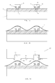
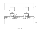
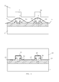
- Figures 1a to 1f illustrate the steps of the method according to a preferred embodiment of the invention.
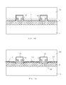
- Figure 2 illustrates a method for producing an imprinter device used in the method of the invention.
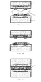
- Figure 3 illustrates the bonding process for attaching two substrates, each provided with copper bumps covered by a graphene layer.
- Figure 4 illustrates how a connection between copper bumps covered by a graphene layer can be separated.
- Figure 1a shows a substrate to which the method of the invention may be applied.
- This may be for example a silicon wafer 1 comprising one or more integrated circuits and a metallization stack for connecting said ICs to an external power source.
- the ICs and metallization are not shown in the drawing.
- a passivation layer 2 is present on top of the ICs and metallization, and metal bumps 3, preferably copper bumps are present on top of the passivation layer.
- the passivation layer may be BCB or a polyimide film for example.
- a general requirement for the passivation layer according to a preferred embodiment, is that this layer is deformable to such a degree that the imprinter device (see further) may be imprinted into the surface of this layer, i.e.
- the layer is sufficiently 'soft' for a patterned substrate to make an imprint on its surface.
- Metal connections 4 are present between at least some of the bumps 3 and the device wafer 1.
- the bumps 3 are seated on a contact pad 5, with a barrier+seed layer 6 (i.e. stack of barrier and seed layer) separating the bump from the pad and the passivation layer, the barrier layer serving to avoid copper contamination of the ICs; the seed layer serves as the basis for initiating the growth of the Cu bump.
- barrier+seed layer 6 i.e. stack of barrier and seed layer
- a graphene sheet 7 is then provided and placed over the bumps 3, see figure 1b .
- the sheet may be produced in any known manner, for example by CVD (Chemical Vapour Deposition) on a copper substrate.
- the graphene is attached to the copper bumps in the following manner.
- a specifically designed imprinter device is aligned with the wafer ( figure 1c ).
- the imprinter device consists of or comprises an imprinter substrate 10 with a pattern of cavities 11 through its front surface 9.
- the pattern of cavities corresponds to the pattern of the bumps 3, so that when the imprinter substrate 10 and the substrate 1 are aligned, each of the bumps 3 is facing one of the cavities 11.
- the cavities 11 are dimensioned so as to fit closely over the copper bumps 3 with a minimal tolerance in terms of the distance between the side walls of the cavities and the side walls of the bumps.
- the distance between the side wall of the bump 3 and the inner vertical wall of the cavity 11 may depend on the thickness of the graphene sheet.
- said distance may be twice the thickness of the graphene sheet.
- the graphene sheet may be a single layer or multiple layer sheet, which should be taken into account in designing the dimensions of the cavities with respect to the bumps.
- the invention is relevant for any bump diameter, bump height and bump pitch, ranging from a few nm to hundreds of microns (for each of the parameters diameter, height and pitch), and to any shape of the bumps.
- the sizing of the cavities is therefore dependent on each particular case, and it is within the skill of the skilled person to determine a suitable cavity size capable of arranging the graphene sheet so that it fully covers the metal bump.
- the edge of the cavities 11 is provided with a rim 12 which is protruding outward from the imprinter's front surface 9, in the direction of the bumps when the imprinter is aligned with the wafer.
- the rim 12 protrudes from the imprinter's surface 9 over a distance H1.
- the depth H2 of the cavities, measured from the bottom of the cavities to the top of the rim 12 is higher than the height of the bumps 3, as measured from the surface of the passivation layer 2.
- the imprinter substrate 10 is lowered until each of the bumps 3 is enclosed within one of the cavities 11, and the rim 12 comes into contact with the surface of the passivation layer 2.
- This causes the graphene sheet 7 to be closely arranged around the bumps.
- the rim protrusions 12 are imprinted into the surface of the passivation layer 2, see figure 1e , thereby cutting through the graphene on said surface of the passivation layer 2.
- the bottom of the cavity may come in contact with the top of the bump at the end of the imprinting step, but this is not a requirement.
- the imprinting step may be regarded as finished as soon as the graphene sheet is cut.
- graphene sheet portions 15 (hereafter also referred to as graphene layers 15) remain on top of and on the side walls of the bumps ( figure 1f ).
- the graphene layer 15 is held in place by the portion 16 which has been pushed into the passivation layer 2 by the imprinter's rim 12, i.e. the graphene portion 16 that remains on the bottom and inner side wall of the ring-shaped indentation 17 made by the rim 12 (see figures 1e and 1f ).
- the portion that is actually holding the graphene in place may be the portion at the bottom of the indentation 17 or at the sidewall of the indentation or both.
- the material of the passivation layer 2, the shape of the rim portion 12 and the imprinting force are such that this portion 16 becomes attached to the passivation layer 2 to thereby hold the graphene onto the bump when the imprinter is removed.
- the shape of the rim 12 may be designed so that it cuts through the graphene only on the outer side wall of said indentation 17.
- the loose portions 13 of the sheet can be removed by a dry or wet cleaning method, and possibly recycled for re-use in other applications.
- the manipulation of the imprinter substrate 10 with respect to the wafer may be executed as a bonding step known as such in the art. This manipulation may therefore be done in a bonding tool as known in the art, such as an EVG®520 bonder or a thermal compression bonder FC150 or FC300 from Smart Equipment Technologies.
- the imprinting step may be performed at room temperature or under high temperature, preferably in the temperature range between 25°C and 1000°C.
- the imprinting force may be anywhere between 50MPa and 1000MPa.
- the imprinter substrate 10 may be produced from any suitable material.
- the imprinter substrate may be produced from a steel substrate, by a technique known from the domain of stencil printing, e.g. by chemical etching or laser cutting.
- the imprinter substrate is produced from a silicon substrate, or a multilayer substrate, for example a silicon substrate provided with a silicon nitride passivation layer. In the latter case, it is possible to start from a blanket Si+SiN substrate and then make the cavities through the SiN layer, or from a Si-substrate into which cavities are made and then a SiN layer is deposited conformally into the cavities.
- Figure 2 illustrates a possible method for producing the imprinter substrate 10, starting from a silicon substrate 20.
- a photoresist layer 21 is coated onto the silicon substrate.
- the resist is exposed to light through a photomask 22 after which exposed resist is removed, a resist mask 23 remains and the silicon substrate is etched in the areas not covered by said mask 23.
- a patterned silicon surface is obtained, exhibiting a protruding rim 12 of height H1.
- a second resist layer 24 is deposited and patterned through a second photomask 25 to form a second resist mask 26, allowing the etching of the cavities 11 with depth H2, concentrically with the rim 12.
- H1 is smaller than H2.
- the invention is equally related to methods for bonding and de-bonding two bumps 3 of which at least one is provided with a graphene sheet.
- the bonding process may take place by aligning two substrates 30 and 31, for example two IC's or one IC and a carrier substrate, each one provided with metal bumps 3, covered by graphene layers 15, preferably produced according to the method described above.
- a layer 32 of underfill material is placed on the lower substrate 30 before the top substrate 31 is lowered onto said lower substrate so that the bumps are in contact ( figure 3b ).
- This assembly is then subjected to a curing step for hardening the underfill material to from a hardened layer 33 ( figure 3c ), preferably while exerting a contact pressure on the bumps 3.
- the assembly is further subjected to a post-bonding anneal, so that an alloy is formed between the materials of the respective bumps and/or of a solder layer applied on one or both bumps prior to bonding.
- a graphene layer 15 is applied on the bumps, however, the graphene forms a barrier for the copper diffusion that is required for forming the alloys, hence no alloys can be formed.
- the connection is made only by the contact between the two bumps, said contact being maintained by the hardened underfill layer 33 holding the bumps in place.
- the substrates 30/31 can be separated again, as illustrated in figure 4a .
- Most types of underfill material e.g. epoxy-based
- solder connection with solder balls 40, as illustrated in figure 4b .
- solder balls are known for example for establishing I/O connections between an IC and a carrier substrate, so the process for producing such a solder ball connection is not described here in detail.
- These solder balls 40 are typically present at the periphery of the substrates that are to be connected (or at least at the periphery of the smallest of the two substrates).
- the copper bumps 3 are not forming a single body through diffusion of copper, due to the presence of the graphene sheet 15. So when the solder balls 40 are heated to higher than the melting temperature of the solder material, the substrates can be separated, as illustrated in figure 4b .
- the shape of the rim portion 12 may be different from the protruding ring-shaped portion shown in the drawings.
- the rim portion may be a protruding ring with a cross-section other than a rectangular cross-section.
- the rim portion does not protrude outwards with respect to the imprinter substrate's front surface 9, but it is formed by a sufficiently sharp edge of the cavity 11, possibly in combination with a specifically patterned passivation layer 2 so that said layer forms a step feature 50 around the bumps into which the straight edge may be imprinted, to thereby cut off the graphene sheet (see figure 5 ), and attach the graphene sheet portions 15 to the passivation layer 2 by portions 16 (or at least a part of said portions 16) of said sheet.
- the description of a layer being deposited or produced 'on' another layer or substrate includes the options of
Landscapes
- Physics & Mathematics (AREA)
- General Physics & Mathematics (AREA)
- Internal Circuitry In Semiconductor Integrated Circuit Devices (AREA)
- Dicing (AREA)
- Engineering & Computer Science (AREA)
- Manufacturing & Machinery (AREA)
Abstract
Description
- The present invention is related to the field of semiconductor device packaging techniques, in particular involving bonding methods using copper contact bumps, for example for establishing a contact between a device package and a carrier substrate.
- Copper is widely used in the semiconductor industry, but copper oxidation is a critical issue and needs to be prevented. In the assembly process, Cu is used to connect chip to chip, chip to substrate as Flip Chip bump or wire for wire bonding, etc. Generally, a flux agent is added as stand alone material or embedded in the underfill to remove Cu oxidation during assembly. The use of a flux is however not preferred due to the flux residues that are hard to remove and generate reliability issues.
- A known solution to prevent copper oxidation is the use of graphene. Graphene is a 2-dimensional hexagonal ring structure which can act as a membrane to prevent oxygen molecules from penetrating into a copper surface, therefore avoiding the copper oxidation reaction. Graphene consists of sp2-bonded carbon atoms with bond length approximately 1.42 angstroms smaller than copper (2.55Å) and oxygen molecules (3.46Å).
- It is known to transfer a sheet of graphene by stamp techniques, as shown for example in 'Site-specific transfer-printing of individual graphene microscale patterns to arbitrary surfaces', Ya-Qing Bie et al, Advanced Materials 2011, 23, 3938-3943. This technique however requires a patterning step to create micro-stamps of graphene on PMMA supports and a complex transfer process involving a glass fibre controlled by a micromanipulator. Transferring larger graphene sheets to a surface is also known, as illustrated for example in 'A review of chemical vapour deposition of graphene on copper', Mattevi et al, Journal of Materials Chemistry, 2011, 21, 3324-3334. In the latter publication, transfer methods are described for transferring a sheet of graphene grown by CVD on a copper substrate, by attaching the sheet to a carrier (e.g. PMMA) and etching away the copper. The carrier allows to deposit the sheet on a substrate, after which the carrier itself is removed, e.g. by dissolving with acetone in the case of PMMA. However, when applied to the construction of a single functional microdevice, this technique will cause considerable waste of graphene material as only a small portion of the sheet is used.
- The present invention is related to a method for transferring a graphene sheet to metal contact bumps of a substrate that is to be used in a semiconductor device package, i.e. a stack of substrates connected by said contact bumps. In particular the method is relevant for copper contact bumps for which graphene forms a protective layer. According to the method of the invention, an imprinter device is used comprising an imprinter substrate, said substrate being provided with cavities, whereof each cavity is provided with a rim portion. The imprinter substrate is aligned with the substrate comprising the bumps and lowered onto said substrate so that each bump becomes enclosed by a cavity, until the rim portion of the cavities cuts through the graphene sheet, leaving graphene layer portions on top of each of bumps when the imprinter is removed. The graphene sheet is preferably attached to the substrate by imprinting it into a passivation layer surrounding the bumps. The invention is also related to an imprinter device as such, and to methods of debonding substrates of which the bumps are covered by a graphene layer.
- The invention is related to methods and devices as disclosed in the appended claims. Firstly, the invention is related to a method for transferring a sheet of graphene to a metal contact bump, comprising the steps of :
- Providing a substrate comprising one or more of said metal contact bumps on its surface, said bumps being surrounded by a passivation layer, i.e. covering an area around and immediately adjacent to each of said bumps,
- Placing a sheet of graphene on said substrate, said sheet covering said one or more bumps,
- Aligning an imprinter device with respect to said substrate, the imprinter device comprising an imprinter substrate having a front surface that is provided with one or more cavities through the front surface, each cavity being provided with a rim portion, the number of cavities being at least the same as the number of bumps, wherein aligning means that the imprinter device is positioned so that each of said bumps is aligned with one of said cavities,
- lowering the imprinter device with respect to the substrate so that each of the bumps becomes enclosed within a corresponding cavity, thereby arranging said sheet of graphene in contact with the top and side surfaces of said bump,
- pushing down the imprinter device until said rim portion cuts through the graphene sheet,
- lifting up the imprinter device, leaving a graphene sheet portion attached to said substrate and covering each of the bumps, with unattached graphene sheet portions remaining on the substrate in between the bumps,
- removing said unattached graphene sheet portions by a cleaning step.
- According to an embodiment, said rim portion is protruding outward with respect to said front surface of the imprinter substrate.
- Said metal bumps are preferably copper bumps. According to an embodiment, said rim portion of each of said cavities is pushed into the surface of the passivation layer, imprinting said rim portion into said passivation layer, and thereby attaching said graphene sheet portions to said passivation layer.
- Said substrate may be is an integrated circuit or a substrate configured for receiving a plurality of integrated circuits on its surface.
- The invention is equally related to an imprinter device suitable for use in the method of the invention. In such an imprinter device, said imprinter substrate may be a metal substrate, a silicon substrate or a silicon substrate with a silicon nitride layer provided on said silicon substrate.
- The invention is equally related to a method for debonding a stack of two substrates, each substrate being provided with metal contact bumps, wherein the bumps of at least one substrate are covered with a graphene sheet portion, and wherein the bumps of one substrate are in contact with the bumps of the other substrate, and wherein the two substrates are held together by a removable bonding means, said de-bonding method consisting in removing said bonding means, whereby contact between said contact bumps is released and the two substrates are fully separated.
- In the method for debonding according to the invention, said bonding means may be a cured underfill layer, and wherein the step of removing the bonding means consists of dissolving said cured underfill layer.
- Alternatively, said bonding means may be a plurality of solidified solder balls, and wherein the step of removing the bonding means consists of heating and melting said solder balls.
-
Figures 1a to 1f illustrate the steps of the method according to a preferred embodiment of the invention. -
Figure 2 illustrates a method for producing an imprinter device used in the method of the invention. -
Figure 3 illustrates the bonding process for attaching two substrates, each provided with copper bumps covered by a graphene layer. -
Figure 4 illustrates how a connection between copper bumps covered by a graphene layer can be separated. -
Figure 1a shows a substrate to which the method of the invention may be applied. This may be for example asilicon wafer 1 comprising one or more integrated circuits and a metallization stack for connecting said ICs to an external power source. The ICs and metallization are not shown in the drawing. Apassivation layer 2 is present on top of the ICs and metallization, andmetal bumps 3, preferably copper bumps are present on top of the passivation layer. The passivation layer may be BCB or a polyimide film for example. A general requirement for the passivation layer according to a preferred embodiment, is that this layer is deformable to such a degree that the imprinter device (see further) may be imprinted into the surface of this layer, i.e. the layer is sufficiently 'soft' for a patterned substrate to make an imprint on its surface.Metal connections 4 are present between at least some of thebumps 3 and the device wafer 1. Thebumps 3 are seated on acontact pad 5, with a barrier+seed layer 6 (i.e. stack of barrier and seed layer) separating the bump from the pad and the passivation layer, the barrier layer serving to avoid copper contamination of the ICs; the seed layer serves as the basis for initiating the growth of the Cu bump. These elements as such are known in the art, as are the processes and materials suitable for producing them. A preferred process for fabricating the structure offigure 1a useselectroplated bumps 3 deposited on thepads 5 after first applying and patterning a resist layer by standard photolithography. - A
graphene sheet 7 is then provided and placed over thebumps 3, seefigure 1b . The sheet may be produced in any known manner, for example by CVD (Chemical Vapour Deposition) on a copper substrate. - According to the invention, the graphene is attached to the copper bumps in the following manner. A specifically designed imprinter device is aligned with the wafer (
figure 1c ). The imprinter device consists of or comprises animprinter substrate 10 with a pattern ofcavities 11 through itsfront surface 9. The pattern of cavities corresponds to the pattern of thebumps 3, so that when theimprinter substrate 10 and thesubstrate 1 are aligned, each of thebumps 3 is facing one of thecavities 11. According to the preferred embodiment, thecavities 11 are dimensioned so as to fit closely over thecopper bumps 3 with a minimal tolerance in terms of the distance between the side walls of the cavities and the side walls of the bumps. - The distance between the side wall of the
bump 3 and the inner vertical wall of thecavity 11 may depend on the thickness of the graphene sheet. For example, said distance may be twice the thickness of the graphene sheet. The graphene sheet may be a single layer or multiple layer sheet, which should be taken into account in designing the dimensions of the cavities with respect to the bumps. The invention is relevant for any bump diameter, bump height and bump pitch, ranging from a few nm to hundreds of microns (for each of the parameters diameter, height and pitch), and to any shape of the bumps. The sizing of the cavities is therefore dependent on each particular case, and it is within the skill of the skilled person to determine a suitable cavity size capable of arranging the graphene sheet so that it fully covers the metal bump. - The edge of the
cavities 11 is provided with arim 12 which is protruding outward from the imprinter'sfront surface 9, in the direction of the bumps when the imprinter is aligned with the wafer. Therim 12 protrudes from the imprinter'ssurface 9 over a distance H1. The depth H2 of the cavities, measured from the bottom of the cavities to the top of therim 12 is higher than the height of thebumps 3, as measured from the surface of thepassivation layer 2. - As shown in
figure 1d , theimprinter substrate 10 is lowered until each of thebumps 3 is enclosed within one of thecavities 11, and therim 12 comes into contact with the surface of thepassivation layer 2. This causes thegraphene sheet 7 to be closely arranged around the bumps. By further exerting a force on the imprinter substrate, therim protrusions 12 are imprinted into the surface of thepassivation layer 2, seefigure 1e , thereby cutting through the graphene on said surface of thepassivation layer 2. The bottom of the cavity may come in contact with the top of the bump at the end of the imprinting step, but this is not a requirement. The imprinting step may be regarded as finished as soon as the graphene sheet is cut. -
Loose portions 13 of the sheet remain on the surface of thepassivation layer 2. When the imprinter is lifted again, graphene sheet portions 15 (hereafter also referred to as graphene layers 15) remain on top of and on the side walls of the bumps (figure 1f ). According to an embodiment, thegraphene layer 15 is held in place by theportion 16 which has been pushed into thepassivation layer 2 by the imprinter'srim 12, i.e. thegraphene portion 16 that remains on the bottom and inner side wall of the ring-shapedindentation 17 made by the rim 12 (seefigures 1e and1f ). The portion that is actually holding the graphene in place may be the portion at the bottom of theindentation 17 or at the sidewall of the indentation or both. The material of thepassivation layer 2, the shape of therim portion 12 and the imprinting force are such that thisportion 16 becomes attached to thepassivation layer 2 to thereby hold the graphene onto the bump when the imprinter is removed. The shape of therim 12 may be designed so that it cuts through the graphene only on the outer side wall of saidindentation 17. Theloose portions 13 of the sheet can be removed by a dry or wet cleaning method, and possibly recycled for re-use in other applications. - The manipulation of the
imprinter substrate 10 with respect to the wafer, hereafter referred to as the imprinting step, may be executed as a bonding step known as such in the art. This manipulation may therefore be done in a bonding tool as known in the art, such as an EVG®520 bonder or a thermal compression bonder FC150 or FC300 from Smart Equipment Technologies. The imprinting step may be performed at room temperature or under high temperature, preferably in the temperature range between 25°C and 1000°C. The imprinting force may be anywhere between 50MPa and 1000MPa. - The
imprinter substrate 10 may be produced from any suitable material. For example, the imprinter substrate may be produced from a steel substrate, by a technique known from the domain of stencil printing, e.g. by chemical etching or laser cutting. According to another embodiment, the imprinter substrate is produced from a silicon substrate, or a multilayer substrate, for example a silicon substrate provided with a silicon nitride passivation layer. In the latter case, it is possible to start from a blanket Si+SiN substrate and then make the cavities through the SiN layer, or from a Si-substrate into which cavities are made and then a SiN layer is deposited conformally into the cavities. -
Figure 2 illustrates a possible method for producing theimprinter substrate 10, starting from asilicon substrate 20. After a pre-cleaning step, aphotoresist layer 21 is coated onto the silicon substrate. The resist is exposed to light through aphotomask 22 after which exposed resist is removed, a resistmask 23 remains and the silicon substrate is etched in the areas not covered by saidmask 23. After stripping the resist mask, a patterned silicon surface is obtained, exhibiting a protrudingrim 12 of height H1. Then, a second resistlayer 24 is deposited and patterned through asecond photomask 25 to form a second resistmask 26, allowing the etching of thecavities 11 with depth H2, concentrically with therim 12. According to a preferred embodiment, H1 is smaller than H2. - The invention is equally related to methods for bonding and de-bonding two
bumps 3 of which at least one is provided with a graphene sheet. As shown infigure 3a , the bonding process may take place by aligning twosubstrates metal bumps 3, covered bygraphene layers 15, preferably produced according to the method described above. Alayer 32 of underfill material is placed on thelower substrate 30 before thetop substrate 31 is lowered onto said lower substrate so that the bumps are in contact (figure 3b ). This assembly is then subjected to a curing step for hardening the underfill material to from a hardened layer 33 (figure 3c ), preferably while exerting a contact pressure on thebumps 3. When no graphene layer is present, the assembly is further subjected to a post-bonding anneal, so that an alloy is formed between the materials of the respective bumps and/or of a solder layer applied on one or both bumps prior to bonding. When agraphene layer 15 is applied on the bumps, however, the graphene forms a barrier for the copper diffusion that is required for forming the alloys, hence no alloys can be formed. In other words, the connection is made only by the contact between the two bumps, said contact being maintained by thehardened underfill layer 33 holding the bumps in place. This means that when the underfill material is removed, thesubstrates 30/31 can be separated again, as illustrated infigure 4a . Most types of underfill material (e.g. epoxy-based) can be removed by dissolving the material. This may be useful for example when the substrates need to be separated for repair purposes. - An alternative for establishing the connection between two
substrates copper bumps 3 is a solder connection withsolder balls 40, as illustrated infigure 4b . Such solder balls are known for example for establishing I/O connections between an IC and a carrier substrate, so the process for producing such a solder ball connection is not described here in detail. Thesesolder balls 40 are typically present at the periphery of the substrates that are to be connected (or at least at the periphery of the smallest of the two substrates). Again, the copper bumps 3 are not forming a single body through diffusion of copper, due to the presence of thegraphene sheet 15. So when thesolder balls 40 are heated to higher than the melting temperature of the solder material, the substrates can be separated, as illustrated infigure 4b . - Some alternatives of the above-described embodiments are included in the scope of the invention. In stead of a
single sheet 7 of graphene, a smaller sheet of graphene may be placed over eachbump 3 separately. - The shape of the
rim portion 12 may be different from the protruding ring-shaped portion shown in the drawings. The rim portion may be a protruding ring with a cross-section other than a rectangular cross-section. According to an embodiment, the rim portion does not protrude outwards with respect to the imprinter substrate'sfront surface 9, but it is formed by a sufficiently sharp edge of thecavity 11, possibly in combination with a specifically patternedpassivation layer 2 so that said layer forms astep feature 50 around the bumps into which the straight edge may be imprinted, to thereby cut off the graphene sheet (seefigure 5 ), and attach thegraphene sheet portions 15 to thepassivation layer 2 by portions 16 (or at least a part of said portions 16) of said sheet. - While the invention has been illustrated and described in detail in the drawings and foregoing description, such illustration and description are to be considered illustrative or exemplary and not restrictive. Other variations to the disclosed embodiments can be understood and effected by those skilled in the art in practicing the claimed invention, from a study of the drawings, the disclosure and the appended claims. In the claims, the word "comprising" does not exclude other elements or steps, and the indefinite article "a" or "an" does not exclude a plurality. The mere fact that certain measures are recited in mutually different dependent claims does not indicate that a combination of these measures cannot be used to advantage. Any reference signs in the claims should not be construed as limiting the scope.
- The foregoing description details certain embodiments of the invention. It will be appreciated, however, that no matter how detailed the foregoing appears in text, the invention may be practiced in many ways, and is therefore not limited to the embodiments disclosed. It should be noted that the use of particular terminology when describing certain features or aspects of the invention should not be taken to imply that the terminology is being re-defined herein to be restricted to include any specific characteristics of the features or aspects of the invention with which that terminology is associated.
- Unless specifically specified, the description of a layer being deposited or produced 'on' another layer or substrate, includes the options of
- • said layer being produced or deposited directly on, i.e. in contact with, said other layer or substrate, and
Claims (10)
- A method for transferring a sheet of graphene (7) to a metal contact bump (3), comprising the steps of :- Providing a substrate (1) comprising one or more of said metal contact bumps (3) on its surface, said bumps being surrounded by a passivation layer (2),- Placing a sheet (7) of graphene on said substrate, said sheet covering said one or more bumps (3),- Aligning an imprinter device with respect to said substrate, the imprinter device comprising an imprinter substrate (10) having a front surface (9) that is provided with one or more cavities (11) through the front surface, each cavity being provided with a rim portion (12), the number of cavities being at least the same as the number of bumps (3), wherein aligning means that the imprinter device is positioned so that each of said bumps (3) is aligned with one of said cavities (11),- lowering the imprinter device with respect to the substrate so that each of the bumps (3) becomes enclosed within a corresponding cavity (11), thereby arranging said sheet (7) of graphene in contact with the top and side surfaces of said bump (3),- pushing down the imprinter device until said rim portion (12) cuts through the graphene sheet (7),- lifting up the imprinter device, leaving a graphene sheet portion (15) attached to said substrate (1) and covering each of the bumps (3), with unattached graphene sheet portions (13) remaining on the substrate in between the bumps (3),- removing said unattached graphene sheet portions (13) by a cleaning step.
- Method according to claim 1, wherein said rim portion (12) is protruding outward with respect to said front surface (9) of the imprinter substrate.
- Method according to claim 1 or 2, wherein said metal bumps (3) are copper bumps.
- Method according to claim 1, 2 or 3, wherein said rim portion (12) of each of said cavities (11) is pushed into the surface of the passivation layer (2), imprinting said rim portion into said passivation layer, and thereby attaching said graphene sheet portions (15) to said passivation layer (2).
- Method according to any one of claims 1 to 4, wherein said substrate (1) is an integrated circuit or a substrate configured for receiving a plurality of integrated circuits on its surface.
- Imprinter device for use in the method according to any one of claims 1 to 5.
- Imprinter device according to claim 6, wherein said imprinter substrate (10) is a metal substrate, a silicon substrate or a silicon substrate with a silicon nitride layer provided on said silicon substrate.
- Method for debonding a stack of two substrates (30,31), each substrate being provided with metal contact bumps (3), wherein the bumps of at least one substrate are covered with a graphene sheet portion (15), and wherein the bumps of one substrate are in contact with the bumps of the other substrate, and wherein the two substrates are held together by a removable bonding means, said de-bonding method consisting in removing said bonding means, whereby contact between said contact bumps is released and the two substrates are fully separated.
- Method according to claim 8, wherein said bonding means is a cured underfill layer (33), and wherein the step of removing the bonding means consists of dissolving said cured underfill layer (33).
- Method according to claim 9, wherein said bonding means is a plurality of solidified solder balls (40), and wherein the step of removing the bonding means consists of heating and melting said solder balls (40).
Priority Applications (4)
| Application Number | Priority Date | Filing Date | Title |
|---|---|---|---|
| EP12197820.9A EP2747132B1 (en) | 2012-12-18 | 2012-12-18 | A method for transferring a graphene sheet to metal contact bumps of a substrate for use in semiconductor device package |
| US14/089,612 US8974617B2 (en) | 2012-12-18 | 2013-11-25 | Method for transferring a graphene sheet to metal contact bumps of a substrate for use in semiconductor device package |
| JP2013244596A JP2014120767A (en) | 2012-12-18 | 2013-11-27 | Method for transferring graphene sheet to metal contact bumps of substrate for use in semiconductor device package |
| CN201310692838.7A CN103871909A (en) | 2012-12-18 | 2013-12-17 | Method for transferring graphene sheets to substrate metal contact bumps for packaging |
Applications Claiming Priority (1)
| Application Number | Priority Date | Filing Date | Title |
|---|---|---|---|
| EP12197820.9A EP2747132B1 (en) | 2012-12-18 | 2012-12-18 | A method for transferring a graphene sheet to metal contact bumps of a substrate for use in semiconductor device package |
Publications (2)
| Publication Number | Publication Date |
|---|---|
| EP2747132A1 true EP2747132A1 (en) | 2014-06-25 |
| EP2747132B1 EP2747132B1 (en) | 2018-11-21 |
Family
ID=47664061
Family Applications (1)
| Application Number | Title | Priority Date | Filing Date |
|---|---|---|---|
| EP12197820.9A Active EP2747132B1 (en) | 2012-12-18 | 2012-12-18 | A method for transferring a graphene sheet to metal contact bumps of a substrate for use in semiconductor device package |
Country Status (4)
| Country | Link |
|---|---|
| US (1) | US8974617B2 (en) |
| EP (1) | EP2747132B1 (en) |
| JP (1) | JP2014120767A (en) |
| CN (1) | CN103871909A (en) |
Families Citing this family (10)
| Publication number | Priority date | Publication date | Assignee | Title |
|---|---|---|---|---|
| US10833033B2 (en) * | 2011-07-27 | 2020-11-10 | Taiwan Semiconductor Manufacturing Co., Ltd. | Bump structure having a side recess and semiconductor structure including the same |
| JP6335099B2 (en) | 2014-11-04 | 2018-05-30 | 東芝メモリ株式会社 | Semiconductor device and manufacturing method of semiconductor device |
| US10074625B2 (en) * | 2015-09-20 | 2018-09-11 | Qualcomm Incorporated | Wafer level package (WLP) ball support using cavity structure |
| KR20170065953A (en) * | 2015-12-04 | 2017-06-14 | 삼성전기주식회사 | Antenna pattern frame and method for manufacturing case of electronic device having the same |
| CN105405826B (en) * | 2015-12-23 | 2019-02-15 | 中芯长电半导体(江阴)有限公司 | A copper pillar bump package structure and its manufacturing method |
| CN107993928B (en) * | 2017-11-20 | 2020-05-12 | 长江存储科技有限责任公司 | A method for suppressing copper electromigration in wafer hybrid bonding |
| CN111326503B (en) * | 2019-12-31 | 2021-03-12 | 诺思(天津)微系统有限责任公司 | Semiconductor structure with stacked units, manufacturing method and electronic equipment |
| CN113104809B (en) * | 2021-04-08 | 2024-07-02 | 德州学院 | Method for preparing graphene nano-network by utilizing patterned substrate imprinting |
| CN116344350A (en) * | 2021-12-24 | 2023-06-27 | 慧隆科技股份有限公司 | Flip-chip package structure and manufacturing method thereof |
| US11955443B2 (en) * | 2022-02-17 | 2024-04-09 | Amazing Cool Technology Corp. | Flip chip package structure and manufacturing method thereof |
Citations (6)
| Publication number | Priority date | Publication date | Assignee | Title |
|---|---|---|---|---|
| WO2002011202A2 (en) * | 2000-07-31 | 2002-02-07 | Siemens Dematic Ag | Method and device for producing connection substrates for electronic components |
| US20080169563A1 (en) * | 2005-03-17 | 2008-07-17 | Fujitsu Limited | Semiconductor package and method of manufacturing the same |
| WO2009158552A1 (en) * | 2008-06-26 | 2009-12-30 | Carben Semicon Limited | Patterned integrated circuit and method of production thereof |
| US20100075493A1 (en) * | 2008-09-24 | 2010-03-25 | Fujitsu Limited | Method of forming electrode connecting portion |
| US20110032684A1 (en) * | 2009-08-07 | 2011-02-10 | Semiconductor Energy Laboratory Co., Ltd. | Terminal structure and manufacturing method thereof, and electronic device and manufacturing method thereof |
| US20110233767A1 (en) * | 2010-03-29 | 2011-09-29 | Panasonic Corporation | Semiconductor device and semiconductor device manufacturing method |
Family Cites Families (3)
| Publication number | Priority date | Publication date | Assignee | Title |
|---|---|---|---|---|
| DE102007035902A1 (en) * | 2007-07-31 | 2009-02-05 | Siemens Ag | Method for producing an electronic component and electronic component |
| KR101501599B1 (en) | 2008-10-27 | 2015-03-11 | 삼성전자주식회사 | Method for removing carbonization catalyst from graphene sheet and method for transferring graphene sheet |
| CN103454855B (en) * | 2008-12-04 | 2015-08-19 | Asml荷兰有限公司 | The impressing mould of imprint lithography, equipment and patterning method |
-
2012
- 2012-12-18 EP EP12197820.9A patent/EP2747132B1/en active Active
-
2013
- 2013-11-25 US US14/089,612 patent/US8974617B2/en active Active
- 2013-11-27 JP JP2013244596A patent/JP2014120767A/en active Pending
- 2013-12-17 CN CN201310692838.7A patent/CN103871909A/en active Pending
Patent Citations (6)
| Publication number | Priority date | Publication date | Assignee | Title |
|---|---|---|---|---|
| WO2002011202A2 (en) * | 2000-07-31 | 2002-02-07 | Siemens Dematic Ag | Method and device for producing connection substrates for electronic components |
| US20080169563A1 (en) * | 2005-03-17 | 2008-07-17 | Fujitsu Limited | Semiconductor package and method of manufacturing the same |
| WO2009158552A1 (en) * | 2008-06-26 | 2009-12-30 | Carben Semicon Limited | Patterned integrated circuit and method of production thereof |
| US20100075493A1 (en) * | 2008-09-24 | 2010-03-25 | Fujitsu Limited | Method of forming electrode connecting portion |
| US20110032684A1 (en) * | 2009-08-07 | 2011-02-10 | Semiconductor Energy Laboratory Co., Ltd. | Terminal structure and manufacturing method thereof, and electronic device and manufacturing method thereof |
| US20110233767A1 (en) * | 2010-03-29 | 2011-09-29 | Panasonic Corporation | Semiconductor device and semiconductor device manufacturing method |
Non-Patent Citations (2)
| Title |
|---|
| MATTEVI ET AL., JOURNAL OF MATERIALS CHEMISTRY, vol. 21, 2011, pages 3324 - 3334 |
| YA-QING BIE ET AL., ADVANCED MATERIALS, vol. 23, 2011, pages 3938 - 3943 |
Also Published As
| Publication number | Publication date |
|---|---|
| JP2014120767A (en) | 2014-06-30 |
| CN103871909A (en) | 2014-06-18 |
| EP2747132B1 (en) | 2018-11-21 |
| US20140166194A1 (en) | 2014-06-19 |
| US8974617B2 (en) | 2015-03-10 |
Similar Documents
| Publication | Publication Date | Title |
|---|---|---|
| EP2747132B1 (en) | A method for transferring a graphene sheet to metal contact bumps of a substrate for use in semiconductor device package | |
| US9786628B2 (en) | Air trench in packages incorporating hybrid bonding | |
| CN102290367B (en) | Method and apparatus for removing reversibly mounted device wafer from carrier substrate | |
| CN101652847B (en) | Electrical interconnect structure and method of forming same | |
| JP4559993B2 (en) | Manufacturing method of semiconductor device | |
| US8642391B2 (en) | Self-assembly of chips on a substrate | |
| TW201125097A (en) | Chip package | |
| JP2013168594A (en) | Semiconductor device manufacturing method and electronic apparatus manufacturing method | |
| JP5903920B2 (en) | Semiconductor device manufacturing method and electronic device manufacturing method | |
| JP5810958B2 (en) | Semiconductor device manufacturing method and electronic device manufacturing method | |
| TW201334956A (en) | Manufacturing method of wiring board, manufacturing method of supporting member of wiring board, and structure of wiring board | |
| TW201142999A (en) | Chip package and fabrication method thereof | |
| WO2011032647A1 (en) | Method for chip to wafer bonding | |
| CN110349912A (en) | A method of for semiconductor subassembly to be coupled to target substrate by transferring | |
| CN105575889A (en) | Method for manufacturing three-dimensional integrated circuit | |
| CN104779232B (en) | Pass through the encapsulation of pre-formed metal pins | |
| EP2572380B1 (en) | Method for producing chip stacks and a carrier for carrying out the method | |
| EP3029725B1 (en) | Chuck for collective bonding of semiconductor dies, method of making the same and methods of using the same | |
| CN111341763A (en) | Low cost reliable fan-out fan-in chip scale package | |
| JP7705209B2 (en) | Transferable pillar structure for fan-out package or interconnect bridge | |
| JP2010147418A (en) | Semiconductor device and method of manufacturing same | |
| TW201407693A (en) | Mounting method | |
| TWI668771B (en) | Method for manufacturing chip package | |
| KR102937902B1 (en) | De-Lamination apparatus | |
| TW202603987A (en) | Decomposable polymer in microsolid printing process |
Legal Events
| Date | Code | Title | Description |
|---|---|---|---|
| PUAI | Public reference made under article 153(3) epc to a published international application that has entered the european phase |
Free format text: ORIGINAL CODE: 0009012 |
|
| 17P | Request for examination filed |
Effective date: 20121218 |
|
| AK | Designated contracting states |
Kind code of ref document: A1 Designated state(s): AL AT BE BG CH CY CZ DE DK EE ES FI FR GB GR HR HU IE IS IT LI LT LU LV MC MK MT NL NO PL PT RO RS SE SI SK SM TR |
|
| AX | Request for extension of the european patent |
Extension state: BA ME |
|
| R17P | Request for examination filed (corrected) |
Effective date: 20141212 |
|
| RBV | Designated contracting states (corrected) |
Designated state(s): AL AT BE BG CH CY CZ DE DK EE ES FI FR GB GR HR HU IE IS IT LI LT LU LV MC MK MT NL NO PL PT RO RS SE SI SK SM TR |
|
| RAP1 | Party data changed (applicant data changed or rights of an application transferred) |
Owner name: IMEC VZW Owner name: TAIWAN SEMICONDUCTOR MANUFACTURING COMPANY, LTD. ( |
|
| GRAP | Despatch of communication of intention to grant a patent |
Free format text: ORIGINAL CODE: EPIDOSNIGR1 |
|
| INTG | Intention to grant announced |
Effective date: 20180618 |
|
| GRAS | Grant fee paid |
Free format text: ORIGINAL CODE: EPIDOSNIGR3 |
|
| GRAA | (expected) grant |
Free format text: ORIGINAL CODE: 0009210 |
|
| AK | Designated contracting states |
Kind code of ref document: B1 Designated state(s): AL AT BE BG CH CY CZ DE DK EE ES FI FR GB GR HR HU IE IS IT LI LT LU LV MC MK MT NL NO PL PT RO RS SE SI SK SM TR |
|
| REG | Reference to a national code |
Ref country code: CH Ref legal event code: EP |
|
| REG | Reference to a national code |
Ref country code: IE Ref legal event code: FG4D |
|
| REG | Reference to a national code |
Ref country code: DE Ref legal event code: R096 Ref document number: 602012053729 Country of ref document: DE |
|
| REG | Reference to a national code |
Ref country code: AT Ref legal event code: REF Ref document number: 1068525 Country of ref document: AT Kind code of ref document: T Effective date: 20181215 |
|
| REG | Reference to a national code |
Ref country code: NL Ref legal event code: MP Effective date: 20181121 |
|
| REG | Reference to a national code |
Ref country code: AT Ref legal event code: MK05 Ref document number: 1068525 Country of ref document: AT Kind code of ref document: T Effective date: 20181121 |
|
| PG25 | Lapsed in a contracting state [announced via postgrant information from national office to epo] |
Ref country code: NO Free format text: LAPSE BECAUSE OF FAILURE TO SUBMIT A TRANSLATION OF THE DESCRIPTION OR TO PAY THE FEE WITHIN THE PRESCRIBED TIME-LIMIT Effective date: 20190221 Ref country code: LT Free format text: LAPSE BECAUSE OF FAILURE TO SUBMIT A TRANSLATION OF THE DESCRIPTION OR TO PAY THE FEE WITHIN THE PRESCRIBED TIME-LIMIT Effective date: 20181121 Ref country code: HR Free format text: LAPSE BECAUSE OF FAILURE TO SUBMIT A TRANSLATION OF THE DESCRIPTION OR TO PAY THE FEE WITHIN THE PRESCRIBED TIME-LIMIT Effective date: 20181121 Ref country code: BG Free format text: LAPSE BECAUSE OF FAILURE TO SUBMIT A TRANSLATION OF THE DESCRIPTION OR TO PAY THE FEE WITHIN THE PRESCRIBED TIME-LIMIT Effective date: 20190221 Ref country code: FI Free format text: LAPSE BECAUSE OF FAILURE TO SUBMIT A TRANSLATION OF THE DESCRIPTION OR TO PAY THE FEE WITHIN THE PRESCRIBED TIME-LIMIT Effective date: 20181121 Ref country code: LV Free format text: LAPSE BECAUSE OF FAILURE TO SUBMIT A TRANSLATION OF THE DESCRIPTION OR TO PAY THE FEE WITHIN THE PRESCRIBED TIME-LIMIT Effective date: 20181121 Ref country code: ES Free format text: LAPSE BECAUSE OF FAILURE TO SUBMIT A TRANSLATION OF THE DESCRIPTION OR TO PAY THE FEE WITHIN THE PRESCRIBED TIME-LIMIT Effective date: 20181121 Ref country code: IS Free format text: LAPSE BECAUSE OF FAILURE TO SUBMIT A TRANSLATION OF THE DESCRIPTION OR TO PAY THE FEE WITHIN THE PRESCRIBED TIME-LIMIT Effective date: 20190321 Ref country code: AT Free format text: LAPSE BECAUSE OF FAILURE TO SUBMIT A TRANSLATION OF THE DESCRIPTION OR TO PAY THE FEE WITHIN THE PRESCRIBED TIME-LIMIT Effective date: 20181121 |
|
| PG25 | Lapsed in a contracting state [announced via postgrant information from national office to epo] |
Ref country code: PT Free format text: LAPSE BECAUSE OF FAILURE TO SUBMIT A TRANSLATION OF THE DESCRIPTION OR TO PAY THE FEE WITHIN THE PRESCRIBED TIME-LIMIT Effective date: 20190321 Ref country code: NL Free format text: LAPSE BECAUSE OF FAILURE TO SUBMIT A TRANSLATION OF THE DESCRIPTION OR TO PAY THE FEE WITHIN THE PRESCRIBED TIME-LIMIT Effective date: 20181121 Ref country code: GR Free format text: LAPSE BECAUSE OF FAILURE TO SUBMIT A TRANSLATION OF THE DESCRIPTION OR TO PAY THE FEE WITHIN THE PRESCRIBED TIME-LIMIT Effective date: 20190222 Ref country code: RS Free format text: LAPSE BECAUSE OF FAILURE TO SUBMIT A TRANSLATION OF THE DESCRIPTION OR TO PAY THE FEE WITHIN THE PRESCRIBED TIME-LIMIT Effective date: 20181121 Ref country code: AL Free format text: LAPSE BECAUSE OF FAILURE TO SUBMIT A TRANSLATION OF THE DESCRIPTION OR TO PAY THE FEE WITHIN THE PRESCRIBED TIME-LIMIT Effective date: 20181121 Ref country code: SE Free format text: LAPSE BECAUSE OF FAILURE TO SUBMIT A TRANSLATION OF THE DESCRIPTION OR TO PAY THE FEE WITHIN THE PRESCRIBED TIME-LIMIT Effective date: 20181121 |
|
| PG25 | Lapsed in a contracting state [announced via postgrant information from national office to epo] |
Ref country code: PL Free format text: LAPSE BECAUSE OF FAILURE TO SUBMIT A TRANSLATION OF THE DESCRIPTION OR TO PAY THE FEE WITHIN THE PRESCRIBED TIME-LIMIT Effective date: 20181121 Ref country code: DK Free format text: LAPSE BECAUSE OF FAILURE TO SUBMIT A TRANSLATION OF THE DESCRIPTION OR TO PAY THE FEE WITHIN THE PRESCRIBED TIME-LIMIT Effective date: 20181121 Ref country code: IT Free format text: LAPSE BECAUSE OF FAILURE TO SUBMIT A TRANSLATION OF THE DESCRIPTION OR TO PAY THE FEE WITHIN THE PRESCRIBED TIME-LIMIT Effective date: 20181121 Ref country code: CZ Free format text: LAPSE BECAUSE OF FAILURE TO SUBMIT A TRANSLATION OF THE DESCRIPTION OR TO PAY THE FEE WITHIN THE PRESCRIBED TIME-LIMIT Effective date: 20181121 |
|
| REG | Reference to a national code |
Ref country code: CH Ref legal event code: PL |
|
| REG | Reference to a national code |
Ref country code: DE Ref legal event code: R097 Ref document number: 602012053729 Country of ref document: DE |
|
| PG25 | Lapsed in a contracting state [announced via postgrant information from national office to epo] |
Ref country code: MC Free format text: LAPSE BECAUSE OF FAILURE TO SUBMIT A TRANSLATION OF THE DESCRIPTION OR TO PAY THE FEE WITHIN THE PRESCRIBED TIME-LIMIT Effective date: 20181121 Ref country code: LU Free format text: LAPSE BECAUSE OF NON-PAYMENT OF DUE FEES Effective date: 20181218 Ref country code: SK Free format text: LAPSE BECAUSE OF FAILURE TO SUBMIT A TRANSLATION OF THE DESCRIPTION OR TO PAY THE FEE WITHIN THE PRESCRIBED TIME-LIMIT Effective date: 20181121 Ref country code: SM Free format text: LAPSE BECAUSE OF FAILURE TO SUBMIT A TRANSLATION OF THE DESCRIPTION OR TO PAY THE FEE WITHIN THE PRESCRIBED TIME-LIMIT Effective date: 20181121 Ref country code: EE Free format text: LAPSE BECAUSE OF FAILURE TO SUBMIT A TRANSLATION OF THE DESCRIPTION OR TO PAY THE FEE WITHIN THE PRESCRIBED TIME-LIMIT Effective date: 20181121 Ref country code: RO Free format text: LAPSE BECAUSE OF FAILURE TO SUBMIT A TRANSLATION OF THE DESCRIPTION OR TO PAY THE FEE WITHIN THE PRESCRIBED TIME-LIMIT Effective date: 20181121 |
|
| REG | Reference to a national code |
Ref country code: IE Ref legal event code: MM4A |
|
| PLBE | No opposition filed within time limit |
Free format text: ORIGINAL CODE: 0009261 |
|
| STAA | Information on the status of an ep patent application or granted ep patent |
Free format text: STATUS: NO OPPOSITION FILED WITHIN TIME LIMIT |
|
| REG | Reference to a national code |
Ref country code: BE Ref legal event code: MM Effective date: 20181231 |
|
| GBPC | Gb: european patent ceased through non-payment of renewal fee |
Effective date: 20190221 |
|
| 26N | No opposition filed |
Effective date: 20190822 |
|
| PG25 | Lapsed in a contracting state [announced via postgrant information from national office to epo] |
Ref country code: SI Free format text: LAPSE BECAUSE OF FAILURE TO SUBMIT A TRANSLATION OF THE DESCRIPTION OR TO PAY THE FEE WITHIN THE PRESCRIBED TIME-LIMIT Effective date: 20181121 Ref country code: IE Free format text: LAPSE BECAUSE OF NON-PAYMENT OF DUE FEES Effective date: 20181218 |
|
| PG25 | Lapsed in a contracting state [announced via postgrant information from national office to epo] |
Ref country code: BE Free format text: LAPSE BECAUSE OF NON-PAYMENT OF DUE FEES Effective date: 20181231 |
|
| PG25 | Lapsed in a contracting state [announced via postgrant information from national office to epo] |
Ref country code: CH Free format text: LAPSE BECAUSE OF NON-PAYMENT OF DUE FEES Effective date: 20181231 Ref country code: LI Free format text: LAPSE BECAUSE OF NON-PAYMENT OF DUE FEES Effective date: 20181231 |
|
| PG25 | Lapsed in a contracting state [announced via postgrant information from national office to epo] |
Ref country code: MT Free format text: LAPSE BECAUSE OF NON-PAYMENT OF DUE FEES Effective date: 20181218 Ref country code: GB Free format text: LAPSE BECAUSE OF NON-PAYMENT OF DUE FEES Effective date: 20190221 |
|
| PG25 | Lapsed in a contracting state [announced via postgrant information from national office to epo] |
Ref country code: TR Free format text: LAPSE BECAUSE OF FAILURE TO SUBMIT A TRANSLATION OF THE DESCRIPTION OR TO PAY THE FEE WITHIN THE PRESCRIBED TIME-LIMIT Effective date: 20181121 |
|
| PG25 | Lapsed in a contracting state [announced via postgrant information from national office to epo] |
Ref country code: CY Free format text: LAPSE BECAUSE OF FAILURE TO SUBMIT A TRANSLATION OF THE DESCRIPTION OR TO PAY THE FEE WITHIN THE PRESCRIBED TIME-LIMIT Effective date: 20181121 Ref country code: HU Free format text: LAPSE BECAUSE OF FAILURE TO SUBMIT A TRANSLATION OF THE DESCRIPTION OR TO PAY THE FEE WITHIN THE PRESCRIBED TIME-LIMIT; INVALID AB INITIO Effective date: 20121218 Ref country code: MK Free format text: LAPSE BECAUSE OF NON-PAYMENT OF DUE FEES Effective date: 20181121 |
|
| REG | Reference to a national code |
Ref country code: DE Ref legal event code: R081 Ref document number: 602012053729 Country of ref document: DE Owner name: TAIWAN SEMICONDUCTOR MANUFACTURING COMPANY, LT, TW Free format text: FORMER OWNERS: IMEC VZW, LEUVEN, BE; TAIWAN SEMICONDUCTOR MANUFACTURING COMPANY, LTD., HSINCHU, TW |
|
| P01 | Opt-out of the competence of the unified patent court (upc) registered |
Effective date: 20230513 |
|
| REG | Reference to a national code |
Ref country code: DE Ref legal event code: R079 Ref document number: 602012053729 Country of ref document: DE Free format text: PREVIOUS MAIN CLASS: H01L0023000000 Ipc: H10W0099000000 |
|
| PGFP | Annual fee paid to national office [announced via postgrant information from national office to epo] |
Ref country code: FR Payment date: 20251226 Year of fee payment: 14 |
|
| PGFP | Annual fee paid to national office [announced via postgrant information from national office to epo] |
Ref country code: DE Payment date: 20251229 Year of fee payment: 14 |