EP2744109A1 - Pulse generator circuit - Google Patents
Pulse generator circuit Download PDFInfo
- Publication number
- EP2744109A1 EP2744109A1 EP13197356.2A EP13197356A EP2744109A1 EP 2744109 A1 EP2744109 A1 EP 2744109A1 EP 13197356 A EP13197356 A EP 13197356A EP 2744109 A1 EP2744109 A1 EP 2744109A1
- Authority
- EP
- European Patent Office
- Prior art keywords
- pulse
- thin film
- communicatively connected
- film transistor
- channel
- Prior art date
- Legal status (The legal status is an assumption and is not a legal conclusion. Google has not performed a legal analysis and makes no representation as to the accuracy of the status listed.)
- Granted
Links
Images



Classifications
-
- H—ELECTRICITY
- H03—ELECTRONIC CIRCUITRY
- H03K—PULSE TECHNIQUE
- H03K3/00—Circuits for generating electric pulses; Monostable, bistable or multistable circuits
- H03K3/01—Details
- H03K3/012—Modifications of generator to improve response time or to decrease power consumption
-
- H—ELECTRICITY
- H03—ELECTRONIC CIRCUITRY
- H03K—PULSE TECHNIQUE
- H03K3/00—Circuits for generating electric pulses; Monostable, bistable or multistable circuits
- H03K3/02—Generators characterised by the type of circuit or by the means used for producing pulses
- H03K3/353—Generators characterised by the type of circuit or by the means used for producing pulses by the use, as active elements, of field-effect transistors with internal or external positive feedback
- H03K3/355—Monostable circuits
-
- H—ELECTRICITY
- H03—ELECTRONIC CIRCUITRY
- H03K—PULSE TECHNIQUE
- H03K5/00—Manipulating of pulses not covered by one of the other main groups of this subclass
- H03K5/01—Shaping pulses
- H03K5/04—Shaping pulses by increasing duration; by decreasing duration
Definitions
- the present disclosure is related to digital electronic circuits, and more specifically to a pulse generator circuit optimized for printed, solution processed thin-film devices.
- a pulse generator also called a monostable multivibrator or one-shot
- a monostable multivibrator or one-shot is a common element of many circuits in a wide range of applications.
- One common use is for switch debouncing.
- Another is as a reset signal generator.
- the input to a one-shot is an edge or pulse and the output is a positive or negative voltage pulse.
- the duration and magnitude of the pulse can be fixed or settable and are generally constrained to fall within ranges specified for the application.
- Fig. 1 shows a timing diagram of an example of a one-shot circuit.
- a common circuit implementation of a monostable multivibrator includes an inverter and a NAND or NOR gate.
- Fig. 2 is an example of such an implementation.
- This circuit is a rising-edge-triggered negative pulse generator.
- input signal In is normally low, and inverter output D is high, making output signal Out high.
- output Out switches to low until the edge propagates through the inverter to D.
- D switches to low, Out returns to the high state.
- the duration of the pulse is determined by the propagation delay through the inverter. This can be controlled by the sizes of the transistors making up the inverter and NAND gate and/or by including additional delay elements, such as additional inverters or capacitors, to the D signal.
- additional delay elements such as additional inverters or capacitors
- OTF fabrication processes are much less mature than crystalline silicon technologies, and direct implementation of conventional complementary designs is challenging due to the relatively low yield, high variability, and instability of devices formed by printed OTF processes. For example, in certain of such process reliable fabrication of all integrated devices in a single process is problematic. Further, according to some OTF processes, only one or the other of N- and P-channel devices may be formed (not both simultaneously). In processes capable of producing both N- and P-channel devices, one device type often has significantly higher performance than the other. And, process-based limits on device size in combination with large parasitic capacitances limit design of devices having desired pulse widths.
- the present disclosure is directed to circuit designs for converting an edge output by a sensor to a signal that addresses the difficulties of forming such circuits using solution-based and printed processes.
- the circuits provide a pulse sustained above a voltage threshold for a minimum time interval.
- Applications include clocking flip-flops, generating reset signals, polarizing a memory cell, and so on.
- the devices may be fabricated in an all-additive inkjet process.
- OTF organic thin-film
- processing using organic material organic thin-film, OTF
- OTF organic thin-film
- an electronic pulse-generator circuit comprises: an input node; a capacitor communicatively connected at to the input node and to a pulse line; a first thin film transistor having a channel formed of a first polarity organic semiconductor material, a first side of the channel communicatively connected to a first voltage source, a second side of the channel communicatively connected to the pulse line, the first thin film transistor configured to function as a diode; a second thin film transistor having a channel formed of the first polarity organic semiconductor material, a first side of the channel communicatively connected to the pulse line, a second side of the channel communicatively connected to a second voltage source (e.g., ground), the second thin film transistor configured to function as a resistor; and an output node communicatively connected to receive a pulse from the pulse line.
- a second voltage source e.g., ground
- Implementations of this aspect may also include a third thin film transistor having a channel formed of the first polarity organic semiconductor material, a first side of said channel communicatively connected to the pulse line, a second side of the channel communicatively connected to the output node, and further comprising a gate communicatively connected to a first enable signal line.
- the first polarity organic semiconductor material is p-type.
- Implementations may also include the first thin film transistor further comprising a gate communicatively connected to the pulse line at the capacitor, and further wherein the second thin film transistor further comprises a gate communicatively connected to the second voltage source (e.g., ground).
- the first thin film transistor further comprising a gate communicatively connected to the pulse line at the capacitor
- the second thin film transistor further comprises a gate communicatively connected to the second voltage source (e.g., ground).
- solution-proceed devices These are devices having one or more layers formed from the deposition of materials solution phase, which solidify (such as by evaporation).
- One form of solution processing is printing of patterned solution.
- Materials capable of solution processing may be either organic or inorganic. While this disclosure uses printed organic semiconductor technologies as an example, the invention is equally applicable to other process technologies. Furthermore, the invention can be implemented in other TFT technologies that are not solution based. Therefore, in this disclosure, references to solution processing, printing, and organic materials should be read as examples, not limiting distinctions.
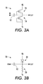
- Circuit 10 comprises an input In , and output Out, a capacitor 12, a first thin-film transistor (TFT) 14, and a second TFT 16, each of the same polarity.
- Circuit 10 of Fig. 3A is intended to model a circuit 18 shown in Fig. 3B , in that TFT 14 models resistor 20 and TFT 16 models diode 22, with operation as follows.
- a rising edge on In of circuit 10 is passed through a high-pass filter made up of capacitor 12 and TFT 14 (e.g., resistor 20) to Out.
- Diode bias V b is set to a voltage such that TFT 16 (e.g., diode 22, Fig. 3B ) prevents Out from being negative.
- Voltage V b is approximately one diode-drop above ground.
- negative voltages may be allowed on signal Out, in which case V b can simply be set to ground.
- Other values of V b may also be acceptable, depending on the application.
- one or both of the TFTs 14, 16 can be replaced by their equivalent components, 20 and 22, respectively, where diodes and resistors are available.
- capacitor 12 can be implemented in the OTF process (for example, with gate dielectric between gate and source/drain metal layer with no semiconductor) or separately.
- Fig. 4 shows a first alternate embodiment of a pulse generator circuit 24 tailored for fabrication by organic thin-film (OTF) processes.
- Circuit 24 comprises an input In , and output Out, a capacitor 26, a first thin-film transistor (TFT) 28 (acting as a resistor), and a second TFT 30, each of the same polarity, similar to the embodiment illustrated and described above with regard to Fig. 3A .
- Circuit 24 further comprises a pass TFT 32 connecting the output of the circuit to a load.
- a rising edge on In generates a pulse at P.
- TFT 30 is sized much wider than TFT 28 to function as a diode.
- the dc value of P is given by V b minus the threshold voltage of TFT 30 (V 30 ), and may be set to ground (but can be other values). In particular, if an additional voltage rail is not available or desired, V b can be tied to ground and P clamped at -V 30 . A low signal on EnBar will pass the pulse P to Out through TFT 32. (The on-characteristic of TFT 32 will further filter the pulse signal.)
- the sizes of TFTs such as 14 and 16, 28 and 30, etc. are determined based on the source impedance seen at In.
- the source impedance Rs is the output impedance of the circuit driving the pulse generator and is not part of the pulse generator circuit itself. At high frequency (s ⁇ ), the transfer function is approximately 1 when R x >> R s and approximately 0 when R x ⁇ R s .
- TFT 30 acts as a diode in the sense that it is off during a positive pulse and on during a negative pulse.
- R on of TFT 28 is much greater than R s
- R on of TFT 30 is much less than R s
- positive pulses will be generated while negative pulses are shunted.
- the on-resistance of TFT 32 is usually non-negligible and will be accounted for in the transfer function analysis.
- the circuit described above may be fabricated on a flexible polyethylene naphthalate substrate by an additive OFT process that includes ink-jet deposition of the metal and semiconductor layers.
- the capacitor may be a parallel plate structure formed by the gate dielectric and the source-drain and gate metals.
- Other substrate materials and structures may be employed depending on the design criteria and application of embodiments of the present disclosure.
- a transmission gate can be used. By placing multiple pass transistors in parallel, the pulse can be selectively connected to one or more of several outputs.
- TFTs 14, 16 of embodiment 10 ( Fig. 3A ) and TFTs 28, 30, 32 of embodiment 24 ( Fig. 4 ) are highly dependent on the application and implementation of the respective circuits, in particular on the characteristics of the TFTs themselves (threshold voltage, mobility, etc.), the process design rules (minimum channel length, available channel widths), and the load resistance and capacitance. Additionally, they are dependent on the desired pulse duration and shape.
- Fig. 5 shows In , EnBar, P, and Out values plotted against time in a simulation of circuit 24 ( Fig. 4 ) for a printed OTF process.
- V b 0 volts
- a capacitance of capacitor 26 was 200 pF.
- Each of TFTs 28, 30, and 32 had a channel length of 35 ⁇ m.
- the channel widths of TFTs 28, 30 and 32 were 200 ⁇ m, 6 mm, and 400 ⁇ m, respectively.
- the length and width are process dependent. According to one embodiment, length may range from 2 ⁇ m to 200 ⁇ m, and widths may range from 100 ⁇ m to 1 cm. It will be noted that a rising pulse on In (at approximately 58 ms) triggers a pulse on Out when EnBar is low.
- Fig. 6 shows measured output of circuit 24 ( Fig. 4 ).
- TFTs 28, 30, and 32 had a approximate channel length of 35 ⁇ m.
- the channel widths of TFTs 28, 30 and 32 were approximately 200 ⁇ m, 6 mm, and 400 ⁇ m, respectively..
- the voltage V b was 3.5 volts.
- Capacitor 26 had a value of 200 pF. Again, it will be noted that a rising pulse on In (at 40 ms) triggers an output pulse.
- Figs. 7 through 11 Illustrated in Figs. 7 through 11 are various alternate embodiments of a pulse generator circuit tailored for fabrication by OTF processes. More specifically, Fig. 7 includes TFTs 42, 44, and 46 similar to those described with reference to Fig. 4 . In addition, the circuit of Fig. 7 includes an additional enable TFT 48, enabled when a voltage En is high. In typical operation, signal En is the complement of EnBar at all times. When En is low (disabled), TFT 48 serves to aid in clamping Out near ground.
- Fig. 8 is an alternate embodiment for filtering the pulse on Out in which TFT 42 from Fig. 7 has been eliminated, leaving TFTs 52, 54, and 56. In function, TFT 56 serves in place of TFT 28 of Fig. 4 .
- Ena at the gate of TFT 56 is an analog voltage that sets the effective resistance of TFT 56.
- Fig. 9 is a modification of the circuit of Fig. 4 including TFTs 62, 64, 66, in which TFT 62 corresponding to the resistor (20 of Fig. 3B ) has been relocated to the output side of TFT 66.
- Fig. 10 is an illustration of a N-channel TFT implementation of the circuit illustrated in Fig. 3A , including N-channel TFTs 72, 74.
- Fig. 11 is an illustration of a N-channel TFT implementation of the circuit illustrated in Fig. 4 , including N-channel TFTs 82, 84, 86.
Landscapes
- Physics & Mathematics (AREA)
- Nonlinear Science (AREA)
- Thin Film Transistor (AREA)
- Metal-Oxide And Bipolar Metal-Oxide Semiconductor Integrated Circuits (AREA)
Abstract
Description
- The present disclosure is related to digital electronic circuits, and more specifically to a pulse generator circuit optimized for printed, solution processed thin-film devices.
- A pulse generator, also called a monostable multivibrator or one-shot, is a common element of many circuits in a wide range of applications. One common use is for switch debouncing. Another is as a reset signal generator. The input to a one-shot is an edge or pulse and the output is a positive or negative voltage pulse. The duration and magnitude of the pulse can be fixed or settable and are generally constrained to fall within ranges specified for the application.
Fig. 1 shows a timing diagram of an example of a one-shot circuit. - A common circuit implementation of a monostable multivibrator includes an inverter and a NAND or NOR gate.
Fig. 2 is an example of such an implementation. This circuit is a rising-edge-triggered negative pulse generator. In this circuit, input signal In is normally low, and inverter output D is high, making output signal Out high. When a rising edge is sent to In, output Out switches to low until the edge propagates through the inverter to D. Once D switches to low, Out returns to the high state. The duration of the pulse is determined by the propagation delay through the inverter. This can be controlled by the sizes of the transistors making up the inverter and NAND gate and/or by including additional delay elements, such as additional inverters or capacitors, to the D signal. Of course, many other implementations are known in the art. - There is a desire to produce devices such as the aforementioned monostable multivibrator using printed thin-film processes such as, but not limited to, those employing organic thin film (OTF) material systems. OTF fabrication processes are much less mature than crystalline silicon technologies, and direct implementation of conventional complementary designs is challenging due to the relatively low yield, high variability, and instability of devices formed by printed OTF processes. For example, in certain of such process reliable fabrication of all integrated devices in a single process is problematic. Further, according to some OTF processes, only one or the other of N- and P-channel devices may be formed (not both simultaneously). In processes capable of producing both N- and P-channel devices, one device type often has significantly higher performance than the other. And, process-based limits on device size in combination with large parasitic capacitances limit design of devices having desired pulse widths.
- In light of these limitations, there is a need in the art for a device design capable of use within the context of OTF processes, such as circuit designs that include a minimum number of thin-film transistors (TFTs) and a single polarity. Such are disclosed herein.
- Accordingly, the present disclosure is directed to circuit designs for converting an edge output by a sensor to a signal that addresses the difficulties of forming such circuits using solution-based and printed processes. The circuits provide a pulse sustained above a voltage threshold for a minimum time interval. Applications include clocking flip-flops, generating reset signals, polarizing a memory cell, and so on. The devices may be fabricated in an all-additive inkjet process. For the clarity and simplicity, processing using organic material (organic thin-film, OTF) is referred to below as an example of solution-based printed process, although it will be appreciated that many different types of solutions and materials, whether organic or inorganic, are contemplated herein and within the scope of the present disclosure. Therefore, OTF and organic material will be understood to be examples only, and the scope of the disclosure not limited thereby.
- According to one aspect of the disclosure, an electronic pulse-generator circuit comprises: an input node; a capacitor communicatively connected at to the input node and to a pulse line; a first thin film transistor having a channel formed of a first polarity organic semiconductor material, a first side of the channel communicatively connected to a first voltage source, a second side of the channel communicatively connected to the pulse line, the first thin film transistor configured to function as a diode; a second thin film transistor having a channel formed of the first polarity organic semiconductor material, a first side of the channel communicatively connected to the pulse line, a second side of the channel communicatively connected to a second voltage source (e.g., ground), the second thin film transistor configured to function as a resistor; and an output node communicatively connected to receive a pulse from the pulse line.
- Implementations of this aspect may also include a third thin film transistor having a channel formed of the first polarity organic semiconductor material, a first side of said channel communicatively connected to the pulse line, a second side of the channel communicatively connected to the output node, and further comprising a gate communicatively connected to a first enable signal line.
- According to another aspect of the disclosure, the first polarity organic semiconductor material is p-type.
- Implementations may also include the first thin film transistor further comprising a gate communicatively connected to the pulse line at the capacitor, and further wherein the second thin film transistor further comprises a gate communicatively connected to the second voltage source (e.g., ground).
- Other implementations of the present disclosure are also provided and discussed in greater detail, below. Thus, the above is merely a brief summary of a number of unique aspects, features, and advantages of the present disclosure. The above summary is not intended to be nor should it be read as an exclusive identification of aspects, features, or advantages of the claimed subject matter. Therefore, the above summary should not be read as imparting limitations to the claims nor in any other way determining the scope of said claims.
- It should be noted that the present disclosure focuses on solution-proceed devices. These are devices having one or more layers formed from the deposition of materials solution phase, which solidify (such as by evaporation). One form of solution processing is printing of patterned solution. Materials capable of solution processing may be either organic or inorganic. While this disclosure uses printed organic semiconductor technologies as an example, the invention is equally applicable to other process technologies. Furthermore, the invention can be implemented in other TFT technologies that are not solution based. Therefore, in this disclosure, references to solution processing, printing, and organic materials should be read as examples, not limiting distinctions.
- In the drawings appended hereto like reference numerals denote like elements between the various drawings. While illustrative, the drawings are not drawn to scale. In the drawings:
-
Fig. 1 is a timing diagram of a positive-edge-triggered one-shot circuit with pulse duration, d, and voltage amplitude, v, as known in the art. -
Fig. 2 is an implementation of a monostable multivibrator including an inverter and a NAND or NOR gate as known in the art. -
Fig. 3A is a schematic illustration of one embodiment of a pulse generator circuit, tailored for fabrication by organic thin-film processes, according to the present disclosure. -
Fig. 3B is a schematic illustration of an equivalent circuit to that shown inFig. 3A of an embodiment of a pulse generator circuit, tailored for fabrication by organic thin-film processes, according to the present disclosure. -
Fig. 4 is a schematic illustration of an alternate embodiment of a pulse generator circuit, tailored for fabrication by organic thin-film processes, according to the present disclosure. -
Fig. 5 is a plot of a simulation illustrating various voltages on lines as a function of time for the embodiment shown inFig. 4 . -
Fig. 6 is a plot of In and Out voltages for an actual example of the circuit ofFig. 4 plotted against time. -
Fig. 7 is a schematic illustration of another alternate embodiment of a pulse generator circuit, tailored for fabrication by organic thin-film processes, according to the present disclosure. -
Fig. 8 is a schematic illustration of yet another alternate embodiment of a pulse generator circuit, tailored for fabrication by organic thin-film processes, according to the present disclosure. -
Fig. 9 is a schematic illustration of still another alternate embodiment of a pulse generator circuit, tailored for fabrication by organic thin-film processes, according to the present disclosure. -
Fig. 10 is a schematic illustration of a still further alternate embodiment of a pulse generator circuit, tailored for fabrication by organic thin-film processes, according to the present disclosure. -
Fig. 11 is a schematic illustration of an additional alternate embodiment of a pulse generator circuit, tailored for fabrication by organic thin-film processes, according to the present disclosure. - We initially point out that description of well-known starting materials, processing techniques, components, equipment and other well-known details may merely be summarized or are omitted so as not to unnecessarily obscure the details of the present disclosure. Thus, where details are otherwise well-known, we leave it to the application of the present disclosure to suggest or dictate choices relating to those details.
- With reference to
Fig. 3A , there is shown therein a first embodiment of apulse generator circuit 10 tailored for fabrication by organic thin-film (OTF) processes.Circuit 10 comprises an input In, and output Out, acapacitor 12, a first thin-film transistor (TFT) 14, and asecond TFT 16, each of the same polarity.Circuit 10 ofFig. 3A is intended to model acircuit 18 shown inFig. 3B , in thatTFT 14models resistor 20 andTFT 16models diode 22, with operation as follows. A rising edge on In ofcircuit 10 is passed through a high-pass filter made up ofcapacitor 12 and TFT 14 (e.g., resistor 20) to Out. Diode bias Vb is set to a voltage such that TFT 16 (e.g.,diode 22,Fig. 3B ) prevents Out from being negative. Voltage Vb is approximately one diode-drop above ground. Depending on the implementation, negative voltages may be allowed on signal Out, in which case Vb can simply be set to ground. Other values of Vb may also be acceptable, depending on the application. In some implementations, one or both of theTFTs capacitor 12 can be implemented in the OTF process (for example, with gate dielectric between gate and source/drain metal layer with no semiconductor) or separately. -
Fig. 4 shows a first alternate embodiment of apulse generator circuit 24 tailored for fabrication by organic thin-film (OTF) processes.Circuit 24 comprises an input In, and output Out, acapacitor 26, a first thin-film transistor (TFT) 28 (acting as a resistor), and asecond TFT 30, each of the same polarity, similar to the embodiment illustrated and described above with regard toFig. 3A .Circuit 24 further comprises apass TFT 32 connecting the output of the circuit to a load. A rising edge on In generates a pulse at P. The generation of a complimentary negative pulse with a falling edge is prevented byTFT 30, which is sized much wider thanTFT 28 to function as a diode. The dc value of P is given by Vb minus the threshold voltage of TFT 30 (V30), and may be set to ground (but can be other values). In particular, if an additional voltage rail is not available or desired, Vb can be tied to ground and P clamped at -V30. A low signal on EnBar will pass the pulse P to Out throughTFT 32. (The on-characteristic ofTFT 32 will further filter the pulse signal.) - In principal, the sizes of TFTs such as 14 and 16, 28 and 30, etc. are determined based on the source impedance seen at In. The transfer function from the source to P is given by

where Rx is the channel resistance ofTFT 28 for a positive pulse and ofTFT 30 for a negative pulse, Rs is the source impedance, C is the capacitance ofcapacitor 26, and s is the Laplace parameter. The source impedance Rs is the output impedance of the circuit driving the pulse generator and is not part of the pulse generator circuit itself. At high frequency (s →∞), the transfer function is approximately 1 when Rx >> Rs and approximately 0 when Rx << Rs. TFT 30 acts as a diode in the sense that it is off during a positive pulse and on during a negative pulse. Thus, if Ron ofTFT 28 is much greater than Rs, and Ron ofTFT 30 is much less than Rs, positive pulses will be generated while negative pulses are shunted. In practice, the on-resistance ofTFT 32 is usually non-negligible and will be accounted for in the transfer function analysis. - The circuit described above may be fabricated on a flexible polyethylene naphthalate substrate by an additive OFT process that includes ink-jet deposition of the metal and semiconductor layers. The capacitor may be a parallel plate structure formed by the gate dielectric and the source-drain and gate metals. Other substrate materials and structures may be employed depending on the design criteria and application of embodiments of the present disclosure.
- Alternatively, if both n- and p-channel devices are available, a transmission gate can be used. By placing multiple pass transistors in parallel, the pulse can be selectively connected to one or more of several outputs.
- The sizes of
TFTs Fig. 3A ) andTFTs Fig. 4 ) are highly dependent on the application and implementation of the respective circuits, in particular on the characteristics of the TFTs themselves (threshold voltage, mobility, etc.), the process design rules (minimum channel length, available channel widths), and the load resistance and capacitance. Additionally, they are dependent on the desired pulse duration and shape. -
Fig. 5 shows In, EnBar, P, and Out values plotted against time in a simulation of circuit 24 (Fig. 4 ) for a printed OTF process. In this simulation, a 20-volt input step, Vb = 0 volts, and a 10 pF capacitive load were used. A capacitance ofcapacitor 26 was 200 pF. Each ofTFTs TFTs -
Fig. 6 shows measured output of circuit 24 (Fig. 4 ). Each ofTFTs TFTs Capacitor 26 had a value of 200 pF. Again, it will be noted that a rising pulse on In (at 40 ms) triggers an output pulse. - Illustrated in
Figs. 7 through 11 are various alternate embodiments of a pulse generator circuit tailored for fabrication by OTF processes. More specifically,Fig. 7 includesTFTs Fig. 4 . In addition, the circuit ofFig. 7 includes anadditional enable TFT 48, enabled when a voltage En is high. In typical operation, signal En is the complement of EnBar at all times. When En is low (disabled),TFT 48 serves to aid in clamping Out near ground.Fig. 8 is an alternate embodiment for filtering the pulse on Out in whichTFT 42 fromFig. 7 has been eliminated, leavingTFTs TFT 56 serves in place ofTFT 28 ofFig. 4 . Here, Ena at the gate ofTFT 56 is an analog voltage that sets the effective resistance ofTFT 56.Fig. 9 is a modification of the circuit ofFig. 4 includingTFTs TFT 62 corresponding to the resistor (20 ofFig. 3B ) has been relocated to the output side ofTFT 66. -
Fig. 10 is an illustration of a N-channel TFT implementation of the circuit illustrated inFig. 3A , including N-channel TFTs Fig. 11 is an illustration of a N-channel TFT implementation of the circuit illustrated inFig. 4 , including N-channel TFTs - The physics of modern electrical devices and the methods of their production are not absolutes, but rather statistical efforts to produce a desired device and/or result. Even with the utmost of attention being paid to repeatability of processes, the cleanliness of manufacturing facilities, the purity of starting and processing materials, and so forth, variations and imperfections result. Accordingly, no limitation in the description of the present disclosure or its claims can or should be read as absolute. The limitations of the claims are intended to define the boundaries of the present disclosure, up to and including those limitations. To further highlight this, the term "substantially" may occasionally be used herein in association with a claim limitation (although consideration for variations and imperfections is not restricted to only those limitations used with that term). While as difficult to precisely define as the limitations of the present disclosure themselves, we intend that this term be interpreted as "to a large extent", "as nearly as practicable", "within technical limitations", and the like.
- While examples and variations have been presented in the foregoing description, it should be understood that a vast number of variations exist, and these examples are merely representative, and are not intended to limit the scope, applicability or configuration of the disclosure in any way. Various of the above-disclosed and other features and functions, or alternative thereof, may be desirably combined into many other different systems or applications. Various presently unforeseen or unanticipated alternatives, modifications variations, or improvements therein or thereon may be subsequently made by those skilled in the art which are also intended to be encompassed by the claims, below.
- Therefore, the foregoing description provides those of ordinary skill in the art with a convenient guide for implementation of the disclosure, and contemplates that various changes in the functions and arrangements of the described examples may be made without departing from the scope of the disclosure defined by the claims thereto. It will be understood that features disclosed in association with a particular embodiment are intended to be interchangeable with other embodiments unless the context would prevent it.
Claims (12)
- An electronic pulse-generator circuit, comprising:an input node;a capacitor communicatively connected to said input node and to a pulse line;a first thin film transistor having a channel formed of a first polarity solution-processed semiconductor material, a first side of said channel communicatively connected to a first voltage source, a second side of said channel communicatively connected to said pulse line, said first thin film transistor configured to function as a diode;a second thin film transistor having a channel formed of said first polarity solution-processed semiconductor material, a first side of said channel communicatively connected to said pulse line, a second side of said channel communicatively connected to a second voltage source, said second thin film transistor configured to function as a resistor; andan output node communicatively connected to receive a pulse from said pulse line.
- The electronic pulse-generator circuit of claim 1 wherein said first polarity solution-processed semiconductor material is P-type.
- The electronic pulse-generator circuit of claim 1 or claim 2, further comprising a third thin film transistor having a channel formed of said first polarity solution-processed semiconductor material, a first side of said channel communicatively connected to said pulse line, a second side of said channel communicatively connected to said output node, and further comprising a gate communicatively connected to a first enable signal line.
- The electronic pulse-generator circuit of claim 3, further comprising a fourth thin film transistor having a channel formed of said first polarity solution-processed semiconductor material, a first side of said channel communicatively connected to said pulse line at said output node, a second side of said channel communicatively connected to a third voltage source, and further comprising a gate communicatively connected to a second enable signal line.
- The electronic pulse-generator circuit of claim 3 or claim 4, wherein said first side of said channel of said second thin film transistor is communicatively connected to said pulse line at said output node.
- The electronic pulse-generator circuit of claim 5, wherein said second thin film transistor further comprises a gate communicatively connected to a third enable signal line.
- The electronic pulse-generator circuit of any of claims 3 to 6, wherein said second voltage source is ground.
- The electronic pulse-generator circuit of claim 1, wherein said first polarity solution-processed semiconductor material is N-type.
- The electronic pulse-generator circuit of claim 8, wherein said first thin film transistor comprises a gate communicatively connected to said first voltage source, and further wherein said second thin film transistor further comprises a gate communicatively connected to said pulse line, said capacitor, and said second side of said channel of said first thin film transistor.
- The electronic pulse-generator circuit of claim 1, wherein said first thin film transistor further comprises a gate communicatively connected to said pulse line, said capacitor, and said second side of said channel of said first thin film transistor, and further wherein said second thin film transistor further comprises a gate communicatively connected to ground.
- The electronic pulse-generator circuit of claim 1, wherein said first polarity solution-processed semiconductor material is N-type.
- The electronic pulse-generator circuit of claim 11, wherein said first thin film transistor comprises a gate communicatively connected to said voltage source, and further wherein said second thin film transistor further comprises a gate communicatively connected to said pulse line, said capacitor, and said second side of said channel of said first thin film transistor.
Applications Claiming Priority (1)
| Application Number | Priority Date | Filing Date | Title |
|---|---|---|---|
| US13/715,675 US8723578B1 (en) | 2012-12-14 | 2012-12-14 | Pulse generator circuit |
Publications (2)
| Publication Number | Publication Date |
|---|---|
| EP2744109A1 true EP2744109A1 (en) | 2014-06-18 |
| EP2744109B1 EP2744109B1 (en) | 2016-05-11 |
Family
ID=49999662
Family Applications (1)
| Application Number | Title | Priority Date | Filing Date |
|---|---|---|---|
| EP13197356.2A Not-in-force EP2744109B1 (en) | 2012-12-14 | 2013-12-16 | Pulse generator circuit |
Country Status (2)
| Country | Link |
|---|---|
| US (2) | US8723578B1 (en) |
| EP (1) | EP2744109B1 (en) |
Families Citing this family (2)
| Publication number | Priority date | Publication date | Assignee | Title |
|---|---|---|---|---|
| US8723578B1 (en) | 2012-12-14 | 2014-05-13 | Palo Alto Research Center Incorporated | Pulse generator circuit |
| CN105337590B (en) * | 2015-10-26 | 2017-10-17 | 宁波大学 | It is a kind of bilateral along pulse signal generator based on CNFET |
Citations (6)
| Publication number | Priority date | Publication date | Assignee | Title |
|---|---|---|---|---|
| US3508084A (en) * | 1967-10-06 | 1970-04-21 | Texas Instruments Inc | Enhancement-mode mos circuitry |
| JPS59103421A (en) * | 1982-12-06 | 1984-06-14 | Matsushita Electric Ind Co Ltd | pulse delay circuit |
| US5925905A (en) * | 1995-01-24 | 1999-07-20 | Siemens Aktiengesellschaft | MOS circuit configuration for switching high voltages on a semiconductor chip |
| JP2000196023A (en) * | 1998-10-20 | 2000-07-14 | Hitachi Ltd | Boost circuit device and semiconductor integrated circuit device using the same |
| US6433623B1 (en) * | 1998-10-20 | 2002-08-13 | Hitachi, Ltd. | Voltage booster circuit control method |
| US20040041614A1 (en) * | 2002-02-26 | 2004-03-04 | Youichi Tobita | Amplitude converting circuit |
Family Cites Families (8)
| Publication number | Priority date | Publication date | Assignee | Title |
|---|---|---|---|---|
| JPS5593252A (en) * | 1979-01-05 | 1980-07-15 | Mitsubishi Electric Corp | Substrate potential generating apparatus |
| JPS5632758A (en) * | 1979-08-27 | 1981-04-02 | Fujitsu Ltd | Substrate bias generating circuit |
| JP2001036388A (en) * | 1999-07-16 | 2001-02-09 | Sharp Corp | Level shift circuit and semiconductor device |
| US6472918B1 (en) * | 1999-08-23 | 2002-10-29 | Level One Communications, Inc. | Self-referencing slicer method and apparatus for high-accuracy clock duty cycle generation |
| US7288980B2 (en) * | 2002-11-05 | 2007-10-30 | Ip-First, Llc | Multiple mode clock receiver |
| CN101442298A (en) * | 2007-11-20 | 2009-05-27 | 深圳富泰宏精密工业有限公司 | Pulse generation apparatus |
| US8053753B2 (en) * | 2008-06-06 | 2011-11-08 | Ovonyx, Inc. | Thin film logic circuitry |
| US8723578B1 (en) | 2012-12-14 | 2014-05-13 | Palo Alto Research Center Incorporated | Pulse generator circuit |
-
2012
- 2012-12-14 US US13/715,675 patent/US8723578B1/en active Active
-
2013
- 2013-12-16 EP EP13197356.2A patent/EP2744109B1/en not_active Not-in-force
-
2014
- 2014-05-13 US US14/276,488 patent/US9172357B2/en not_active Expired - Fee Related
Patent Citations (6)
| Publication number | Priority date | Publication date | Assignee | Title |
|---|---|---|---|---|
| US3508084A (en) * | 1967-10-06 | 1970-04-21 | Texas Instruments Inc | Enhancement-mode mos circuitry |
| JPS59103421A (en) * | 1982-12-06 | 1984-06-14 | Matsushita Electric Ind Co Ltd | pulse delay circuit |
| US5925905A (en) * | 1995-01-24 | 1999-07-20 | Siemens Aktiengesellschaft | MOS circuit configuration for switching high voltages on a semiconductor chip |
| JP2000196023A (en) * | 1998-10-20 | 2000-07-14 | Hitachi Ltd | Boost circuit device and semiconductor integrated circuit device using the same |
| US6433623B1 (en) * | 1998-10-20 | 2002-08-13 | Hitachi, Ltd. | Voltage booster circuit control method |
| US20040041614A1 (en) * | 2002-02-26 | 2004-03-04 | Youichi Tobita | Amplitude converting circuit |
Also Published As
| Publication number | Publication date |
|---|---|
| EP2744109B1 (en) | 2016-05-11 |
| US8723578B1 (en) | 2014-05-13 |
| US20140247079A1 (en) | 2014-09-04 |
| US9172357B2 (en) | 2015-10-27 |
Similar Documents
| Publication | Publication Date | Title |
|---|---|---|
| US8797071B2 (en) | Semiconductor device including power-on reset circuit | |
| US8369054B2 (en) | NMOS-based feedback power-clamp for on-chip ESD protection | |
| US9640988B2 (en) | Comparative ESD power clamp | |
| EP3357090B1 (en) | Electrostatic discharge protection device and circuit apparatus | |
| KR101293845B1 (en) | Delay circuit | |
| JP6440224B2 (en) | Row drive circuit for oxide semiconductor thin film transistor | |
| EP2547096A2 (en) | Solid-state image sensing apparatus | |
| US20150249334A1 (en) | Electrostatic discharge circuit with reduced standby current | |
| CN1979816B (en) | Diode circuit and clamp circuit, diode manufacture method and pressure limiting method | |
| EP2541769B1 (en) | Oscillator circuit and electronic system comprising oscillator circuit | |
| EP2744109B1 (en) | Pulse generator circuit | |
| CN105528977A (en) | Detection circuit, drive integrated circuit and detection method thereof | |
| US8873270B2 (en) | Pulse generator and ferroelectric memory circuit | |
| KR20160038828A (en) | Oscillator circuit | |
| US11519786B2 (en) | Temperature detection circuit, temperature sensor device and display device | |
| CN101807436B (en) | shift register | |
| EP2963820B1 (en) | High voltage driver | |
| JP6352042B2 (en) | Delay circuit, oscillation circuit, and semiconductor device | |
| CN109245507B (en) | Overshoot-preventing protection circuit | |
| Liao et al. | P‐28: Robust Gate Driver Design with Etching‐Stop‐Layer Type InGaZnO TFTs Using Stack Buffer Structure | |
| US5982247A (en) | CR oscillating circuit | |
| EP2731267B1 (en) | Interleaved transient filter and method | |
| US8884689B2 (en) | Low pass filter with an increased delay | |
| US10084432B1 (en) | Semiconductor device | |
| RU2661282C1 (en) | Device for the semiconductor micro-assemblies protection against the thyristor effect |
Legal Events
| Date | Code | Title | Description |
|---|---|---|---|
| PUAI | Public reference made under article 153(3) epc to a published international application that has entered the european phase |
Free format text: ORIGINAL CODE: 0009012 |
|
| 17P | Request for examination filed |
Effective date: 20131216 |
|
| AK | Designated contracting states |
Kind code of ref document: A1 Designated state(s): AL AT BE BG CH CY CZ DE DK EE ES FI FR GB GR HR HU IE IS IT LI LT LU LV MC MK MT NL NO PL PT RO RS SE SI SK SM TR |
|
| AX | Request for extension of the european patent |
Extension state: BA ME |
|
| R17P | Request for examination filed (corrected) |
Effective date: 20141114 |
|
| RBV | Designated contracting states (corrected) |
Designated state(s): AL AT BE BG CH CY CZ DE DK EE ES FI FR GB GR HR HU IE IS IT LI LT LU LV MC MK MT NL NO PL PT RO RS SE SI SK SM TR |
|
| 17Q | First examination report despatched |
Effective date: 20150202 |
|
| REG | Reference to a national code |
Ref country code: DE Ref legal event code: R079 Ref document number: 602013007406 Country of ref document: DE Free format text: PREVIOUS MAIN CLASS: H03K0003355000 Ipc: H03K0003012000 |
|
| GRAP | Despatch of communication of intention to grant a patent |
Free format text: ORIGINAL CODE: EPIDOSNIGR1 |
|
| RIC1 | Information provided on ipc code assigned before grant |
Ipc: H03K 3/355 20060101ALI20151130BHEP Ipc: H03K 3/012 20060101AFI20151130BHEP Ipc: H03K 5/04 20060101ALI20151130BHEP |
|
| INTG | Intention to grant announced |
Effective date: 20160104 |
|
| GRAS | Grant fee paid |
Free format text: ORIGINAL CODE: EPIDOSNIGR3 |
|
| GRAA | (expected) grant |
Free format text: ORIGINAL CODE: 0009210 |
|
| AK | Designated contracting states |
Kind code of ref document: B1 Designated state(s): AL AT BE BG CH CY CZ DE DK EE ES FI FR GB GR HR HU IE IS IT LI LT LU LV MC MK MT NL NO PL PT RO RS SE SI SK SM TR |
|
| REG | Reference to a national code |
Ref country code: GB Ref legal event code: FG4D |
|
| REG | Reference to a national code |
Ref country code: CH Ref legal event code: EP |
|
| REG | Reference to a national code |
Ref country code: AT Ref legal event code: REF Ref document number: 799367 Country of ref document: AT Kind code of ref document: T Effective date: 20160515 |
|
| REG | Reference to a national code |
Ref country code: IE Ref legal event code: FG4D |
|
| REG | Reference to a national code |
Ref country code: DE Ref legal event code: R096 Ref document number: 602013007406 Country of ref document: DE |
|
| REG | Reference to a national code |
Ref country code: LT Ref legal event code: MG4D |
|
| REG | Reference to a national code |
Ref country code: NL Ref legal event code: MP Effective date: 20160511 |
|
| PG25 | Lapsed in a contracting state [announced via postgrant information from national office to epo] |
Ref country code: NL Free format text: LAPSE BECAUSE OF FAILURE TO SUBMIT A TRANSLATION OF THE DESCRIPTION OR TO PAY THE FEE WITHIN THE PRESCRIBED TIME-LIMIT Effective date: 20160511 Ref country code: NO Free format text: LAPSE BECAUSE OF FAILURE TO SUBMIT A TRANSLATION OF THE DESCRIPTION OR TO PAY THE FEE WITHIN THE PRESCRIBED TIME-LIMIT Effective date: 20160811 Ref country code: FI Free format text: LAPSE BECAUSE OF FAILURE TO SUBMIT A TRANSLATION OF THE DESCRIPTION OR TO PAY THE FEE WITHIN THE PRESCRIBED TIME-LIMIT Effective date: 20160511 Ref country code: LT Free format text: LAPSE BECAUSE OF FAILURE TO SUBMIT A TRANSLATION OF THE DESCRIPTION OR TO PAY THE FEE WITHIN THE PRESCRIBED TIME-LIMIT Effective date: 20160511 |
|
| REG | Reference to a national code |
Ref country code: AT Ref legal event code: MK05 Ref document number: 799367 Country of ref document: AT Kind code of ref document: T Effective date: 20160511 |
|
| REG | Reference to a national code |
Ref country code: FR Ref legal event code: PLFP Year of fee payment: 4 |
|
| PG25 | Lapsed in a contracting state [announced via postgrant information from national office to epo] |
Ref country code: LV Free format text: LAPSE BECAUSE OF FAILURE TO SUBMIT A TRANSLATION OF THE DESCRIPTION OR TO PAY THE FEE WITHIN THE PRESCRIBED TIME-LIMIT Effective date: 20160511 Ref country code: GR Free format text: LAPSE BECAUSE OF FAILURE TO SUBMIT A TRANSLATION OF THE DESCRIPTION OR TO PAY THE FEE WITHIN THE PRESCRIBED TIME-LIMIT Effective date: 20160812 Ref country code: PT Free format text: LAPSE BECAUSE OF FAILURE TO SUBMIT A TRANSLATION OF THE DESCRIPTION OR TO PAY THE FEE WITHIN THE PRESCRIBED TIME-LIMIT Effective date: 20160912 Ref country code: HR Free format text: LAPSE BECAUSE OF FAILURE TO SUBMIT A TRANSLATION OF THE DESCRIPTION OR TO PAY THE FEE WITHIN THE PRESCRIBED TIME-LIMIT Effective date: 20160511 Ref country code: RS Free format text: LAPSE BECAUSE OF FAILURE TO SUBMIT A TRANSLATION OF THE DESCRIPTION OR TO PAY THE FEE WITHIN THE PRESCRIBED TIME-LIMIT Effective date: 20160511 Ref country code: ES Free format text: LAPSE BECAUSE OF FAILURE TO SUBMIT A TRANSLATION OF THE DESCRIPTION OR TO PAY THE FEE WITHIN THE PRESCRIBED TIME-LIMIT Effective date: 20160511 Ref country code: SE Free format text: LAPSE BECAUSE OF FAILURE TO SUBMIT A TRANSLATION OF THE DESCRIPTION OR TO PAY THE FEE WITHIN THE PRESCRIBED TIME-LIMIT Effective date: 20160511 |
|
| PG25 | Lapsed in a contracting state [announced via postgrant information from national office to epo] |
Ref country code: IT Free format text: LAPSE BECAUSE OF FAILURE TO SUBMIT A TRANSLATION OF THE DESCRIPTION OR TO PAY THE FEE WITHIN THE PRESCRIBED TIME-LIMIT Effective date: 20160511 |
|
| PG25 | Lapsed in a contracting state [announced via postgrant information from national office to epo] |
Ref country code: RO Free format text: LAPSE BECAUSE OF FAILURE TO SUBMIT A TRANSLATION OF THE DESCRIPTION OR TO PAY THE FEE WITHIN THE PRESCRIBED TIME-LIMIT Effective date: 20160511 Ref country code: CZ Free format text: LAPSE BECAUSE OF FAILURE TO SUBMIT A TRANSLATION OF THE DESCRIPTION OR TO PAY THE FEE WITHIN THE PRESCRIBED TIME-LIMIT Effective date: 20160511 Ref country code: SK Free format text: LAPSE BECAUSE OF FAILURE TO SUBMIT A TRANSLATION OF THE DESCRIPTION OR TO PAY THE FEE WITHIN THE PRESCRIBED TIME-LIMIT Effective date: 20160511 Ref country code: EE Free format text: LAPSE BECAUSE OF FAILURE TO SUBMIT A TRANSLATION OF THE DESCRIPTION OR TO PAY THE FEE WITHIN THE PRESCRIBED TIME-LIMIT Effective date: 20160511 Ref country code: DK Free format text: LAPSE BECAUSE OF FAILURE TO SUBMIT A TRANSLATION OF THE DESCRIPTION OR TO PAY THE FEE WITHIN THE PRESCRIBED TIME-LIMIT Effective date: 20160511 |
|
| REG | Reference to a national code |
Ref country code: DE Ref legal event code: R097 Ref document number: 602013007406 Country of ref document: DE |
|
| PG25 | Lapsed in a contracting state [announced via postgrant information from national office to epo] |
Ref country code: SM Free format text: LAPSE BECAUSE OF FAILURE TO SUBMIT A TRANSLATION OF THE DESCRIPTION OR TO PAY THE FEE WITHIN THE PRESCRIBED TIME-LIMIT Effective date: 20160511 Ref country code: PL Free format text: LAPSE BECAUSE OF FAILURE TO SUBMIT A TRANSLATION OF THE DESCRIPTION OR TO PAY THE FEE WITHIN THE PRESCRIBED TIME-LIMIT Effective date: 20160511 Ref country code: BE Free format text: LAPSE BECAUSE OF FAILURE TO SUBMIT A TRANSLATION OF THE DESCRIPTION OR TO PAY THE FEE WITHIN THE PRESCRIBED TIME-LIMIT Effective date: 20160511 Ref country code: AT Free format text: LAPSE BECAUSE OF FAILURE TO SUBMIT A TRANSLATION OF THE DESCRIPTION OR TO PAY THE FEE WITHIN THE PRESCRIBED TIME-LIMIT Effective date: 20160511 |
|
| PLBE | No opposition filed within time limit |
Free format text: ORIGINAL CODE: 0009261 |
|
| STAA | Information on the status of an ep patent application or granted ep patent |
Free format text: STATUS: NO OPPOSITION FILED WITHIN TIME LIMIT |
|
| 26N | No opposition filed |
Effective date: 20170214 |
|
| PG25 | Lapsed in a contracting state [announced via postgrant information from national office to epo] |
Ref country code: SI Free format text: LAPSE BECAUSE OF FAILURE TO SUBMIT A TRANSLATION OF THE DESCRIPTION OR TO PAY THE FEE WITHIN THE PRESCRIBED TIME-LIMIT Effective date: 20160511 |
|
| PG25 | Lapsed in a contracting state [announced via postgrant information from national office to epo] |
Ref country code: MC Free format text: LAPSE BECAUSE OF FAILURE TO SUBMIT A TRANSLATION OF THE DESCRIPTION OR TO PAY THE FEE WITHIN THE PRESCRIBED TIME-LIMIT Effective date: 20160511 |
|
| REG | Reference to a national code |
Ref country code: CH Ref legal event code: PL |
|
| REG | Reference to a national code |
Ref country code: IE Ref legal event code: MM4A |
|
| PG25 | Lapsed in a contracting state [announced via postgrant information from national office to epo] |
Ref country code: LU Free format text: LAPSE BECAUSE OF NON-PAYMENT OF DUE FEES Effective date: 20161216 Ref country code: LI Free format text: LAPSE BECAUSE OF NON-PAYMENT OF DUE FEES Effective date: 20161231 Ref country code: CH Free format text: LAPSE BECAUSE OF NON-PAYMENT OF DUE FEES Effective date: 20161231 |
|
| REG | Reference to a national code |
Ref country code: FR Ref legal event code: PLFP Year of fee payment: 5 |
|
| PG25 | Lapsed in a contracting state [announced via postgrant information from national office to epo] |
Ref country code: IE Free format text: LAPSE BECAUSE OF NON-PAYMENT OF DUE FEES Effective date: 20161216 |
|
| PG25 | Lapsed in a contracting state [announced via postgrant information from national office to epo] |
Ref country code: HU Free format text: LAPSE BECAUSE OF FAILURE TO SUBMIT A TRANSLATION OF THE DESCRIPTION OR TO PAY THE FEE WITHIN THE PRESCRIBED TIME-LIMIT; INVALID AB INITIO Effective date: 20131216 |
|
| PG25 | Lapsed in a contracting state [announced via postgrant information from national office to epo] |
Ref country code: CY Free format text: LAPSE BECAUSE OF FAILURE TO SUBMIT A TRANSLATION OF THE DESCRIPTION OR TO PAY THE FEE WITHIN THE PRESCRIBED TIME-LIMIT Effective date: 20160511 Ref country code: MK Free format text: LAPSE BECAUSE OF FAILURE TO SUBMIT A TRANSLATION OF THE DESCRIPTION OR TO PAY THE FEE WITHIN THE PRESCRIBED TIME-LIMIT Effective date: 20160511 Ref country code: IS Free format text: LAPSE BECAUSE OF FAILURE TO SUBMIT A TRANSLATION OF THE DESCRIPTION OR TO PAY THE FEE WITHIN THE PRESCRIBED TIME-LIMIT Effective date: 20160511 |
|
| PG25 | Lapsed in a contracting state [announced via postgrant information from national office to epo] |
Ref country code: BG Free format text: LAPSE BECAUSE OF FAILURE TO SUBMIT A TRANSLATION OF THE DESCRIPTION OR TO PAY THE FEE WITHIN THE PRESCRIBED TIME-LIMIT Effective date: 20160511 |
|
| PG25 | Lapsed in a contracting state [announced via postgrant information from national office to epo] |
Ref country code: MT Free format text: LAPSE BECAUSE OF NON-PAYMENT OF DUE FEES Effective date: 20161216 |
|
| PG25 | Lapsed in a contracting state [announced via postgrant information from national office to epo] |
Ref country code: AL Free format text: LAPSE BECAUSE OF FAILURE TO SUBMIT A TRANSLATION OF THE DESCRIPTION OR TO PAY THE FEE WITHIN THE PRESCRIBED TIME-LIMIT Effective date: 20160511 Ref country code: TR Free format text: LAPSE BECAUSE OF FAILURE TO SUBMIT A TRANSLATION OF THE DESCRIPTION OR TO PAY THE FEE WITHIN THE PRESCRIBED TIME-LIMIT Effective date: 20160511 |
|
| PGFP | Annual fee paid to national office [announced via postgrant information from national office to epo] |
Ref country code: GB Payment date: 20221116 Year of fee payment: 10 Ref country code: FR Payment date: 20221123 Year of fee payment: 10 Ref country code: DE Payment date: 20221122 Year of fee payment: 10 |
|
| REG | Reference to a national code |
Ref country code: DE Ref legal event code: R119 Ref document number: 602013007406 Country of ref document: DE |
|
| GBPC | Gb: european patent ceased through non-payment of renewal fee |
Effective date: 20231216 |
|
| PG25 | Lapsed in a contracting state [announced via postgrant information from national office to epo] |
Ref country code: DE Free format text: LAPSE BECAUSE OF NON-PAYMENT OF DUE FEES Effective date: 20240702 |
|
| PG25 | Lapsed in a contracting state [announced via postgrant information from national office to epo] |
Ref country code: GB Free format text: LAPSE BECAUSE OF NON-PAYMENT OF DUE FEES Effective date: 20231216 |
|
| PG25 | Lapsed in a contracting state [announced via postgrant information from national office to epo] |
Ref country code: FR Free format text: LAPSE BECAUSE OF NON-PAYMENT OF DUE FEES Effective date: 20231231 |
|
| PG25 | Lapsed in a contracting state [announced via postgrant information from national office to epo] |
Ref country code: GB Free format text: LAPSE BECAUSE OF NON-PAYMENT OF DUE FEES Effective date: 20231216 Ref country code: FR Free format text: LAPSE BECAUSE OF NON-PAYMENT OF DUE FEES Effective date: 20231231 Ref country code: DE Free format text: LAPSE BECAUSE OF NON-PAYMENT OF DUE FEES Effective date: 20240702 |