EP2743327A2 - Compound for organic optoelectronic device, optoelectronic device and organic light emitting diode including the same, and display including the organic light emitting diode - Google Patents
Compound for organic optoelectronic device, optoelectronic device and organic light emitting diode including the same, and display including the organic light emitting diode Download PDFInfo
- Publication number
- EP2743327A2 EP2743327A2 EP13193162.8A EP13193162A EP2743327A2 EP 2743327 A2 EP2743327 A2 EP 2743327A2 EP 13193162 A EP13193162 A EP 13193162A EP 2743327 A2 EP2743327 A2 EP 2743327A2
- Authority
- EP
- European Patent Office
- Prior art keywords
- group
- unsubstituted
- substituted
- compound
- organic
- Prior art date
- Legal status (The legal status is an assumption and is not a legal conclusion. Google has not performed a legal analysis and makes no representation as to the accuracy of the status listed.)
- Granted
Links
- 0 C**1C=CC(O)=C(*(C)C(CC2)/C=C(\*)/C=C/*2N)C=C1 Chemical compound C**1C=CC(O)=C(*(C)C(CC2)/C=C(\*)/C=C/*2N)C=C1 0.000 description 5
- UHOVQNZJYSORNB-UHFFFAOYSA-N c1ccccc1 Chemical compound c1ccccc1 UHOVQNZJYSORNB-UHFFFAOYSA-N 0.000 description 1
Images



Classifications
-
- C—CHEMISTRY; METALLURGY
- C07—ORGANIC CHEMISTRY
- C07D—HETEROCYCLIC COMPOUNDS
- C07D209/00—Heterocyclic compounds containing five-membered rings, condensed with other rings, with one nitrogen atom as the only ring hetero atom
- C07D209/56—Ring systems containing three or more rings
- C07D209/80—[b, c]- or [b, d]-condensed
- C07D209/82—Carbazoles; Hydrogenated carbazoles
-
- C—CHEMISTRY; METALLURGY
- C07—ORGANIC CHEMISTRY
- C07D—HETEROCYCLIC COMPOUNDS
- C07D401/00—Heterocyclic compounds containing two or more hetero rings, having nitrogen atoms as the only ring hetero atoms, at least one ring being a six-membered ring with only one nitrogen atom
- C07D401/14—Heterocyclic compounds containing two or more hetero rings, having nitrogen atoms as the only ring hetero atoms, at least one ring being a six-membered ring with only one nitrogen atom containing three or more hetero rings
-
- C—CHEMISTRY; METALLURGY
- C07—ORGANIC CHEMISTRY
- C07D—HETEROCYCLIC COMPOUNDS
- C07D403/00—Heterocyclic compounds containing two or more hetero rings, having nitrogen atoms as the only ring hetero atoms, not provided for by group C07D401/00
- C07D403/14—Heterocyclic compounds containing two or more hetero rings, having nitrogen atoms as the only ring hetero atoms, not provided for by group C07D401/00 containing three or more hetero rings
-
- C—CHEMISTRY; METALLURGY
- C07—ORGANIC CHEMISTRY
- C07D—HETEROCYCLIC COMPOUNDS
- C07D413/00—Heterocyclic compounds containing two or more hetero rings, at least one ring having nitrogen and oxygen atoms as the only ring hetero atoms
- C07D413/14—Heterocyclic compounds containing two or more hetero rings, at least one ring having nitrogen and oxygen atoms as the only ring hetero atoms containing three or more hetero rings
-
- C—CHEMISTRY; METALLURGY
- C07—ORGANIC CHEMISTRY
- C07D—HETEROCYCLIC COMPOUNDS
- C07D417/00—Heterocyclic compounds containing two or more hetero rings, at least one ring having nitrogen and sulfur atoms as the only ring hetero atoms, not provided for by group C07D415/00
- C07D417/14—Heterocyclic compounds containing two or more hetero rings, at least one ring having nitrogen and sulfur atoms as the only ring hetero atoms, not provided for by group C07D415/00 containing three or more hetero rings
-
- C—CHEMISTRY; METALLURGY
- C07—ORGANIC CHEMISTRY
- C07F—ACYCLIC, CARBOCYCLIC OR HETEROCYCLIC COMPOUNDS CONTAINING ELEMENTS OTHER THAN CARBON, HYDROGEN, HALOGEN, OXYGEN, NITROGEN, SULFUR, SELENIUM OR TELLURIUM
- C07F7/00—Compounds containing elements of Groups 4 or 14 of the Periodic Table
- C07F7/02—Silicon compounds
- C07F7/08—Compounds having one or more C—Si linkages
- C07F7/0803—Compounds with Si-C or Si-Si linkages
- C07F7/081—Compounds with Si-C or Si-Si linkages comprising at least one atom selected from the elements N, O, halogen, S, Se or Te
- C07F7/0812—Compounds with Si-C or Si-Si linkages comprising at least one atom selected from the elements N, O, halogen, S, Se or Te comprising a heterocyclic ring
- C07F7/0816—Compounds with Si-C or Si-Si linkages comprising at least one atom selected from the elements N, O, halogen, S, Se or Te comprising a heterocyclic ring said ring comprising Si as a ring atom
-
- C—CHEMISTRY; METALLURGY
- C09—DYES; PAINTS; POLISHES; NATURAL RESINS; ADHESIVES; COMPOSITIONS NOT OTHERWISE PROVIDED FOR; APPLICATIONS OF MATERIALS NOT OTHERWISE PROVIDED FOR
- C09K—MATERIALS FOR MISCELLANEOUS APPLICATIONS, NOT PROVIDED FOR ELSEWHERE
- C09K11/00—Luminescent materials, e.g. electroluminescent or chemiluminescent
- C09K11/06—Luminescent materials, e.g. electroluminescent or chemiluminescent containing organic luminescent materials
-
- H—ELECTRICITY
- H10—SEMICONDUCTOR DEVICES; ELECTRIC SOLID-STATE DEVICES NOT OTHERWISE PROVIDED FOR
- H10K—ORGANIC ELECTRIC SOLID-STATE DEVICES
- H10K50/00—Organic light-emitting devices
- H10K50/10—OLEDs or polymer light-emitting diodes [PLED]
- H10K50/11—OLEDs or polymer light-emitting diodes [PLED] characterised by the electroluminescent [EL] layers
-
- H—ELECTRICITY
- H10—SEMICONDUCTOR DEVICES; ELECTRIC SOLID-STATE DEVICES NOT OTHERWISE PROVIDED FOR
- H10K—ORGANIC ELECTRIC SOLID-STATE DEVICES
- H10K85/00—Organic materials used in the body or electrodes of devices covered by this subclass
- H10K85/10—Organic polymers or oligomers
- H10K85/141—Organic polymers or oligomers comprising aliphatic or olefinic chains, e.g. poly N-vinylcarbazol, PVC or PTFE
- H10K85/146—Organic polymers or oligomers comprising aliphatic or olefinic chains, e.g. poly N-vinylcarbazol, PVC or PTFE poly N-vinylcarbazol; Derivatives thereof
-
- H—ELECTRICITY
- H10—SEMICONDUCTOR DEVICES; ELECTRIC SOLID-STATE DEVICES NOT OTHERWISE PROVIDED FOR
- H10K—ORGANIC ELECTRIC SOLID-STATE DEVICES
- H10K85/00—Organic materials used in the body or electrodes of devices covered by this subclass
- H10K85/30—Coordination compounds
- H10K85/341—Transition metal complexes, e.g. Ru(II)polypyridine complexes
- H10K85/342—Transition metal complexes, e.g. Ru(II)polypyridine complexes comprising iridium
-
- H—ELECTRICITY
- H10—SEMICONDUCTOR DEVICES; ELECTRIC SOLID-STATE DEVICES NOT OTHERWISE PROVIDED FOR
- H10K—ORGANIC ELECTRIC SOLID-STATE DEVICES
- H10K85/00—Organic materials used in the body or electrodes of devices covered by this subclass
- H10K85/40—Organosilicon compounds, e.g. TIPS pentacene
-
- H—ELECTRICITY
- H10—SEMICONDUCTOR DEVICES; ELECTRIC SOLID-STATE DEVICES NOT OTHERWISE PROVIDED FOR
- H10K—ORGANIC ELECTRIC SOLID-STATE DEVICES
- H10K85/00—Organic materials used in the body or electrodes of devices covered by this subclass
- H10K85/60—Organic compounds having low molecular weight
- H10K85/615—Polycyclic condensed aromatic hydrocarbons, e.g. anthracene
-
- H—ELECTRICITY
- H10—SEMICONDUCTOR DEVICES; ELECTRIC SOLID-STATE DEVICES NOT OTHERWISE PROVIDED FOR
- H10K—ORGANIC ELECTRIC SOLID-STATE DEVICES
- H10K85/00—Organic materials used in the body or electrodes of devices covered by this subclass
- H10K85/60—Organic compounds having low molecular weight
- H10K85/615—Polycyclic condensed aromatic hydrocarbons, e.g. anthracene
- H10K85/626—Polycyclic condensed aromatic hydrocarbons, e.g. anthracene containing more than one polycyclic condensed aromatic rings, e.g. bis-anthracene
-
- H—ELECTRICITY
- H10—SEMICONDUCTOR DEVICES; ELECTRIC SOLID-STATE DEVICES NOT OTHERWISE PROVIDED FOR
- H10K—ORGANIC ELECTRIC SOLID-STATE DEVICES
- H10K85/00—Organic materials used in the body or electrodes of devices covered by this subclass
- H10K85/60—Organic compounds having low molecular weight
- H10K85/649—Aromatic compounds comprising a hetero atom
- H10K85/654—Aromatic compounds comprising a hetero atom comprising only nitrogen as heteroatom
-
- H—ELECTRICITY
- H10—SEMICONDUCTOR DEVICES; ELECTRIC SOLID-STATE DEVICES NOT OTHERWISE PROVIDED FOR
- H10K—ORGANIC ELECTRIC SOLID-STATE DEVICES
- H10K85/00—Organic materials used in the body or electrodes of devices covered by this subclass
- H10K85/60—Organic compounds having low molecular weight
- H10K85/649—Aromatic compounds comprising a hetero atom
- H10K85/657—Polycyclic condensed heteroaromatic hydrocarbons
-
- H—ELECTRICITY
- H10—SEMICONDUCTOR DEVICES; ELECTRIC SOLID-STATE DEVICES NOT OTHERWISE PROVIDED FOR
- H10K—ORGANIC ELECTRIC SOLID-STATE DEVICES
- H10K85/00—Organic materials used in the body or electrodes of devices covered by this subclass
- H10K85/60—Organic compounds having low molecular weight
- H10K85/649—Aromatic compounds comprising a hetero atom
- H10K85/657—Polycyclic condensed heteroaromatic hydrocarbons
- H10K85/6572—Polycyclic condensed heteroaromatic hydrocarbons comprising only nitrogen in the heteroaromatic polycondensed ring system, e.g. phenanthroline or carbazole
-
- C—CHEMISTRY; METALLURGY
- C09—DYES; PAINTS; POLISHES; NATURAL RESINS; ADHESIVES; COMPOSITIONS NOT OTHERWISE PROVIDED FOR; APPLICATIONS OF MATERIALS NOT OTHERWISE PROVIDED FOR
- C09K—MATERIALS FOR MISCELLANEOUS APPLICATIONS, NOT PROVIDED FOR ELSEWHERE
- C09K2211/00—Chemical nature of organic luminescent or tenebrescent compounds
- C09K2211/10—Non-macromolecular compounds
- C09K2211/1003—Carbocyclic compounds
- C09K2211/1007—Non-condensed systems
-
- C—CHEMISTRY; METALLURGY
- C09—DYES; PAINTS; POLISHES; NATURAL RESINS; ADHESIVES; COMPOSITIONS NOT OTHERWISE PROVIDED FOR; APPLICATIONS OF MATERIALS NOT OTHERWISE PROVIDED FOR
- C09K—MATERIALS FOR MISCELLANEOUS APPLICATIONS, NOT PROVIDED FOR ELSEWHERE
- C09K2211/00—Chemical nature of organic luminescent or tenebrescent compounds
- C09K2211/10—Non-macromolecular compounds
- C09K2211/1003—Carbocyclic compounds
- C09K2211/1011—Condensed systems
-
- C—CHEMISTRY; METALLURGY
- C09—DYES; PAINTS; POLISHES; NATURAL RESINS; ADHESIVES; COMPOSITIONS NOT OTHERWISE PROVIDED FOR; APPLICATIONS OF MATERIALS NOT OTHERWISE PROVIDED FOR
- C09K—MATERIALS FOR MISCELLANEOUS APPLICATIONS, NOT PROVIDED FOR ELSEWHERE
- C09K2211/00—Chemical nature of organic luminescent or tenebrescent compounds
- C09K2211/10—Non-macromolecular compounds
- C09K2211/1018—Heterocyclic compounds
- C09K2211/1025—Heterocyclic compounds characterised by ligands
- C09K2211/1029—Heterocyclic compounds characterised by ligands containing one nitrogen atom as the heteroatom
-
- C—CHEMISTRY; METALLURGY
- C09—DYES; PAINTS; POLISHES; NATURAL RESINS; ADHESIVES; COMPOSITIONS NOT OTHERWISE PROVIDED FOR; APPLICATIONS OF MATERIALS NOT OTHERWISE PROVIDED FOR
- C09K—MATERIALS FOR MISCELLANEOUS APPLICATIONS, NOT PROVIDED FOR ELSEWHERE
- C09K2211/00—Chemical nature of organic luminescent or tenebrescent compounds
- C09K2211/10—Non-macromolecular compounds
- C09K2211/1018—Heterocyclic compounds
- C09K2211/1025—Heterocyclic compounds characterised by ligands
- C09K2211/1029—Heterocyclic compounds characterised by ligands containing one nitrogen atom as the heteroatom
- C09K2211/1033—Heterocyclic compounds characterised by ligands containing one nitrogen atom as the heteroatom with oxygen
-
- C—CHEMISTRY; METALLURGY
- C09—DYES; PAINTS; POLISHES; NATURAL RESINS; ADHESIVES; COMPOSITIONS NOT OTHERWISE PROVIDED FOR; APPLICATIONS OF MATERIALS NOT OTHERWISE PROVIDED FOR
- C09K—MATERIALS FOR MISCELLANEOUS APPLICATIONS, NOT PROVIDED FOR ELSEWHERE
- C09K2211/00—Chemical nature of organic luminescent or tenebrescent compounds
- C09K2211/10—Non-macromolecular compounds
- C09K2211/1018—Heterocyclic compounds
- C09K2211/1025—Heterocyclic compounds characterised by ligands
- C09K2211/1029—Heterocyclic compounds characterised by ligands containing one nitrogen atom as the heteroatom
- C09K2211/1037—Heterocyclic compounds characterised by ligands containing one nitrogen atom as the heteroatom with sulfur
-
- C—CHEMISTRY; METALLURGY
- C09—DYES; PAINTS; POLISHES; NATURAL RESINS; ADHESIVES; COMPOSITIONS NOT OTHERWISE PROVIDED FOR; APPLICATIONS OF MATERIALS NOT OTHERWISE PROVIDED FOR
- C09K—MATERIALS FOR MISCELLANEOUS APPLICATIONS, NOT PROVIDED FOR ELSEWHERE
- C09K2211/00—Chemical nature of organic luminescent or tenebrescent compounds
- C09K2211/10—Non-macromolecular compounds
- C09K2211/1018—Heterocyclic compounds
- C09K2211/1025—Heterocyclic compounds characterised by ligands
- C09K2211/1029—Heterocyclic compounds characterised by ligands containing one nitrogen atom as the heteroatom
- C09K2211/104—Heterocyclic compounds characterised by ligands containing one nitrogen atom as the heteroatom with other heteroatoms
-
- C—CHEMISTRY; METALLURGY
- C09—DYES; PAINTS; POLISHES; NATURAL RESINS; ADHESIVES; COMPOSITIONS NOT OTHERWISE PROVIDED FOR; APPLICATIONS OF MATERIALS NOT OTHERWISE PROVIDED FOR
- C09K—MATERIALS FOR MISCELLANEOUS APPLICATIONS, NOT PROVIDED FOR ELSEWHERE
- C09K2211/00—Chemical nature of organic luminescent or tenebrescent compounds
- C09K2211/10—Non-macromolecular compounds
- C09K2211/1018—Heterocyclic compounds
- C09K2211/1025—Heterocyclic compounds characterised by ligands
- C09K2211/1044—Heterocyclic compounds characterised by ligands containing two nitrogen atoms as heteroatoms
-
- C—CHEMISTRY; METALLURGY
- C09—DYES; PAINTS; POLISHES; NATURAL RESINS; ADHESIVES; COMPOSITIONS NOT OTHERWISE PROVIDED FOR; APPLICATIONS OF MATERIALS NOT OTHERWISE PROVIDED FOR
- C09K—MATERIALS FOR MISCELLANEOUS APPLICATIONS, NOT PROVIDED FOR ELSEWHERE
- C09K2211/00—Chemical nature of organic luminescent or tenebrescent compounds
- C09K2211/10—Non-macromolecular compounds
- C09K2211/1018—Heterocyclic compounds
- C09K2211/1025—Heterocyclic compounds characterised by ligands
- C09K2211/1044—Heterocyclic compounds characterised by ligands containing two nitrogen atoms as heteroatoms
- C09K2211/1048—Heterocyclic compounds characterised by ligands containing two nitrogen atoms as heteroatoms with oxygen
-
- C—CHEMISTRY; METALLURGY
- C09—DYES; PAINTS; POLISHES; NATURAL RESINS; ADHESIVES; COMPOSITIONS NOT OTHERWISE PROVIDED FOR; APPLICATIONS OF MATERIALS NOT OTHERWISE PROVIDED FOR
- C09K—MATERIALS FOR MISCELLANEOUS APPLICATIONS, NOT PROVIDED FOR ELSEWHERE
- C09K2211/00—Chemical nature of organic luminescent or tenebrescent compounds
- C09K2211/10—Non-macromolecular compounds
- C09K2211/1018—Heterocyclic compounds
- C09K2211/1025—Heterocyclic compounds characterised by ligands
- C09K2211/1059—Heterocyclic compounds characterised by ligands containing three nitrogen atoms as heteroatoms
-
- C—CHEMISTRY; METALLURGY
- C09—DYES; PAINTS; POLISHES; NATURAL RESINS; ADHESIVES; COMPOSITIONS NOT OTHERWISE PROVIDED FOR; APPLICATIONS OF MATERIALS NOT OTHERWISE PROVIDED FOR
- C09K—MATERIALS FOR MISCELLANEOUS APPLICATIONS, NOT PROVIDED FOR ELSEWHERE
- C09K2211/00—Chemical nature of organic luminescent or tenebrescent compounds
- C09K2211/10—Non-macromolecular compounds
- C09K2211/1018—Heterocyclic compounds
- C09K2211/1025—Heterocyclic compounds characterised by ligands
- C09K2211/1096—Heterocyclic compounds characterised by ligands containing other heteroatoms
-
- H—ELECTRICITY
- H10—SEMICONDUCTOR DEVICES; ELECTRIC SOLID-STATE DEVICES NOT OTHERWISE PROVIDED FOR
- H10K—ORGANIC ELECTRIC SOLID-STATE DEVICES
- H10K2101/00—Properties of the organic materials covered by group H10K85/00
- H10K2101/10—Triplet emission
-
- Y—GENERAL TAGGING OF NEW TECHNOLOGICAL DEVELOPMENTS; GENERAL TAGGING OF CROSS-SECTIONAL TECHNOLOGIES SPANNING OVER SEVERAL SECTIONS OF THE IPC; TECHNICAL SUBJECTS COVERED BY FORMER USPC CROSS-REFERENCE ART COLLECTIONS [XRACs] AND DIGESTS
- Y02—TECHNOLOGIES OR APPLICATIONS FOR MITIGATION OR ADAPTATION AGAINST CLIMATE CHANGE
- Y02E—REDUCTION OF GREENHOUSE GAS [GHG] EMISSIONS, RELATED TO ENERGY GENERATION, TRANSMISSION OR DISTRIBUTION
- Y02E10/00—Energy generation through renewable energy sources
- Y02E10/50—Photovoltaic [PV] energy
- Y02E10/549—Organic PV cells
Definitions
- a compound for an organic optoelectronic device being capable of providing an organic optoelectronic device having excellent life-span, efficiency, electrochemical stability, and thermal stability, an organic light emitting diode including the compound, and a display device including the organic light emitting diode are disclosed.
- An organic optoelectronic device is, in a broad sense, a device for transforming photo-energy to electrical energy, or conversely, a device for transforming electrical energy to photo-energy.
- An organic optoelectronic device may be classified in accordance with its driving principles.
- a first organic optoelectronic device is an electronic device driven as follows: excitons are generated in an organic material layer by photons from an external light source; the excitons are separated into electrons and holes; and the electrons and holes are transferred to different electrodes as a current source (voltage source).
- a second organic optoelectronic device is an electronic device driven as follows: a voltage or a current is applied to at least two electrodes to inject holes and/or electrons into an organic semiconductor positioned at an interface of the electrodes, and the device is driven by the injected electrons and holes.
- Examples of the organic optoelectronic device include an organic light emitting diode, an organic solar cell, an organic photoconductor drum, an organic transistor, and the like, which require a hole injecting or transport material, an electron injecting or transport material, or a light emitting material.
- organic light emitting diode has recently drawn attention due to an increasing demand for flat panel displays.
- organic light emission refers to conversion of electrical energy into photo-energy.
- An organic light emitting diode can convert electrical energy into light by applying current to an organic light emitting material. It has a structure in which a functional organic material layer is interposed between an anode and a cathode.
- the organic material layer includes a multi-layer including different materials, for example a hole injection layer (HIL), a hole transport layer (HTL), an emission layer, an electron transport layer (ETL), and an electron injection layer (EIL), in order to improve efficiency and stability of an organic light emitting diode.
- HIL hole injection layer
- HTL hole transport layer
- ETL electron transport layer
- EIL electron injection layer
- an organic light emitting diode when a voltage is applied between an anode and a cathode, holes from the anode and electrons from the cathode are injected to an organic material layer and recombined to generate excitons having high energy.
- the generated excitons generate light having certain wavelengths while shifting to a ground state.
- a phosphorescent light emitting material may be used as a light emitting material of an organic light emitting diode in addition to the fluorescent light emitting material.
- a phosphorescent material emits lights by first transporting the electrons from a ground state to an exited state, then transiting a singlet exciton to a triplet exciton through intersystem crossing, and finally transiting a triplet exciton to a ground state to emit light.
- an organic material layer includes a light emitting material and a charge transport material, for example a hole injection material, a hole transport material, an electron transport material, an electron injection material, and the like.
- the light emitting material is classified as blue, green, and red light emitting materials according to emitted colors, and yellow and orange light emitting materials which emit colors approaching natural colors.
- a material When a material is used as a light emitting material, its maximum light emitting wavelength can be shifted to a long wavelength or its color purity can decrease because of interactions between molecules. In addition, device efficiency can decrease because of a light emitting quenching effect. Therefore, a host/dopant system is included for a light emitting material in order to improve color purity and increase luminous efficiency and stability through energy transfer.
- a material for an organic material layer for example a hole injection material, a hole transport material, an electron transport material, an electron injection material, and a light emitting material such as a host and/or a dopant, should be stable and have good efficiency.
- a hole injection material for example a hole injection material, a hole transport material, an electron transport material, an electron injection material, and a light emitting material such as a host and/or a dopant
- a low molecular organic light emitting diode is manufactured as a thin film in a vacuum deposition method, and can have good efficiency and life-span.
- a polymer organic light emitting diode manufactured in an Inkjet or spin coating method has an advantage of low initial cost and being large-sized.
- Both low molecular organic light emitting and polymer organic light emitting diodes have an advantage of self-light emitting, high speed response, wide viewing angle, ultra-thinness, high image quality, durability, large driving temperature range, and the like. In particular, they have good visibility due to the self-light emitting characteristic.
- an organic light emitting diode (“OLED”) can be up to about one third thinner and lighter, because they do not need a backlight.
- Luminous efficiency requires smooth combination between holes and electrons in an emission layer.
- an organic material in general has slower electron mobility than hole mobility, it has a drawback of inefficient combination between holes and electrons. Accordingly, increasing electron injection and mobility from a cathode and simultaneously preventing movement of holes is required.
- a compound for an organic optoelectronic device that may act as a light emitting or electron injection and/or transport material, and also act as a light emitting host along with an appropriate dopant, is provided.
- An organic light emitting diode having excellent life-span, efficiency, driving voltage, electrochemical stability, and thermal stability and a display device including the same are provided.
- a compound for an organic optoelectronic device represented by Chemical Formula 1 is provided.
- the X 4 may be a single bond.
- the X 4 may be -C(R')(R")-.
- the X 4 may be -O-.
- the X 4 may be -S-.
- the X 4 may be -Si(R')(R")-.
- the compound for an organic optoelectronic device may be represented by Chemical Formula 2.
- the compound for an organic optoelectronic device may be represented by Chemical Formula 3.
- the compound for an organic optoelectronic device may be represented by Chemical Formula 4.
- the compound for an organic optoelectronic device may be represented by Chemical Formula 5.
- the compound for an organic optoelectronic device may be represented by the Chemical Formula 6.
- X 1 to X 3 are independently -C(R')- or -N-, provided that at least one of X 1 to X 3 is -N-, R 1 to R 4 and R' are independently hydrogen, deuterium, a halogen, a cyano group, a hydroxyl group, an amino group, a substituted or unsubstituted C1 to C20 amine group, a nitro group, a carboxyl group, a ferrocenyl group, a substituted or unsubstituted C1 to C20 alkyl group, a substituted or unsubstituted C6 to C30 aryl group, a substituted or unsubstituted C2 to C30 heteroaryl group, a substituted or unsubstituted C1 to C20 alkoxy group, a substituted or unsubstituted C6 to C20 aryloxy group, a substituted or unsubstituted C3 to C40 silyloxy
- the Ar 1 and Ar 2 may be independently a substituted or unsubstituted C6 to C30 aryl group.
- the X 1 to X 3 may be independently CR' or N, and at least two of the X 1 to X 3 are N.
- the compound for an organic optoelectronic device may be represented by one of Chemical Formulae A-1 to A-140.
- the organic optoelectronic device may be selected from an organic photoelectric device, an organic light emitting diode, an organic solar cell, an organic transistor, an organic photoconductor drum, and an organic memory device.
- an organic light emitting diode including an anode, a cathode, and at least one organic thin layer between the anode and the cathode.
- At least one organic thin layer includes the compound for an organic optoelectronic device described above.
- the organic thin layer may be selected from an emission layer, a hole transport layer (HTL), a hole injection layer (HIL), an electron transport layer (ETL), an electron injection layer (EIL), a hole blocking layer, and a combination thereof.
- HTL hole transport layer
- HIL hole injection layer
- ETL electron transport layer
- EIL electron injection layer
- the compound for an organic optoelectronic device may be included in an emission layer.
- the compound for an organic photoelectric device may be used as a phosphorescent or fluorescent host material in an emission layer.
- a display device including the organic light emitting diode is provided.
- first, second, third etc. may be used herein to describe various elements, components, regions, layers and/or sections, there elements, components, regions, layers and/or sections should not be limited by these terms. These terms are only used to distinguish one element, component, region, layer or section from another element, component, region, layer, or section. Thus, a first element, component, region, layer, or section discussed below could be termed a second element, component, region, layer, or section without departing from the teachings of the present embodiments.
- Exemplary embodiments are described herein with reference to cross section illustrations that are schematic illustrations of idealized embodiments. As such, variations from the shapes of the illustrations as a result, for example, of manufacturing techniques and/or tolerances, are to be expected. Thus, embodiments described herein should not be construed as limited to the particular shapes of regions as illustrated herein but are to include deviations in shapes that result, for example, from manufacturing. For example, a region illustrated or described as flat may typically have rough and/or nonlinear features. Moreover, sharp angles that are illustrated may be rounded. Thus, the regions illustrated in the figures are schematic in nature and their shapes are not intended to illustrate the precise shape of a region and are not intended to limit the scope of the present claims.
- substituted refers to a group or moiety substituted with deuterium, a halogen, a hydroxy group, an amino group, a substituted or unsubstituted C1 to C30 amine group, a nitro group, a substituted or unsubstituted C3 to C40 silyl group, a C1 to C30 alkyl group, a C1 to C10 alkylsilyl group, a C3 to C30 cycloalkyl group, a C6 to C30 aryl group, a C1 to C20 alkoxy group, a fluoro group, a C1 to C10 trifluoroalkyl group such as a trifluoromethyl group, and the like, or a cyano group instead of at least one hydrogen of a substituting group or compound.
- Two adjacent substituents may be selected from an amino group, a substituted or unsubstituted C1 to C20 amine group, a nitro, a substituted or unsubstituted C3 to C40 silyl group, a C1 to C30 alkyl group, a C1 to C10 alkylsilyl group, a C3 to C30 cycloalkyl group, a C6 to C30 aryl group, a C1 to C20 alkoxy group, or a trifluoroalkyl group such as a trifluoromethyl group, and the two substituents may be fused to each other to provide a ring having 3 to 8 atoms in the ring.
- hetero refers to a substituent, group, or compound including 1 to 3 hetero atoms selected from N, O, S, and P, and remaining carbons in one functional group.
- substituents or groups refers to at least two substituents or groups bound to each other by a linker, or at least two substituents or groups condensed to each other.
- alkyl group may refer to an aliphatic hydrocarbon group.
- the alkyl group may be a saturated group without any alkene group or alkyne group.
- the alkyl group may be branched, linear, or cyclic.
- the alkyl group may have the specified number of carbon atoms. More specifically, the alkyl group may be a C1 to C10 alkyl group or a C1 to C6 alkyl group.
- the C1 to C4 alkyl group may have 1 to 4 carbon atoms, and may be selected from methyl, ethyl, propyl, iso-propyl, n-butyl, iso-butyl, sec-butyl, and t-butyl.
- alkyl group may be a methyl group, an ethyl group, a propyl group, an isopropyl group, a butyl group, an isobutyl group, a t-butyl group, a pentyl group, a hexyl group, a cyclopropyl group, a cyclobutyl group, a cyclopentyl group, a cyclohexyl group, and the like.
- alkenyl group may refer to a substituent of at least one carbon-carbon double bond of at least two carbons.
- alkynyl group may refer to a substituent of at least one carbon-carbon triple bond of at least two carbons.
- alkylene group may refer to a straight or branched chain, saturated, divalent aliphatic hydrocarbon group, (e.g., methylene (-CH 2 -) or, propylene (-(CH 2 ) 3 -)).
- aromatic group may refer to a substituent including all elements of the cycle having p-orbitals which form conjugation. Examples may include an aryl group and a heteroaryl group.
- aryl group may refer to a monocyclic or fused ring polycyclic (i.e., rings sharing adjacent pairs of carbon atoms) substituent.
- heteroaryl group may refer to an aryl group including 1 to 3 hetero atoms selected from N, O, S, and P as ring member(s).
- the heteroaryl group may be a fused ring cyclic group where each cycle may include the 1 to 3 heteroatoms.
- arylene group may refer to a divalent group formed by the removal of two hydrogen atoms from one or more rings of an arene, wherein the hydrogen atoms may be removed from the same or different rings (e.g., phenylene or napthylene).
- heteroarylene group may refer to a divalent radical formed by the removal of two hydrogen atoms from one or more rings of a heteroaryl moiety, wherein the hydrogen atoms may be removed from the same or different rings (preferably the same ring), each of which rings may be aromatic or nonaromatic.
- alkoxy group may refer to an alkyl group that is linked via an oxygen (i.e., alkyl-O-), for example methoxy, ethoxy, and sec-butyloxy groups.
- aryloxy group may refer to an aryl group that is linked via an oxygen (i.e., aryl-O-).
- sil group may refer to -SiR 3 wherein each R is independently a substituted or unsubstituted alkyl.
- silyloxy group may refer to a silyl group that is linked via an oxygen (i.e., silyl-O-).
- alkoxycarbonylamino group may refer to a group represented by-NHCOO-alkyl in which alkyl is as defined herein.
- aryloxycarbonylamino group may refer to a group represented by -NHCOO-aryl in which aryl is as defined herein.
- alkoxycarbonyl group may refer to an -C(O)-O-alkyl group in which alkyl is as defined herein.
- acyl group may refer to the group -C(O)-R where R is H, C1-C20 alkyl, C2-C20 alkenyl, C2-C20 alkynyl, heterocycloalkyl, aryl, heteroaryl, alkyl aryl, alkyl heteroaryl, alkenyl aryl, alkenyl heteroaryl, alkynyl aryl, alkynyl heteroaryl.
- heterocycloalkyl may refer to a non-aromatic monocyclic or polycyclic ring comprising carbon and hydrogen atoms and at least one heteroatom ring member.
- alkyl aryl may refer to an alkyl group covalently linked to a substituted or unsubstituted aryl group that is linked to a compound.
- alkyl heteroaryl may refer to an alkyl group covalently linked to a substituted or unsubstituted heteroaryl group that is linked to a compound.
- alkenyl aryl may refer to an alkenyl group covalently linked to a substituted or unsubstituted aryl group that is linked to a compound.
- alkenyl heteroaryl may refer to an alkenyl group covalently linked to a substituted or unsubstituted heteroaryl group that is linked to a compound.
- alkynyl aryl may refer to an alkynyl group covalently linked to a substituted or unsubstituted aryl group that is linked to a compound.
- alkynyl heteroaryl may refer to an alkynyl group covalently linked to a substituted or unsubstituted heteroaryl group that is linked to a compound.
- acyloxy group may refer to a group represented by -OC(O)R where R is H, C1-C20 alkyl, C2-C20 alkenyl, C2-C20 alkynyl, heterocycloalkyl, aryl, heteroaryl, alkyl aryl, alkyl heteroaryl, alkenyl aryl, alkenyl heteroaryl, alkynyl aryl, alkynyl heteroaryl.
- acylamino group may refer to a group represented by -NRC(O)R' where each R and R' is independently H, C1-C20 alkyl, C2-C20 alkenyl, C2-C20 alkynyl, heterocycloalkyl, aryl, heteroaryl, alkyl aryl, alkyl heteroaryl, alkenyl aryl, alkenyl heteroaryl, alkynyl aryl, alkynyl heteroaryl.
- sulfonyl group may refer to a group represented by -SO 2 -R wherein R is selected from H, aryl, heteroaryl, C1 to C20 alkyl, C1 to C20 alkyl substituted with halogens, C2-C20 alkenyl, C2-C20 alkynyl, heterocycloalkyl, aryl, heteroaryl, alkyl aryl, alkyl heteroaryl, alkenyl aryl, alkenyl heteroaryl, alkynyl aryl, alkynyl heteroaryl.
- sulfamoylamino group may refer to a group represented by -NH-SO 2 -NR 1 R 2 , wherein R 1 and R 2 are independently hydrogen, an alkyl or an aryl.
- alkylthiol may refer to -alkyl-SH in which alkyl is as defined herein.
- arylthiol may refer to -aryl-SH in which aryl is as defined herein.
- heterocyclothiol may refer to -heterocyclic group-SH in which heterocyclic group is a monocyclic or polycyclic ring comprising at least one heteroatom ring member.
- ureide may refer to the group -C(O)NRC(O)NR'R" where each R, R', R" is independently H, C1-C20 alkyl, C2-C20 alkenyl, C2-C20 alkynyl, heterocycloalkyl, aryl, heteroaryl, alkyl aryl, alkyl heteroaryl, alkenyl aryl, alkenyl heteroaryl, alkynyl aryl, alkynyl heteroaryl.
- amino as used herein may refer to a group of the formula (-NH 2 ).
- substituted or unsubstituted C1 to C20 amine group may refer to a group of the formula -N(R) 2 , wherein one R group may be hydrogen, and the other or both R groups may be the same or different substituted or unsubstituted C1-C20 alkyl or C6-C20 aryl.
- hole properties may refer to a characteristic that a hole formed in the positive electrode is easily injected into the emission layer and transported in the emission layer due to a conductive characteristic according to HOMO level. More specifically, the hole properties are similar to electron-repelling properties.
- the term "electronic properties" may refer to a characteristic that an electron formed in the negative electrode is easily injected into the emission layer and transported in the emission layer due to a conductive characteristic according to LUMO level. More specifically, the electronic properties are similar to electron-attracting properties.
- a compound for an organic optoelectronic device has a structure including two fused rings linked to a phenylene core.
- the structure may selectively include various substituents.
- the compound may be used a light emitting material, a hole injection material, or a hole transport material of an organic optoelectronic device. Particularly, it may be adapted for use as an electron injection material or an electron transport material.
- the compound for an organic optoelectronic device includes a core part and various substituents for substituting the core part, and thus may have various energy band gaps.
- the compound may have an appropriate energy level depending on the substituents, and thus may fortify electron transport capability and hole transport capability of an organic optoelectronic device and bring about excellent effects in terms of efficiency and driving voltage, and may also have excellent electrochemical and thermal stability and thus improve life-span characteristics during the operation of the organic optoelectronic device.
- a compound for an organic optoelectronic device represented by the following Chemical Formula 1 is provided.
- the X 4 may be selected from the above examples depending on desired characteristics of the compound.
- Ar 1 and Ar 2 are independently a substituted or unsubstituted phenyl group, a substituted or unsubstituted naphthyl group, a substituted or unsubstituted anthracenyl group, a substituted or unsubstituted phenanthryl group, a substituted or unsubstituted naphthacenyl group, a substituted or unsubstituted pyrenyl group, a substituted or unsubstituted biphenylyl group, a substituted or unsubstituted p-terphenyl group, a substituted or unsubstituted m-terphenyl group, a substituted or unsubstituted chrysenyl group, a substituted or unsubstituted triphenylenyl group, a substituted or unsubstituted perylenyl group, a substituted or unsubstituted indenyl group,
- a total conjugation length of the compound may be controlled by selecting L appropriately, and thereby bandgap of triplet energy may be adjusted. Accordingly, a material needed for an organic optoelectronic device may be realized. In addition, ortho, para, or meta binding positions may adjust the triplet energy bandgap.
- Examples of the L may include a substituted or unsubstituted phenylene group, a substituted or unsubstituted biphenylene group, a substituted or unsubstituted terphenylene group, a substituted or unsubstituted naphthylene group, a substituted or unsubstituted anthracenylene group, a substituted or unsubstituted phenanthrylene group, a substituted or unsubstituted pyrenylene group, a substituted or unsubstituted fluorenylene group, a substituted or unsubstituted p-terphenylene group, a substituted or unsubstituted m-terphenylene group, a substituted or unsubstituted pyrenylene group, and the like.
- the L may be a substituted or unsubstituted C2 to C30 heteroarylene group.
- Examples of the substituted or unsubstituted C2 to C30 heteroarylene group may include a quinolinylene group, an isoquinolinylene group, a pyridinylene group, a pyrimidinylene group, a triazinylene group, a pyrrolylene group, a pyrazolylene group, an imidazolylene group, an imidazoliylene group, a pyrazinylene group, an indolylene group, a furylylene group, an indazolylene group, a thiophenylene group, a benzothiophenylene group, an isothiazolylene group, and the like.
- the compound for an organic optoelectronic device may be represented by the following Chemical Formula 2.
- the compound for an organic optoelectronic device may be represented by the following Chemical Formula 3.
- the compound when the two fused rings are linked to the phenylene core at a para position, the compound may have improved stability.
- the compound for an organic optoelectronic device may be represented by the following Chemical Formula 4.
- the compound when L is phenylene, and two substituents are linked to the phenylene at a meta position, the compound has a kink structure and thus may have high solubility and triplet energy due to decreased conjugation length.
- the compound for an organic optoelectronic device may be represented by the following Chemical Formula 5.
- the compound when L is phenylene, and two substituents are linked to the phenylene at a para position, the compound may have improved structural stability.
- the compound for an organic optoelectronic device may be represented by the following Chemical Formula 6, but is not limited thereto.
- X 1 to X 3 are independently -C(R')- or -N-, provided that at least one of X 1 to X 3 is -N-, R 1 to R 4 and R' are independently hydrogen, deuterium, a halogen, a cyano group, a hydroxyl group, an amino group, a nitro group, a carboxyl group, a ferrocenyl group, a substituted or unsubstituted C1 to C20 alkyl group, a substituted or unsubstituted C6 to C30 aryl group, a substituted or unsubstituted C2 to C30 heteroaryl group, a substituted or unsubstituted C1 to C20 alkoxy group, a substituted or unsubstituted C6 to C20 aryloxy group, a substituted or unsubstituted C3 to C40 silyloxy group, a substituted or unsubstituted C1 to C20 acy
- the compound for an organic optoelectronic device may be divided into A, B, and C parts, and each possible functional group of the A, B, and C parts are exemplified in FIG. 6 .
- the compound is not limited thereto.
- the Chemical Formula in FIG. 6 shows an example of a compound for an organic optoelectronic device according to an embodiment.
- Three moieties, A, B, and C of the compound are identified, and alternative moieties for each of these is further shown. All combinations of moieties A, B, and C may be used as a compound for an organic optoelectronic device according to an embodiment.
- the compound for an organic optoelectronic device may include the following compounds of Formulae A-1 to A-140, but is not limited thereto.
- the compound includes a functional group having the desired electron attracting or withdrawing properties when both the electron and the hole properties are required, and thus the compounds may effectively improve the life-span of an organic light emitting diode and decrease a driving voltage thereof.
- the compound for an organic optoelectronic device has a maximum light emitting wavelength in a range of about 320 to about 500 nm and a triplet excited energy (T1) ranging from greater than or equal to about 2.0 eV, and specifically, from about 2.0 to about 4.0 eV, and thus may efficiently transport a host charge having high triplet excited energy to a dopant and increase luminous efficiency of the dopant, and is also freely adjusted regarding HOMO and LUMO energy levels and decreases a driving voltage, and accordingly may be used as a host material or a charge transport material.
- T1 triplet excited energy
- the compound for an organic optoelectronic device has photoactive and electrical activities, and thus may be used as a nonlinear optic material, an electrode material, a discolored material, or used in a light switch, a sensor, a module, a wave guide, an organic transistor, a laser, a light absorbent, a dielectric material, a separating membrane, and the like.
- the compound for an organic optoelectronic device including the above compounds has a glass transition temperature of greater than or equal to 90 °C, 100 °C, or 110 °C and a thermal decomposition temperature of greater than or equal to 400 °C, 420 °C, or 450 °C indicating improved thermal stability. Thereby, it is possible to produce an organic optoelectronic device having high efficiency.
- the compound for an organic optoelectronic device including the above compounds may play a role of emitting light or injecting and/or transporting electrons, and may also act as a light emitting host with an appropriate dopant.
- the compound for an organic optoelectronic device may be used as a phosphorescent or fluorescent host material, a blue light emitting dopant material, or an electron transport material.
- the compound for an organic optoelectronic device according to an embodiment is used for an organic thin layer, it may improve the life-span characteristic, efficiency characteristic, electrochemical stability, and thermal stability of an organic photoelectric device, and decrease the driving voltage.
- an organic optoelectronic device that includes the compound for an organic optoelectronic device.
- the organic optoelectronic device may include an organic photoelectric device, an organic light emitting diode, an organic solar cell, an organic transistor, an organic photoconductor drum, an organic memory device, and the like.
- the compound for an organic optoelectronic device according to an embodiment may be included in an electrode or an electrode buffer layer in an organic solar cell to improve the quantum efficiency, and it may be used as an electrode material for a gate, a source-drain electrode, or the like in an organic transistor.
- an organic light emitting diode includes an anode, a cathode, and at least one organic thin layer between the anode and the cathode.
- the at least one organic thin layer may include the compound for an organic optoelectronic device according to an embodiment of the present disclosure.
- the organic thin layer may include a layer selected from an emission layer, a hole transport layer (HTL), a hole injection layer (HIL), an electron transport layer (ETL), an electron injection layer (EIL), a hole blocking layer, and a combination thereof, wherein at least one of these layers includes the compound for an organic optoelectronic device.
- the compound for an organic optoelectronic device may be included in a hole transport layer (HTL) or a hole injection layer (HIL).
- the compound for an organic optoelectronic device may be included as a phosphorescent or fluorescent host, and particularly, as a fluorescent blue dopant material.
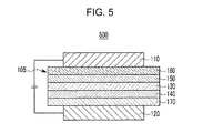
- FIGS. 1 to 5 are cross-sectional views showing exemplary embodiments of organic light emitting diodes including the exemplary embodiment of the compound for an organic optoelectronic device.
- organic light emitting diodes 100, 200, 300, 400, and 500 include at least one organic thin layer 105 interposed between an anode 120 and a cathode 110.
- the anode 120 includes an anode material, which can help injecting the holes into the organic thin layer.
- the anode material includes: a metal such as nickel, platinum, vanadium, chromium, copper, zinc, and gold, or alloys thereof; a metal oxide such as zinc oxide, indium oxide, indium tin oxide (ITO), and indium zinc oxide (IZO); a combination of a metal and oxide such as ZnO:Al and SnO 2 :Sb; or a conductive polymer such as poly(3-methylthiophene), poly[3,4-(ethylene-1,2-dioxy)thiophene] (PEDT), polypyrrole, and polyaniline, but is not limited thereto.
- a transparent electrode including indium tin oxide (ITO) as an anode.
- the cathode 110 includes a cathode material, which can help injecting electrons into the organic thin layer.
- the cathode material includes: a metal such as magnesium, calcium, sodium, potassium, titanium, indium, yttrium, lithium, gadolinium, aluminum, silver, tin, and lead, or alloys thereof; or a multi-layered material such as LiF/Al, Liq/Al, LiO 2 /Al, LiF/Ca, LiF/Al, and BaF 2 /Ca, but is not limited thereto.
- the organic light emitting diode 100 includes an organic thin layer 105 including only an emission layer 130.
- a double-layered organic light emitting diode 200 includes an organic thin layer 105 including an emission layer 230 including an electron transport layer (ETL) (not shown), and a hole transport layer (HTL) 140.
- the organic thin layer 105 includes a double layer of the emission layer 230 and the hole transport layer (HTL) 140.
- the emission layer 230 also functions as an electron transport layer (ETL), and the hole transport layer (HTL) 140 layer has an excellent binding property with a transparent electrode such as ITO or an excellent hole transport capability.
- a three-layered organic light emitting diode 300 includes an organic thin layer 105 including an electron transport layer (ETL) 150, an emission layer 130, and a hole transport layer (HTL) 140.
- the emission layer 130 is independently installed, and layers having an excellent electron transport capability or an excellent hole transport capability are separately stacked.
- a four-layered organic light emitting diode 400 includes an organic thin layer 105 including an electron injection layer (EIL) 160, an emission layer 130, a hole transport layer (HTL) 140, and a hole injection layer (HIL) 170 for adherence with the anode of ITO.
- EIL electron injection layer
- HTL hole transport layer
- HIL hole injection layer
- a five-layered organic light emitting diode 500 includes an organic thin layer 105 including an electron transport layer (ETL) 150, an emission layer 130, a hole transport layer (HTL) 140, and a hole injection layer (HIL) 170, and further includes an electron injection layer (EIL) 160 to achieve a low voltage.
- ETL electron transport layer
- HTL hole transport layer
- HIL hole injection layer
- EIL electron injection layer
- the organic thin layer 105 including at least one selected from an electron transport layer (ETL) 150, an electron injection layer (EIL) 160, emission layers 130 and 230, a hole transport layer (HTL) 140, a hole injection layer (HIL) 170, wherein the organic thin layer includes a compound for an organic optoelectronic device.
- the compound for an organic optoelectronic device may be used for an electron transport layer (ETL) 150 or electron injection layer (EIL) 160.
- ETL electron transport layer
- EIL electron injection layer
- the material for the organic photoelectric device may be included as a phosphorescent or fluorescent host or a fluorescent blue dopant.
- the organic light emitting diode may be fabricated by: forming an anode on a substrate; forming an organic thin layer in accordance with a dry coating method such as evaporation, sputtering, plasma plating, and ion plating, or a wet coating method such as spin coating, dipping, and flow coating; and providing a cathode thereon.
- a dry coating method such as evaporation, sputtering, plasma plating, and ion plating
- a wet coating method such as spin coating, dipping, and flow coating
- Another embodiment of the present disclosure provides a display device including the organic photoelectric device according to the above embodiment.
- the compound A-1 as a specific example of a compound for an organic optoelectronic device according to the present disclosure is synthesized according to the following Reaction Scheme 1.
- the separated product is recrystallized and purified under a toluene/methanol condition, obtaining 465 mg of a desired compound represented by Chemical Formula A-01 (a yield of 65 %).
- the compound A-2 as a specific example of a compound for an organic optoelectronic device according to the present disclosure is synthesized according to the following Reaction Scheme 2.
- the obtained product is recrystallized and purified under a toluene/methanol condition, obtaining 515 mg of a desired compound represented by Chemical Formula A-2 (a yield of 72 %).
- the compound A-3 as a specific example of a compound for an organic optoelectronic device according to the present disclosure is synthesized according to the following Reaction Scheme 3.
- the aqueous solution layer is removed and the organic solution layer is filtered by passing through silica gel, and then concentrated under a reduced pressure.
- the separated product is recrystallized and purified under a toluene/methanol condition, obtaining 422 mg of a desired compound represented by Chemical Formula A-3 (a yield of 59 %).
- the compound A-4 as a specific compound for an organic optoelectronic device according to the present disclosure is synthesized according to the following Reaction Scheme 4.
- the separated product is recrystallized and purified under a toluene/methanol condition, obtaining 387 mg of a compound represented by Chemical Formula A-4 (a yield of 52 %).
- the compound A-5 as specific example of a compound for an organic optoelectronic device is synthesized according to the following Reaction Scheme 5.
- the separated product is recrystallized and purified under a toluene/methanol condition, obtaining 497 mg of a compound represented by Chemical Formula A-5 (a yield of 68 %).
- the compound A-6 as a specific compound for an organic optoelectronic device according to the present disclosure is synthesized according to the following Reaction Scheme 6.
- the separated product is recrystallized and purified under a toluene/methanol condition, obtaining 386 mg of a compound represented by Chemical Formula A-6 (a yield of 54 %).
- the compound A-7 as a specific compound for an organic optoelectronic device according to the present disclosure is synthesized according to the following Reaction Scheme 7.
- the aqueous solution layer is removed and the organic solution layer is filtered by passing through silica gel, and then concentrated under a reduced pressure.
- the separated product is recrystallized and purified under a toluene/methanol condition, obtaining 444 mg of a desired compound represented by Chemical Formula A-7 (a yield of 62 %).
- the compound A-8 as a specific example of a compound for an organic optoelectronic device according to the present disclosure is synthesized according to the following Reaction Scheme 8.
- the separated product is recrystallized and purified under a toluene/methanol condition, obtaining 559 mg of a desired compound represented by Chemical Formula A-8 (a yield of 78 %).
- the host compound synthesized according to Example 1 is doped with 10 wt% of Ir(ppy) 3 , preparing a mixture for an emission layer. Then, 1 wt% of the mixture for an emission layer is dissolved in a toluene solvent, preparing a composition for an organic photoelectric device.
- a transparent electrode substrate is fabricated by coating ITO (indiumtin oxide) on a glass substrate, cleaning it, patterning the ITO using a photosensitive resin and an etchant, and cleaning it again.
- PEDOT bar 4083, Bayer Inc.
- HIL hole injection layer
- the composition for an organic photoelectric device prepared in the first step is spin-coated on the hole injection layer (HIL) and fired in a vacuum oven to completely remove a solvent and form an emission layer.
- the composition for an emission layer is filtered through a 0.2 mm filter before the spin-coating.
- the emission layer is formed to be about 45 nm thick by controlling the concentration and spin-coating speed of the composition.
- an electron transport layer (ETL) is formed by respectively vacuum-depositing ET202 and LiQ to be 15 nm thick on the emission layer with a vacuum depositor, while a vacuum degree of less than or equal to 4 X 10 -6 Torr is maintained.
- Al is sequentially deposited to be 120 nm thick to form a negative electrode on the electron transport layer (ETL). In the deposition, the thickness and speed of the negative electrode are controlled using a crystal sensor.
- the organic light emitting diode is specifically fabricated to have a structure of ITO / PEDOT:PSS (55 nm) / EML (host compound (90 wt%) + dopant compound (10 wt%), 45 nm) / ET202 (15 nm) / LiQ (15 nm) / Al (120 nm).
- An organic light emitting diode is fabricated according to the same method as Example 9, except for using the host compound synthesized according to Example 2 instead of the one according to Example 1.
- An organic light emitting diode is fabricated according to the same method as Example 9, except for using the host compound synthesized according to Example 3 instead of the one according to Example 1.
- An organic light emitting diode is fabricated according to the same method as Example 9, except for using the host compound synthesized according to Example 4 instead of the one according to Example 1.
- An organic light emitting diode is fabricated according to the same method as Example 9, except for using the host compound synthesized according to Example 5 instead of the one according to Example 1.
- An organic light emitting diode is fabricated according to the same method as Example 9, except for using the host compound synthesized according to Example 6 instead of the one according to Example 1.
- An organic light emitting diode is fabricated according to the same method as Example 9, except for using the host compound synthesized according to Example 7 instead of the one according to Example 1.
- An organic light emitting diode is fabricated according to the same method as Example 9, except for using the host compound synthesized according to Example 8 instead of the one according to Example 1.
- An organic light emitting diode is fabricated according to the same method as Example 9, except for using a mixture of PVK (polyvinylcarbazole) and PBD (2-(4-biphenyl)-5-(4-t-butylphenyl)-1,3,4-oxadiazole) represented by the following chemical formulae in a weight ratio of 1:1 as a host instead of the host compound synthesized according to Example 1.
- PVK polyvinylcarbazole
- PBD 2-(4-biphenyl)-5-(4-t-butylphenyl)-1,3,4-oxadiazole
- the Ir(ppy) 3 , PVK, and PBD used to fabricate the organic light emitting diode have the following structures.
- the obtained organic light emitting diodes are measured regarding current value flowing in a unit device, while their voltages are increased from 0 V to 10 V using a current-voltage meter (Keithley 2400).
- the measured current value is divided by an area to calculate current density.
- the organic light emitting diodes are measured regarding luminance using a luminance meter (Minolta Cs-1000A) while their voltages are increased from 0 V to 10 V.
- the host materials used in Examples 9 to 16 have excellent device performance in terms of luminous efficiency and electric power efficiency compared with the one used in Comparative Example 1.
- the host materials used in Example 14 and 15 have excellent device performance in terms of driving voltage, current efficiency, and electric power efficiency compared with the one according to Comparative Example 1. Accordingly, the host materials may realize an organic light emitting diode having a low voltage, high efficiency, high luminance, and a long life-span.
Landscapes
- Chemical & Material Sciences (AREA)
- Organic Chemistry (AREA)
- Engineering & Computer Science (AREA)
- Materials Engineering (AREA)
- Physics & Mathematics (AREA)
- Spectroscopy & Molecular Physics (AREA)
- Crystallography & Structural Chemistry (AREA)
- Inorganic Chemistry (AREA)
- Optics & Photonics (AREA)
- Electroluminescent Light Sources (AREA)
- Plural Heterocyclic Compounds (AREA)
- Photovoltaic Devices (AREA)
- Devices For Indicating Variable Information By Combining Individual Elements (AREA)
Abstract

Description
- A compound for an organic optoelectronic device being capable of providing an organic optoelectronic device having excellent life-span, efficiency, electrochemical stability, and thermal stability, an organic light emitting diode including the compound, and a display device including the organic light emitting diode are disclosed.
- An organic optoelectronic device is, in a broad sense, a device for transforming photo-energy to electrical energy, or conversely, a device for transforming electrical energy to photo-energy.
- An organic optoelectronic device may be classified in accordance with its driving principles. A first organic optoelectronic device is an electronic device driven as follows: excitons are generated in an organic material layer by photons from an external light source; the excitons are separated into electrons and holes; and the electrons and holes are transferred to different electrodes as a current source (voltage source).
- A second organic optoelectronic device is an electronic device driven as follows: a voltage or a current is applied to at least two electrodes to inject holes and/or electrons into an organic semiconductor positioned at an interface of the electrodes, and the device is driven by the injected electrons and holes.
- Examples of the organic optoelectronic device include an organic light emitting diode, an organic solar cell, an organic photoconductor drum, an organic transistor, and the like, which require a hole injecting or transport material, an electron injecting or transport material, or a light emitting material.
- Particularly, an organic light emitting diode (OLED) has recently drawn attention due to an increasing demand for flat panel displays. In general, organic light emission refers to conversion of electrical energy into photo-energy.
- An organic light emitting diode can convert electrical energy into light by applying current to an organic light emitting material. It has a structure in which a functional organic material layer is interposed between an anode and a cathode. The organic material layer includes a multi-layer including different materials, for example a hole injection layer (HIL), a hole transport layer (HTL), an emission layer, an electron transport layer (ETL), and an electron injection layer (EIL), in order to improve efficiency and stability of an organic light emitting diode.
- In such an organic light emitting diode, when a voltage is applied between an anode and a cathode, holes from the anode and electrons from the cathode are injected to an organic material layer and recombined to generate excitons having high energy. The generated excitons generate light having certain wavelengths while shifting to a ground state.
- Recently, it has become known that a phosphorescent light emitting material may be used as a light emitting material of an organic light emitting diode in addition to the fluorescent light emitting material. Such a phosphorescent material emits lights by first transporting the electrons from a ground state to an exited state, then transiting a singlet exciton to a triplet exciton through intersystem crossing, and finally transiting a triplet exciton to a ground state to emit light.
- In an organic light emitting diode, an organic material layer includes a light emitting material and a charge transport material, for example a hole injection material, a hole transport material, an electron transport material, an electron injection material, and the like.
- The light emitting material is classified as blue, green, and red light emitting materials according to emitted colors, and yellow and orange light emitting materials which emit colors approaching natural colors.
- When a material is used as a light emitting material, its maximum light emitting wavelength can be shifted to a long wavelength or its color purity can decrease because of interactions between molecules. In addition, device efficiency can decrease because of a light emitting quenching effect. Therefore, a host/dopant system is included for a light emitting material in order to improve color purity and increase luminous efficiency and stability through energy transfer.
- In order to achieve excellent performance of an organic light emitting diode, a material for an organic material layer, for example a hole injection material, a hole transport material, an electron transport material, an electron injection material, and a light emitting material such as a host and/or a dopant, should be stable and have good efficiency. However, development of such a material has thus far been elusive and there is still a need for an improved material for an organic light emitting diode and other organic optoelectronic devices.
- A low molecular organic light emitting diode is manufactured as a thin film in a vacuum deposition method, and can have good efficiency and life-span. A polymer organic light emitting diode manufactured in an Inkjet or spin coating method has an advantage of low initial cost and being large-sized.
- Both low molecular organic light emitting and polymer organic light emitting diodes have an advantage of self-light emitting, high speed response, wide viewing angle, ultra-thinness, high image quality, durability, large driving temperature range, and the like. In particular, they have good visibility due to the self-light emitting characteristic. Compared with a liquid crystal display ("LCD"), an organic light emitting diode ("OLED") can be up to about one third thinner and lighter, because they do not need a backlight.
- In addition, since they have a response speed of a microsecond unit, which is 1000 times faster than an LCD, they can realize a motion picture without an after-image. Based on these advantages, they have been remarkably developed to be 80 times more efficient and to have a 100 times longer life-span since they first came out in the late 1980's. Recently, they have become rapidly larger such that a 40-inch organic light emitting diode panel is now possible.
- In order for the organic light emitting diode panel to be larger, it is necessary that the organic light emitting diodes have improved luminous efficiency and improved life-span at the same time. Luminous efficiency requires smooth combination between holes and electrons in an emission layer. However, since an organic material in general has slower electron mobility than hole mobility, it has a drawback of inefficient combination between holes and electrons. Accordingly, increasing electron injection and mobility from a cathode and simultaneously preventing movement of holes is required.
- In order to improve the life-span, it is required to prevent material crystallization caused by Joule heat generated during device operation. Accordingly, there has been a strong need for an organic compound having excellent electron injection and mobility, and high electrochemical stability.
- A compound for an organic optoelectronic device that may act as a light emitting or electron injection and/or transport material, and also act as a light emitting host along with an appropriate dopant, is provided.
- An organic light emitting diode having excellent life-span, efficiency, driving voltage, electrochemical stability, and thermal stability and a display device including the same are provided.
- In one embodiment, a compound for an organic optoelectronic device represented by Chemical Formula 1 is provided.

- In Chemical Formula 1, X1 to X3 are independently -C(R')- or -N-, provided that at least one of X1 to X3 is -N-, X4 is a single bond, -C(R')(R")-, -O-, -S-, -S(=O)-,-S(=O)2-, -Si(R')(R")-, or -C(=O)-, R1 to R4, R', and R" are independently hydrogen, deuterium, a halogen, a cyano group, a hydroxyl group, an amino group, a substituted or unsubstituted C1 to C20 amine group, a nitro group, a carboxyl group, a ferrocenyl group, a substituted or unsubstituted C1 to C20 alkyl group, a substituted or unsubstituted C6 to C30 aryl group, a substituted or unsubstituted C2 to C30 heteroaryl group, a substituted or unsubstituted C1 to C20 alkoxy group, a substituted or unsubstituted C6 to C20 aryloxy group, a substituted or unsubstituted C3 to C40 silyloxy group, a substituted or unsubstituted C1 to C20 acyl group, a substituted or unsubstituted C2 to C20 alkoxycarbonyl group, a substituted or unsubstituted C2 to C20 acyloxy group, a substituted or unsubstituted C2 to C20 acylamino group, a substituted or unsubstituted C2 to C20 alkoxycarbonylamino group, a substituted or unsubstituted C7 to C20 aryloxycarbonylamino group, a substituted or unsubstituted C1 to C20 sulfamoylamino group, a substituted or unsubstituted C1 to C20 sulfonyl group, a substituted or unsubstituted C1 to C20 alkylthiol group, a substituted or unsubstituted C6 to C20 arylthiol group, a substituted or unsubstituted C1 to C20 heterocyclothiol group, a substituted or unsubstituted C1 to C20 ureide group, a substituted or unsubstituted C3 to C40 silyl group, or a combination thereof, L is a substituted or unsubstituted C2 to C20 alkenylene group, a substituted or unsubstituted C2 to C20 alkynylene group, a substituted or unsubstituted C6 to C30 arylene group, a substituted or unsubstituted C2 to C30 heteroarylene group, or a combination thereof, and Ar1 and Ar2 are independently a substituted or unsubstituted C6 to C30 aryl group or a substituted or unsubstituted C2 to C30 heteroaryl group.
- The X4 may be a single bond.
- The X4 may be -C(R')(R")-.
- The X4 may be -O-.
- The X4 may be -S-.
- The X4 may be -S(=O)-.
- The X4 may be -S(=O)2-.
- The X4 may be -Si(R')(R")-.
- The X4 may be -C(=O)-.
- The compound for an organic optoelectronic device may be represented by Chemical Formula 2.

- In Chemical Formula 2, X1 to X3 are independently -C(R')- or -N-, provided that at least one of X1 to X3 is N, X4 is a single bond, -C(R')(R")-, -O-, -S-, -S(=O)-,-S(=O)2-, -Si(R')(R")-, or -C(=O)-, R1 to R4, R', and R" are independently hydrogen, deuterium, a halogen, a cyano group, a hydroxyl group, an amino group, a substituted or unsubstituted C1 to C20 amine group, a nitro group, a carboxyl group, a ferrocenyl group, a substituted or unsubstituted C1 to C20 alkyl group, a substituted or unsubstituted C6 to C30 aryl group, a substituted or unsubstituted C2 to C30 heteroaryl group, a substituted or unsubstituted C1 to C20 alkoxy group, a substituted or unsubstituted C6 to C20 aryloxy group, a substituted or unsubstituted C3 to C40 silyloxy group, a substituted or unsubstituted C1 to C20 acyl group, a substituted or unsubstituted C2 to C20 alkoxycarbonyl group, a substituted or unsubstituted C2 to C20 acyloxy group, a substituted or unsubstituted C2 to C20 acylamino group, a substituted or unsubstituted C2 to C20 alkoxycarbonylamino group, a substituted or unsubstituted C7 to C20 aryloxycarbonylamino group, a substituted or unsubstituted C1 to C20 sulfamoylamino group, a substituted or unsubstituted C1 to C20 sulfonyl group, a substituted or unsubstituted C1 to C20 alkylthiol group, a substituted or unsubstituted C6 to C20 arylthiol group, a substituted or unsubstituted C1 to C20 heterocyclothiol group, a substituted or unsubstituted C1 to C20 ureide group, a substituted or unsubstituted C3 to C40 silyl group, or a combination thereof, and Ar1 and Ar2 are independently a substituted or unsubstituted C6 to C30 aryl group or a substituted or unsubstituted C2 to C30 heteroaryl group.
- The compound for an organic optoelectronic device may be represented by Chemical Formula 3.

- In Chemical Formula 3, X1 to X3 are independently -C(R')- or -N-, provided that at least one of X1 to X3 is -N-, X4 is a single bond, -C(R')(R")-, -O-, -S-, -S(=O)-,-S(=O)2-, -Si(R')(R")-, or -C(=O)-, R1 to R4, R', and R" are independently hydrogen, deuterium, a halogen, a cyano group, a hydroxyl group, an amino group, a substituted or unsubstituted C1 to C20 amine group, a nitro group, a carboxyl group, a ferrocenyl group, a substituted or unsubstituted C1 to C20 alkyl group, a substituted or unsubstituted C6 to C30 aryl group, a substituted or unsubstituted C2 to C30 heteroaryl group, a substituted or unsubstituted C1 to C20 alkoxy group, a substituted or unsubstituted C6 to C20 aryloxy group, a substituted or unsubstituted C3 to C40 silyloxy group, a substituted or unsubstituted C1 to C20 acyl group, a substituted or unsubstituted C2 to C20 alkoxycarbonyl group, a substituted or unsubstituted C2 to C20 acyloxy group, a substituted or unsubstituted C2 to C20 acylamino group, a substituted or unsubstituted C2 to C20 alkoxycarbonylamino group, a substituted or unsubstituted C7 to C20 aryloxycarbonylamino group, a substituted or unsubstituted C1 to C20 sulfamoylamino group, a substituted or unsubstituted C1 to C20 sulfonyl group, a substituted or unsubstituted C1 to C20 alkylthiol group, a substituted or unsubstituted C6 to C20 arylthiol group, a substituted or unsubstituted C1 to C20 heterocyclothiol group, a substituted or unsubstituted C1 to C20 ureide group, a substituted or unsubstituted C3 to C40 silyl group, or a combination thereof, and Ar1 and Ar2 are independently a substituted or unsubstituted C6 to C30 aryl group or a substituted or unsubstituted C2 to C30 heteroaryl group.
- The compound for an organic optoelectronic device may be represented by Chemical Formula 4.

- In Chemical Formula 4, X1 to X3 are independently -C(R')- or -N-, provided that at least one of X1 to X3 is -N-, X4 is a single bond, -C(R')(R")-, -O-, -S-, -S(=O)-,-S(=O)2-, -Si(R')(R")-, or -C(=O)-, R1 to R4, R', and R" are independently hydrogen, deuterium, a halogen, a cyano group, a hydroxyl group, an amino group, a substituted or unsubstituted C1 to C20 amine group, a nitro group, a carboxyl group, a ferrocenyl group, a substituted or unsubstituted C1 to C20 alkyl group, a substituted or unsubstituted C6 to C30 aryl group, a substituted or unsubstituted C2 to C30 heteroaryl group, a substituted or unsubstituted C1 to C20 alkoxy group, a substituted or unsubstituted C6 to C20 aryloxy group, a substituted or unsubstituted C3 to C40 silyloxy group, a substituted or unsubstituted C1 to C20 acyl group, a substituted or unsubstituted C2 to C20 alkoxycarbonyl group, a substituted or unsubstituted C2 to C20 acyloxy group, a substituted or unsubstituted C2 to C20 acylamino group, a substituted or unsubstituted C2 to C20 alkoxycarbonylamino group, a substituted or unsubstituted C7 to C20 aryloxycarbonylamino group, a substituted or unsubstituted C1 to C20 sulfamoylamino group, a substituted or unsubstituted C1 to C20 sulfonyl group, a substituted or unsubstituted C1 to C20 alkylthiol group, a substituted or unsubstituted C6 to C20 arylthiol group, a substituted or unsubstituted C1 to C20 heterocyclothiol group, a substituted or unsubstituted C1 to C20 ureide group, a substituted or unsubstituted C3 to C40 silyl group, or a combination thereof, and Ar1 and Ar2 are independently a substituted or unsubstituted C6 to C30 aryl group or a substituted or unsubstituted C2 to C30 heteroaryl group.
- The compound for an organic optoelectronic device may be represented by Chemical Formula 5.


- In Chemical Formula 5, X1 to X3 are independently -C(R')- or -N-, provided that at least one of X1 to X3 is -N-, X4 is a single bond, -C(R')(R")-, -O-, -S-, -S(=O)-,-S(=O)2-, -Si(R')(R")-, or -C(=O)-, R1 to R4, R', and R" are independently hydrogen, deuterium, a halogen, a cyano group, a hydroxyl group, an amino group, a substituted or unsubstituted C1 to C20 amine group, a nitro group, a carboxyl group, a ferrocenyl group, a substituted or unsubstituted C1 to C20 alkyl group, a substituted or unsubstituted C6 to C30 aryl group, a substituted or unsubstituted C2 to C30 heteroaryl group, a substituted or unsubstituted C1 to C20 alkoxy group, a substituted or unsubstituted C6 to C20 aryloxy group, a substituted or unsubstituted C3 to C40 silyloxy group, a substituted or unsubstituted C1 to C20 acyl group, a substituted or unsubstituted C2 to C20 alkoxycarbonyl group, a substituted or unsubstituted C2 to C20 acyloxy group, a substituted or unsubstituted C2 to C20 acylamino group, a substituted or unsubstituted C2 to C20 alkoxycarbonylamino group, a substituted or unsubstituted C7 to C20 aryloxycarbonylamino group, a substituted or unsubstituted C1 to C20 sulfamoylamino group, a substituted or unsubstituted C1 to C20 sulfonyl group, a substituted or unsubstituted C1 to C20 alkylthiol group, a substituted or unsubstituted C6 to C20 arylthiol group, a substituted or unsubstituted C1 to C20 heterocyclothiol group, a substituted or unsubstituted C1 to C20 ureide group, a substituted or unsubstituted C3 to C40 silyl group, or a combination thereof, and Ar1 and Ar2 are independently a substituted or unsubstituted C6 to C30 aryl group or a substituted or unsubstituted C2 to C30 heteroaryl group.
- The compound for an organic optoelectronic device may be represented by the Chemical Formula 6.

- In Chemical Formula 6, X1 to X3 are independently -C(R')- or -N-, provided that at least one of X1 to X3 is -N-, R1 to R4 and R' are independently hydrogen, deuterium, a halogen, a cyano group, a hydroxyl group, an amino group, a substituted or unsubstituted C1 to C20 amine group, a nitro group, a carboxyl group, a ferrocenyl group, a substituted or unsubstituted C1 to C20 alkyl group, a substituted or unsubstituted C6 to C30 aryl group, a substituted or unsubstituted C2 to C30 heteroaryl group, a substituted or unsubstituted C1 to C20 alkoxy group, a substituted or unsubstituted C6 to C20 aryloxy group, a substituted or unsubstituted C3 to C40 silyloxy group, a substituted or unsubstituted C1 to C20 acyl group, a substituted or unsubstituted C2 to C20 alkoxycarbonyl group, a substituted or unsubstituted C2 to C20 acyloxy group, a substituted or unsubstituted C2 to C20 acylamino group, a substituted or unsubstituted C2 to C20 alkoxycarbonylamino group, a substituted or unsubstituted C7 to C20 aryloxycarbonylamino group, a substituted or unsubstituted C1 to C20 sulfamoylamino group, a substituted or unsubstituted C1 to C20 sulfonyl group, a substituted or unsubstituted C1 to C20 alkylthiol group, a substituted or unsubstituted C6 to C20 arylthiol group, a substituted or unsubstituted C1 to C20 heterocyclothiol group, a substituted or unsubstituted C1 to C20 ureide group, a substituted or unsubstituted C3 to C40 silyl group, or a combination thereof, and Ar1 and Ar2 are independently a substituted or unsubstituted C6 to C30 aryl group or a substituted or unsubstituted C2 to C30 heteroaryl group.
- The Ar1 and Ar2 may be independently a substituted or unsubstituted C6 to C30 aryl group.
- The X1 to X3 may be independently CR' or N, and at least two of the X1 to X3 are N.
- The compound for an organic optoelectronic device may be represented by one of Chemical Formulae A-1 to A-140.


- The organic optoelectronic device may be selected from an organic photoelectric device, an organic light emitting diode, an organic solar cell, an organic transistor, an organic photoconductor drum, and an organic memory device.
- According to another embodiment, an organic light emitting diode including an anode, a cathode, and at least one organic thin layer between the anode and the cathode is provided. At least one organic thin layer includes the compound for an organic optoelectronic device described above.
- The organic thin layer may be selected from an emission layer, a hole transport layer (HTL), a hole injection layer (HIL), an electron transport layer (ETL), an electron injection layer (EIL), a hole blocking layer, and a combination thereof.
- The compound for an organic optoelectronic device may be included in an emission layer.
- The compound for an organic photoelectric device may be used as a phosphorescent or fluorescent host material in an emission layer.
- According to yet another embodiment, a display device including the organic light emitting diode is provided.
- The above and other aspects, advantages and features of this disclosure will become more apparent by describing in further detail exemplary embodiments thereof with reference to the accompanying drawings, in which:
-
FIGS. 1 to 5 are cross-sectional views showing exemplary embodiments of organic light emitting diodes including an exemplary embodiment of a compound for an organic optoelectronic device; and -
FIG. 6 shows examples of compounds for an organic optoelectronic device according to an embodiment. - Exemplary embodiments will hereinafter be described in detail. However, these embodiments are only exemplary, and the present disclosure is not limited thereto but rather is defined by the scope of the appended claims.
- It will be understood that when an element is referred to as being "on" another element, it may be directly on the other element or intervening elements may be present therebetween. In contrast, when an element is referred to as being "directly on" another element, there are no intervening elements present. It will be understood that, although the terms first, second, third etc. may be used herein to describe various elements, components, regions, layers and/or sections, there elements, components, regions, layers and/or sections should not be limited by these terms. These terms are only used to distinguish one element, component, region, layer or section from another element, component, region, layer, or section. Thus, a first element, component, region, layer, or section discussed below could be termed a second element, component, region, layer, or section without departing from the teachings of the present embodiments.
- The terminology used herein is for the purpose of describing particular embodiments only and is not intended to be limiting. As used herein, the singular forms "a", "an" and "the" are intended to include the plural forms as well, unless the context clearly indicates otherwise. The term "or" means "and/or." As used herein, the term "and/or" includes any and all combinations of one or more of the associated listed items. Expressions such as "at least one of," when preceding a list of elements, modify the entire list of elements and do not modify the individual elements of the list.
- It will be further understood that the terms "comprises" and/or "comprising," or "includes" and/or "including" when used in this specification, specify the presence of stated features, regions, integers, steps, operations, elements, and/or components, but do not preclude the presence or addition of one or more other features, regions, integers, steps, operations, elements, components, and/or groups thereof.
- Unless otherwise defined, all terms (including technical and scientific terms) used herein have the same meaning as commonly understood by one of ordinary skill in the art to which this general inventive concept belongs. It will be further understood that terms, such as those defined in commonly used dictionaries, should be interpreted as having a meaning that is consistent with their meaning in the context of the relevant art and the present disclosure, and will not be interpreted in an idealized or overly formal sense unless expressly so defined herein.
- Exemplary embodiments are described herein with reference to cross section illustrations that are schematic illustrations of idealized embodiments. As such, variations from the shapes of the illustrations as a result, for example, of manufacturing techniques and/or tolerances, are to be expected. Thus, embodiments described herein should not be construed as limited to the particular shapes of regions as illustrated herein but are to include deviations in shapes that result, for example, from manufacturing. For example, a region illustrated or described as flat may typically have rough and/or nonlinear features. Moreover, sharp angles that are illustrated may be rounded. Thus, the regions illustrated in the figures are schematic in nature and their shapes are not intended to illustrate the precise shape of a region and are not intended to limit the scope of the present claims.
- As used herein, when specific definition is not otherwise provided, the term "substituted" refers to a group or moiety substituted with deuterium, a halogen, a hydroxy group, an amino group, a substituted or unsubstituted C1 to C30 amine group, a nitro group, a substituted or unsubstituted C3 to C40 silyl group, a C1 to C30 alkyl group, a C1 to C10 alkylsilyl group, a C3 to C30 cycloalkyl group, a C6 to C30 aryl group, a C1 to C20 alkoxy group, a fluoro group, a C1 to C10 trifluoroalkyl group such as a trifluoromethyl group, and the like, or a cyano group instead of at least one hydrogen of a substituting group or compound.
- Two adjacent substituents may be selected from an amino group, a substituted or unsubstituted C1 to C20 amine group, a nitro, a substituted or unsubstituted C3 to C40 silyl group, a C1 to C30 alkyl group, a C1 to C10 alkylsilyl group, a C3 to C30 cycloalkyl group, a C6 to C30 aryl group, a C1 to C20 alkoxy group, or a trifluoroalkyl group such as a trifluoromethyl group, and the two substituents may be fused to each other to provide a ring having 3 to 8 atoms in the ring.
- As used herein, when specific definition is not otherwise provided, the term "hetero" refers to a substituent, group, or compound including 1 to 3 hetero atoms selected from N, O, S, and P, and remaining carbons in one functional group.
- As used herein, when a definition is not otherwise provided, the term "combination thereof" when used in the context of substituents or groups refers to at least two substituents or groups bound to each other by a linker, or at least two substituents or groups condensed to each other.
- In the specification, when a definition is not otherwise provided, the term "alkyl group" may refer to an aliphatic hydrocarbon group. The alkyl group may be a saturated group without any alkene group or alkyne group.
- The alkyl group may be branched, linear, or cyclic. The alkyl group may have the specified number of carbon atoms. More specifically, the alkyl group may be a C1 to C10 alkyl group or a C1 to C6 alkyl group. For example, the C1 to C4 alkyl group may have 1 to 4 carbon atoms, and may be selected from methyl, ethyl, propyl, iso-propyl, n-butyl, iso-butyl, sec-butyl, and t-butyl. Examples of the alkyl group may be a methyl group, an ethyl group, a propyl group, an isopropyl group, a butyl group, an isobutyl group, a t-butyl group, a pentyl group, a hexyl group, a cyclopropyl group, a cyclobutyl group, a cyclopentyl group, a cyclohexyl group, and the like.
- The "alkenyl group" may refer to a substituent of at least one carbon-carbon double bond of at least two carbons.
- The "alkynyl group" may refer to a substituent of at least one carbon-carbon triple bond of at least two carbons.
- The term "alkenylene group" may refer to a straight or branched chain, divalent hydrocarbon group having at least one carbon-carbon double bond (e.g., ethenylene (-HC=CH-)).
- The term "alkylene group" may refer to a straight or branched chain, saturated, divalent aliphatic hydrocarbon group, (e.g., methylene (-CH2-) or, propylene (-(CH2)3-)).
- The term "aromatic group" may refer to a substituent including all elements of the cycle having p-orbitals which form conjugation. Examples may include an aryl group and a heteroaryl group.
- The "aryl group" may refer to a monocyclic or fused ring polycyclic (i.e., rings sharing adjacent pairs of carbon atoms) substituent.
- The term "heteroaryl group" may refer to an aryl group including 1 to 3 hetero atoms selected from N, O, S, and P as ring member(s). The heteroaryl group may be a fused ring cyclic group where each cycle may include the 1 to 3 heteroatoms.
- The term "arylene group" may refer to a divalent group formed by the removal of two hydrogen atoms from one or more rings of an arene, wherein the hydrogen atoms may be removed from the same or different rings (e.g., phenylene or napthylene).
- The term "heteroarylene group" may refer to a divalent radical formed by the removal of two hydrogen atoms from one or more rings of a heteroaryl moiety, wherein the hydrogen atoms may be removed from the same or different rings (preferably the same ring), each of which rings may be aromatic or nonaromatic.
- The term "alkoxy group" may refer to an alkyl group that is linked via an oxygen (i.e., alkyl-O-), for example methoxy, ethoxy, and sec-butyloxy groups.
- The term "aryloxy group" may refer to an aryl group that is linked via an oxygen (i.e., aryl-O-).
- The term "silyl group" may refer to -SiR3 wherein each R is independently a substituted or unsubstituted alkyl.
- The term "silyloxy group" may refer to a silyl group that is linked via an oxygen (i.e., silyl-O-).
- The term "alkoxycarbonylamino group" may refer to a group represented by-NHCOO-alkyl in which alkyl is as defined herein.
- The term "aryloxycarbonylamino group" may refer to a group represented by -NHCOO-aryl in which aryl is as defined herein.
- The term "alkoxycarbonyl group" may refer to an -C(O)-O-alkyl group in which alkyl is as defined herein.
- The term "acyl group" may refer to the group -C(O)-R where R is H, C1-C20 alkyl, C2-C20 alkenyl, C2-C20 alkynyl, heterocycloalkyl, aryl, heteroaryl, alkyl aryl, alkyl heteroaryl, alkenyl aryl, alkenyl heteroaryl, alkynyl aryl, alkynyl heteroaryl.
- The term "heterocycloalkyl" may refer to a non-aromatic monocyclic or polycyclic ring comprising carbon and hydrogen atoms and at least one heteroatom ring member.
- The term "alkyl aryl" may refer to an alkyl group covalently linked to a substituted or unsubstituted aryl group that is linked to a compound.
- The term "alkyl heteroaryl" may refer to an alkyl group covalently linked to a substituted or unsubstituted heteroaryl group that is linked to a compound.
- The term "alkenyl aryl" may refer to an alkenyl group covalently linked to a substituted or unsubstituted aryl group that is linked to a compound.
- The term "alkenyl heteroaryl" may refer to an alkenyl group covalently linked to a substituted or unsubstituted heteroaryl group that is linked to a compound.
- The term "alkynyl aryl" may refer to an alkynyl group covalently linked to a substituted or unsubstituted aryl group that is linked to a compound.
- The term "alkynyl heteroaryl" may refer to an alkynyl group covalently linked to a substituted or unsubstituted heteroaryl group that is linked to a compound.
- The term "acyloxy group" may refer to a group represented by -OC(O)R where R is H, C1-C20 alkyl, C2-C20 alkenyl, C2-C20 alkynyl, heterocycloalkyl, aryl, heteroaryl, alkyl aryl, alkyl heteroaryl, alkenyl aryl, alkenyl heteroaryl, alkynyl aryl, alkynyl heteroaryl.
- The term "acylamino group" may refer to a group represented by -NRC(O)R' where each R and R' is independently H, C1-C20 alkyl, C2-C20 alkenyl, C2-C20 alkynyl, heterocycloalkyl, aryl, heteroaryl, alkyl aryl, alkyl heteroaryl, alkenyl aryl, alkenyl heteroaryl, alkynyl aryl, alkynyl heteroaryl.
- The term "sulfonyl group" may refer to a group represented by -SO2-R wherein R is selected from H, aryl, heteroaryl, C1 to C20 alkyl, C1 to C20 alkyl substituted with halogens, C2-C20 alkenyl, C2-C20 alkynyl, heterocycloalkyl, aryl, heteroaryl, alkyl aryl, alkyl heteroaryl, alkenyl aryl, alkenyl heteroaryl, alkynyl aryl, alkynyl heteroaryl.
- The term "sulfamoylamino group" may refer to a group represented by -NH-SO2-NR1R2, wherein R1 and R2 are independently hydrogen, an alkyl or an aryl.
- The term "alkylthiol" may refer to -alkyl-SH in which alkyl is as defined herein.
- The term "arylthiol" may refer to -aryl-SH in which aryl is as defined herein.
- The term "heterocyclothiol" may refer to -heterocyclic group-SH in which heterocyclic group is a monocyclic or polycyclic ring comprising at least one heteroatom ring member.
- The term "ureide" may refer to the group -C(O)NRC(O)NR'R" where each R, R', R" is independently H, C1-C20 alkyl, C2-C20 alkenyl, C2-C20 alkynyl, heterocycloalkyl, aryl, heteroaryl, alkyl aryl, alkyl heteroaryl, alkenyl aryl, alkenyl heteroaryl, alkynyl aryl, alkynyl heteroaryl.
- The term "amino" as used herein may refer to a group of the formula (-NH2).
- The term "substituted or unsubstituted C1 to C20 amine group" as used herein may refer to a group of the formula -N(R)2, wherein one R group may be hydrogen, and the other or both R groups may be the same or different substituted or unsubstituted C1-C20 alkyl or C6-C20 aryl.
- In this specification, the term "hole properties" may refer to a characteristic that a hole formed in the positive electrode is easily injected into the emission layer and transported in the emission layer due to a conductive characteristic according to HOMO level. More specifically, the hole properties are similar to electron-repelling properties.
- In this specification, the term "electronic properties" may refer to a characteristic that an electron formed in the negative electrode is easily injected into the emission layer and transported in the emission layer due to a conductive characteristic according to LUMO level. More specifically, the electronic properties are similar to electron-attracting properties.
- A compound for an organic optoelectronic device according to an embodiment has a structure including two fused rings linked to a phenylene core. The structure may selectively include various substituents.
- The compound may be used a light emitting material, a hole injection material, or a hole transport material of an organic optoelectronic device. Particularly, it may be adapted for use as an electron injection material or an electron transport material.
- The compound for an organic optoelectronic device includes a core part and various substituents for substituting the core part, and thus may have various energy band gaps.
- The compound may have an appropriate energy level depending on the substituents, and thus may fortify electron transport capability and hole transport capability of an organic optoelectronic device and bring about excellent effects in terms of efficiency and driving voltage, and may also have excellent electrochemical and thermal stability and thus improve life-span characteristics during the operation of the organic optoelectronic device.
- According to an embodiment, a compound for an organic optoelectronic device represented by the following Chemical Formula 1 is provided.

- In Chemical Formula 1, X1 to X3 are independently -C(R')- or -N-, provided that at least one of X1 to X3 is -N-, X4 is a single bond, -C(R')(R")-, -O-, -S-, -S(=O)-,-S(=O)2-, -Si(R')(R")-, or -C(=O)-, R1 to R4, R', and R" are independently hydrogen, deuterium, a halogen, a cyano group, a hydroxyl group, an amino group, a nitro group, a carboxyl group, a ferrocenyl group, a substituted or unsubstituted C1 to C20 alkyl group, a substituted or unsubstituted C6 to C30 aryl group, a substituted or unsubstituted C2 to C30 heteroaryl group, a substituted or unsubstituted C1 to C20 alkoxy group, a substituted or unsubstituted C6 to C20 aryloxy group, a substituted or unsubstituted C3 to C40 silyloxy group, a substituted or unsubstituted C1 to C20 acyl group, a substituted or unsubstituted C2 to C20 alkoxycarbonyl group, a substituted or unsubstituted C2 to C20 acyloxy group, a substituted or unsubstituted C2 to C20 acylamino group, a substituted or unsubstituted C2 to C20 alkoxycarbonylamino group, a substituted or unsubstituted C7 to C20 aryloxycarbonylamino group, a substituted or unsubstituted C1 to C20 sulfamoylamino group, a substituted or unsubstituted C1 to C20 sulfonyl group, a substituted or unsubstituted C1 to C20 alkylthiol group, a substituted or unsubstituted C6 to C20 arylthiol group, a substituted or unsubstituted C1 to C20 heterocyclothiol group, a substituted or unsubstituted C1 to C20 ureide group, a substituted or unsubstituted C3 to C40 silyl group, or a combination thereof, L is a substituted or unsubstituted C2 to C20 alkenylene group, a substituted or unsubstituted C2 to C20 alkynylene group, a substituted or unsubstituted C6 to C30 arylene group, a substituted or unsubstituted C2 to C30 heteroarylene group, or a combination thereof, and Ar1 and Ar2 are independently a substituted or unsubstituted C6 to C30 aryl group or a substituted or unsubstituted C2 to C30 heteroaryl group.
- The X4 may be selected from the above examples depending on desired characteristics of the compound.
- Specific examples of the Ar1 and Ar2 are independently a substituted or unsubstituted phenyl group, a substituted or unsubstituted naphthyl group, a substituted or unsubstituted anthracenyl group, a substituted or unsubstituted phenanthryl group, a substituted or unsubstituted naphthacenyl group, a substituted or unsubstituted pyrenyl group, a substituted or unsubstituted biphenylyl group, a substituted or unsubstituted p-terphenyl group, a substituted or unsubstituted m-terphenyl group, a substituted or unsubstituted chrysenyl group, a substituted or unsubstituted triphenylenyl group, a substituted or unsubstituted perylenyl group, a substituted or unsubstituted indenyl group, a substituted or unsubstituted furanyl group, a substituted or unsubstituted thiophenyl group, a substituted or unsubstituted pyrrolyl group, a substituted or unsubstituted pyrazolyl group, a substituted or unsubstituted imidazolyl group, a substituted or unsubstituted triazolyl group, a substituted or unsubstituted oxazolyl group, a substituted or unsubstituted thiazolyl group, a substituted or unsubstituted oxadiazolyl group, a substituted or unsubstituted thiadiazolyl group, a substituted or unsubstituted pyridyl group, a substituted or unsubstituted pyrimidinyl group, a substituted or unsubstituted pyrazinyl group, a substituted or unsubstituted triazinyl group, a substituted or unsubstituted benzofuranyl, a substituted or unsubstituted benzothiophenyl group, a substituted or unsubstituted benzimidazolyl group, a substituted or unsubstituted indolyl group, a substituted or unsubstituted quinolinyl group, a substituted or unsubstituted isoquinolinyl group, a substituted or unsubstituted quinazolinyl group, a substituted or unsubstituted quinoxalinyl group, a substituted or unsubstituted naphthyridinyl group, a substituted or unsubstituted benzoxazinyl group, a substituted or unsubstituted benzthiazinyl group, a substituted or unsubstituted acridinyl group, a substituted or unsubstituted phenazinyl group, a substituted or unsubstituted phenothiazinyl group, a substituted or unsubstituted phenoxazinyl group, or a combination thereof, but are not limited thereto.
- A total conjugation length of the compound may be controlled by selecting L appropriately, and thereby bandgap of triplet energy may be adjusted. Accordingly, a material needed for an organic optoelectronic device may be realized. In addition, ortho, para, or meta binding positions may adjust the triplet energy bandgap.
- Examples of the L may include a substituted or unsubstituted phenylene group, a substituted or unsubstituted biphenylene group, a substituted or unsubstituted terphenylene group, a substituted or unsubstituted naphthylene group, a substituted or unsubstituted anthracenylene group, a substituted or unsubstituted phenanthrylene group, a substituted or unsubstituted pyrenylene group, a substituted or unsubstituted fluorenylene group, a substituted or unsubstituted p-terphenylene group, a substituted or unsubstituted m-terphenylene group, a substituted or unsubstituted pyrenylene group, and the like.
- More specifically, the L may be a substituted or unsubstituted C2 to C30 heteroarylene group.
- Examples of the substituted or unsubstituted C2 to C30 heteroarylene group may include a quinolinylene group, an isoquinolinylene group, a pyridinylene group, a pyrimidinylene group, a triazinylene group, a pyrrolylene group, a pyrazolylene group, an imidazolylene group, an imidazoliylene group, a pyrazinylene group, an indolylene group, a furylylene group, an indazolylene group, a thiophenylene group, a benzothiophenylene group, an isothiazolylene group, and the like.
- The compound for an organic optoelectronic device may be represented by the following Chemical Formula 2.


- In Chemical Formula 2, X1 to X3 are independently -C(R')- or -N-, provided that at least one of X1 to X3 is -N-, X4 is a single bond, -C(R')( R")-, -O-, -S-, -S(=O)-, -S(=O)2-, -SiR'R"-, or -C(=O)-, R1 to R4, R', and R" are independently hydrogen, deuterium, a halogen, a cyano group, a hydroxyl group, an amino group, a nitro group, a carboxyl group, a ferrocenyl group, a substituted or unsubstituted C1 to C20 alkyl group, a substituted or unsubstituted C6 to C30 aryl group, a substituted or unsubstituted C2 to C30 heteroaryl group, a substituted or unsubstituted C1 to C20 alkoxy group, a substituted or unsubstituted C6 to C20 aryloxy group, a substituted or unsubstituted C3 to C40 silyloxy group, a substituted or unsubstituted C1 to C20 acyl group, a substituted or unsubstituted C2 to C20 alkoxycarbonyl group, a substituted or unsubstituted C2 to C20 acyloxy group, a substituted or unsubstituted C2 to C20 acylamino group, a substituted or unsubstituted C2 to C20 alkoxycarbonylamino group, a substituted or unsubstituted C7 to C20 aryloxycarbonylamino group, a substituted or unsubstituted C1 to C20 sulfamoylamino group, a substituted or unsubstituted C1 to C20 sulfonyl group, a substituted or unsubstituted C1 to C20 alkylthiol group, a substituted or unsubstituted C6 to C20 arylthiol group, a substituted or unsubstituted C1 to C20 heterocyclothiol group, a substituted or unsubstituted C1 to C20 ureide group, a substituted or unsubstituted C3 to C40 silyl group, or a combination thereof, and Ar1 and Ar2 are independently a substituted or unsubstituted C6 to C30 aryl group or a substituted or unsubstituted C2 to C30 heteroaryl group.
- In the Chemical Formula 2, when two fused rings are linked to a phenylene core at a meta position to provide a kink structure, high solubility and triplet energy due to a decreased conjugation length may be provided.
- The compound for an organic optoelectronic device may be represented by the following Chemical Formula 3.

- In Chemical Formula 3, X1 to X3 are independently CR' or N, provided that at least one of X1 to X3 is N, X4 is a single bond, -CR'R"-, -O-, -S-, -S(=O)-, -S(=O)2-,-SiR'R"-, or -C(=O)-, R1 to R4, R', and R" are independently hydrogen, deuterium, a halogen, a cyano group, a hydroxyl group, an amino group, a nitro group, a carboxyl group, a ferrocenyl group, a substituted or unsubstituted C1 to C20 alkyl group, a substituted or unsubstituted C6 to C30 aryl group, a substituted or unsubstituted C2 to C30 heteroaryl group, a substituted or unsubstituted C1 to C20 alkoxy group, a substituted or unsubstituted C6 to C20 aryloxy group, a substituted or unsubstituted C3 to C40 silyloxy group, a substituted or unsubstituted C1 to C20 acyl group, a substituted or unsubstituted C2 to C20 alkoxycarbonyl group, a substituted or unsubstituted C2 to C20 acyloxy group, a substituted or unsubstituted C2 to C20 acylamino group, a substituted or unsubstituted C2 to C20 alkoxycarbonylamino group, a substituted or unsubstituted C7 to C20 aryloxycarbonylamino group, a substituted or unsubstituted C1 to C20 sulfamoylamino group, a substituted or unsubstituted C1 to C20 sulfonyl group, a substituted or unsubstituted C1 to C20 alkylthiol group, a substituted or unsubstituted C6 to C20 arylthiol group, a substituted or unsubstituted C1 to C20 heterocyclothiol group, a substituted or unsubstituted C1 to C20 ureide group, a substituted or unsubstituted C3 to C40 silyl group, or a combination thereof, and Ar1 and Ar2 are independently a substituted or unsubstituted C6 to C30 aryl group or a substituted or unsubstituted C2 to C30 heteroaryl group.
- In the above Chemical Formula 3, when the two fused rings are linked to the phenylene core at a para position, the compound may have improved stability.
- The compound for an organic optoelectronic device may be represented by the following Chemical Formula 4.


- In Chemical Formula 4, X1 to X3 are independently -C(R')- or -N-, provided that at least one of X1 to X3 is -N-, X4 is a single bond, -C(R')(R")-, -O-, -S-, -S(=O)-,-S(=O)2-, -Si(R')(R")-, or -C(=O)-, R1 to R4, R', and R" are independently hydrogen, deuterium, a halogen, a cyano group, a hydroxyl group, an amino group, a nitro group, a carboxyl group, a ferrocenyl group, a substituted or unsubstituted C1 to C20 alkyl group, a substituted or unsubstituted C6 to C30 aryl group, a substituted or unsubstituted C2 to C30 heteroaryl group, a substituted or unsubstituted C1 to C20 alkoxy group, a substituted or unsubstituted C6 to C20 aryloxy group, a substituted or unsubstituted C3 to C40 silyloxy group, a substituted or unsubstituted C1 to C20 acyl group, a substituted or unsubstituted C2 to C20 alkoxycarbonyl group, a substituted or unsubstituted C2 to C20 acyloxy group, a substituted or unsubstituted C2 to C20 acylamino group, a substituted or unsubstituted C2 to C20 alkoxycarbonylamino group, a substituted or unsubstituted C7 to C20 aryloxycarbonylamino group, a substituted or unsubstituted C1 to C20 sulfamoylamino group, a substituted or unsubstituted C1 to C20 sulfonyl group, a substituted or unsubstituted C1 to C20 alkylthiol group, a substituted or unsubstituted C6 to C20 arylthiol group, a substituted or unsubstituted C1 to C20 heterocyclothiol group, a substituted or unsubstituted C1 to C20 ureide group, a substituted or unsubstituted C3 to C40 silyl group, or a combination thereof, and Ar1 and Ar2 are independently a substituted or unsubstituted C6 to C30 aryl group or a substituted or unsubstituted C2 to C30 heteroaryl group.
- In the Chemical Formula 4, when L is phenylene, and two substituents are linked to the phenylene at a meta position, the compound has a kink structure and thus may have high solubility and triplet energy due to decreased conjugation length.
- The compound for an organic optoelectronic device may be represented by the following Chemical Formula 5.

- In Chemical Formula 5, X1 to X3 are independently -C(R')- or -N-, provided that at least one of X1 to X3 is -N-, X4 is a single bond, -C(R')(R")-, -O-, -S-, -S(=O)-,-S(=O)2-, -Si(R')(R")-, or -C(=O)-, R1 to R4, R', and R" are independently hydrogen, deuterium, a halogen, a cyano group, a hydroxyl group, an amino group, a nitro group, a carboxyl group, a ferrocenyl group, a substituted or unsubstituted C1 to C20 alkyl group, a substituted or unsubstituted C6 to C30 aryl group, a substituted or unsubstituted C2 to C30 heteroaryl group, a substituted or unsubstituted C1 to C20 alkoxy group, a substituted or unsubstituted C6 to C20 aryloxy group, a substituted or unsubstituted C3 to C40 silyloxy group, a substituted or unsubstituted C1 to C20 acyl group, a substituted or unsubstituted C2 to C20 alkoxycarbonyl group, a substituted or unsubstituted C2 to C20 acyloxy group, a substituted or unsubstituted C2 to C20 acylamino group, a substituted or unsubstituted C2 to C20 alkoxycarbonylamino group, a substituted or unsubstituted C7 to C20 aryloxycarbonylamino group, a substituted or unsubstituted C1 to C20 sulfamoylamino group, a substituted or unsubstituted C1 to C20 sulfonyl group, a substituted or unsubstituted C1 to C20 alkylthiol group, a substituted or unsubstituted C6 to C20 arylthiol group, a substituted or unsubstituted C1 to C20 heterocyclothiol group, a substituted or unsubstituted C1 to C20 ureide group, a substituted or unsubstituted C3 to C40 silyl group, or a combination thereof, and Ar1 and Ar2 are independently a substituted or unsubstituted C6 to C30 aryl group or a substituted or unsubstituted C2 to C30 heteroaryl group.
- In the Chemical Formula 5, when L is phenylene, and two substituents are linked to the phenylene at a para position, the compound may have improved structural stability.
- The compound for an organic optoelectronic device may be represented by the following Chemical Formula 6, but is not limited thereto.


- In Chemical Formula 6, X1 to X3 are independently -C(R')- or -N-, provided that at least one of X1 to X3 is -N-, R1 to R4 and R' are independently hydrogen, deuterium, a halogen, a cyano group, a hydroxyl group, an amino group, a nitro group, a carboxyl group, a ferrocenyl group, a substituted or unsubstituted C1 to C20 alkyl group, a substituted or unsubstituted C6 to C30 aryl group, a substituted or unsubstituted C2 to C30 heteroaryl group, a substituted or unsubstituted C1 to C20 alkoxy group, a substituted or unsubstituted C6 to C20 aryloxy group, a substituted or unsubstituted C3 to C40 silyloxy group, a substituted or unsubstituted C1 to C20 acyl group, a substituted or unsubstituted C2 to C20 alkoxycarbonyl group, a substituted or unsubstituted C2 to C20 acyloxy group, a substituted or unsubstituted C2 to C20 acylamino group, a substituted or unsubstituted C2 to C20 alkoxycarbonylamino group, a substituted or unsubstituted C7 to C20 aryloxycarbonylamino group, a substituted or unsubstituted C1 to C20 sulfamoylamino group, a substituted or unsubstituted C1 to C20 sulfonyl group, a substituted or unsubstituted C1 to C20 alkylthiol group, a substituted or unsubstituted C6 to C20 arylthiol group, a substituted or unsubstituted C1 to C20 heterocyclothiol group, a substituted or unsubstituted C1 to C20 ureide group, a substituted or unsubstituted C3 to C40 silyl group, or a combination thereof, and Ar1 and Ar2 are independently a substituted or unsubstituted C6 to C30 aryl group or a substituted or unsubstituted C2 to C30 heteroaryl group.
- The compound for an organic optoelectronic device may be divided into A, B, and C parts, and each possible functional group of the A, B, and C parts are exemplified in
FIG. 6 . However, the compound is not limited thereto. - The Chemical Formula in
FIG. 6 shows an example of a compound for an organic optoelectronic device according to an embodiment. Three moieties, A, B, and C of the compound are identified, and alternative moieties for each of these is further shown. All combinations of moieties A, B, and C may be used as a compound for an organic optoelectronic device according to an embodiment. - The compound for an organic optoelectronic device may include the following compounds of Formulae A-1 to A-140, but is not limited thereto.


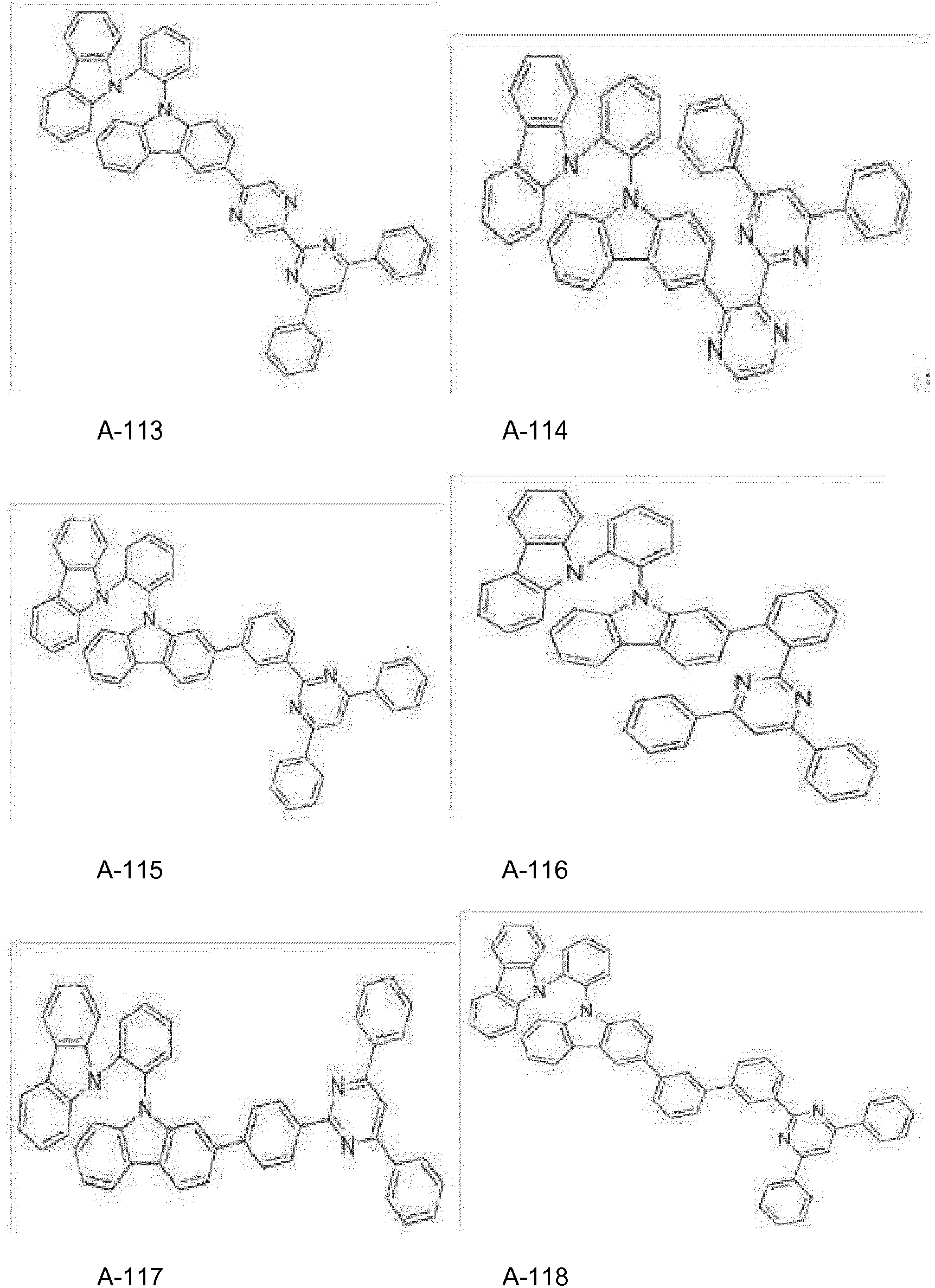


- According to the embodiment, the compound includes a functional group having the desired electron attracting or withdrawing properties when both the electron and the hole properties are required, and thus the compounds may effectively improve the life-span of an organic light emitting diode and decrease a driving voltage thereof.
- The compound for an organic optoelectronic device has a maximum light emitting wavelength in a range of about 320 to about 500 nm and a triplet excited energy (T1) ranging from greater than or equal to about 2.0 eV, and specifically, from about 2.0 to about 4.0 eV, and thus may efficiently transport a host charge having high triplet excited energy to a dopant and increase luminous efficiency of the dopant, and is also freely adjusted regarding HOMO and LUMO energy levels and decreases a driving voltage, and accordingly may be used as a host material or a charge transport material.
- In addition, the compound for an organic optoelectronic device has photoactive and electrical activities, and thus may be used as a nonlinear optic material, an electrode material, a discolored material, or used in a light switch, a sensor, a module, a wave guide, an organic transistor, a laser, a light absorbent, a dielectric material, a separating membrane, and the like.
- The compound for an organic optoelectronic device including the above compounds has a glass transition temperature of greater than or equal to 90 °C, 100 °C, or 110 °C and a thermal decomposition temperature of greater than or equal to 400 °C, 420 °C, or 450 °C indicating improved thermal stability. Thereby, it is possible to produce an organic optoelectronic device having high efficiency.
- The compound for an organic optoelectronic device including the above compounds may play a role of emitting light or injecting and/or transporting electrons, and may also act as a light emitting host with an appropriate dopant. In other words, the compound for an organic optoelectronic device may be used as a phosphorescent or fluorescent host material, a blue light emitting dopant material, or an electron transport material.
- Since the compound for an organic optoelectronic device according to an embodiment is used for an organic thin layer, it may improve the life-span characteristic, efficiency characteristic, electrochemical stability, and thermal stability of an organic photoelectric device, and decrease the driving voltage.
- Further, according to another embodiment, an organic optoelectronic device that includes the compound for an organic optoelectronic device is provided. The organic optoelectronic device may include an organic photoelectric device, an organic light emitting diode, an organic solar cell, an organic transistor, an organic photoconductor drum, an organic memory device, and the like. For example, the compound for an organic optoelectronic device according to an embodiment may be included in an electrode or an electrode buffer layer in an organic solar cell to improve the quantum efficiency, and it may be used as an electrode material for a gate, a source-drain electrode, or the like in an organic transistor.
- Hereinafter, an organic light emitting diode is described.
- According to another embodiment, an organic light emitting diode includes an anode, a cathode, and at least one organic thin layer between the anode and the cathode. The at least one organic thin layer may include the compound for an organic optoelectronic device according to an embodiment of the present disclosure.
- The organic thin layer may include a layer selected from an emission layer, a hole transport layer (HTL), a hole injection layer (HIL), an electron transport layer (ETL), an electron injection layer (EIL), a hole blocking layer, and a combination thereof, wherein at least one of these layers includes the compound for an organic optoelectronic device. Particularly, the compound for an organic optoelectronic device may be included in a hole transport layer (HTL) or a hole injection layer (HIL). In addition, when the compound for an organic optoelectronic device is included in the emission layer, the compound for an organic optoelectronic device may be included as a phosphorescent or fluorescent host, and particularly, as a fluorescent blue dopant material.
-
FIGS. 1 to 5 are cross-sectional views showing exemplary embodiments of organic light emitting diodes including the exemplary embodiment of the compound for an organic optoelectronic device. - Referring to
FIGS. 1 to 5 , organiclight emitting diodes thin layer 105 interposed between ananode 120 and acathode 110. - The
anode 120 includes an anode material, which can help injecting the holes into the organic thin layer. The anode material includes: a metal such as nickel, platinum, vanadium, chromium, copper, zinc, and gold, or alloys thereof; a metal oxide such as zinc oxide, indium oxide, indium tin oxide (ITO), and indium zinc oxide (IZO); a combination of a metal and oxide such as ZnO:Al and SnO2:Sb; or a conductive polymer such as poly(3-methylthiophene), poly[3,4-(ethylene-1,2-dioxy)thiophene] (PEDT), polypyrrole, and polyaniline, but is not limited thereto. In one embodiment, it is preferable to include a transparent electrode including indium tin oxide (ITO) as an anode. - The
cathode 110 includes a cathode material, which can help injecting electrons into the organic thin layer. The cathode material includes: a metal such as magnesium, calcium, sodium, potassium, titanium, indium, yttrium, lithium, gadolinium, aluminum, silver, tin, and lead, or alloys thereof; or a multi-layered material such as LiF/Al, Liq/Al, LiO2/Al, LiF/Ca, LiF/Al, and BaF2/Ca, but is not limited thereto. In one embodiment, it is preferable to include a metal electrode including aluminum as a cathode. - Referring to
FIG. 1 , the organiclight emitting diode 100 includes an organicthin layer 105 including only anemission layer 130. - Referring to
FIG. 2 , a double-layered organiclight emitting diode 200 includes an organicthin layer 105 including anemission layer 230 including an electron transport layer (ETL) (not shown), and a hole transport layer (HTL) 140. As shown inFIG. 2 , the organicthin layer 105 includes a double layer of theemission layer 230 and the hole transport layer (HTL) 140. Theemission layer 230 also functions as an electron transport layer (ETL), and the hole transport layer (HTL) 140 layer has an excellent binding property with a transparent electrode such as ITO or an excellent hole transport capability. - Referring to
FIG. 3 , a three-layered organiclight emitting diode 300 includes an organicthin layer 105 including an electron transport layer (ETL) 150, anemission layer 130, and a hole transport layer (HTL) 140. Theemission layer 130 is independently installed, and layers having an excellent electron transport capability or an excellent hole transport capability are separately stacked. - As shown in
FIG. 4 , a four-layered organiclight emitting diode 400 includes an organicthin layer 105 including an electron injection layer (EIL) 160, anemission layer 130, a hole transport layer (HTL) 140, and a hole injection layer (HIL) 170 for adherence with the anode of ITO. - As shown in
FIG. 5 , a five-layered organiclight emitting diode 500 includes an organicthin layer 105 including an electron transport layer (ETL) 150, anemission layer 130, a hole transport layer (HTL) 140, and a hole injection layer (HIL) 170, and further includes an electron injection layer (EIL) 160 to achieve a low voltage. - In
FIGS. 1 to 5 , the organicthin layer 105 including at least one selected from an electron transport layer (ETL) 150, an electron injection layer (EIL) 160, emission layers 130 and 230, a hole transport layer (HTL) 140, a hole injection layer (HIL) 170, wherein the organic thin layer includes a compound for an organic optoelectronic device. The compound for an organic optoelectronic device may be used for an electron transport layer (ETL) 150 or electron injection layer (EIL) 160. When it is used for the electron transport layer (ETL), it is possible to provide an organic light emitting diode having a simpler structure because it does not require an additional hole blocking layer (not shown). - Furthermore, when the compound for an organic photoelectric device is included in the emission layers 130 and 230, the material for the organic photoelectric device may be included as a phosphorescent or fluorescent host or a fluorescent blue dopant.
- The organic light emitting diode may be fabricated by: forming an anode on a substrate; forming an organic thin layer in accordance with a dry coating method such as evaporation, sputtering, plasma plating, and ion plating, or a wet coating method such as spin coating, dipping, and flow coating; and providing a cathode thereon.
- Another embodiment of the present disclosure provides a display device including the organic photoelectric device according to the above embodiment.
- Hereinafter, the embodiments are illustrated in more detail with reference to examples. These examples, however, should not in any sense be interpreted as limiting the scope of the present disclosure.
- Preparation of Compound for Organic Optoelectronic Device
- The compound A-1 as a specific example of a compound for an organic optoelectronic device according to the present disclosure is synthesized according to the following Reaction Scheme 1.

- 5.00 g (12.9 mmol) of 2-(3-bromophenyl)-4,6-diphenylpyrimidine, 3.94 g (15.5 mmol) of bis(pinacolato)diboron, 527 mg (0.645 mmol) of PdCl2(dppf)·CH2Cl2, and 3.80 g (38.7 mmol) of potassium acetate are added to 100 mL of DMF, and the mixture is heated and agitated at 100 °C. When the reaction is complete, the agitated reaction product is cooled down to room temperature, filtered by passing through silica gel, and then concentrated under a reduced pressure. The product is recrystallized and purified under an ethyl acetate/toluene condition, obtaining 4.59 g of desired intermediate product (A) (a yield of 82 %).
- 1H-NMR (300MHz, CDCl3)(AVANCE DIGITAL 300 (Bruker Co.)): 9.09 (s, 1 H); 8.82 (dt, 1 H); 8.31-8.28 (m, 4H); 8.00 (s, 1 H), 7.97 (dt, 1 H); 7.60-7.50 (m, 7H); 1.99 (s, 12H)
- 1.80 g (4.14 mmol) of the intermediate A, 1.02 g (4.14 mmol) of 3-bromocarbazole, 478 mg (0.414 mmol) of tetrakis(triphenylphosphine)palladium(0) (Pd(PPh3)4), and 1.72 g (12.4 mmol) of potassium carbonate are added to a mixed solution of 8 mL of toluene, 8 mL of tetrahydrofuran, and 8 mL of water. The mixture is refluxed and agitated. When the reaction is complete, the resulting product is cooled down to room temperature and then left. After separating into an aqueous solution layer and an organic solution layer, the aqueous solution layer is removed and the organic solution layer is filtered by passing through silica gel, and then concentrated under a reduced pressure. The obtained product is separated through silica gel column chromatography (ethyl acetate:n-hexane = 1:5 v/v), obtaining 1.43 g of desired intermediate product (B) (a yield of 73 %).
- 1H-NMR (300MHz, CDCl3): 9.04 (s, 1 H); 8.72 (d. 1 H); 8.42 (s, 1 H); 8.33-8.31 (m, 4H); 8.16 (t, 2H); 8.06 (s, 1 H); 7.84-7.81 (m, 2H); 7.66 (d, 1 H); 7.60-7.50 (m, 6H); 7.48-7.44 (m, 2H); 7.27-7.24 (m, 2H)
- 2.00 g (12.0 mmol) of carbazole, 2.02 mL (15.8 mmol) of 1-bromo-3-iodobenzene, 2.29 g (36.0 mmol) of copper (Cu), and 4.98 g (36.0 mmol) of calcium carbonate are added to 30 mL of DMF. The mixture is heated and agitated at 130 °C. When the reaction is complete, the agitated mixture is cooled down to room temperature, diluted with ethyl acetate, filtered by passing through silica gel, and then concentrated under a reduced pressure. The product is separated through silica gel column chromatography (ethyl acetate:n-hexane = 1:20 v/v), obtaining 3.80 g of desired intermediate product (C) (a yield of 98 %).
- 1H-NMR (300MHz, CDCl3): 8.16-8.13 (d, 1 H), 7.75-7.69 (m, 2H), 7.57-7.40 (m, 7H), 7.33-7.30 (m, 2H)
- 474 mg (1.00 mmol) of the intermediate (B), 387 mg (1.20 mmol) of the intermediate (C), 91.6 mg (0.10 mmol) of Pd2(dba)3, 100 µL (0.20 mmol) of tri-tert-butylphosphine (ttbp) (50 % in toluene), and 192 mg (2.00 mmol) of sodium tert-butoxide are added to 10 mL of xylene. The mixture is heated and agitated at 145 °C. When the reaction is complete, the agitated mixture is cooled down to room temperature and filtered by passing through silica gel, and then concentrated under a reduced pressure. The obtained product is separated through silica gel column chromatography (ethyl acetate:n-hexane = 1:4 v/v). The separated product is recrystallized and purified under a toluene/methanol condition, obtaining 465 mg of a desired compound represented by Chemical Formula A-01 (a yield of 65 %).
- 1H-NMR (300MHz, CDCl3): 9.05 (t, 1 H); 8.73 (dt, 1 H); 8.50 (d, 1 H); 8.34-8.30 (m, 4H); 8.23 (d, 1 H); 8.17 (d. 2H); 8.06 (s, 1 H); 7.88-7.83 (m, 4H); 7.77-7.72 (m, 2H); 7.69-7.63 (m, 2H); 7.61-7.52 (m, 8H); 7.50-7.43 (m, 3H); 7.33 (dd, 3H); 7.17 (d, 1 H)
- The compound A-2 as a specific example of a compound for an organic optoelectronic device according to the present disclosure is synthesized according to the following Reaction Scheme 2.
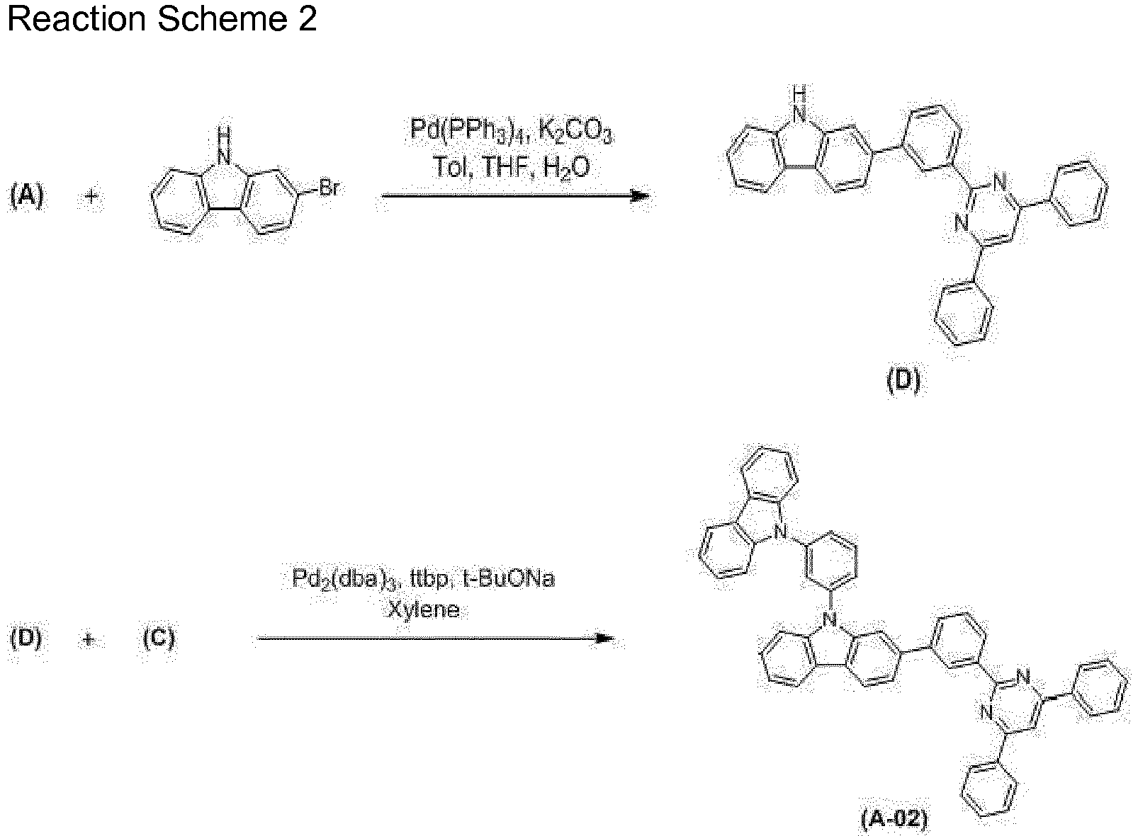
- 1.80 g (4.14 mmol) of the intermediate A, 1.02 g (4.14 mmol) of 2-bromocarbazole, 478 mg (0.414 mmol) of tetrakis(triphenylphosphine)palladium(0) (Pd(PPh3)4), and 1.72 g (12.4 mmol) of potassium carbonate are added to a mixed solution of 8 mL of toluene, 8 mL of tetrahydrofuran, and 8 mL of water. The mixture is refluxed and agitated. When the reaction is complete, the agitated mixture is cooled down to room temperature and then left. After separating into an aqueous solution layer and an organic solution layer, the aqueous solution layer is removed and the organic solution layer is filtered by passing through silica gel, and then concentrated under a reduced pressure. The resulting product is separated through silica gel column chromatography (ethyl acetate:n-hexane = 1:5 v/v), obtaining 1.52 g of desired intermediate product (D) (a yield of 78 %).
- 474 mg (1.00 mmol) of the intermediate (D), 387 mg (1.20 mmol) of the intermediate (C), 91.6 mg (0.10 mmol) of Pd2(dba)3, 100 µL (0.20 mmol) of tri-tert-butylphosphine (ttbp) (50 % in toluene), and 192 mg (2.00 mmol) of sodium tert-butoxide are added to 10 mL of xylene. The mixture is heated and agitated at 145 °C. When the reaction is complete, the agitated mixture is cooled down to room temperature, filtered by passing through silica gel, and then concentrated under a reduced pressure. The resulting product is separated through silica gel column chromatography (ethyl acetate:n-hexane = 1:4 v/v). The obtained product is recrystallized and purified under a toluene/methanol condition, obtaining 515 mg of a desired compound represented by Chemical Formula A-2 (a yield of 72 %).
- The compound A-3 as a specific example of a compound for an organic optoelectronic device according to the present disclosure is synthesized according to the following Reaction Scheme 3.
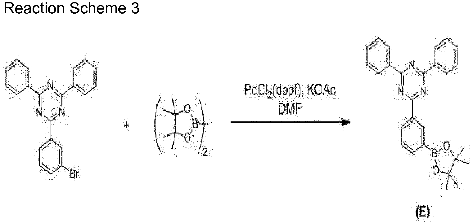

- 5.00 g (12.9 mmol) of 2-(3-bromophenyl)-4,6-diphenyl-1,3,5-triazine), 3.94 g (15.5 mmol) of bis(pinacolato)diboron, 527 mg (0.645 mmol) of PdCl2(dppf)·CH2Cl2, and 3.80 g (38.7 mmol) of potassium acetate are added to 100 mL of DMF. The mixture is heated and agitated at 100 °C. When the reaction is complete, the agitated mixture is cooled down to room temperature and filtered by passing through silica gel, and then concentrated under a reduced pressure. The product is recrystallized and purified under an ethyl acetate/toluene condition, obtaining 4.25 g of desired intermediate product (E) (a yield of 76 %).
- 2.00 g (4.59 mmol) of the intermediate (E), 1.13 g (4.59 mmol) of 3-bromocarbazole, 530 mg (0.459 mmol) of tetrakis(triphenylphosphine)palladium(0) (Pd(PPh3)4), and 1.91 g (13.8 mmol) of potassium carbonate are added to a mixed solution of 10 mL of toluene, 10 mL of tetrahydrofuran, and 10 mL of water, and the mixture is refluxed and agitated. When the reaction is complete, the agitated mixture is cooled down to room temperature and left. After separating into an aqueous solution layer and an organic solution layer, the aqueous solution layer is removed and the organic solution layer is filtered by passing through silica gel, and then concentrated under a reduced pressure. The product is separated through silica gel column chromatography (ethyl acetate:n-hexane = 1:4 <v/v>), obtaining 1.50 g of desired intermediate product (F) (a yield of 69 %).
- 475 mg (1.00 mmol) of the intermediate (F), 387 mg (1.20 mmol) of the intermediate (C), 91.6 mg (0.100 mmol) of Pd2(dba)3, 100 µL (0.20 mmol) of tri-tert-butylphosphine (ttbp) (50 % in toluene), and 192 mg (2.00 mmol) of sodium tert-butoxide are added to 10 mL of xylene. The mixture is heated and agitated at 145 °C. When the reaction is complete, the agitated mixture is cooled down to room temperature and filtered by passing through silica gel, and then concentrated under a reduced pressure. The product is separated through silica gel column chromatography (ethyl acetate:n-hexane = 1:3 <v/v>). The separated product is recrystallized and purified under a toluene/methanol condition, obtaining 422 mg of a desired compound represented by Chemical Formula A-3 (a yield of 59 %).
- The compound A-4 as a specific compound for an organic optoelectronic device according to the present disclosure is synthesized according to the following Reaction Scheme 4.


- 2.00 g (10.2 mmol) of acridone, 1.95 mL (15.3 mmol) of 1-bromo-3-iodobenzene, 1.06 mL (5.10 mmol) of dipivaloylmethane, 389 mg (2.04 mmol) of cuprous iodide (Cul), and 2.82 g (20.4 mmol) of calcium carbonate are added to 50 mL of DMF. The mixture is refluxed and agitated. When the reaction is complete, the agitated mixture is cooled down to room temperature, diluted with ethyl acetate, and filtered by passing through silica gel, and then concentrated under a reduced pressure. The product is separated through silica gel column chromatography (ethyl acetate:n-hexane = 1:10 <v/v>), obtaining 2.85 g of desired intermediate product (G) (a yield of 80 %).
- 474 mg (1.00 mmol) of the intermediate (B), 420 mg (1.20 mmol) of the intermediate (G), 91.6 mg (0.10 mmol) of Pd2(dba)3, 100 µL (0.20 mmol) of tri-tert-butylphosphine (ttbp) (50 % in toluene), and 192 mg (2.00 mmol) of sodium tert-butoxide are added to 10 mL of xylene, and the mixture is heated and agitated at 145 °C. When the reaction is complete, the agitated mixture is cooled down to room temperature, filtered by passing through silica gel, and then concentrated under a reduced pressure. The obtained product is separated through silica gel column chromatography (ethyl acetate:n-hexane = 1:3 <v/v>). The separated product is recrystallized and purified under a toluene/methanol condition, obtaining 387 mg of a compound represented by Chemical Formula A-4 (a yield of 52 %).
- The compound A-5 as specific example of a compound for an organic optoelectronic device is synthesized according to the following Reaction Scheme 5.

- 2.00 g (10.9 mmol) of phenoxazine, 2.08 mL (16.4 mmol) of 1-bromo-3-iodobenzene, 2.08 g (32.7 mmol) of copper (Cu), and 4.52 g (32.7 mmol) of calcium carbonate are added to 30 mL of DMF, and the mixture is heated and agitated at 130 °C. When the reaction is complete, the agitated mixture is cooled down to room temperature, diluted with ethyl acetate, and filtered by passing through silica gel, and then concentrated under a reduced pressure. The obtained product is separated through silica gel column chromatography (ethyl acetate:n-hexane = 1:20 <v/v>), obtaining 1.52 g of a desired compound, an intermediate product (H) (a yield of 41 %).
- <1H-NMR (300MHz, CDCl3): 7.62 (ddd, 1 H); 7.53 (t, 1 H); 7.47 (t, 1 H); 7.31 (ddd, 1 H); 6.71-6.58 (m, 8H); 5.92 (dd, 2H)>
- 474 mg (1.00 mmol) of the intermediate (B), 406 mg (1.20 mmol) of the intermediate (H), 91.6 mg (0.10 mmol) of Pd2(dba)3, 100 µL of (0.20 mmol) of tri-tert-butylphosphine (ttbp) (50 % in toluene), and 192 mg (2.00 mmol) of sodium tert-butoxide are added to 10 mL of xylene, and the mixture is heated and agitated at 145 °C. When the reaction is complete, the agitated mixture is cooled down to room temperature, filtered by passing through silica gel, and then concentrated under a reduced pressure. The obtained product is separated through silica gel column chromatography (ethyl acetate:n-hexane = 1:5 <v/v>). The separated product is recrystallized and purified under a toluene/methanol condition, obtaining 497 mg of a compound represented by Chemical Formula A-5 (a yield of 68 %).
- <1H-NMR (300MHz, CDCl3): 9.04 (t. 1 H); 8.73 (dt, 1 H); 8.48 (d. 1 H); 8.33-8.30 (m, 4H); 8.23 (d, 1 H); 8.05 (s, 1 H); 7.89-7.76 (m, 4H); 7.68-7.65 (m, 2H); 7.63-7.52 (m, 6H); 7.49-7.43 (m, 2H); 7.36-7.31 (m, 1 H); 7.25-7.16 (m, 2H); 6.75-6.67 (m, 6H); 6.17-6.11 (m, 2H)>
- The compound A-6 as a specific compound for an organic optoelectronic device according to the present disclosure is synthesized according to the following Reaction Scheme 6.

- 2.00 g (12.0 mmol) of carbazole, 2.02 mL (15.8 mmol) of 1-bromo-3-iodobenzene, 2.29 g (36.0 mmol) of copper (Cu), and 4.98 g (36.0 mmol) of calcium carbonate are added to 30 mL of DMF, and the mixture is heated and agitated at 130 °C. When the reaction is complete, the agitated mixture is cooled down to room temperature, diluted with ethyl acetate, and filtered by passing through silica gel, and then concentrated under a reduced pressure. The obtained product is separated through silica gel column chromatography (ethyl acetate:n-hexane = 1:20 <v/v>), obtaining 3.68 g of a desired compound, an intermediate product (I) (a yield of 95 %).
- <1H-NMR (300MHz, CDCl3): 8.22 (d, 2H); 7.84-7.76 (m, 2H); 7.55-7.41 (m, 6H); 7.39-7.31 (m, 2H)>
- 474 mg (1.00 mmol) of the intermediate (B), 387 mg (1.20 mmol) of the intermediate (I), 91.6 mg (0.10 mmol) of Pd2(dba)3, 100 µL (0.20 mmol) of tri-tert-butylphosphine (ttbp) (50 % in toluene), and 192 mg (2.00 mmol) of sodium tert-butoxide are added to 10 mL of xylene, and the mixture is heated and agitated at 145 °C. When the reaction is complete, the agitated mixture is cooled down to room temperature, filtered by passing through silica gel, and then concentrated under a reduced pressure. The obtained product is separated through silica gel column chromatography (ethyl acetate:n-hexane = 1:4 <v/v>). The separated product is recrystallized and purified under a toluene/methanol condition, obtaining 386 mg of a compound represented by Chemical Formula A-6 (a yield of 54 %).
- <1H-NMR (300MHz, CDCl3): 9.08 (t. 1 H); 8.74 (dt, 1 H); 8.53 (d, 1 H); 8.34-8.31 (m, 4H); 8.27 (d, 1 H); 8.17 (d, 2H); 8.06 (s, 1 H); 7.91-7.81 (m, 6H); 7.69 (d, 2H); 7.65-7.53 (m, 8H); 7.49-7.46 (m, 3H); 7.40-7.32 (m, 3H); 7.20 (dd, 1H)>
- The compound A-7 as a specific compound for an organic optoelectronic device according to the present disclosure is synthesized according to the following Reaction Scheme 7.


- 5.00 g (12.9 mmol) of 2-(4-bromophenyl)-4,6-diphenylpyrimidine), 3.94 g (15.5 mmol) of bis(pinacolato)diboron, 527 mg (0.645 mmol) of PdCl2(dppf)·CH2Cl2, and 3.80 g (38.7 mmol) of potassium acetate are added to 100 mL of DMF, and the mixture is heated and agitated at 100 °C. When the reaction is complete, the agitated mixture is cooled down to room temperature, filtered by passing through silica gel, and then concentrated under a reduced pressure. The obtained product is recrystallized and purified under an ethyl acetate/toluene condition, obtaining 4.81 g of a desired compound, an intermediate product (J) (a yield of 86 %).
- 1.80 g (4.14 mmol) of the intermediate (J), 1.02 g (4.14 mmol) of 3-bromocarbazole, 478 mg (0.414 mmol) of tetrakis(triphenylphosphine)palladium(0) (Pd(PPh3)4), and 1.72 g (12.4 mmol) of potassium carbonate are added to a mixed solution of 8 mL of toluene, 8 mL of tetrahydrofuran, and 8 mL of water, and the mixture is refluxed and agitated. When the reaction is complete, the agitated mixture is cooled down to room temperature and left. After separating into an aqueous solution layer and an organic solution layer, the aqueous solution layer is removed and the organic solution layer is filtered by passing through silica gel, and then concentrated under a reduced pressure. The obtained product is separated through silica gel column chromatography (ethyl acetate:n-hexane = 1:5 <v/v>), obtaining 1.12 g of a desired compound, an intermediate (K) (a yield of 57 %).
- 474 mg (1.00 mmol) of the intermediate (K), 387 mg (1.20 mmol) of the intermediate (I), 91.6 mg (0.10 mmol) of Pd2(dba)3, 100 µL (0.20 mmol) of tri-tert-butylphosphine (ttbp) (50 % in toluene), and 192 mg (2.00 mmol) of sodium tert-butoxide are added to 10 mL of xylene, and the mixture is heated and agitated at 145 °C. When the reaction is complete, the agitated mixture is cooled down to room temperature, filtered by passing through silica gel, and then concentrated under a reduced pressure. The obtained product is separated through silica gel column chromatography (ethyl acetate:n-hexane = 1:4 <v/v>). The separated product is recrystallized and purified under a toluene/methanol condition, obtaining 444 mg of a desired compound represented by Chemical Formula A-7 (a yield of 62 %).
- The compound A-8 as a specific example of a compound for an organic optoelectronic device according to the present disclosure is synthesized according to the following Reaction Scheme 8.

- 474 mg (1.00 mmol) of the intermediate (K), 387 mg (1.20 mmol) of the intermediate (C), 91.6 mg (0.10 mmol) of Pd2(dba)3, 100 µL (0.20 mmol) of tri-tert-butylphosphine (ttbp) (50 % in toluene), and 192 mg (2.00 mmol) of sodium tert-butoxide are added to 10 mL of xylene, and the mixture is heated and agitated at 145 °C. When the reaction is complete, the agitated mixture is cooled down to room temperature, filtered by passing through silica gel, and then concentrated under a reduced pressure. The obtained product is passed through silica gel column chromatography (ethyl acetate:n-hexane = 1:4 <v/v>). The separated product is recrystallized and purified under a toluene/methanol condition, obtaining 559 mg of a desired compound represented by Chemical Formula A-8 (a yield of 78 %).
- 1H-NMR (300MHz, CDCl3): 8.54 (d, 2H); 8.46 (d, 1 H); 8.34-8.30 (m, 4H); 8.24 (d, 1 H); 8.16 (d, 2H); 8.02 (s, 1 H); 7.91-7.85 (m, 4H); 7.80 (dd, 1 H); 7.72-7.69 (m, 2H); 7.60 (d, 1 H); 7.59-7.53 (m, 8H); 7.49-7.40 (m, 3H); 7.37-7.28 (m, 3H); 7.25-7.16 (m, 1 H)
- Manufacture of Organic Light Emitting Diode
- The host compound synthesized according to Example 1 is doped with 10 wt% of Ir(ppy)3, preparing a mixture for an emission layer. Then, 1 wt% of the mixture for an emission layer is dissolved in a toluene solvent, preparing a composition for an organic photoelectric device.
- First, a transparent electrode substrate is fabricated by coating ITO (indiumtin oxide) on a glass substrate, cleaning it, patterning the ITO using a photosensitive resin and an etchant, and cleaning it again. Next, PEDOT (Batron P 4083, Bayer Inc.) is coated to be about 55 nm thick on the ITO and fired at 180 °C for about one hour, forming a hole injection layer (HIL). Then, the composition for an organic photoelectric device prepared in the first step is spin-coated on the hole injection layer (HIL) and fired in a vacuum oven to completely remove a solvent and form an emission layer. Herein, the composition for an emission layer is filtered through a 0.2 mm filter before the spin-coating. The emission layer is formed to be about 45 nm thick by controlling the concentration and spin-coating speed of the composition. Then, an electron transport layer (ETL) is formed by respectively vacuum-depositing ET202 and LiQ to be 15 nm thick on the emission layer with a vacuum depositor, while a vacuum degree of less than or equal to 4 X 10⁻⁶ Torr is maintained. Next, Al is sequentially deposited to be 120 nm thick to form a negative electrode on the electron transport layer (ETL). In the deposition, the thickness and speed of the negative electrode are controlled using a crystal sensor.
- The organic light emitting diode is specifically fabricated to have a structure of ITO / PEDOT:PSS (55 nm) / EML (host compound (90 wt%) + dopant compound (10 wt%), 45 nm) / ET202 (15 nm) / LiQ (15 nm) / Al (120 nm).
- An organic light emitting diode is fabricated according to the same method as Example 9, except for using the host compound synthesized according to Example 2 instead of the one according to Example 1.
- An organic light emitting diode is fabricated according to the same method as Example 9, except for using the host compound synthesized according to Example 3 instead of the one according to Example 1.
- An organic light emitting diode is fabricated according to the same method as Example 9, except for using the host compound synthesized according to Example 4 instead of the one according to Example 1.
- An organic light emitting diode is fabricated according to the same method as Example 9, except for using the host compound synthesized according to Example 5 instead of the one according to Example 1.
- An organic light emitting diode is fabricated according to the same method as Example 9, except for using the host compound synthesized according to Example 6 instead of the one according to Example 1.
- An organic light emitting diode is fabricated according to the same method as Example 9, except for using the host compound synthesized according to Example 7 instead of the one according to Example 1.
- An organic light emitting diode is fabricated according to the same method as Example 9, except for using the host compound synthesized according to Example 8 instead of the one according to Example 1.
- An organic light emitting diode is fabricated according to the same method as Example 9, except for using a mixture of PVK (polyvinylcarbazole) and PBD (2-(4-biphenyl)-5-(4-t-butylphenyl)-1,3,4-oxadiazole) represented by the following chemical formulae in a weight ratio of 1:1 as a host instead of the host compound synthesized according to Example 1.
- The Ir(ppy)3, PVK, and PBD used to fabricate the organic light emitting diode have the following structures.

- Performance Measurement of Organic Light Emitting Diode
- Each organic light emitting diode according to Examples 9 to 16 and Comparative Example 1 is measured regarding current density change depending upon the voltage, luminance change, and luminous efficiency. The results are shown in the Table 1. The specific methods are as follows.
- The obtained organic light emitting diodes are measured regarding current value flowing in a unit device, while their voltages are increased from 0 V to 10 V using a current-voltage meter (Keithley 2400). The measured current value is divided by an area to calculate current density.
- The organic light emitting diodes are measured regarding luminance using a luminance meter (Minolta Cs-1000A) while their voltages are increased from 0 V to 10 V.
- Current efficiency (cd/A) and electric power efficiency (Im/W) at the same luminance (1000 cd/m2) are calculated by using luminance and current density from (1) and (2) and a voltage.
Table 1 Results at 1000 cd/m2 Driving voltage (V) Current efficiency (cd/A) Electric power efficiency (Im/W) EL color Example 9 5.7 18.6 10.2 Green Example 10 5.5 17.8 10.2 Green Example 11 5.2 20.5 12.4 Green Example 12 5.2 19.4 11.7 Green Example 13 5.5 15.6 8.9 Green Example 14 4.9 27.3 17.5 Green Example 15 4.8 25.0 16.4 Green Example 16 5.6 16.7 9.4 Green Comparative Example 1 5.1 13.2 8.1 Green - Referring to the results in Table 1, the host materials used in Examples 9 to 16 have excellent device performance in terms of luminous efficiency and electric power efficiency compared with the one used in Comparative Example 1. Specifically, the host materials used in Example 14 and 15 have excellent device performance in terms of driving voltage, current efficiency, and electric power efficiency compared with the one according to Comparative Example 1. Accordingly, the host materials may realize an organic light emitting diode having a low voltage, high efficiency, high luminance, and a long life-span.
- While this application has been described in connection with what is presently considered to be practical exemplary embodiments, it is to be understood that the application is not limited to the disclosed embodiments, but, on the contrary, is intended to cover various modifications and equivalent arrangements included within the scope of the appended claims. Therefore, the aforementioned embodiments should be understood to be exemplary but not limiting the present invention in any way.
Claims (15)
- A compound for an organic optoelectronic device represented by Chemical Formula 1:
 X1 to X3 are independently -C(R')- or -N-, provided that at least one of X1 to X3 is -N-,X4 is a single bond, -C(R')(R")-, -O-, -S-, -S(=O)-, -S(=O)2-, -Si(R')(R")- or - C(=O)-,R1 to R4, R', and R" are independently hydrogen, deuterium, a halogen, a cyano group, a hydroxyl group, an amino group, a substituted or unsubstituted C1 to C20 amine group, a nitro group, a carboxyl group, a ferrocenyl group, a substituted or unsubstituted C1 to C20 alkyl group, a substituted or unsubstituted C6 to C30 aryl group, a substituted or unsubstituted C2 to C30 heteroaryl group, a substituted or unsubstituted C1 to C20 alkoxy group, a substituted or unsubstituted C6 to C20 aryloxy group, a substituted or unsubstituted C3 to C40 silyloxy group, a substituted or unsubstituted C1 to C20 acyl group, a substituted or unsubstituted C2 to C20 alkoxycarbonyl group, a substituted or unsubstituted C2 to C20 acyloxy group, a substituted or unsubstituted C2 to C20 acylamino group, a substituted or unsubstituted C2 to C20 alkoxycarbonylamino group, a substituted or unsubstituted C7 to C20 aryloxycarbonylamino group, a substituted or unsubstituted C1 to C20 sulfamoylamino group, a substituted or unsubstituted C1 to C20 sulfonyl group, a substituted or unsubstituted C1 to C20 alkylthiol group, a substituted or unsubstituted C6 to C20 arylthiol group, a substituted or unsubstituted C1 to C20 heterocyclothiol group, a substituted or unsubstituted C1 to C20 ureide group, a substituted or unsubstituted C3 to C40 silyl group, or a combination thereof,L is a substituted or unsubstituted C2 to C20 alkenylene group, a substituted or unsubstituted C2 to C20 alkynylene group, a substituted or unsubstituted C6 to C30 arylene group, a substituted or unsubstituted C2 to C30 heteroarylene group, or combination thereof, andAr1 and Ar2 are independently a substituted or unsubstituted C6 to C30 aryl group or a substituted or unsubstituted C2 to C30 heteroaryl group.
 - The compound for an organic optoelectronic device of claim 1, wherein the compound for an organic optoelectronic device is represented by Chemical Formula 2:

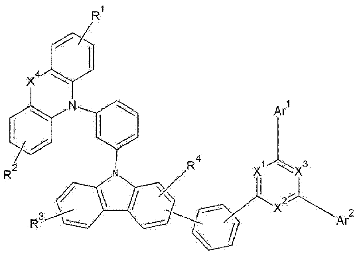 X1 to X3 are independently -C(R')- or -N-, provided that at least one of X1 to X3 is -N-,X4 is a single bond, -C(R')(R")-, -O-, -S-, -S(=O)-, -S(=O)2-, -Si(R')(R")- or - C(=O)-,R1 to R4, R', and R" are independently hydrogen, deuterium, a halogen, a cyano group, a hydroxyl group, an amino group, a substituted or unsubstituted C1 to C20 amine group, a nitro group, a carboxyl group, a ferrocenyl group, a substituted or unsubstituted C1 to C20 alkyl group, a substituted or unsubstituted C6 to C30 aryl group, a substituted or unsubstituted C2 to C30 heteroaryl group, a substituted or unsubstituted C1 to C20 alkoxy group, a substituted or unsubstituted C6 to C20 aryloxy group, a substituted or unsubstituted C3 to C40 silyloxy group, a substituted or unsubstituted C1 to C20 acyl group, a substituted or unsubstituted C2 to C20 alkoxycarbonyl group, a substituted or unsubstituted C2 to C20 acyloxy group, a substituted or unsubstituted C2 to C20 acylamino group, a substituted or unsubstituted C2 to C20 alkoxycarbonylamino group, a substituted or unsubstituted C7 to C20 aryloxycarbonylamino group, a substituted or unsubstituted C1 to C20 sulfamoylamino group, a substituted or unsubstituted C1 to C20 sulfonyl group, a substituted or unsubstituted C1 to C20 alkylthiol group, a substituted or unsubstituted C6 to C20 arylthiol group, a substituted or unsubstituted C1 to C20 heterocyclothiol group, a substituted or unsubstituted C1 to C20 ureide group, a substituted or unsubstituted C3 to C40 silyl group, or a combination thereof, andAr1 and Ar2 are independently a substituted or unsubstituted C6 to C30 aryl group or a substituted or unsubstituted C2 to C30 heteroaryl group.
 - The compound for an organic optoelectronic device of claim 1, wherein the compound for an organic optoelectronic device is represented by Chemical Formula 3:
 X1 to X3 are independently -C(R')- or -N-, provided that at least one of X1 to X3 is -N-,X4 is a single bond, -C(R')(R")-, -O-, -S-, -S(=O)-, -S(=O)2-, -Si(R')(R")- or - C(=O)-,R1 to R4, R', and R" are independently hydrogen, deuterium, a halogen, a cyano group, a hydroxyl group, an amino group, a substituted or unsubstituted C1 to C20 amine group, a nitro group, a carboxyl group, a ferrocenyl group, a substituted or unsubstituted C1 to C20 alkyl group, a substituted or unsubstituted C6 to C30 aryl group, a substituted or unsubstituted C2 to C30 heteroaryl group, a substituted or unsubstituted C1 to C20 alkoxy group, a substituted or unsubstituted C6 to C20 aryloxy group, a substituted or unsubstituted C3 to C40 silyloxy group, a substituted or unsubstituted C1 to C20 acyl group, a substituted or unsubstituted C2 to C20 alkoxycarbonyl group, a substituted or unsubstituted C2 to C20 acyloxy group, a substituted or unsubstituted C2 to C20 acylamino group, a substituted or unsubstituted C2 to C20 alkoxycarbonylamino group, a substituted or unsubstituted C7 to C20 aryloxycarbonylamino group, a substituted or unsubstituted C1 to C20 sulfamoylamino group, a substituted or unsubstituted C1 to C20 sulfonyl group, a substituted or unsubstituted C1 to C20 alkylthiol group, a substituted or unsubstituted C6 to C20 arylthiol group, a substituted or unsubstituted C1 to C20 heterocyclothiol group, a substituted or unsubstituted C1 to C20 ureide group, a substituted or unsubstituted C3 to C40 silyl group, or a combination thereof, andAr1 and Ar2 are independently a substituted or unsubstituted C6 to C30 aryl group or a substituted or unsubstituted C2 to C30 heteroaryl group.
 - The compound for an organic optoelectronic device of claim 1, wherein the compound for an organic optoelectronic device is represented by Chemical Formula 4: Chemical Formula 4
 X1 to X3 are independently -C(R')- or -N-, provided that at least one of X1 to X3 is -N-,X4 is a single bond, -C(R')(R")-, -O-, -S-, -S(=O)-, -S(=O)2-, -Si(R')(R")- or - C(=O)-,R1 to R4, R', and R" are independently hydrogen, deuterium, a halogen, a cyano group, a hydroxyl group, an amino group, a substituted or unsubstituted C1 to C20 amine group, a nitro group, a carboxyl group, a ferrocenyl group, a substituted or unsubstituted C1 to C20 alkyl group, a substituted or unsubstituted C6 to C30 aryl group, a substituted or unsubstituted C2 to C30 heteroaryl group, a substituted or unsubstituted C1 to C20 alkoxy group, a substituted or unsubstituted C6 to C20 aryloxy group, a substituted or unsubstituted C3 to C40 silyloxy group, a substituted or unsubstituted C1 to C20 acyl group, a substituted or unsubstituted C2 to C20 alkoxycarbonyl group, a substituted or unsubstituted C2 to C20 acyloxy group, a substituted or unsubstituted C2 to C20 acylamino group, a substituted or unsubstituted C2 to C20 alkoxycarbonylamino group, a substituted or unsubstituted C7 to C20 aryloxycarbonylamino group, a substituted or unsubstituted C1 to C20 sulfamoylamino group, a substituted or unsubstituted C1 to C20 sulfonyl group, a substituted or unsubstituted C1 to C20 alkylthiol group, a substituted or unsubstituted C6 to C20 arylthiol group, a substituted or unsubstituted C1 to C20 heterocyclothiol group, a substituted or unsubstituted C1 to C20 ureide group, a substituted or unsubstituted C3 to C40 silyl group, or a combination thereof, andAr1 and Ar2 are independently a substituted or unsubstituted C6 to C30 aryl group or a substituted or unsubstituted C2 to C30 heteroaryl group.
 - The compound for an organic optoelectronic device of claim 1, wherein the compound for an organic optoelectronic device is represented by Chemical Formula 5:
 X1 to X3 are independently -C(R')- or -N-, provided that at least one of X1 to X3 is -N-,X4 is a single bond, -C(R')(R")-, -O-, -S-, -S(=O)-, -S(=O)2-, -Si(R')(R")- or - C(=O)-,R1 to R4, R', and R" are independently hydrogen, deuterium, a halogen, a cyano group, a hydroxyl group, an amino group, a substituted or unsubstituted C1 to C20 amine group, a nitro group, a carboxyl group, a ferrocenyl group, a substituted or unsubstituted C1 to C20 alkyl group, a substituted or unsubstituted C6 to C30 aryl group, a substituted or unsubstituted C2 to C30 heteroaryl group, a substituted or unsubstituted C1 to C20 alkoxy group, a substituted or unsubstituted C6 to C20 aryloxy group, a substituted or unsubstituted C3 to C40 silyloxy group, a substituted or unsubstituted C1 to C20 acyl group, a substituted or unsubstituted C2 to C20 alkoxycarbonyl group, a substituted or unsubstituted C2 to C20 acyloxy group, a substituted or unsubstituted C2 to C20 acylamino group, a substituted or unsubstituted C2 to C20 alkoxycarbonylamino group, a substituted or unsubstituted C7 to C20 aryloxycarbonylamino group, a substituted or unsubstituted C1 to C20 sulfamoylamino group, a substituted or unsubstituted C1 to C20 sulfonyl group, a substituted or unsubstituted C1 to C20 alkylthiol group, a substituted or unsubstituted C6 to C20 arylthiol group, a substituted or unsubstituted C1 to C20 heterocyclothiol group, a substituted or unsubstituted C1 to C20 ureide group, a substituted or unsubstituted C3 to C40 silyl group, or a combination thereof, andAr1 and Ar2 are independently a substituted or unsubstituted C6 to C30 aryl group or a substituted or unsubstituted C2 to C30 heteroaryl group.
 - The compound for an organic optoelectronic device of claim 1, wherein the compound for an organic optoelectronic device is represented by Chemical Formula 6:
 X1 to X3 are independently -C(R')- or -N-, provided that at least one of X1 to X3 is -N-,R1 to R4 and R' are independently hydrogen, deuterium, a halogen, a cyano group, a hydroxyl group, an amino group, a substituted or unsubstituted C1 to C20 amine group, a nitro group, a carboxyl group, a ferrocenyl group, a substituted or unsubstituted C1 to C20 alkyl group, a substituted or unsubstituted C6 to C30 aryl group, a substituted or unsubstituted C2 to C30 heteroaryl group, a substituted or unsubstituted C1 to C20 alkoxy group, a substituted or unsubstituted C6 to C20 aryloxy group, a substituted or unsubstituted C3 to C40 silyloxy group, a substituted or unsubstituted C1 to C20 acyl group, a substituted or unsubstituted C2 to C20 alkoxycarbonyl group, a substituted or unsubstituted C2 to C20 acyloxy group, a substituted or unsubstituted C2 to C20 acylamino group, a substituted or unsubstituted C2 to C20 alkoxycarbonylamino group, a substituted or unsubstituted C7 to C20 aryloxycarbonylamino group, a substituted or unsubstituted C1 to C20 sulfamoylamino group, a substituted or unsubstituted C1 to C20 sulfonyl group, a substituted or unsubstituted C1 to C20 alkylthiol group, a substituted or unsubstituted C6 to C20 arylthiol group, a substituted or unsubstituted C1 to C20 heterocyclothiol group, a substituted or unsubstituted C1 to C20 ureide group, a substituted or unsubstituted C3 to C40 silyl group, or a combination thereof, andAr1 and Ar2 are independently a substituted or unsubstituted C6 to C30 aryl group or a substituted or unsubstituted C2 to C30 heteroaryl group.
 - The compound for an organic optoelectronic device of claim 6, wherein the Ar1 and Ar2 are independently a substituted or unsubstituted C6 to C30 aryl group.
- The compound for an organic optoelectronic device of any of claims 1-7, wherein the X1 to X3 are independently -C(R')- or -N- provided that at least two of the X1 to X3 are -N-.
- The compound for an organic optoelectronic device of claim 1, which is represented by at least one of Chemical Formulas A-1 to A-140:
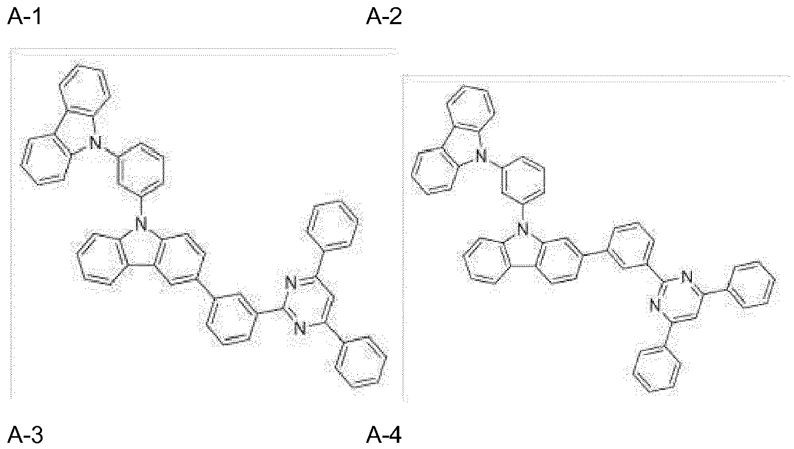


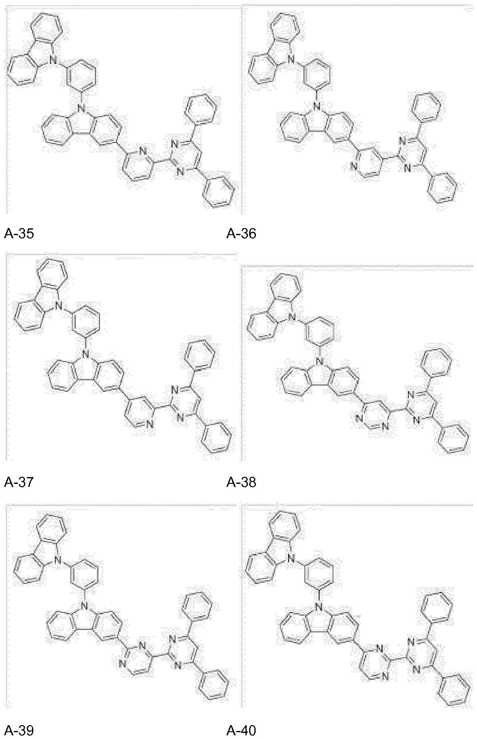


- An organic optoelectronic device comprising the compound of any of claims 1-9.
- The organic optoelectronic device of claim 10, wherein the organic optoelectronic device is selected from an organic photoelectric device, an organic light emitting diode, an organic solar cell, an organic transistor, an organic photoconductor drum, and an organic memory device.
- An organic light emitting diode comprising:an anode, a cathode, and at least one organic thin layer interposed between the anode and cathode,wherein at least one organic thin layer comprises the compound of any of claims 1-9.
- The organic light emitting diode of claim 12, wherein the organic thin layer is selected from an emission layer, a hole transport layer, a hole injection layer, an electron transport layer, an electron injection layer, a hole blocking layer, and a combination thereof.
- The organic light emitting diode of claim 12 or 13, wherein the organic thin layer comprises an emission layer, and wherein the emission layer comprises the compound of claim 1.
- A display device comprising the organic light emitting diode according to any of claims 12-14.
Applications Claiming Priority (1)
| Application Number | Priority Date | Filing Date | Title |
|---|---|---|---|
| KR1020120144602A KR101593182B1 (en) | 2012-12-12 | 2012-12-12 | Compound for organic optoelectronic device, organic light emitting diode including the same and display including the organic light emitting diode |
Publications (3)
| Publication Number | Publication Date |
|---|---|
| EP2743327A2 true EP2743327A2 (en) | 2014-06-18 |
| EP2743327A3 EP2743327A3 (en) | 2014-07-23 |
| EP2743327B1 EP2743327B1 (en) | 2018-01-31 |
Family
ID=49585314
Family Applications (1)
| Application Number | Title | Priority Date | Filing Date |
|---|---|---|---|
| EP13193162.8A Active EP2743327B1 (en) | 2012-12-12 | 2013-11-15 | Compound for organic optoelectronic device, optoelectronic device and organic light emitting diode including the same, and display including the organic light emitting diode |
Country Status (6)
| Country | Link |
|---|---|
| US (1) | US9406891B2 (en) |
| EP (1) | EP2743327B1 (en) |
| JP (1) | JP6523599B2 (en) |
| KR (1) | KR101593182B1 (en) |
| CN (1) | CN103864766B (en) |
| TW (1) | TWI593686B (en) |
Families Citing this family (22)
| Publication number | Priority date | Publication date | Assignee | Title |
|---|---|---|---|---|
| KR101499356B1 (en) | 2013-06-28 | 2015-03-05 | 주식회사 엘지화학 | Hetero-cyclic compound and organic light emitting device comprising the same |
| KR101547065B1 (en) * | 2013-07-29 | 2015-08-25 | 주식회사 엘지화학 | Hetero-cyclic compound and organic light emitting device comprising the same |
| KR102313358B1 (en) * | 2014-07-10 | 2021-10-18 | 삼성디스플레이 주식회사 | Organic light emitting device |
| KR102386839B1 (en) | 2014-12-22 | 2022-04-15 | 삼성전자주식회사 | Organic light-emitting device |
| US10403826B2 (en) | 2015-05-07 | 2019-09-03 | Universal Display Corporation | Organic electroluminescent materials and devices |
| US10043984B2 (en) * | 2015-07-01 | 2018-08-07 | Samsung Electronics Co., Ltd. | Condensed cyclic compound and organic light-emitting device including the same |
| KR102837349B1 (en) * | 2015-07-20 | 2025-07-24 | 듀폰스페셜티머터리얼스코리아 유한회사 | Luminescent Material for Delayed Fluorescence and Organic Electroluminescent Device Comprising the Same |
| KR102486381B1 (en) * | 2015-08-13 | 2023-01-09 | 삼성전자주식회사 | Condensed cyclic compound and organic light emitting device including the same |
| KR102491790B1 (en) * | 2015-09-25 | 2023-01-26 | 엘지디스플레이 주식회사 | Organic Light Emitting Diode Device |
| CN105294663B (en) * | 2015-11-11 | 2019-01-15 | 上海道亦化工科技有限公司 | One kind containing pyridine compounds and its organic electroluminescence device |
| KR102529631B1 (en) * | 2015-11-30 | 2023-05-04 | 삼성전자주식회사 | Organic photoelectronic device and image sensor |
| JP6848424B2 (en) * | 2016-01-15 | 2021-03-24 | 東ソー株式会社 | Carbazole compounds and their uses |
| WO2017122669A1 (en) * | 2016-01-15 | 2017-07-20 | 東ソー株式会社 | Carbazole compound and application thereof |
| KR102633852B1 (en) * | 2016-01-25 | 2024-02-07 | 삼성디스플레이 주식회사 | Carbazole-based compound and organic light emitting device comprising the same |
| KR102451310B1 (en) * | 2017-12-08 | 2022-10-05 | 엘지디스플레이 주식회사 | Organic compounds, organic light emitting diode and organic light emittid device having the compounds |
| CN108101893B (en) * | 2018-01-30 | 2021-01-22 | 烟台九目化学股份有限公司 | Preparation of organic compound taking carbazole and pyrimidine as cores and application of organic compound in OLED |
| CN108929322A (en) * | 2018-08-12 | 2018-12-04 | 瑞声科技(南京)有限公司 | A kind of compound containing azepine carbazole unit and its application |
| EP3689888B1 (en) | 2019-01-31 | 2021-09-22 | Samsung Electronics Co., Ltd. | Organometallic compound and organic light-emitting device including the same |
| KR102896847B1 (en) | 2019-01-31 | 2025-12-05 | 삼성전자주식회사 | Organometallic compound and organic light emitting device including the same |
| TWI710621B (en) * | 2019-07-22 | 2020-11-21 | 昱鐳光電科技股份有限公司 | Naphthyl-substituted phenylpyrimidines compounds and organic electroluminescent devices using the same |
| CN112225686B (en) * | 2020-10-21 | 2022-10-21 | 深圳大学 | Organic compound and electroluminescent device using the same |
| CN114773322A (en) * | 2022-04-13 | 2022-07-22 | 吉林奥来德光电材料股份有限公司 | An organic electroluminescent material and an organic electroluminescent device comprising the same |
Family Cites Families (33)
| Publication number | Priority date | Publication date | Assignee | Title |
|---|---|---|---|---|
| EP1784470B1 (en) | 2004-08-23 | 2013-06-05 | Lg Chem, Ltd. | New luminescent material and organic electroluminescent device using the same |
| KR101388472B1 (en) | 2004-12-10 | 2014-04-23 | 미쓰비시 가가꾸 가부시키가이샤 | Organic compound, charge-transporting material, and organic electroluminescent element |
| US7597967B2 (en) | 2004-12-17 | 2009-10-06 | Eastman Kodak Company | Phosphorescent OLEDs with exciton blocking layer |
| JP4976292B2 (en) | 2005-08-03 | 2012-07-18 | 新日鐵化学株式会社 | Heterocyclic compound and organic electroluminescence device using the same |
| US8242488B2 (en) * | 2007-05-30 | 2012-08-14 | Konica Minolta Holdings, Inc. | Organic electroluminescent element, display device, and illuminating device |
| EP2460866B1 (en) * | 2008-05-13 | 2019-12-11 | Konica Minolta Holdings, Inc. | Organic electroluminescent element, display device and lighting device |
| JP5338184B2 (en) * | 2008-08-06 | 2013-11-13 | コニカミノルタ株式会社 | Organic electroluminescence element, display device, lighting device |
| JP4474493B1 (en) | 2009-07-31 | 2010-06-02 | 富士フイルム株式会社 | Organic electroluminescence device |
| JP4590020B1 (en) | 2009-07-31 | 2010-12-01 | 富士フイルム株式会社 | Charge transport material and organic electroluminescent device |
| JP4523992B1 (en) | 2009-07-31 | 2010-08-11 | 富士フイルム株式会社 | Organic electroluminescence device |
| KR20110014752A (en) | 2009-08-06 | 2011-02-14 | 엘지디스플레이 주식회사 | Red phosphorescent organic light emitting device and its manufacturing method |
| KR101149528B1 (en) | 2009-08-10 | 2012-05-29 | 에스에프씨 주식회사 | Aromatic Compound and organoelectroluminescent device using the same |
| KR101115036B1 (en) | 2009-08-18 | 2012-03-06 | 덕산하이메탈(주) | Compound Containing Thianthrene And Organic Electronic Element Using The Same, Terminal Thereof |
| KR101128048B1 (en) * | 2009-10-15 | 2012-04-02 | 임대순 | Anchor body for a permanent ground anchor |
| KR101233380B1 (en) * | 2009-10-21 | 2013-02-15 | 제일모직주식회사 | Novel compound for organic photoelectric device and organic photoelectric device including the same |
| US8828561B2 (en) | 2009-11-03 | 2014-09-09 | Cheil Industries, Inc. | Compound for organic photoelectric device and organic photoelectric device including the same |
| KR101506999B1 (en) | 2009-11-03 | 2015-03-31 | 제일모직 주식회사 | Compound for organic photoelectric device and organic photoelectric device including the same |
| KR20110066763A (en) | 2009-12-11 | 2011-06-17 | 덕산하이메탈(주) | Compound containing indolo acridine and organic electric device using the same, the terminal |
| JP5722000B2 (en) | 2010-01-15 | 2015-05-20 | ユー・ディー・シー アイルランド リミテッド | Charge transport material and organic electroluminescent device |
| JP5650932B2 (en) | 2010-01-28 | 2015-01-07 | ユー・ディー・シー アイルランド リミテッド | Organic electroluminescent device and charge transport material |
| KR101181277B1 (en) | 2010-03-18 | 2012-09-10 | 덕산하이메탈(주) | Compound Containing Indoloacridine And Organic Electronic Element Using The Same, Terminal Thereof |
| KR101181270B1 (en) | 2010-03-18 | 2012-09-10 | 덕산하이메탈(주) | Compound Containing Indoloacridine And Organic Electronic Element Using The Same, Terminal Thereof |
| JP4729642B1 (en) | 2010-07-09 | 2011-07-20 | 富士フイルム株式会社 | Organic electroluminescence device |
| JP4741028B1 (en) | 2010-07-09 | 2011-08-03 | 富士フイルム株式会社 | Organic electroluminescence device |
| KR20120038056A (en) | 2010-10-13 | 2012-04-23 | 롬엔드하스전자재료코리아유한회사 | Novel compounds for organic electronic material and organic electroluminescent device using the same |
| DE102010048497A1 (en) | 2010-10-14 | 2012-04-19 | Merck Patent Gmbh | Formulations for organic electroluminescent devices |
| KR20130130757A (en) | 2010-11-24 | 2013-12-02 | 메르크 파텐트 게엠베하 | Material for organic electroluminescence device |
| KR101423174B1 (en) * | 2010-12-01 | 2014-07-25 | 제일모직 주식회사 | Compound for organic photoelectric device and organic photoelectric device including the same |
| KR101547410B1 (en) | 2010-12-20 | 2015-08-25 | 이 아이 듀폰 디 네모아 앤드 캄파니 | Compositions for electronic applications |
| KR20120070468A (en) | 2010-12-21 | 2012-06-29 | (주)씨에스엘쏠라 | Organic light compound and organic light device using the same |
| CN103430344B (en) | 2011-03-14 | 2016-03-23 | 东丽株式会社 | Light emitting element material and light-emitting component |
| KR20120122813A (en) | 2011-04-29 | 2012-11-07 | 롬엔드하스전자재료코리아유한회사 | Novel organic electroluminescence compounds and organic electroluminescence device using the same |
| KR20120122812A (en) * | 2011-04-29 | 2012-11-07 | 롬엔드하스전자재료코리아유한회사 | Novel organic electroluminescence compounds and organic electroluminescence device using the same |
-
2012
- 2012-12-12 KR KR1020120144602A patent/KR101593182B1/en active Active
-
2013
- 2013-07-11 US US13/939,811 patent/US9406891B2/en active Active
- 2013-11-15 EP EP13193162.8A patent/EP2743327B1/en active Active
- 2013-11-19 CN CN201310582433.8A patent/CN103864766B/en active Active
- 2013-12-06 JP JP2013252825A patent/JP6523599B2/en active Active
- 2013-12-12 TW TW102145754A patent/TWI593686B/en active
Non-Patent Citations (1)
| Title |
|---|
| None |
Also Published As
| Publication number | Publication date |
|---|---|
| JP2014118410A (en) | 2014-06-30 |
| JP6523599B2 (en) | 2019-06-05 |
| TWI593686B (en) | 2017-08-01 |
| US20140158999A1 (en) | 2014-06-12 |
| EP2743327B1 (en) | 2018-01-31 |
| TW201427973A (en) | 2014-07-16 |
| KR20140076253A (en) | 2014-06-20 |
| KR101593182B1 (en) | 2016-02-19 |
| US9406891B2 (en) | 2016-08-02 |
| CN103864766B (en) | 2017-10-31 |
| EP2743327A3 (en) | 2014-07-23 |
| CN103864766A (en) | 2014-06-18 |
Similar Documents
| Publication | Publication Date | Title |
|---|---|---|
| US9406891B2 (en) | Compound for organic optoelectronic device, organic light emitting diode including the same, and display including the organic light emitting diode | |
| EP2796530B1 (en) | Compound for an organic optoelectronic element, organic light-emitting element comprising same, and display device comprising the organic light-emitting element | |
| US10121973B2 (en) | Compound for organic optoelectronic device, organic light-emitting diode including same, and display device including organic light-emitting diode | |
| EP2842954B1 (en) | Compound for organic optoelectric device, organic light emitting device containing same, and display device containing said organic light emitting device | |
| EP2508585B1 (en) | Compound for organic optoelectronic device, organic light emitting diode including the same, and display device including organic light emitting diode | |
| US20150144937A1 (en) | Compound for organic optoelectronic device, organic light emitting diode comprising same, and display device comprising organic light emitting diode | |
| US20150263294A1 (en) | Compound for organic optoelectronic device, organic light-emitting device including same, and display device including the organic light- emitting diode | |
| EP2796529B1 (en) | Compound for an organic optoelectronic device, organic light-emitting element comprising same, and display device comprising the organic light-emitting element | |
| US9793488B2 (en) | Compound for organic optoelectronic element, organic light-emitting element comprising same, and display device comprising the organic light-emitting element | |
| WO2014104535A1 (en) | Compound for organic optoelectronic device, organic light-emitting diode including same, and display apparatus including said organic light-emitting diode | |
| US20130299794A1 (en) | Compound for organic optoelectronic device, organic light emitting diode including the same and display including the organic light emitting diode | |
| CN104703969A (en) | Fluoranthene compounds and organic electronic devices containing them | |
| EP2520632A2 (en) | Compound for organic photoelectric device and organic photoelectric device including the compound | |
| CN104428283A (en) | Polycyclic compound and organic electronic device comprising same | |
| KR20180062343A (en) | Hetero-cyclic compound and organic light emitting device using the same | |
| KR20140045154A (en) | Compound for organic optoelectronic device, organic light emitting diode including the same and display including the organic light emitting diode | |
| KR101728498B1 (en) | Compound for organic optoelectronic device, organic light emitting diode including the same and display including the organic light emitting diode | |
| KR101969956B1 (en) | Compound for organic optoelectronic device, organic light emitting diode including the same and display including the organic light emitting diode | |
| KR20140087648A (en) | Compound for organic optoelectronic device, organic light emitting diode including the same and display including the organic light emitting diode | |
| KR20140087646A (en) | COMPOUND FOR ORGANIC OPTOELECTRONIC DEVICE, ORGANIC LiGHT EMITTING DIODE INCLUDING THE SAME AND DISPLAY INCLUDING THE ORGANIC LiGHT EMITTING DIODE |
Legal Events
| Date | Code | Title | Description |
|---|---|---|---|
| PUAI | Public reference made under article 153(3) epc to a published international application that has entered the european phase |
Free format text: ORIGINAL CODE: 0009012 |
|
| 17P | Request for examination filed |
Effective date: 20131115 |
|
| AK | Designated contracting states |
Kind code of ref document: A2 Designated state(s): AL AT BE BG CH CY CZ DE DK EE ES FI FR GB GR HR HU IE IS IT LI LT LU LV MC MK MT NL NO PL PT RO RS SE SI SK SM TR |
|
| AX | Request for extension of the european patent |
Extension state: BA ME |
|
| PUAL | Search report despatched |
Free format text: ORIGINAL CODE: 0009013 |
|
| RIC1 | Information provided on ipc code assigned before grant |
Ipc: C09K 11/06 20060101AFI20140610BHEP Ipc: H05B 33/14 20060101ALI20140610BHEP |
|
| AK | Designated contracting states |
Kind code of ref document: A3 Designated state(s): AL AT BE BG CH CY CZ DE DK EE ES FI FR GB GR HR HU IE IS IT LI LT LU LV MC MK MT NL NO PL PT RO RS SE SI SK SM TR |
|
| AX | Request for extension of the european patent |
Extension state: BA ME |
|
| R17P | Request for examination filed (corrected) |
Effective date: 20150123 |
|
| RBV | Designated contracting states (corrected) |
Designated state(s): AL AT BE BG CH CY CZ DE DK EE ES FI FR GB GR HR HU IE IS IT LI LT LU LV MC MK MT NL NO PL PT RO RS SE SI SK SM TR |
|
| 17Q | First examination report despatched |
Effective date: 20160224 |
|
| GRAP | Despatch of communication of intention to grant a patent |
Free format text: ORIGINAL CODE: EPIDOSNIGR1 |
|
| INTG | Intention to grant announced |
Effective date: 20170906 |
|
| GRAS | Grant fee paid |
Free format text: ORIGINAL CODE: EPIDOSNIGR3 |
|
| GRAA | (expected) grant |
Free format text: ORIGINAL CODE: 0009210 |
|
| AK | Designated contracting states |
Kind code of ref document: B1 Designated state(s): AL AT BE BG CH CY CZ DE DK EE ES FI FR GB GR HR HU IE IS IT LI LT LU LV MC MK MT NL NO PL PT RO RS SE SI SK SM TR |
|
| REG | Reference to a national code |
Ref country code: GB Ref legal event code: FG4D Ref country code: CH Ref legal event code: EP |
|
| REG | Reference to a national code |
Ref country code: AT Ref legal event code: REF Ref document number: 967379 Country of ref document: AT Kind code of ref document: T Effective date: 20180215 |
|
| REG | Reference to a national code |
Ref country code: IE Ref legal event code: FG4D |
|
| REG | Reference to a national code |
Ref country code: DE Ref legal event code: R096 Ref document number: 602013032532 Country of ref document: DE |
|
| REG | Reference to a national code |
Ref country code: NL Ref legal event code: MP Effective date: 20180131 |
|
| REG | Reference to a national code |
Ref country code: LT Ref legal event code: MG4D |
|
| REG | Reference to a national code |
Ref country code: AT Ref legal event code: MK05 Ref document number: 967379 Country of ref document: AT Kind code of ref document: T Effective date: 20180131 |
|
| PG25 | Lapsed in a contracting state [announced via postgrant information from national office to epo] |
Ref country code: NO Free format text: LAPSE BECAUSE OF FAILURE TO SUBMIT A TRANSLATION OF THE DESCRIPTION OR TO PAY THE FEE WITHIN THE PRESCRIBED TIME-LIMIT Effective date: 20180430 Ref country code: HR Free format text: LAPSE BECAUSE OF FAILURE TO SUBMIT A TRANSLATION OF THE DESCRIPTION OR TO PAY THE FEE WITHIN THE PRESCRIBED TIME-LIMIT Effective date: 20180131 Ref country code: NL Free format text: LAPSE BECAUSE OF FAILURE TO SUBMIT A TRANSLATION OF THE DESCRIPTION OR TO PAY THE FEE WITHIN THE PRESCRIBED TIME-LIMIT Effective date: 20180131 Ref country code: LT Free format text: LAPSE BECAUSE OF FAILURE TO SUBMIT A TRANSLATION OF THE DESCRIPTION OR TO PAY THE FEE WITHIN THE PRESCRIBED TIME-LIMIT Effective date: 20180131 Ref country code: ES Free format text: LAPSE BECAUSE OF FAILURE TO SUBMIT A TRANSLATION OF THE DESCRIPTION OR TO PAY THE FEE WITHIN THE PRESCRIBED TIME-LIMIT Effective date: 20180131 Ref country code: FI Free format text: LAPSE BECAUSE OF FAILURE TO SUBMIT A TRANSLATION OF THE DESCRIPTION OR TO PAY THE FEE WITHIN THE PRESCRIBED TIME-LIMIT Effective date: 20180131 |
|
| PG25 | Lapsed in a contracting state [announced via postgrant information from national office to epo] |
Ref country code: IS Free format text: LAPSE BECAUSE OF FAILURE TO SUBMIT A TRANSLATION OF THE DESCRIPTION OR TO PAY THE FEE WITHIN THE PRESCRIBED TIME-LIMIT Effective date: 20180531 Ref country code: GR Free format text: LAPSE BECAUSE OF FAILURE TO SUBMIT A TRANSLATION OF THE DESCRIPTION OR TO PAY THE FEE WITHIN THE PRESCRIBED TIME-LIMIT Effective date: 20180501 Ref country code: SE Free format text: LAPSE BECAUSE OF FAILURE TO SUBMIT A TRANSLATION OF THE DESCRIPTION OR TO PAY THE FEE WITHIN THE PRESCRIBED TIME-LIMIT Effective date: 20180131 Ref country code: AT Free format text: LAPSE BECAUSE OF FAILURE TO SUBMIT A TRANSLATION OF THE DESCRIPTION OR TO PAY THE FEE WITHIN THE PRESCRIBED TIME-LIMIT Effective date: 20180131 Ref country code: LV Free format text: LAPSE BECAUSE OF FAILURE TO SUBMIT A TRANSLATION OF THE DESCRIPTION OR TO PAY THE FEE WITHIN THE PRESCRIBED TIME-LIMIT Effective date: 20180131 Ref country code: RS Free format text: LAPSE BECAUSE OF FAILURE TO SUBMIT A TRANSLATION OF THE DESCRIPTION OR TO PAY THE FEE WITHIN THE PRESCRIBED TIME-LIMIT Effective date: 20180131 Ref country code: BG Free format text: LAPSE BECAUSE OF FAILURE TO SUBMIT A TRANSLATION OF THE DESCRIPTION OR TO PAY THE FEE WITHIN THE PRESCRIBED TIME-LIMIT Effective date: 20180430 Ref country code: PL Free format text: LAPSE BECAUSE OF FAILURE TO SUBMIT A TRANSLATION OF THE DESCRIPTION OR TO PAY THE FEE WITHIN THE PRESCRIBED TIME-LIMIT Effective date: 20180131 |
|
| REG | Reference to a national code |
Ref country code: FR Ref legal event code: PLFP Year of fee payment: 6 |
|
| PG25 | Lapsed in a contracting state [announced via postgrant information from national office to epo] |
Ref country code: EE Free format text: LAPSE BECAUSE OF FAILURE TO SUBMIT A TRANSLATION OF THE DESCRIPTION OR TO PAY THE FEE WITHIN THE PRESCRIBED TIME-LIMIT Effective date: 20180131 Ref country code: RO Free format text: LAPSE BECAUSE OF FAILURE TO SUBMIT A TRANSLATION OF THE DESCRIPTION OR TO PAY THE FEE WITHIN THE PRESCRIBED TIME-LIMIT Effective date: 20180131 Ref country code: AL Free format text: LAPSE BECAUSE OF FAILURE TO SUBMIT A TRANSLATION OF THE DESCRIPTION OR TO PAY THE FEE WITHIN THE PRESCRIBED TIME-LIMIT Effective date: 20180131 Ref country code: IT Free format text: LAPSE BECAUSE OF FAILURE TO SUBMIT A TRANSLATION OF THE DESCRIPTION OR TO PAY THE FEE WITHIN THE PRESCRIBED TIME-LIMIT Effective date: 20180131 |
|
| REG | Reference to a national code |
Ref country code: DE Ref legal event code: R097 Ref document number: 602013032532 Country of ref document: DE |
|
| PG25 | Lapsed in a contracting state [announced via postgrant information from national office to epo] |
Ref country code: SM Free format text: LAPSE BECAUSE OF FAILURE TO SUBMIT A TRANSLATION OF THE DESCRIPTION OR TO PAY THE FEE WITHIN THE PRESCRIBED TIME-LIMIT Effective date: 20180131 Ref country code: DK Free format text: LAPSE BECAUSE OF FAILURE TO SUBMIT A TRANSLATION OF THE DESCRIPTION OR TO PAY THE FEE WITHIN THE PRESCRIBED TIME-LIMIT Effective date: 20180131 Ref country code: SK Free format text: LAPSE BECAUSE OF FAILURE TO SUBMIT A TRANSLATION OF THE DESCRIPTION OR TO PAY THE FEE WITHIN THE PRESCRIBED TIME-LIMIT Effective date: 20180131 Ref country code: CZ Free format text: LAPSE BECAUSE OF FAILURE TO SUBMIT A TRANSLATION OF THE DESCRIPTION OR TO PAY THE FEE WITHIN THE PRESCRIBED TIME-LIMIT Effective date: 20180131 |
|
| PLBE | No opposition filed within time limit |
Free format text: ORIGINAL CODE: 0009261 |
|
| STAA | Information on the status of an ep patent application or granted ep patent |
Free format text: STATUS: NO OPPOSITION FILED WITHIN TIME LIMIT |
|
| 26N | No opposition filed |
Effective date: 20181102 |
|
| PG25 | Lapsed in a contracting state [announced via postgrant information from national office to epo] |
Ref country code: SI Free format text: LAPSE BECAUSE OF FAILURE TO SUBMIT A TRANSLATION OF THE DESCRIPTION OR TO PAY THE FEE WITHIN THE PRESCRIBED TIME-LIMIT Effective date: 20180131 |
|
| REG | Reference to a national code |
Ref country code: CH Ref legal event code: PL |
|
| PG25 | Lapsed in a contracting state [announced via postgrant information from national office to epo] |
Ref country code: MC Free format text: LAPSE BECAUSE OF FAILURE TO SUBMIT A TRANSLATION OF THE DESCRIPTION OR TO PAY THE FEE WITHIN THE PRESCRIBED TIME-LIMIT Effective date: 20180131 Ref country code: LU Free format text: LAPSE BECAUSE OF NON-PAYMENT OF DUE FEES Effective date: 20181115 |
|
| REG | Reference to a national code |
Ref country code: BE Ref legal event code: MM Effective date: 20181130 |
|
| REG | Reference to a national code |
Ref country code: IE Ref legal event code: MM4A |
|
| PG25 | Lapsed in a contracting state [announced via postgrant information from national office to epo] |
Ref country code: CH Free format text: LAPSE BECAUSE OF NON-PAYMENT OF DUE FEES Effective date: 20181130 Ref country code: LI Free format text: LAPSE BECAUSE OF NON-PAYMENT OF DUE FEES Effective date: 20181130 |
|
| PG25 | Lapsed in a contracting state [announced via postgrant information from national office to epo] |
Ref country code: IE Free format text: LAPSE BECAUSE OF NON-PAYMENT OF DUE FEES Effective date: 20181115 |
|
| PG25 | Lapsed in a contracting state [announced via postgrant information from national office to epo] |
Ref country code: BE Free format text: LAPSE BECAUSE OF NON-PAYMENT OF DUE FEES Effective date: 20181130 |
|
| PG25 | Lapsed in a contracting state [announced via postgrant information from national office to epo] |
Ref country code: MT Free format text: LAPSE BECAUSE OF NON-PAYMENT OF DUE FEES Effective date: 20181115 |
|
| PG25 | Lapsed in a contracting state [announced via postgrant information from national office to epo] |
Ref country code: TR Free format text: LAPSE BECAUSE OF FAILURE TO SUBMIT A TRANSLATION OF THE DESCRIPTION OR TO PAY THE FEE WITHIN THE PRESCRIBED TIME-LIMIT Effective date: 20180131 |
|
| PG25 | Lapsed in a contracting state [announced via postgrant information from national office to epo] |
Ref country code: PT Free format text: LAPSE BECAUSE OF FAILURE TO SUBMIT A TRANSLATION OF THE DESCRIPTION OR TO PAY THE FEE WITHIN THE PRESCRIBED TIME-LIMIT Effective date: 20180131 |
|
| PG25 | Lapsed in a contracting state [announced via postgrant information from national office to epo] |
Ref country code: HU Free format text: LAPSE BECAUSE OF FAILURE TO SUBMIT A TRANSLATION OF THE DESCRIPTION OR TO PAY THE FEE WITHIN THE PRESCRIBED TIME-LIMIT; INVALID AB INITIO Effective date: 20131115 Ref country code: MK Free format text: LAPSE BECAUSE OF NON-PAYMENT OF DUE FEES Effective date: 20180131 Ref country code: CY Free format text: LAPSE BECAUSE OF FAILURE TO SUBMIT A TRANSLATION OF THE DESCRIPTION OR TO PAY THE FEE WITHIN THE PRESCRIBED TIME-LIMIT Effective date: 20180131 |
|
| P01 | Opt-out of the competence of the unified patent court (upc) registered |
Effective date: 20230530 |
|
| PGFP | Annual fee paid to national office [announced via postgrant information from national office to epo] |
Ref country code: DE Payment date: 20251022 Year of fee payment: 13 |
|
| PGFP | Annual fee paid to national office [announced via postgrant information from national office to epo] |
Ref country code: GB Payment date: 20251016 Year of fee payment: 13 |
|
| PGFP | Annual fee paid to national office [announced via postgrant information from national office to epo] |
Ref country code: FR Payment date: 20251023 Year of fee payment: 13 |