EP2742382B2 - Microscopy instruments with detector arrays and beam splitting system - Google Patents
Microscopy instruments with detector arrays and beam splitting system Download PDFInfo
- Publication number
- EP2742382B2 EP2742382B2 EP12817277.2A EP12817277A EP2742382B2 EP 2742382 B2 EP2742382 B2 EP 2742382B2 EP 12817277 A EP12817277 A EP 12817277A EP 2742382 B2 EP2742382 B2 EP 2742382B2
- Authority
- EP
- European Patent Office
- Prior art keywords
- emission
- instrument
- channels
- detectors
- splitting system
- Prior art date
- Legal status (The legal status is an assumption and is not a legal conclusion. Google has not performed a legal analysis and makes no representation as to the accuracy of the status listed.)
- Active
Links
- 238000000386 microscopy Methods 0.000 title description 11
- 238000003491 array Methods 0.000 title description 3
- 230000003287 optical effect Effects 0.000 claims description 23
- 230000005284 excitation Effects 0.000 claims description 17
- 238000000799 fluorescence microscopy Methods 0.000 claims description 4
- 238000001514 detection method Methods 0.000 description 19
- 238000002834 transmittance Methods 0.000 description 5
- 239000002826 coolant Substances 0.000 description 3
- 230000001788 irregular Effects 0.000 description 2
- 238000012986 modification Methods 0.000 description 2
- 230000004048 modification Effects 0.000 description 2
- 239000000523 sample Substances 0.000 description 2
- 238000001228 spectrum Methods 0.000 description 2
- 238000001429 visible spectrum Methods 0.000 description 2
- 230000004075 alteration Effects 0.000 description 1
- 230000005540 biological transmission Effects 0.000 description 1
- 239000003086 colorant Substances 0.000 description 1
- 239000007850 fluorescent dye Substances 0.000 description 1
- 238000000034 method Methods 0.000 description 1
- 238000005457 optimization Methods 0.000 description 1
Images


Classifications
-
- G—PHYSICS
- G02—OPTICS
- G02B—OPTICAL ELEMENTS, SYSTEMS OR APPARATUS
- G02B21/00—Microscopes
- G02B21/06—Means for illuminating specimens
-
- G—PHYSICS
- G01—MEASURING; TESTING
- G01N—INVESTIGATING OR ANALYSING MATERIALS BY DETERMINING THEIR CHEMICAL OR PHYSICAL PROPERTIES
- G01N21/00—Investigating or analysing materials by the use of optical means, i.e. using sub-millimetre waves, infrared, visible or ultraviolet light
- G01N21/62—Systems in which the material investigated is excited whereby it emits light or causes a change in wavelength of the incident light
- G01N21/63—Systems in which the material investigated is excited whereby it emits light or causes a change in wavelength of the incident light optically excited
- G01N21/64—Fluorescence; Phosphorescence
- G01N21/645—Specially adapted constructive features of fluorimeters
- G01N21/6456—Spatial resolved fluorescence measurements; Imaging
- G01N21/6458—Fluorescence microscopy
-
- G—PHYSICS
- G02—OPTICS
- G02B—OPTICAL ELEMENTS, SYSTEMS OR APPARATUS
- G02B21/00—Microscopes
- G02B21/16—Microscopes adapted for ultraviolet illumination ; Fluorescence microscopes
-
- G—PHYSICS
- G01—MEASURING; TESTING
- G01N—INVESTIGATING OR ANALYSING MATERIALS BY DETERMINING THEIR CHEMICAL OR PHYSICAL PROPERTIES
- G01N21/00—Investigating or analysing materials by the use of optical means, i.e. using sub-millimetre waves, infrared, visible or ultraviolet light
- G01N21/62—Systems in which the material investigated is excited whereby it emits light or causes a change in wavelength of the incident light
- G01N21/63—Systems in which the material investigated is excited whereby it emits light or causes a change in wavelength of the incident light optically excited
- G01N21/64—Fluorescence; Phosphorescence
- G01N2021/6417—Spectrofluorimetric devices
- G01N2021/6419—Excitation at two or more wavelengths
-
- G—PHYSICS
- G01—MEASURING; TESTING
- G01N—INVESTIGATING OR ANALYSING MATERIALS BY DETERMINING THEIR CHEMICAL OR PHYSICAL PROPERTIES
- G01N21/00—Investigating or analysing materials by the use of optical means, i.e. using sub-millimetre waves, infrared, visible or ultraviolet light
- G01N21/62—Systems in which the material investigated is excited whereby it emits light or causes a change in wavelength of the incident light
- G01N21/63—Systems in which the material investigated is excited whereby it emits light or causes a change in wavelength of the incident light optically excited
- G01N21/64—Fluorescence; Phosphorescence
- G01N2021/6417—Spectrofluorimetric devices
- G01N2021/6421—Measuring at two or more wavelengths
-
- G—PHYSICS
- G01—MEASURING; TESTING
- G01N—INVESTIGATING OR ANALYSING MATERIALS BY DETERMINING THEIR CHEMICAL OR PHYSICAL PROPERTIES
- G01N21/00—Investigating or analysing materials by the use of optical means, i.e. using sub-millimetre waves, infrared, visible or ultraviolet light
- G01N21/62—Systems in which the material investigated is excited whereby it emits light or causes a change in wavelength of the incident light
- G01N21/63—Systems in which the material investigated is excited whereby it emits light or causes a change in wavelength of the incident light optically excited
- G01N21/64—Fluorescence; Phosphorescence
- G01N2021/6417—Spectrofluorimetric devices
- G01N2021/6423—Spectral mapping, video display
Definitions
- This disclosure relates to fluorescence microscopy and, in particular, to fluorescence microscopy instruments with camera systems.
- Multi-camera fluorescence microscopy provides a dedicated camera for each fluorescent emission channel allowing for improved speed and optical optimization.
- splitting the fluorescent emission channels into different optical paths and directing each emission channel to a separate camera often results in asymmetric and complicated optical systems.
- a typical microscope with three cameras located on three different sides of the microscope.
- Light composed of three emission channels emitted from three different fluorescently labeled components of a specimen is collected by an objective lens.
- the light exits the objective lens and is split by the microscope optical system into three separate beams.
- Each beam is composed of light of one of the emission channels that travels along a separate optical path to one of the three cameras.
- the camera cables and tubes used to transport coolant to the cameras project out of each side of the microscope that includes a camera.
- the footprint of the microscope can be large, which may be a problem when attempting to install the microscope in a limited lab space.
- the camera layout is asymmetric and irregular cabling and tube projections can substantially diminish the overall aesthetics of the microscope. For these reasons, engineers, scientists, and microscope manufacturers continue to seek microscopes with layouts that reduce the overall footprint of the microscope and are more aesthetically pleasing.
- EP1403675 , EP1441219 , EP1688734 and US 2011/043907 each disclose prior optical arrangements.
- a microscopy instrument includes a splitting system and an array of detectors disposed on one side of the instrument.
- a beam composed of two or more separate emission channels travels along an emission path to the splitting system.
- the splitting system separates the emissions channels so that each emission channel travels along a separate path to one of the detectors in the array of detectors.
- the two or more paths travelled by the separate emission channels are substantially parallel so that each channel is received by a different detector in the array of detectors.
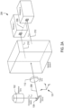
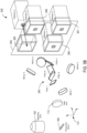
- FIG. 1 shows a schematic representation of an example microscopy instrument 100.
- the instrument 100 includes an objective lens 102, a polychroic mirror 104, an excitation filter 106, a light source 108, an emission filter 110, a tube lens 112, a splitting system 114, and a planar array of detectors 116.
- the light source 108 can be a laser that emits a high-intensity, substantially monochromatic beam of light 118.
- the excitation filter 106 and the polychroic mirror 104 transmit the beam of excitation light, which passes through the objective 102 and an aperture in a stage 120 to a specimen disposed on a microscope slide 122 that is supported by the stage 120.
- the excitation filter 106 prevents out-of-band wavelengths of light from entering the source 108.
- Components of the specimen are labeled with fluorescent probes. Each type of probe is designed to bind specifically to a particular component of the specimen, and each type of fluorophore is bound to a particular type of probe so that when the specimen is illuminated with the excitation light 118 the different fluorophores emit light with different wavelengths in the visible and near-visible portion of the electromagnetic spectrum. As a result, each component of the specimen is displayed with a different associated wavelength.
- the specimen components are labeled with N different types of fluorophores that each emits light of a different wavelength in the visible spectrum.
- Figure 1 includes a plot 124 of intensity versus a range of wavelengths in the visible spectrum. Each curve of the plot 124 represents an intensity distribution over a very narrow range of wavelengths centered about a particular wavelength. For example, curve 126 represents a narrow range of excitation wavelengths centered about a wavelength ⁇ ex 1 that produces an emission of light from a first type of fluorophore, and curve 128 represents a narrow range of emission wavelengths centered about a wavelength ⁇ em 1 emitted by the first fluorophore.
- the N excitation wavelengths denoted by ⁇ exi excite emission from the N different types of fluorophores.
- i is an integer index that ranges from 1 to N
- Each of the N different types of fluorophore emits a corresponding emission wavelength denoted by ⁇ emi .
- the N excitation wavelengths are called "excitation channels,” and the N wavelengths of light emitted from the N types of fluorophores are called “emission channels.”
- the N excitation channels ⁇ exi comprise the excitation light 118.
- a portion of the N emission channels is collected and collimated by the objective lens 102 into a single emission beam 130.
- the beam 130 is reflected from the polychroic mirror 104 to travel along a central optical emission axis that runs parallel to the z -axis of a Cartesian coordinate system 131 associated with the instrument 100.
- the beam 130 passes through the emission filter 110 which blocks stray excitation light.
- the tube lens 112 can represent a single lens or represent a number of lenses and other optical elements that focus the beam 130 onto an image plane at the detectors 116 before the beam 130 enters the splitting system 114.
- the splitting system 114 separates the emission channels of the beam 130 so that each channel follows one of N separate, substantially parallel paths through the emission filter(s) 110 to a detector in the planar array of detectors 116.
- directional arrows 132 and 134 represent substantially parallel output beams in which the output beam 132 is the emission channel ⁇ em 1 directed to the detector 136 and the output beam 134 is the emission channel ⁇ em 2 directed to the detector 138.
- Each detector in the array 116 can be a photodetector array, a CCD camera, or a CMOS camera. In an alternative embodiment, each beam can pass through a separate excitation filter.
- the splitting system 114 and the planar array of detectors 116 form a detection system of the instrument 100.
- the detectors in the array 116 can have any suitable arrangement but the detectors lie in approximately the same plane facing the splitting system 114.
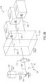
- Figures 2A-2D show four examples of detection systems that each represent a different planar arrangement of the detectors. Each figure includes the objective lens 102, the polychroic mirror 104, and the tube lens 112 described above.
- the detection system includes a splitting system 202 and an array of two detectors 204. The two detectors lie along a line 206 oriented parallel to the y -axis.
- the splitting system 202 receives an emission beam of light 208 composed of two emission channels ⁇ em 1 , and ⁇ em 2 and separates the two channels so that channel ⁇ em 1 is output in a beam 210 to the detector 1 and channel ⁇ em 2 is output in a beam 212 to the detector 2.
- the beams 210 and 212 lie in the yz -plane and are substantially parallel to one another.
- the detection system includes a splitting system 214 and an array of three detectors 216.
- the three detectors lie in the yz -plane.
- the splitting system 214 receives an emission beam of light 220 composed of three emission channels ⁇ em 1 , ⁇ em 2 and ⁇ em 3 and separates the channels so that channel ⁇ em 1 is output in a beam 222 to the detector 1, channel ⁇ em 2 is output in a beam 224 to the detector 2, and channel ⁇ em 3 is output in a beam 226 to the detector 3.
- the beams 222, 224, and 226 lie in the yz -plane and are substantially parallel to one another. Note that detector 2 is placed farther from the splitting system 214 than the detectors 1 and 3 in order for the optical path lengths traveled by the beams 222, 224, and 226 to be approximately the same. In other embodiments, the detectors can lie along a line oriented parallel to the xy-plane by including mirrors in the splitting system 214 that reflect the beam 224 internally in order to increase the optical path length of the beam 224 to approximately match the optical path length traveled by the beams 222 and 226.
- the detectors are not limited to being arranged along a line parallel to the y -direction, the linear arrays of detectors 204 and 216 can be arranged along any line that lies in the xy -plane.
- the output beams and the detectors can have a two-dimensional geometrical arrangement as represented in Figures 2C and 2D .
- the detection system includes a splitting system 228 and an array of three detectors 230. The three detectors are arranged so that each detector is located at a vertex of a triangle 232 oriented parallel to the xy-plane.
- the splitting system 228 receives the emission beam of light 220 and separates the channels so that channel ⁇ em 1 is output in a beam 234 to the detector 1, channel ⁇ em 2 is output in a beam 236 to the detector 2, and channel ⁇ em 3 is output in a beam 238 to the detector 3.
- the beams 234, 236, and 238 are substantially parallel to one another.
- the detection system includes a splitting system 240 and an array of four detectors 242 arranged so that each detector is located at a vertex of a rectangle 244 oriented parallel to the xy-plane.
- the splitting system 240 receives and separates an emission beam of light 246 composed of four channels so that channel ⁇ em 1 is output in a beam 248 to the detector 1, channel ⁇ em 2 is output in a beam 250 to the detector 2, channel ⁇ em 3 is output in a beam 252 to the detector 3, and channel ⁇ em 4 is output in a beam 254 to the detector 4.
- the beams 248, 250, 252, and 254 are substantially parallel to one another.
- Detection systems are not intended to be limited to planar arrays of up to four detectors.
- detection systems can have five or more detectors in a planar geometric arrangement.
- five detectors can be arranged so that the detectors are located at the vertices of a pentagon and six detectors can be arranged so that the detectors are located at the vertices of a hexagon.
- the detectors can have an irregular planar arrangement and are not intended to be limited to a planar, regular, two-dimensional geometrical arrangement.
- the planar arrangement of detectors on one side or to the back of a microscopy instrument as described above is compact, which minimizes the footprint of the instrument. With all of the detectors located on one side or to the back of the instrument, the instrument can be more rapidly and conveniently installed in a smaller area and all of the cables and coolant tubes used to operate the detectors protrude from one side of the instrument rather than the cables and coolant tubes protrude from a number of different sides of the instrument, which improves the aesthetics of the instrument.
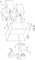
- Splitting systems can be implemented with a set of optical filters located along the emission axis of a microscopy instrument and a second set of mirrors positioned around the set of optical filters.
- Each filter is configured to reflect a particular channel to one of the mirrors while allowing transmission of other wavelengths.
- Each mirror is oriented to reflect one of the channels to a corresponding detector. The channels are reflected in substantially parallel output beams to the detectors as described above with reference to the examples shown in Figure 2 .
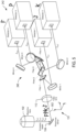
- Figure 3A shows an example implementation of the splitting system 240 of the detection system shown in Figure 2D .
- the splitting system 240 includes a set of four optical filters 1-4 arranged along an emission axis 302 that runs parallel to the z -axis and includes four mirrors 1-4 radially distributed around the set of filters.
- FIG. 3B shows an example of a schematic implementation of a back plate 304 with four detector mounts 306-309.
- the mounts have rectangular planar arrangement in the xy -plane.
- the four separate mounts also allow the position of each of the detectors to be adjusted in the xy -plane and in the z -direction, in order to correct for refraction due to the beams passing through the filters, chromatic aberrations and other sources of optical path length variation.
- the number of detectors of a microscopy system can be scaled up or down.
- a microscopy system that includes the detection system shown in Figure 3B can be scaled down from a four detector detection system 242 to a three, two or a single detector detection system by removing any one, two or three detectors and the corresponding filters.
- the detection system can be scaled up from a single, two or three detector detection system by placing detectors in the detector mounts and adding the corresponding filters to the splitting system.
- the corresponding filter 4 is added to the splitting system 240 and the detection system is scaled up from a three-detector system to a four-detector system.
- the corresponding filter 4 is removed from the splitting system 240 and the detection system is scaled down from a four-detector system to a three-detector system.
- the filters 1-4 can be dichroic mirrors or polychroic mirrors. Each filter reflects one of the channels to a corresponding mirror.
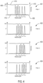
- Figure 4 shows example transmittance and reflectance plots 401-404 that represent the reflectance and transmittance properties associated with the filters 1-4, respectively.
- horizontal axes such as axis 406, represent wavelength
- vertical axes, such as axis 408, represent transmittance and reflectance as percentages
- vertical axes, such as axis 410 represent channel intensity
- dashed curves such as dashed curve 412, represent reflectance
- dotted curves such as dotted curve 414, represent transmittance.
- Each filter reflects one of the emission channels while transmitting other wavelengths.
- the example plots reveal that the filter 1 reflects the emission channel ⁇ em 1 , the filter 2 reflects the emission channel ⁇ em 2 , the filter 3 reflects the emission channel ⁇ em 3 , and the filter 4 reflects the emission channel ⁇ em 4 .
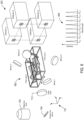
- Figure 5 shows the example splitting system 240 illustrated in Figure 3 in operation with the filters configured to reflect and transmit light as described with reference to Figure 4 .
- An emission beam 502 composed of the four channels ⁇ em 1 , ⁇ em 2 , ⁇ em 3 , and ⁇ em 4 is collected by the objective lens 102, reflected by the polychroic mirror 104 and collimated by the tube lens 112 before entering the splitting system 240.
- filter 1 reflects the channel ⁇ em 1 toward mirror 1 and transmits channels ⁇ em 2 , ⁇ em 3 , and ⁇ em 4 ;
- filter 2 reflects the channel ⁇ em 2 toward mirror 2 and transmits channels ⁇ em 3 , and ⁇ em 4 ;
- filter 3 reflects the channel ⁇ em 3 toward mirror 3 and transmits channel ⁇ em 4 ;
- filter 4 reflects the channel ⁇ em 4 toward mirror 4.
- the mirrors 104 are radially distributed around the set of filters 104 and are oriented so that each channel is reflected in an output beam that is substantially parallel to the output beams associated with the other channels.
- the mirrors 1-4 are oriented so that the respective channels ⁇ em 1 , ⁇ em 2 , ⁇ em 3 , and ⁇ em 4 are each reflected along separate, radially distributed, substantially parallel output beams to the detectors 1-4, respectively.
- the optical elements of the splitting systems are arranged to preserve the orientations of the images associated with the channels. For example, when a specimen is illuminated with excitation light and each type of fluorescently labeled component emits light in a different emission channel, each type of component has an associated image in a color that corresponds to the emission channel wavelength.
- the splitting system separates the different images according to the emission channel wavelengths and each image is captured by one of the detectors.
- the optical elements of the splitting system do not reorient the separate images of the components.
- Figure 5 also includes four letters "J,” “K,” “P,” and “F” that are used to represent the orientations of images of four different types of components of a specimen that are fluorescently labeled to emit light in the emission channels ⁇ em 1 , ⁇ em 2 , ⁇ em 3 , and ⁇ em 4 , respectively.
- the splitting system 240 separates the images according to the associated emission channel wavelengths, but the orientation of each image is preserved as the image is twice reflected and finally transmitted to a corresponding detector.
- the xy -plane orientations of the images associated with the letters “J,” “K,” “P,” and “F” just before entering the splitting system 240 are the same as the orientations of the letters “J,” “K,” “P,” and “F” in the xy-plane at the detectors 1-4. in other words, the images arrive at detectors 1-4 with the orientations of the images unchanged.
- a spitting system can have more than one set of filters.
- Each set of filters reflects a different set of emission channels.
- Figure 6 shows an example of a splitting system 602 with two sets of filters.
- each set of filters is mounted within a chassis that enables the sets to be switched by sliding the sets back and forth in the y -direction.
- Figure 6 includes an example plot 604 of two sets of emission channels associated with the filter sets 1 and 2.
- Filter set 1 is configured to reflect a first set of channels ⁇ em 1 , ⁇ em 2 , ⁇ em 3 , and ⁇ em 4 represented by solid-line peaks
- filter set 2 is configured to reflect a second set of channels ⁇ ' em 1 , , ⁇ ' em 2 , ⁇ ' em 3 . and ⁇ ' em 4 represented by dashed-line peaks.
- the filter set 1 When the filter set 1 is placed in the path of an emission beam composed of the two sets of channels, the set 1 separates the first set of channels ⁇ em 1 , ⁇ em 2 , ⁇ em 3 , and ⁇ em 4 in the manner described above with reference to Figure 5 .
- the filter set 2 When the filter set 2 is placed in the path of the emission beam, the set 2 separates the second set of channels ⁇ ' em 1 , ⁇ ' em 2 , ⁇ ' em 3 , and ⁇ ' em 4 in the manner described above.
- the locations of the excitation filter 106 and the light source 108 can be switched with the locations of the emission filter 110, tube lens 112, splitting system 114 and the planar array of detectors 116 and the polychroic mirror 104 can be replaced with a polychroic mirror that reflects the excitation beam 118 to the objective lens 102 and transmits the emission beam 130.
Description
- This disclosure claims the benefit of Provisional Application No.
61/511,093; filed July 24, 2011 - This disclosure relates to fluorescence microscopy and, in particular, to fluorescence microscopy instruments with camera systems.
- Multi-camera fluorescence microscopy provides a dedicated camera for each fluorescent emission channel allowing for improved speed and optical optimization. However, splitting the fluorescent emission channels into different optical paths and directing each emission channel to a separate camera often results in asymmetric and complicated optical systems. Consider for example a typical microscope with three cameras located on three different sides of the microscope. Light composed of three emission channels emitted from three different fluorescently labeled components of a specimen is collected by an objective lens. The light exits the objective lens and is split by the microscope optical system into three separate beams. Each beam is composed of light of one of the emission channels that travels along a separate optical path to one of the three cameras.
- However, because the cameras are located on different sides of the microscope, the camera cables and tubes used to transport coolant to the cameras project out of each side of the microscope that includes a camera. As a result, the footprint of the microscope can be large, which may be a problem when attempting to install the microscope in a limited lab space. In addition, the camera layout is asymmetric and irregular cabling and tube projections can substantially diminish the overall aesthetics of the microscope. For these reasons, engineers, scientists, and microscope manufacturers continue to seek microscopes with layouts that reduce the overall footprint of the microscope and are more aesthetically pleasing.
-
- Microscopy instruments with detectors located on one side of the instruments are disclosed. In one aspect, a microscopy instrument includes a splitting system and an array of detectors disposed on one side of the instrument. A beam composed of two or more separate emission channels travels along an emission path to the splitting system. The splitting system separates the emissions channels so that each emission channel travels along a separate path to one of the detectors in the array of detectors. The two or more paths travelled by the separate emission channels are substantially parallel so that each channel is received by a different detector in the array of detectors.
-
-
Figure 1 shows a schematic representation of an example microscopy instrument. -
Figures 2A-2D show four examples of detection systems associated with four microscopy instruments. -
Figure 3A shows an example implementation of a splitting system of the detection system shown inFigure 2D . -
Figure 3B shows an example of a schematic implementation of a back plate with four detector mounts. -
Figure 4 shows example transmittance and reflectance plots associated with optical filters of a splitting system. -
Figure 5 shows an example of a splitting system in operation. -
Figure 6 shows an example of a splitting system with two interchangeable sets of optical filters. -
Figure 1 shows a schematic representation of anexample microscopy instrument 100. Theinstrument 100 includes anobjective lens 102, apolychroic mirror 104, anexcitation filter 106, a light source 108, anemission filter 110, atube lens 112, asplitting system 114, and a planar array ofdetectors 116. The light source 108 can be a laser that emits a high-intensity, substantially monochromatic beam oflight 118. Theexcitation filter 106 and thepolychroic mirror 104 transmit the beam of excitation light, which passes through the objective 102 and an aperture in astage 120 to a specimen disposed on amicroscope slide 122 that is supported by thestage 120. Theexcitation filter 106 prevents out-of-band wavelengths of light from entering the source 108. Components of the specimen are labeled with fluorescent probes. Each type of probe is designed to bind specifically to a particular component of the specimen, and each type of fluorophore is bound to a particular type of probe so that when the specimen is illuminated with theexcitation light 118 the different fluorophores emit light with different wavelengths in the visible and near-visible portion of the electromagnetic spectrum. As a result, each component of the specimen is displayed with a different associated wavelength. In the example ofFigure 1 , the specimen components are labeled with N different types of fluorophores that each emits light of a different wavelength in the visible spectrum. The wavelengths are denoted by λi , where i is an integer index that ranges from 1 to N.Figure 1 includes aplot 124 of intensity versus a range of wavelengths in the visible spectrum. Each curve of theplot 124 represents an intensity distribution over a very narrow range of wavelengths centered about a particular wavelength. For example,curve 126 represents a narrow range of excitation wavelengths centered about a wavelength λ ex1 that produces an emission of light from a first type of fluorophore, andcurve 128 represents a narrow range of emission wavelengths centered about a wavelength λ em1 emitted by the first fluorophore. The N excitation wavelengths denoted by λexi , where i is an integer index that ranges from 1 to N, excite emission from the N different types of fluorophores. Each of the N different types of fluorophore emits a corresponding emission wavelength denoted by λemi . When the emission wavelengths are in the visible portion of the electromagnetic spectrum, the components appear in an image of the specimen with different colors. The N excitation wavelengths are called "excitation channels," and the N wavelengths of light emitted from the N types of fluorophores are called "emission channels." The N excitation channels λexi comprise theexcitation light 118. - A portion of the N emission channels is collected and collimated by the
objective lens 102 into asingle emission beam 130. Thebeam 130 is reflected from thepolychroic mirror 104 to travel along a central optical emission axis that runs parallel to the z-axis of a Cartesiancoordinate system 131 associated with theinstrument 100. Thebeam 130 passes through theemission filter 110 which blocks stray excitation light. Thetube lens 112 can represent a single lens or represent a number of lenses and other optical elements that focus thebeam 130 onto an image plane at thedetectors 116 before thebeam 130 enters thesplitting system 114. Thesplitting system 114 separates the emission channels of thebeam 130 so that each channel follows one of N separate, substantially parallel paths through the emission filter(s) 110 to a detector in the planar array ofdetectors 116. For example,directional arrows 132 and 134 represent substantially parallel output beams in which the output beam 132 is the emission channel λ em1 directed to thedetector 136 and theoutput beam 134 is the emission channel λ em2 directed to thedetector 138. Each detector in thearray 116 can be a photodetector array, a CCD camera, or a CMOS camera. In an alternative embodiment, each beam can pass through a separate excitation filter. Thesplitting system 114 and the planar array ofdetectors 116 form a detection system of theinstrument 100. The detectors in thearray 116 can have any suitable arrangement but the detectors lie in approximately the same plane facing thesplitting system 114. -
Figures 2A-2D show four examples of detection systems that each represent a different planar arrangement of the detectors. Each figure includes theobjective lens 102, thepolychroic mirror 104, and thetube lens 112 described above. In the example ofFigure 2A , the detection system includes a splitting system 202 and an array of twodetectors 204. The two detectors lie along aline 206 oriented parallel to the y-axis. The splitting system 202 receives an emission beam oflight 208 composed of two emission channels λ em1, and λ em2 and separates the two channels so that channel λ em1 is output in abeam 210 to thedetector 1 and channel λ em2 is output in abeam 212 to thedetector 2. Thebeams Figure 2B , the detection system includes asplitting system 214 and an array of threedetectors 216. The three detectors lie in the yz-plane. Thesplitting system 214 receives an emission beam oflight 220 composed of three emission channels λ em1, λ em2 and λ em3 and separates the channels so that channel λ em1 is output in abeam 222 to thedetector 1, channel λ em2 is output in abeam 224 to thedetector 2, and channel λ em3 is output in abeam 226 to thedetector 3. Thebeams detector 2 is placed farther from thesplitting system 214 than thedetectors beams splitting system 214 that reflect thebeam 224 internally in order to increase the optical path length of thebeam 224 to approximately match the optical path length traveled by thebeams detectors Figures 2C and2D . In the example ofFigure 2C , the detection system includes asplitting system 228 and an array of threedetectors 230. The three detectors are arranged so that each detector is located at a vertex of atriangle 232 oriented parallel to the xy-plane. In this example, thesplitting system 228 receives the emission beam oflight 220 and separates the channels so that channel λ em1 is output in abeam 234 to thedetector 1, channel λ em2 is output in abeam 236 to thedetector 2, and channel λ em3 is output in abeam 238 to thedetector 3. Thebeams Figure 2D , the detection system includes asplitting system 240 and an array of fourdetectors 242 arranged so that each detector is located at a vertex of a rectangle 244 oriented parallel to the xy-plane. In this example, thesplitting system 240 receives and separates an emission beam oflight 246 composed of four channels so that channel λ em1 is output in abeam 248 to thedetector 1, channel λ em2 is output in abeam 250 to thedetector 2, channel λ em3 is output in abeam 252 to thedetector 3, and channel λ em4 is output in abeam 254 to thedetector 4. Thebeams - Detection systems are not intended to be limited to planar arrays of up to four detectors. In other embodiments, detection systems can have five or more detectors in a planar geometric arrangement. For example, five detectors can be arranged so that the detectors are located at the vertices of a pentagon and six detectors can be arranged so that the detectors are located at the vertices of a hexagon. In other embodiments, the detectors can have an irregular planar arrangement and are not intended to be limited to a planar, regular, two-dimensional geometrical arrangement.
- The planar arrangement of detectors on one side or to the back of a microscopy instrument as described above is compact, which minimizes the footprint of the instrument. With all of the detectors located on one side or to the back of the instrument, the instrument can be more rapidly and conveniently installed in a smaller area and all of the cables and coolant tubes used to operate the detectors protrude from one side of the instrument rather than the cables and coolant tubes protrude from a number of different sides of the instrument, which improves the aesthetics of the instrument. Splitting systems can be implemented with a set of optical filters located along the emission axis of a microscopy instrument and a second set of mirrors positioned around the set of optical filters. Each filter is configured to reflect a particular channel to one of the mirrors while allowing transmission of other wavelengths. Each mirror is oriented to reflect one of the channels to a corresponding detector. The channels are reflected in substantially parallel output beams to the detectors as described above with reference to the examples shown in
Figure 2 .Figure 3A shows an example implementation of thesplitting system 240 of the detection system shown inFigure 2D . Thesplitting system 240 includes a set of four optical filters 1-4 arranged along anemission axis 302 that runs parallel to the z-axis and includes four mirrors 1-4 radially distributed around the set of filters. - In practice, the detectors of a detection system are attached to detector mounts in a back of a microscopy instrument and the detectors and the positions of the detectors can be varied slightly with respect to their distance from an ideal plane.
Figure 3B shows an example of a schematic implementation of aback plate 304 with four detector mounts 306-309. The mounts have rectangular planar arrangement in the xy-plane. As a result, when the detectors 1-4 are inserted into the corresponding mounts 306-309, the detectors 1-4 are substantially planar. The four separate mounts also allow the position of each of the detectors to be adjusted in the xy-plane and in the z-direction, in order to correct for refraction due to the beams passing through the filters, chromatic aberrations and other sources of optical path length variation. - The number of detectors of a microscopy system can be scaled up or down. In other words, a microscopy system that includes the detection system shown in
Figure 3B can be scaled down from a fourdetector detection system 242 to a three, two or a single detector detection system by removing any one, two or three detectors and the corresponding filters. Likewise, the detection system can be scaled up from a single, two or three detector detection system by placing detectors in the detector mounts and adding the corresponding filters to the splitting system. For example, inFigure 3B , when thedetector 4 is added to themount 309, thecorresponding filter 4 is added to thesplitting system 240 and the detection system is scaled up from a three-detector system to a four-detector system. Alternatively, when thedetector 4 is removed from themount 309, thecorresponding filter 4 is removed from thesplitting system 240 and the detection system is scaled down from a four-detector system to a three-detector system. - The filters 1-4 can be dichroic mirrors or polychroic mirrors. Each filter reflects one of the channels to a corresponding mirror.
Figure 4 shows example transmittance and reflectance plots 401-404 that represent the reflectance and transmittance properties associated with the filters 1-4, respectively. In each plot horizontal axes, such asaxis 406, represent wavelength; vertical axes, such asaxis 408, represent transmittance and reflectance as percentages; vertical axes, such asaxis 410, represent channel intensity; dashed curves, such as dashedcurve 412, represent reflectance; and dotted curves, such asdotted curve 414, represent transmittance. Each filter reflects one of the emission channels while transmitting other wavelengths. In particular, the example plots reveal that thefilter 1 reflects the emission channel λ em1, thefilter 2 reflects the emission channel λ em2, thefilter 3 reflects the emission channel λ em3, and thefilter 4 reflects the emission channel λ em4. -
Figure 5 shows theexample splitting system 240 illustrated inFigure 3 in operation with the filters configured to reflect and transmit light as described with reference toFigure 4 . Anemission beam 502 composed of the four channels λ em1, λ em2, λ em3, and λ em4 is collected by theobjective lens 102, reflected by thepolychroic mirror 104 and collimated by thetube lens 112 before entering thesplitting system 240. As theemission beam 502 passes through thesplitting system 240,filter 1 reflects the channel λ em1 towardmirror 1 and transmits channels λ em2, λ em3, and λ em4;filter 2 reflects the channel λ em2 towardmirror 2 and transmits channels λ em3, and λ em4;filter 3 reflects the channel λ em3 towardmirror 3 and transmits channel λ em4; andfilter 4 reflects the channel λ em4 towardmirror 4. As shown in the example ofFigure 5 , themirrors 104 are radially distributed around the set offilters 104 and are oriented so that each channel is reflected in an output beam that is substantially parallel to the output beams associated with the other channels. In particular, as shown inFigure 5 , the mirrors 1-4 are oriented so that the respective channels λ em1, λ em2, λ em3, and λ em4 are each reflected along separate, radially distributed, substantially parallel output beams to the detectors 1-4, respectively. - The optical elements of the splitting systems are arranged to preserve the orientations of the images associated with the channels. For example, when a specimen is illuminated with excitation light and each type of fluorescently labeled component emits light in a different emission channel, each type of component has an associated image in a color that corresponds to the emission channel wavelength. The splitting system separates the different images according to the emission channel wavelengths and each image is captured by one of the detectors. The optical elements of the splitting system do not reorient the separate images of the components.
Figure 5 also includes four letters "J," "K," "P," and "F" that are used to represent the orientations of images of four different types of components of a specimen that are fluorescently labeled to emit light in the emission channels λ em1, λ em2, λ em3, and λ em4, respectively. Thesplitting system 240 separates the images according to the associated emission channel wavelengths, but the orientation of each image is preserved as the image is twice reflected and finally transmitted to a corresponding detector. For example, the xy-plane orientations of the images associated with the letters "J," "K," "P," and "F" just before entering thesplitting system 240 are the same as the orientations of the letters "J," "K," "P," and "F" in the xy-plane at the detectors 1-4. in other words, the images arrive at detectors 1-4 with the orientations of the images unchanged. - In other embodiments, a spitting system can have more than one set of filters. Each set of filters reflects a different set of emission channels.
Figure 6 shows an example of asplitting system 602 with two sets of filters. In the example ofFigure 6 , each set of filters is mounted within a chassis that enables the sets to be switched by sliding the sets back and forth in the y-direction.Figure 6 includes anexample plot 604 of two sets of emission channels associated with the filter sets 1 and 2. Filter set 1 is configured to reflect a first set of channels λ em1, λ em2, λ em3, and λ em4 represented by solid-line peaks, and filter set 2 is configured to reflect a second set of channels λ' em1, , λ' em2, λ' em3. and λ' em4 represented by dashed-line peaks. When the filter set 1 is placed in the path of an emission beam composed of the two sets of channels, theset 1 separates the first set of channels λ em1, λ em2, λ em3, and λ em4 in the manner described above with reference toFigure 5 . When the filter set 2 is placed in the path of the emission beam, theset 2 separates the second set of channels λ' em1, λ' em2, λ' em3, and λ' em4 in the manner described above. - The foregoing description, for purposes of explanation, used specific nomenclature to provide a thorough understanding of the disclosure. However, it will be apparent to one skilled in the art that the specific details are not required in order to practice the systems and methods described herein. The foregoing descriptions of specific examples are presented for purposes of illustration and description. They are not intended to be exhaustive of or to limit this disclosure to the precise forms described. For example, with reference to
Figure 1 , the locations of theexcitation filter 106 and the light source 108 can be switched with the locations of theemission filter 110,tube lens 112,splitting system 114 and the planar array ofdetectors 116 and thepolychroic mirror 104 can be replaced with a polychroic mirror that reflects theexcitation beam 118 to theobjective lens 102 and transmits theemission beam 130. Obviously, many modifications and variations are possible in view of the above teachings. The examples are shown and described in order to best explain the principles of this disclosure and practical applications, to thereby enable others skilled in the art to best utilize this disclosure and various examples with various modifications as are suited to the particular use contemplated. It is intended that the scope of this disclosure be defined by the following claims and their equivalents:
Claims (7)
- A fluorescence microscopy instrument (100) for capturing separate images of components of a specimen, the instrument comprising:a light source (108) configured to illuminate the specimen (122) with an excitation beam (118) of light that excites fluorescently labeled components to emit light in a number of different wavelength emission channels (130), each emission channel associated with a particular component;an objective lens (102) configured to capture and direct the emission channels into an emission beam;a splitting system (114) configured to receive the emission beam, separate the beam into the emission channels, and direct the emission channels into separate, substantially parallel paths, wherein the splitting system includes: a set of mirrors; and one or more sets of optical filters, wherein each filter in each set is configured to reflect one of the emission channels toward one of the mirrors, and each mirror is positioned and oriented to reflect the emission channel into one of the separate, substantially parallel paths; the instrument further comprising:a planar array of detector mounts (306-309) disposed on one side of the instrument; anda plurality of detectors (116), wherein each detector is disposed within one of the detector mounts to receive one of the channels;the instrument being characterized in that the channels have equal optical path lengths,in that the instrument comprises a tube lens (112) being arranged before the splitting system (114) and focusing the emission beam (130) onto an image plane at the detectors (116),and in that the detector mounts (306-309) are configured to allow the positions of the detectors (116) to be varied with respect to their distance from an ideal plane.
- The instrument of claim 1 further comprising a polychroic mirror configured to reflect the emission channels to the splitting system.
- The instrument of any one of claims 1 or 2, wherein the mirrors of the splitting system are radially distributed around the set of optical filters.
- The instrument of any one of claims 2 or 3, wherein the optical filters are dichroic mirrors or polychroic mirrors.
- The instrument of any one of claims 2 or 3, wherein the separate, substantially parallel paths have a two-dimensional geometrical arrangement.
- The instrument of any one of claims 2 to 5, wherein each detector further comprises a photodetector array, a CCD camera, or a CMOS camera.
- The instrument of any one of claims 2 to 6, wherein the splitting system is configured to preserve the orientation of the images associated with the components.
Applications Claiming Priority (2)
| Application Number | Priority Date | Filing Date | Title |
|---|---|---|---|
| US201161511093P | 2011-07-24 | 2011-07-24 | |
| PCT/SE2012/050820 WO2013015733A1 (en) | 2011-07-24 | 2012-07-10 | Microscopy instruments with detector arrays and beam splitting system |
Publications (4)
| Publication Number | Publication Date |
|---|---|
| EP2742382A1 EP2742382A1 (en) | 2014-06-18 |
| EP2742382A4 EP2742382A4 (en) | 2015-03-11 |
| EP2742382B1 EP2742382B1 (en) | 2018-04-18 |
| EP2742382B2 true EP2742382B2 (en) | 2023-08-02 |
Family
ID=47601361
Family Applications (1)
| Application Number | Title | Priority Date | Filing Date |
|---|---|---|---|
| EP12817277.2A Active EP2742382B2 (en) | 2011-07-24 | 2012-07-10 | Microscopy instruments with detector arrays and beam splitting system |
Country Status (4)
| Country | Link |
|---|---|
| US (1) | US9709787B2 (en) |
| EP (1) | EP2742382B2 (en) |
| JP (1) | JP6018635B2 (en) |
| WO (1) | WO2013015733A1 (en) |
Families Citing this family (4)
| Publication number | Priority date | Publication date | Assignee | Title |
|---|---|---|---|---|
| CN104116497B (en) * | 2014-07-22 | 2016-10-05 | 中国科学院自动化研究所 | Spy optical molecular image-guidance system and multispectral imaging method |
| US10876970B2 (en) * | 2016-04-12 | 2020-12-29 | The Board Of Regents Of The University Of Texas System | Light-sheet microscope with parallelized 3D image acquisition |
| US10228283B2 (en) * | 2016-08-12 | 2019-03-12 | Spectral Insights Private Limited | Spectral imaging system |
| CN108181282B (en) * | 2018-01-03 | 2019-03-15 | 宁波纳美致生物科技有限公司 | A kind of triple channel fluorescence localization super-resolution biology microscope system and method |
Citations (2)
| Publication number | Priority date | Publication date | Assignee | Title |
|---|---|---|---|---|
| US5982497A (en) † | 1998-07-09 | 1999-11-09 | Optical Insights, Llc | Multi-spectral two-dimensional imaging spectrometer |
| WO2011072228A1 (en) † | 2009-12-11 | 2011-06-16 | Massachusetts Institute Of Technology | Spectral imaging of photoluminescent materials |
Family Cites Families (23)
| Publication number | Priority date | Publication date | Assignee | Title |
|---|---|---|---|---|
| SE455646B (en) * | 1984-10-22 | 1988-07-25 | Radians Innova Ab | FLUORESCENT DEVICE |
| JPS62238427A (en) | 1986-04-09 | 1987-10-19 | Sony Corp | Method for measuring chromaticity of fluorescent surface |
| JPH04104243A (en) | 1990-08-24 | 1992-04-06 | Hitachi Ltd | Spectral image device |
| US5742054A (en) * | 1995-09-01 | 1998-04-21 | Innovative Lasers Corporation | Ultra-sensitive detection of contaminants in corrosive gas via intracavity laser spectroscopy (ILS) |
| US5689334A (en) | 1995-09-01 | 1997-11-18 | Innovative Lasers Corporation | Intracavity laser spectroscope for high sensitivity detection of contaminants |
| EP1403675B1 (en) | 1997-04-09 | 2006-06-14 | 1192062 Alberta Limited | Colour translating UV microscope |
| JP3772016B2 (en) | 1998-03-26 | 2006-05-10 | 日本放送協会 | Wavelength selective camera device |
| US6441972B1 (en) | 2000-06-13 | 2002-08-27 | Jon R. Lesniak | Optical image separator |
| US7005645B2 (en) | 2001-11-30 | 2006-02-28 | Air Liquide America L.P. | Apparatus and methods for launching and receiving a broad wavelength range source |
| JP3686898B2 (en) | 2003-01-09 | 2005-08-24 | 独立行政法人理化学研究所 | Fluorescence energy transfer analyzer |
| US7697975B2 (en) | 2003-06-03 | 2010-04-13 | British Colombia Cancer Agency | Methods and apparatus for fluorescence imaging using multiple excitation-emission pairs and simultaneous multi-channel image detection |
| CA2554222A1 (en) | 2004-01-21 | 2005-12-22 | Optical Insights, Llc | Method and apparatus for multi-mode spectral imaging |
| WO2006017811A2 (en) * | 2004-08-06 | 2006-02-16 | Compucyte Corporation | Multiple-color monochromatic light absorption and quantification of light absorption in a stained sample |
| US7190514B2 (en) | 2004-08-12 | 2007-03-13 | Yokogawa Electric Corporation | Confocal scanning microscope |
| KR100647317B1 (en) | 2005-02-03 | 2006-11-23 | 삼성전자주식회사 | Optical system for multi-channel fluorescence measurement of microfluidic chip and multi-channel fluorescence sample analyzer |
| DE102006044214B4 (en) | 2006-09-15 | 2016-11-17 | Leica Microsystems Cms Gmbh | Microscope, in particular a polarization and / or a fluorescence microscope |
| US7888624B1 (en) | 2006-11-24 | 2011-02-15 | Solid State Scientific Corporation | Simultaneous spectral imaging system including commonly filtered optical paths defined by focusing elements exhibiting disparate f-numbers |
| JP5445135B2 (en) * | 2007-11-27 | 2014-03-19 | 株式会社ニコン | Fluorescence microscope |
| EP2146234A1 (en) | 2008-07-15 | 2010-01-20 | Femtonics Kft. | Laser scanning microscope |
| EP2389606B1 (en) * | 2009-01-24 | 2019-08-28 | Ecole Polytechnique Federale De Lausanne (EPFL) EPFL-TTO | High-resolution microscopy and photolithography devices using focusing micromirrors |
| JP5371694B2 (en) * | 2009-10-26 | 2013-12-18 | オリンパス株式会社 | Microscope connection unit and microscope system |
| DE102009060490A1 (en) | 2009-12-22 | 2011-06-30 | Carl Zeiss Microlmaging GmbH, 07745 | High-resolution microscope and image splitter arrangement |
| US9547178B2 (en) * | 2012-08-15 | 2017-01-17 | Semrock. Inc. | Dichroic image splitter |
-
2012
- 2012-07-10 EP EP12817277.2A patent/EP2742382B2/en active Active
- 2012-07-10 US US14/234,425 patent/US9709787B2/en active Active
- 2012-07-10 WO PCT/SE2012/050820 patent/WO2013015733A1/en active Application Filing
- 2012-07-10 JP JP2014522789A patent/JP6018635B2/en active Active
Patent Citations (2)
| Publication number | Priority date | Publication date | Assignee | Title |
|---|---|---|---|---|
| US5982497A (en) † | 1998-07-09 | 1999-11-09 | Optical Insights, Llc | Multi-spectral two-dimensional imaging spectrometer |
| WO2011072228A1 (en) † | 2009-12-11 | 2011-06-16 | Massachusetts Institute Of Technology | Spectral imaging of photoluminescent materials |
Also Published As
| Publication number | Publication date |
|---|---|
| US20140158865A1 (en) | 2014-06-12 |
| EP2742382A1 (en) | 2014-06-18 |
| US9709787B2 (en) | 2017-07-18 |
| JP6018635B2 (en) | 2016-11-02 |
| EP2742382B1 (en) | 2018-04-18 |
| JP2014521953A (en) | 2014-08-28 |
| EP2742382A4 (en) | 2015-03-11 |
| WO2013015733A1 (en) | 2013-01-31 |
Similar Documents
| Publication | Publication Date | Title |
|---|---|---|
| US7601938B2 (en) | Imaging system, methodology, and applications employing reciprocal space optical design | |
| US7385168B2 (en) | Imaging system, methodology, and applications employing reciprocal space optical design | |
| US8994807B2 (en) | Microscopy system and method for creating three dimensional images using probe molecules | |
| JP7045382B2 (en) | Optical groups for microscope detection light, methods for microscopy, and microscopy | |
| JP6596001B2 (en) | Multifocal multiphoton imaging system and method | |
| US20120287244A1 (en) | Non-coherent light microscopy | |
| JP2009517662A (en) | Confocal imaging method and apparatus | |
| CN107003505B (en) | Line scanning, sample scanning, multi-mode confocal microscope | |
| US8785885B1 (en) | Fluorescence imaging module | |
| CN110118758B (en) | Scattering fluorescence bimodal flow type imaging system | |
| EP2742382B2 (en) | Microscopy instruments with detector arrays and beam splitting system | |
| JP7350936B2 (en) | High-throughput hyperspectral imaging system | |
| JP2020536279A (en) | Slide inventory check and reinsert system | |
| RU2510959C2 (en) | Device for analysing luminescent biological microchips | |
| CN103852458A (en) | Microscopic method based on wide field stimulated emission difference and microscopic device based on wide field stimulated emission difference | |
| WO2021159285A1 (en) | Optical imaging system and biochemical substance detection system using same | |
| WO2013142272A1 (en) | Multi-color confocal microscope and imaging methods | |
| CN110823854A (en) | Fluorescence spectrum detection system of microorganism | |
| JP2009019961A (en) | Fluorescence detecting system | |
| CN115291377A (en) | Optical fiber confocal microscopic endoscopic imaging device and method | |
| JP2016224368A (en) | Imaging apparatus and imaging system |
Legal Events
| Date | Code | Title | Description |
|---|---|---|---|
| PUAI | Public reference made under article 153(3) epc to a published international application that has entered the european phase |
Free format text: ORIGINAL CODE: 0009012 |
|
| 17P | Request for examination filed |
Effective date: 20140124 |
|
| AK | Designated contracting states |
Kind code of ref document: A1 Designated state(s): AL AT BE BG CH CY CZ DE DK EE ES FI FR GB GR HR HU IE IS IT LI LT LU LV MC MK MT NL NO PL PT RO RS SE SI SK SM TR |
|
| DAX | Request for extension of the european patent (deleted) | ||
| A4 | Supplementary search report drawn up and despatched |
Effective date: 20150209 |
|
| RIC1 | Information provided on ipc code assigned before grant |
Ipc: G02B 27/14 20060101AFI20150203BHEP Ipc: G01N 21/64 20060101ALI20150203BHEP Ipc: G02B 21/18 20060101ALI20150203BHEP |
|
| 17Q | First examination report despatched |
Effective date: 20150421 |
|
| STAA | Information on the status of an ep patent application or granted ep patent |
Free format text: STATUS: EXAMINATION IS IN PROGRESS |
|
| REG | Reference to a national code |
Ref country code: DE Ref legal event code: R079 Ref document number: 602012045416 Country of ref document: DE Free format text: PREVIOUS MAIN CLASS: G02B0027140000 Ipc: G01N0021640000 |
|
| GRAP | Despatch of communication of intention to grant a patent |
Free format text: ORIGINAL CODE: EPIDOSNIGR1 |
|
| STAA | Information on the status of an ep patent application or granted ep patent |
Free format text: STATUS: GRANT OF PATENT IS INTENDED |
|
| RIC1 | Information provided on ipc code assigned before grant |
Ipc: G01N 21/64 20060101AFI20170915BHEP Ipc: G02B 21/16 20060101ALI20170915BHEP Ipc: G02B 21/18 20060101ALI20170915BHEP Ipc: G02B 27/14 20060101ALI20170915BHEP |
|
| INTG | Intention to grant announced |
Effective date: 20171017 |
|
| GRAS | Grant fee paid |
Free format text: ORIGINAL CODE: EPIDOSNIGR3 |
|
| GRAA | (expected) grant |
Free format text: ORIGINAL CODE: 0009210 |
|
| STAA | Information on the status of an ep patent application or granted ep patent |
Free format text: STATUS: THE PATENT HAS BEEN GRANTED |
|
| AK | Designated contracting states |
Kind code of ref document: B1 Designated state(s): AL AT BE BG CH CY CZ DE DK EE ES FI FR GB GR HR HU IE IS IT LI LT LU LV MC MK MT NL NO PL PT RO RS SE SI SK SM TR |
|
| REG | Reference to a national code |
Ref country code: GB Ref legal event code: FG4D |
|
| REG | Reference to a national code |
Ref country code: CH Ref legal event code: EP |
|
| REG | Reference to a national code |
Ref country code: AT Ref legal event code: REF Ref document number: 991016 Country of ref document: AT Kind code of ref document: T Effective date: 20180515 |
|
| REG | Reference to a national code |
Ref country code: IE Ref legal event code: FG4D |
|
| REG | Reference to a national code |
Ref country code: DE Ref legal event code: R096 Ref document number: 602012045416 Country of ref document: DE |
|
| REG | Reference to a national code |
Ref country code: FR Ref legal event code: PLFP Year of fee payment: 7 |
|
| REG | Reference to a national code |
Ref country code: NL Ref legal event code: FP |
|
| RAP2 | Party data changed (patent owner data changed or rights of a patent transferred) |
Owner name: GE HEALTHCARE BIO-SCIENCES CORP. |
|
| REG | Reference to a national code |
Ref country code: LT Ref legal event code: MG4D |
|
| REG | Reference to a national code |
Ref country code: DE Ref legal event code: R081 Ref document number: 602012045416 Country of ref document: DE Owner name: LEICA MICROSYSTEMS CMS GMBH, DE Free format text: FORMER OWNER: GE HEALTHCARE BIO-SCIENCES CORP., PISCATAWAY, N.J., US Ref country code: DE Ref legal event code: R081 Ref document number: 602012045416 Country of ref document: DE Owner name: GLOBAL LIFE SCIENCES SOLUTIONS USA LLC (N. D. , US Free format text: FORMER OWNER: GE HEALTHCARE BIO-SCIENCES CORP., PISCATAWAY, N.J., US Ref country code: DE Ref legal event code: R081 Ref document number: 602012045416 Country of ref document: DE Owner name: GE HEALTHCARE BIO-SCIENCES CORP., MARLBOROUGH, US Free format text: FORMER OWNER: GE HEALTHCARE BIO-SCIENCES CORP., PISCATAWAY, N.J., US |
|
| PG25 | Lapsed in a contracting state [announced via postgrant information from national office to epo] |
Ref country code: ES Free format text: LAPSE BECAUSE OF FAILURE TO SUBMIT A TRANSLATION OF THE DESCRIPTION OR TO PAY THE FEE WITHIN THE PRESCRIBED TIME-LIMIT Effective date: 20180418 Ref country code: AL Free format text: LAPSE BECAUSE OF FAILURE TO SUBMIT A TRANSLATION OF THE DESCRIPTION OR TO PAY THE FEE WITHIN THE PRESCRIBED TIME-LIMIT Effective date: 20180418 Ref country code: SE Free format text: LAPSE BECAUSE OF FAILURE TO SUBMIT A TRANSLATION OF THE DESCRIPTION OR TO PAY THE FEE WITHIN THE PRESCRIBED TIME-LIMIT Effective date: 20180418 Ref country code: BG Free format text: LAPSE BECAUSE OF FAILURE TO SUBMIT A TRANSLATION OF THE DESCRIPTION OR TO PAY THE FEE WITHIN THE PRESCRIBED TIME-LIMIT Effective date: 20180718 Ref country code: FI Free format text: LAPSE BECAUSE OF FAILURE TO SUBMIT A TRANSLATION OF THE DESCRIPTION OR TO PAY THE FEE WITHIN THE PRESCRIBED TIME-LIMIT Effective date: 20180418 Ref country code: NO Free format text: LAPSE BECAUSE OF FAILURE TO SUBMIT A TRANSLATION OF THE DESCRIPTION OR TO PAY THE FEE WITHIN THE PRESCRIBED TIME-LIMIT Effective date: 20180718 Ref country code: PL Free format text: LAPSE BECAUSE OF FAILURE TO SUBMIT A TRANSLATION OF THE DESCRIPTION OR TO PAY THE FEE WITHIN THE PRESCRIBED TIME-LIMIT Effective date: 20180418 Ref country code: LT Free format text: LAPSE BECAUSE OF FAILURE TO SUBMIT A TRANSLATION OF THE DESCRIPTION OR TO PAY THE FEE WITHIN THE PRESCRIBED TIME-LIMIT Effective date: 20180418 |
|
| PG25 | Lapsed in a contracting state [announced via postgrant information from national office to epo] |
Ref country code: GR Free format text: LAPSE BECAUSE OF FAILURE TO SUBMIT A TRANSLATION OF THE DESCRIPTION OR TO PAY THE FEE WITHIN THE PRESCRIBED TIME-LIMIT Effective date: 20180719 Ref country code: HR Free format text: LAPSE BECAUSE OF FAILURE TO SUBMIT A TRANSLATION OF THE DESCRIPTION OR TO PAY THE FEE WITHIN THE PRESCRIBED TIME-LIMIT Effective date: 20180418 Ref country code: LV Free format text: LAPSE BECAUSE OF FAILURE TO SUBMIT A TRANSLATION OF THE DESCRIPTION OR TO PAY THE FEE WITHIN THE PRESCRIBED TIME-LIMIT Effective date: 20180418 Ref country code: RS Free format text: LAPSE BECAUSE OF FAILURE TO SUBMIT A TRANSLATION OF THE DESCRIPTION OR TO PAY THE FEE WITHIN THE PRESCRIBED TIME-LIMIT Effective date: 20180418 |
|
| PG25 | Lapsed in a contracting state [announced via postgrant information from national office to epo] |
Ref country code: PT Free format text: LAPSE BECAUSE OF FAILURE TO SUBMIT A TRANSLATION OF THE DESCRIPTION OR TO PAY THE FEE WITHIN THE PRESCRIBED TIME-LIMIT Effective date: 20180820 |
|
| REG | Reference to a national code |
Ref country code: DE Ref legal event code: R026 Ref document number: 602012045416 Country of ref document: DE |
|
| PLBI | Opposition filed |
Free format text: ORIGINAL CODE: 0009260 |
|
| PG25 | Lapsed in a contracting state [announced via postgrant information from national office to epo] |
Ref country code: RO Free format text: LAPSE BECAUSE OF FAILURE TO SUBMIT A TRANSLATION OF THE DESCRIPTION OR TO PAY THE FEE WITHIN THE PRESCRIBED TIME-LIMIT Effective date: 20180418 Ref country code: CZ Free format text: LAPSE BECAUSE OF FAILURE TO SUBMIT A TRANSLATION OF THE DESCRIPTION OR TO PAY THE FEE WITHIN THE PRESCRIBED TIME-LIMIT Effective date: 20180418 Ref country code: EE Free format text: LAPSE BECAUSE OF FAILURE TO SUBMIT A TRANSLATION OF THE DESCRIPTION OR TO PAY THE FEE WITHIN THE PRESCRIBED TIME-LIMIT Effective date: 20180418 Ref country code: DK Free format text: LAPSE BECAUSE OF FAILURE TO SUBMIT A TRANSLATION OF THE DESCRIPTION OR TO PAY THE FEE WITHIN THE PRESCRIBED TIME-LIMIT Effective date: 20180418 Ref country code: SK Free format text: LAPSE BECAUSE OF FAILURE TO SUBMIT A TRANSLATION OF THE DESCRIPTION OR TO PAY THE FEE WITHIN THE PRESCRIBED TIME-LIMIT Effective date: 20180418 |
|
| 26 | Opposition filed |
Opponent name: CARL ZEISS MICROSCOPY GMBH Effective date: 20190117 |
|
| PG25 | Lapsed in a contracting state [announced via postgrant information from national office to epo] |
Ref country code: IT Free format text: LAPSE BECAUSE OF FAILURE TO SUBMIT A TRANSLATION OF THE DESCRIPTION OR TO PAY THE FEE WITHIN THE PRESCRIBED TIME-LIMIT Effective date: 20180418 Ref country code: SM Free format text: LAPSE BECAUSE OF FAILURE TO SUBMIT A TRANSLATION OF THE DESCRIPTION OR TO PAY THE FEE WITHIN THE PRESCRIBED TIME-LIMIT Effective date: 20180418 |
|
| PLAX | Notice of opposition and request to file observation + time limit sent |
Free format text: ORIGINAL CODE: EPIDOSNOBS2 |
|
| PG25 | Lapsed in a contracting state [announced via postgrant information from national office to epo] |
Ref country code: MC Free format text: LAPSE BECAUSE OF FAILURE TO SUBMIT A TRANSLATION OF THE DESCRIPTION OR TO PAY THE FEE WITHIN THE PRESCRIBED TIME-LIMIT Effective date: 20180418 Ref country code: LU Free format text: LAPSE BECAUSE OF NON-PAYMENT OF DUE FEES Effective date: 20180710 |
|
| REG | Reference to a national code |
Ref country code: BE Ref legal event code: MM Effective date: 20180731 |
|
| PG25 | Lapsed in a contracting state [announced via postgrant information from national office to epo] |
Ref country code: BE Free format text: LAPSE BECAUSE OF NON-PAYMENT OF DUE FEES Effective date: 20180731 Ref country code: SI Free format text: LAPSE BECAUSE OF FAILURE TO SUBMIT A TRANSLATION OF THE DESCRIPTION OR TO PAY THE FEE WITHIN THE PRESCRIBED TIME-LIMIT Effective date: 20180418 |
|
| PLBB | Reply of patent proprietor to notice(s) of opposition received |
Free format text: ORIGINAL CODE: EPIDOSNOBS3 |
|
| PG25 | Lapsed in a contracting state [announced via postgrant information from national office to epo] |
Ref country code: MT Free format text: LAPSE BECAUSE OF NON-PAYMENT OF DUE FEES Effective date: 20180710 |
|
| RAP2 | Party data changed (patent owner data changed or rights of a patent transferred) |
Owner name: GLOBAL LIFE SCIENCES SOLUTIONS USA LLC |
|
| PG25 | Lapsed in a contracting state [announced via postgrant information from national office to epo] |
Ref country code: TR Free format text: LAPSE BECAUSE OF FAILURE TO SUBMIT A TRANSLATION OF THE DESCRIPTION OR TO PAY THE FEE WITHIN THE PRESCRIBED TIME-LIMIT Effective date: 20180418 |
|
| PG25 | Lapsed in a contracting state [announced via postgrant information from national office to epo] |
Ref country code: HU Free format text: LAPSE BECAUSE OF FAILURE TO SUBMIT A TRANSLATION OF THE DESCRIPTION OR TO PAY THE FEE WITHIN THE PRESCRIBED TIME-LIMIT; INVALID AB INITIO Effective date: 20120710 |
|
| PG25 | Lapsed in a contracting state [announced via postgrant information from national office to epo] |
Ref country code: CY Free format text: LAPSE BECAUSE OF FAILURE TO SUBMIT A TRANSLATION OF THE DESCRIPTION OR TO PAY THE FEE WITHIN THE PRESCRIBED TIME-LIMIT Effective date: 20180418 Ref country code: MK Free format text: LAPSE BECAUSE OF NON-PAYMENT OF DUE FEES Effective date: 20180418 |
|
| PG25 | Lapsed in a contracting state [announced via postgrant information from national office to epo] |
Ref country code: IS Free format text: LAPSE BECAUSE OF FAILURE TO SUBMIT A TRANSLATION OF THE DESCRIPTION OR TO PAY THE FEE WITHIN THE PRESCRIBED TIME-LIMIT Effective date: 20180818 |
|
| PLAB | Opposition data, opponent's data or that of the opponent's representative modified |
Free format text: ORIGINAL CODE: 0009299OPPO |
|
| R26 | Opposition filed (corrected) |
Opponent name: CARL ZEISS MICROSCOPY GMBH Effective date: 20190117 |
|
| REG | Reference to a national code |
Ref country code: AT Ref legal event code: UEP Ref document number: 991016 Country of ref document: AT Kind code of ref document: T Effective date: 20180418 |
|
| REG | Reference to a national code |
Ref country code: CH Ref legal event code: NV Representative=s name: BOVARD SA NEUCHATEL CONSEILS EN PROPRIETE INTE, CH Ref country code: CH Ref legal event code: PFA Owner name: GLOBAL LIFE SCIENCES SOLUTIONS USA LLC, US Free format text: FORMER OWNER: GE HEALTHCARE BIO-SCIENCES CORP., US |
|
| REG | Reference to a national code |
Ref country code: DE Ref legal event code: R081 Ref document number: 602012045416 Country of ref document: DE Owner name: LEICA MICROSYSTEMS CMS GMBH, DE Free format text: FORMER OWNER: GE HEALTHCARE BIO-SCIENCES CORP., MARLBOROUGH, MASS., US Ref country code: DE Ref legal event code: R081 Ref document number: 602012045416 Country of ref document: DE Owner name: GLOBAL LIFE SCIENCES SOLUTIONS USA LLC (N. D. , US Free format text: FORMER OWNER: GE HEALTHCARE BIO-SCIENCES CORP., MARLBOROUGH, MASS., US |
|
| REG | Reference to a national code |
Ref country code: NL Ref legal event code: HC Owner name: GLOBAL LIFE SCIENCES SOLUTIONS USA LLC; US Free format text: DETAILS ASSIGNMENT: CHANGE OF OWNER(S), CHANGE OF OWNER(S) NAME; FORMER OWNER NAME: GE HEALTHCARE BIO-SCIENCES CORP. Effective date: 20201127 |
|
| RAP2 | Party data changed (patent owner data changed or rights of a patent transferred) |
Owner name: LEICA MICROSYSTEMS CMS GMBH |
|
| REG | Reference to a national code |
Ref country code: AT Ref legal event code: HC Ref document number: 991016 Country of ref document: AT Kind code of ref document: T Owner name: GLOBAL LIFE SCIENCES SOLUTIONS USA LLC, US Effective date: 20210728 |
|
| REG | Reference to a national code |
Ref country code: NL Ref legal event code: PD Owner name: LEICA MICROSYSTEMS CMS GMBH; DE Free format text: DETAILS ASSIGNMENT: CHANGE OF OWNER(S), ASSIGNMENT; FORMER OWNER NAME: GLOBAL LIFE SCIENCES SOLUTIONS USA LLC Effective date: 20220706 |
|
| REG | Reference to a national code |
Ref country code: GB Ref legal event code: 732E Free format text: REGISTERED BETWEEN 20220721 AND 20220727 |
|
| REG | Reference to a national code |
Ref country code: DE Ref legal event code: R081 Ref document number: 602012045416 Country of ref document: DE Owner name: LEICA MICROSYSTEMS CMS GMBH, DE Free format text: FORMER OWNER: GLOBAL LIFE SCIENCES SOLUTIONS USA LLC (N. D. GES. D. STAATES DELAWARE), MARLBOROUGH, MA, US |
|
| PGFP | Annual fee paid to national office [announced via postgrant information from national office to epo] |
Ref country code: NL Payment date: 20220726 Year of fee payment: 11 |
|
| PGFP | Annual fee paid to national office [announced via postgrant information from national office to epo] |
Ref country code: IE Payment date: 20220719 Year of fee payment: 11 Ref country code: AT Payment date: 20220719 Year of fee payment: 11 |
|
| PGFP | Annual fee paid to national office [announced via postgrant information from national office to epo] |
Ref country code: CH Payment date: 20220726 Year of fee payment: 11 |
|
| REG | Reference to a national code |
Ref country code: AT Ref legal event code: PC Ref document number: 991016 Country of ref document: AT Kind code of ref document: T Owner name: LEICA MICROSYSTEMS CMS GMBH, DE Effective date: 20230117 |
|
| P01 | Opt-out of the competence of the unified patent court (upc) registered |
Effective date: 20230414 |
|
| PUAH | Patent maintained in amended form |
Free format text: ORIGINAL CODE: 0009272 |
|
| STAA | Information on the status of an ep patent application or granted ep patent |
Free format text: STATUS: PATENT MAINTAINED AS AMENDED |
|
| 27A | Patent maintained in amended form |
Effective date: 20230802 |
|
| AK | Designated contracting states |
Kind code of ref document: B2 Designated state(s): AL AT BE BG CH CY CZ DE DK EE ES FI FR GB GR HR HU IE IS IT LI LT LU LV MC MK MT NL NO PL PT RO RS SE SI SK SM TR |
|
| REG | Reference to a national code |
Ref country code: DE Ref legal event code: R102 Ref document number: 602012045416 Country of ref document: DE |
|
| PGFP | Annual fee paid to national office [announced via postgrant information from national office to epo] |
Ref country code: GB Payment date: 20230725 Year of fee payment: 12 |
|
| PGFP | Annual fee paid to national office [announced via postgrant information from national office to epo] |
Ref country code: FR Payment date: 20230725 Year of fee payment: 12 Ref country code: DE Payment date: 20230726 Year of fee payment: 12 |
|
| PG25 | Lapsed in a contracting state [announced via postgrant information from national office to epo] |
Ref country code: NL Free format text: LAPSE BECAUSE OF FAILURE TO SUBMIT A TRANSLATION OF THE DESCRIPTION OR TO PAY THE FEE WITHIN THE PRESCRIBED TIME-LIMIT Effective date: 20180418 |
|
| REG | Reference to a national code |
Ref country code: AT Ref legal event code: MK05 Ref document number: 991016 Country of ref document: AT Kind code of ref document: T Effective date: 20180418 |
|
| PG25 | Lapsed in a contracting state [announced via postgrant information from national office to epo] |
Ref country code: AT Free format text: LAPSE BECAUSE OF FAILURE TO SUBMIT A TRANSLATION OF THE DESCRIPTION OR TO PAY THE FEE WITHIN THE PRESCRIBED TIME-LIMIT Effective date: 20180418 |
|
| REG | Reference to a national code |
Ref country code: CH Ref legal event code: PL |