US9547178B2 - Dichroic image splitter - Google Patents

Dichroic image splitter Download PDF

Info

Publication number
US9547178B2
US9547178B2 US13/585,886 US201213585886A US9547178B2 US 9547178 B2 US9547178 B2 US 9547178B2 US 201213585886 A US201213585886 A US 201213585886A US 9547178 B2 US9547178 B2 US 9547178B2
Authority
US
United States
Prior art keywords
image
light
nb2o5
sio2
coated
Prior art date
Legal status (The legal status is an assumption and is not a legal conclusion. Google has not performed a legal analysis and makes no representation as to the accuracy of the status listed.)
Active, expires
Application number
US13/585,886
Other versions
US20140049630A1 (en
Inventor
Turan Erdogan
Ligang Wang
Prashant Prabhat
Current Assignee (The listed assignees may be inaccurate. Google has not performed a legal analysis and makes no representation or warranty as to the accuracy of the list.)
Idex Health and Science LLC
Original Assignee
Semrock Inc
Priority date (The priority date is an assumption and is not a legal conclusion. Google has not performed a legal analysis and makes no representation as to the accuracy of the date listed.)
Filing date
Publication date
Application filed by Semrock Inc filed Critical Semrock Inc
Priority to US13/585,886 priority Critical patent/US9547178B2/en
Assigned to SEMROCK, INC. reassignment SEMROCK, INC. ASSIGNMENT OF ASSIGNORS INTEREST (SEE DOCUMENT FOR DETAILS). Assignors: ERDOGAN, TURAN, PRABHAT, PRASHANT, WANG, LIGANG
Publication of US20140049630A1 publication Critical patent/US20140049630A1/en
Application granted granted Critical
Publication of US9547178B2 publication Critical patent/US9547178B2/en
Assigned to IDEX HEALTH & SCIENCE LLC reassignment IDEX HEALTH & SCIENCE LLC MERGER (SEE DOCUMENT FOR DETAILS). Assignors: SEMROCK, INC.
Active legal-status Critical Current
Adjusted expiration legal-status Critical

Links

Images

Classifications

    • GPHYSICS
    • G02OPTICS
    • G02BOPTICAL ELEMENTS, SYSTEMS OR APPARATUS
    • G02B27/00Optical systems or apparatus not provided for by any of the groups G02B1/00 - G02B26/00, G02B30/00
    • G02B27/10Beam splitting or combining systems
    • G02B27/1006Beam splitting or combining systems for splitting or combining different wavelengths
    • G02B27/1013Beam splitting or combining systems for splitting or combining different wavelengths for colour or multispectral image sensors, e.g. splitting an image into monochromatic image components on respective sensors
    • GPHYSICS
    • G02OPTICS
    • G02BOPTICAL ELEMENTS, SYSTEMS OR APPARATUS
    • G02B27/00Optical systems or apparatus not provided for by any of the groups G02B1/00 - G02B26/00, G02B30/00
    • G02B27/10Beam splitting or combining systems
    • G02B27/14Beam splitting or combining systems operating by reflection only
    • G02B27/141Beam splitting or combining systems operating by reflection only using dichroic mirrors
    • GPHYSICS
    • G02OPTICS
    • G02BOPTICAL ELEMENTS, SYSTEMS OR APPARATUS
    • G02B5/00Optical elements other than lenses
    • G02B5/20Filters
    • G02B5/26Reflecting filters
    • GPHYSICS
    • G02OPTICS
    • G02BOPTICAL ELEMENTS, SYSTEMS OR APPARATUS
    • G02B5/00Optical elements other than lenses
    • G02B5/20Filters
    • G02B5/28Interference filters
    • G02B5/285Interference filters comprising deposited thin solid films

Definitions

  • This invention generally relates to apparatus and methods for distinguishing image content according to wavelength and more particularly to a dichroic image splitter for spectral separation of image-bearing light.
  • Thin film interference filters are widely used in systems for optical measurement and analysis, such as Raman spectroscopy and fluorescence imaging, for example.
  • Thin film interference filters including optical edge filters, notch filters, and laser line filters (LLFs) are advantageously used in such systems to transmit light having specific wavelength bands and to block unwanted light that could otherwise constitute or generate spurious optical signals and swamp the signals to be detected and analyzed.
  • Dichroic beam splitters utilize interference filter effects to reflect certain wavelengths or ranges of wavelengths and transmit other wavelengths or ranges of wavelengths. Failure or poor performance of such filters compromises the performance of systems in which they are used.
  • Conventional design approaches for optical instruments that utilize thin-film filters are often constrained by inherent characteristics of these filters and long-standing practices for how these filters are designed and used.
  • FIG. 1 shows one type of imaging apparatus that is used for analysis of spectral characteristics of a sample.
  • a fluorescence microscopy system 10 has a light source 12 with an illumination lens L 2 that directs a beam of excitation energy, within a specific wavelength range, toward a sample 20 for analysis.
  • Optical fluorescence occurs when absorption of light of the excitation wavelength(s) causes emission of light at one or more longer wavelengths.
  • a succession of filters 22 , 24 , and a beam splitter 26 are used to isolate the different wavelength bands of light from sample 20 through lens L 1 to their appropriate paths, through lens L 3 , so that the desired emitted signal content, which can be at orders of magnitude lower than the excitation energy, can be properly sensed at a detector 30 , such as a camera or charge-coupled device (CCD).
  • a detector 30 such as a camera or charge-coupled device (CCD).
  • FIG. 2A shows a fluorescence microscopy system 50 that uses a beam splitter 52 as an image splitter to provide an image of a first wavelength band to a first detector 60 and an image of a second wavelength band to a second detector 62 .
  • Beam splitter 52 is at a 45 degree angle with respect to the propagation direction of incident light. Additional filters 56 and 58 are used to help further isolate the image content according to wavelength.
  • Lenses L 1 and L 2 function as objective and illumination lenses, respectively.
  • Lenses L 5 and L 6 serve to direct the image-bearing light to detectors 60 and 62 .
  • FIG. 2B shows a fluorescence microscopy system 70 that obtains two images and provides them on a single detector 30 .
  • Image-bearing light is directed from a lens L 7 to a beam splitter 32 that transmits one wavelength band toward a mirror 34 and reflects the complementary wavelength band.
  • the transmitted wavelength band reflects from mirror 34 and is directed toward a movable mirror 36 , through emission filter 58 , and through a lens L 8 toward detector 30 , forming a first image.
  • Light of the complementary wavelength band that had been reflected from beam splitter 32 is redirected by movable mirror 36 through emission filter 56 . This light also goes through lens L 8 and forms a second image on detector 30 .
  • FIGS. 2A and 2B provide workable solutions for separating images of first and second wavelength bands, but have a number of shortcomings.
  • the requirement for two detectors 60 and 62 in the FIG. 2A embodiment adds cost and complexity, significantly increasing the size of the microscopy apparatus.
  • Detectors 60 and 62 are orthogonal to each other in conventional apparatus; the proper positioning of detectors 60 and 62 requires a relatively bulky mounting arrangement.
  • Both of the FIG. 2A and FIG. 2B embodiments add a significant number of components, increasing the cost and overall weight and bulk of the microscopy system.
  • Dichroic filters and, more broadly, thin-film interference filters in general are conventionally designed to provide desired behavior for light that is incident over a small range of angles, typically angles that are near normal incidence. With many thin-film designs, light behaves well at the design angle of incidence; but this behavior can degrade rapidly as the incident light varies further from the design angle of incidence.
  • Conventional thin-film filter designs often exhibit high sensitivity to angle of incidence (AOI) and cone half angle (CHA). For this reason, conventional design practice avoids directing incident light that is at high incident angles (relative to normal) onto dichroic and other types of thin-film surfaces. This practice sets a number of constraints on how components are arranged for separating image-bearing light according to its spectral characteristics, often making it difficult to package optical components for image splitting in a compact configuration.
  • the present invention provides apparatus and methods that enable spectral separation of image-bearing light using a single dichroic surface. Contrary to conventional teaching and practice in the optical arts, embodiments of the present invention obtain wavelength separation by disposing a dichroic surface at a grazing angle to incident light. This enables spectral separation at a favorable location in the optical path for a microscope or other instrument and allows image detectors to be adjacently disposed with respect to each other or, in some embodiments, allows a single image detector to be used for forming separate images from light over different wavelength bands.
  • the present invention provides an optical image splitter disposed in the path of image-bearing light along an optical axis, the image splitter comprising a coated dichroic surface disposed at an angle of 15 degrees or less relative to incident light along the optical axis, the coated dichroic surface having a plurality of layers of material, the plurality of layers including layers having a first refractive index, n L , and layers having a second refractive index, n H , greater than the first refractive index, wherein the coated surface transmits light of at least a first wavelength range to form a first image at an image plane and reflects light of a second wavelength range to form a second image at the image plane.
  • FIG. 1 is a simplified schematic diagram showing components of a conventional fluorescence microscope imaging system.
  • FIG. 2A is a simplified schematic diagram showing components of a conventional fluorescence microscope imaging system having two detectors.
  • FIG. 2B is a simplified schematic diagram showing a conventional fluorescence microscope imaging system that forms two images on a single detector.
  • FIG. 2C is a schematic diagram that shows how incidence at a grazing angle can be expressed for a surface in the path of incident light.
  • FIG. 3A is a schematic diagram showing a simplified optical path for a conventional fluorescence microscope.
  • FIG. 3B is a schematic diagram showing a simplified optical path for a fluorescence microscope, with a narrower beam width of the image-bearing light.
  • FIG. 4A is a schematic diagram showing a dichroic surface at grazing incidence to the path of image-bearing light.
  • FIG. 4B is a schematic diagram that shows the enlarged beam splitter of the FIG. 4A arrangement.
  • FIG. 5A is a schematic diagram showing an alternate embodiment with an embedded dichroic surface at grazing incidence to the path of image-bearing light.
  • FIG. 5B is a schematic diagram that shows the enlarged embedded beam splitter of the FIG. 5A arrangement.
  • FIG. 5C is a schematic diagram that shows surfaces and components of the image splitting element formed as a composite prism.
  • FIG. 6A is a schematic diagram showing an alternate embodiment of the present invention that uses two adjacent image detectors.
  • FIG. 6B is a schematic diagram showing an alternate embodiment of the present invention that uses two adjacent image detectors that are substantially in parallel.
  • FIG. 7 is a graph showing a dichroic filter characteristic at a grazing incidence angle according to an embodiment of the present invention.
  • oblique is used herein to refer to an angular relationship that is other than substantially orthogonal or parallel, that is, at least about 5 degrees from any integer multiple of 90 degrees.
  • grazing angle refers to an angle of incidence relative to a surface plane of not more than 30 degrees. Alternately stated, relative to a normal to the surface, a grazing angle is 60 degrees or more from normal.
  • substantially parallel image planes as used herein relates to image planes that are parallel to within no more than about +/ ⁇ 15 degrees.
  • prism or “prism element” is used herein as it is understood in optics, to refer to a transparent optical element that is generally in the form of an n-sided polyhedron with flat surfaces upon which light can be incident and that is formed from a transparent, material that refracts light that enters and exits the element.
  • the material that forms a prism or prism element is typically solid, but may alternately comprise a liquid. It is understood that, in terms of shape and surface outline, the optical understanding of what constitutes a prism is less restrictive than the formal geometric definition of a prism and encompasses that more formal definition.
  • the term “prism” is also used in reference to a “composite” element, formed from two or more monolithic “component” prism elements that are glued or otherwise coupled together, including composite elements whose components are mechanically coupled but have a thin gap at the interface between them filled with air or epoxy, for example.
  • the terms “configured”, “treated”, or “formed” are used equivalently with respect to the fabrication of thin film filters designed to provide a particular spectral characteristic.
  • a surface is considered to be transmissive to a particular wavelength if it transmits at least 75 percent of the light that is incident at that wavelength.
  • a surface is considered to reflect a given wavelength of incident light if it reflects at least 80 percent of the light that is incident at that wavelength.
  • Embodiments of the present invention take an alternate approach to conventional methods for image splitting to obtain two images that differ according to spectral content.
  • Embodiments of the present invention provide an optical apparatus in which either a single imaging detector can be used for obtaining both of the images or two imaging detectors, adjacent to each other and in substantially the same plane or in substantially parallel planes, rather than orthogonal to each other, can be used for this purpose.
  • interference filters are conventionally designed for light incident over a small range of angles, typically with the light propagation direction at near normal incidence. As incident light varies further from normal incidence, the performance of the filter with wavelength can change significantly. For example, even the 45 degree angle of incidence shown in the example of FIG. 2A is less than optimal for obtaining very high performance levels of dichroic wavelength response. Where the light is not reasonably well collimated, such as with light at larger cone angles, some amount of leakage of unwanted light can occur in either the path of reflected light or the path of transmitted light.
  • Dichroic surfaces are thus typically not used with light incident at angles less than about 30 degrees relative to the surface plane, such as light at grazing angles as defined previously; alternately stated, dichroic surfaces are typically not used with light at angles exceeding about 60 degrees relative to a normal to the surface.
  • FIG. 2C shows how incidence at a grazing angle can be expressed for a surface S in the path of incident light I.
  • Angle ⁇ 1 is the angle between incident light I in a propagation direction along an optical axis OA and surface S.
  • Angle ⁇ 2 is the angle between the incident light I and a normal N to surface S.
  • grazing incidence occurs when angle ⁇ 1 is less than 30 degrees, so that angle ⁇ 2 of the light with respect to normal N exceeds 60 degrees.
  • grazing incidence is provided wherein angle ⁇ 1 is less than 20 degrees, so that angle ⁇ 2 exceeds 70 degrees.
  • grazing incidence is provided wherein angle ⁇ 1 is near 10 degrees, so that angle ⁇ 2 is near 80 degrees.
  • Embodiments of the present invention can provide separation of image content according to wavelength bands with angles of grazing incidence ⁇ 1 as low as about 7 degrees.
  • FIG. 3A shows a simplified optical path for a conventional fluorescence microscope.
  • Objective lens L 1 directs image-bearing light to a tube lens L 12 for forming an image of the sample on detector 30 , typically a CCD (charge-coupled diode) or CMOS (complementary metal-oxide semiconductor) sensor array or other imaging device.
  • detector 30 typically a CCD (charge-coupled diode) or CMOS (complementary metal-oxide semiconductor) sensor array or other imaging device.
  • lenses L 1 and L 12 are designed to provide the image over the full sensing area of detector 30 .
  • FIG. 3B shows an alternate embodiment of the optical path for a fluorescence microscope, used when providing an image that is roughly half the size of detector 30 .
  • the beam width is reduced in size.
  • the smaller beam results from collection of light from a smaller area on the object.
  • FIG. 4A and enlarged partial view in enlarged area E of FIG. 4B show an embodiment of the present invention using a dichroic surface 40 in the path of the narrowed beam of image-bearing light from tube lens L 12 for separating spectral components of the image-bearing light beam.
  • Dichroic surface 40 is at a grazing angle of incidence ⁇ of not more than 30 degrees from the direction of light propagation along optical axis OA.
  • Dichroic surface 40 splits the image-bearing incident light according to wavelength ranges into a first image 64 a and a second image 64 b , both images formed at detector circuitry disposed along an image plane Q.
  • the angle of incidence of image-bearing light is 60 degrees or more.
  • the angle of dichroic surface 40 relative to image plane Q or image detector 30 shown as angle ⁇ in FIG. 4B , is orthogonal to within +/ ⁇ 15 degrees; according to alternate embodiments of the present invention, angle ⁇ is closer to 90 degrees, so that dichroic surface 40 is orthogonal to detector 30 to within +/ ⁇ 10 degrees or to within +/ ⁇ 5 degrees or less.
  • Image detector 30 is correspondingly oblique with respect to the optical axis OA.
  • a first image 64 a of at least a first wavelength range is formed on one portion of detector 30 ; a second image 64 b of a second wavelength range is formed on the adjacent portion of detector 30 .
  • Images 64 a and 64 b may be immediately adjacent on detector 30 or may be separated by one or more boundary rows of pixels.
  • Dichroic surface 40 can be designed to have any number of suitable wavelength pass characteristics, so that dichroic surface 40 acts as a long wavelength pass (LWP) filter, a short wavelength pass (SWP) filter, a band pass filter, or a multiple band pass filter.
  • Dichroic surface 40 is formed on a glass plate or other sheet surface in an embodiment of the present invention.
  • Optional filters 46 and 48 are provided for further isolation of the respective images in each wavelength range.
  • dichroic surface 40 is embedded within a glass substrate 42 or other transparent substrate 42 , forming an embedded image splitting element 44 .
  • Optional filters 46 , 48 can be coated onto or attached to surfaces of substrate 42 or may be separately disposed.
  • FIG. 5C shows surfaces and components of image splitting element 44 , formed as a composite prism.
  • Dichroic surface 40 is formed along the interface between two optical prisms 45 and 47 , such as on the surface of either prism.
  • the image-bearing light from tube lens L 12 is incident on a surface 72 that is substantially orthogonal to the optical axis OA. This light is then incident at a grazing angle on embedded dichroic surface 40 .
  • the light of each wavelength band is then directed to one of two output surfaces 74 and 76 .
  • filters 46 and 48 are optionally formed on output surfaces 74 and 76 .
  • embodiments of the present invention using embedded image splitting element 44 extend the back focal distance of tube lens L 12 by a short distance.
  • FIG. 6A is a schematic diagram showing an alternate embodiment of the present invention that uses two adjacent image detectors 30 a and 30 b instead of a single detector.
  • Image splitting element 44 transmits light of at least a first wavelength range to form a first image on first image detector 30 a and reflects light of a second wavelength range to form a second image on a second image detector 30 b .
  • Dichroic surface 40 lies in a plane P that is orthogonal to image plane Q and thus orthogonal to each image detector 30 a and 30 b , to within +/ ⁇ 10 degrees.
  • FIG. 6B is a schematic diagram showing an alternate embodiment of the present invention in which image detectors 30 a and 30 b are substantially in parallel, as described herein, but are slightly folded inward, along line of intersection K 1 , toward image splitting element 44 by a few degrees, disposed along substantially parallel image planes Q′ and Q 1 ′ in slightly modified form.
  • This arrangement positions image detectors 30 a and 30 b and corresponding filters 46 and 48 so that they are more nearly parallel to the output faces of image splitting element 44 .
  • This arrangement allows a measure of compensation for slight focus differences between the two images; however, this difference is negligible in some embodiments of the present invention.
  • FIG. 7 is a graph showing a dichroic filter characteristic 80 at a grazing incidence angle according to an embodiment of the present invention.
  • characteristic 80 has the behavior of a band pass filter.
  • dashed line curves 82 and 84 show the emission characteristics of first and second fluorophore materials.
  • Interference filters are treated or formed to be wavelength-selective as a result of the interference effects that take place between incident and reflected waves at boundaries between interleaved layers of materials having different refractive indices.
  • Interference filters conventionally include a dielectric stack composed of multiple alternating layers of two or more dielectric materials having different refractive indices.
  • each of the respective interleaved layers of the filter stack is very thin, e.g., having an optical thickness (physical thickness times the refractive index of the layer) on the order of a quarter wavelength of light.
  • These layers may be deposited on one or more substrates (e.g., a glass substrate) and may be interleaved in various configurations to provide one or more band-pass, or band-rejection filter characteristics.
  • a filter that substantially reflects at least one band of wavelengths and substantially transmits at least a second band of wavelengths immediately adjacent to the first band, such that the filter enables separation of the two bands of wavelengths by redirecting the reflected band is conventionally called a “dichroic beam splitter,” or simply a “dichroic” filter.
  • Optical filters formed or configured according to embodiments of the present invention generally employ the basic structure of a thin film interference filter.
  • a plurality of discrete layers of material are deposited onto a surface of a substrate in some alternating or otherwise interleaved pattern as a filter stack, wherein the optical index between individual layers in the filter stack changes abruptly, rather than continuously or gradually.
  • the plurality of layers include at least a plurality of first layers having a first refractive index, n L interleaved with a plurality of second layers having a second refractive index, n H , greater than the first refractive index.
  • One or more additional layers having refractive indices not equal to either n H or n L may also be in the filter stack.
  • the addition of a third material or other additional materials in the thin film stack helps to fine-tune filter response.
  • the numerical differences between the index of refraction in the high and low index of refraction materials affects the number of layers required for forming a filter with a particular transmittance characteristic. Generally, where there is a small difference between the indices of refraction for the high and low index materials, a higher number of alternating layers must be used to achieve a particular transmittance (or optical density). Where the difference between the indices of refraction in the high and low index materials is larger, fewer alternating layers are needed for achieving the same transmittance (density) values.
  • a wide variety of materials may be used to form the plurality of discrete material layers in the filter stack.
  • metals metallic and non-metallic oxides, transparent polymeric materials, and so-called “soft” coatings, such as sodium aluminum fluoride (Na 3 AlF 6 ) and zinc sulfide (ZnS).
  • metallic oxides chosen from silicon dioxide (SiO 2 ), tantalum pentoxide (Ta 2 O 5 ), niobium pentoxide (Nb 2 O 5 ), hafnium dioxide (HfO 2 ), titanium dioxide (TiO 2 ), and aluminum pentoxide (Al 2 O 5 ).
  • the plurality of interleaved material layers may include at least two distinct materials.
  • the filters according to the present disclosure may include a plurality of distinct alternating Nb 2 O 5 and SiO 2 layers which have indices of refraction of 2.3 and 1.5, respectively.
  • the filters in accordance with the present disclosure may use an interleaved pattern with at least three distinct materials, such as distinct Nb 2 O 5 , SiO 2 , and Ta 2 O 5 layers, each layer having a characteristic index of refraction.
  • more than three materials and other combinations of materials may also be used within the interleaved layer pattern.
  • the filters in accordance with the present disclosure can be manufactured using deposition methods and techniques that are known in the art.
  • these filters may be made with a computer controlled ion beam sputtering system, such as is described in commonly assigned U.S. Pat. No. 7,068,430, which is incorporated herein by reference.
  • a computer controlled ion beam sputtering system such as is described in commonly assigned U.S. Pat. No. 7,068,430, which is incorporated herein by reference.
  • such a system is capable of depositing a plurality of discrete alternating material layers, wherein the thickness of each layer may be precisely controlled.
  • Filter designs that specify the layer arrangement in accordance with the present disclosure may be produced by known thin-film filter design techniques.
  • these filter designs may be produced by optimizing the filter spectra and structure of an initial design, such as a traditional multicavity Fabry Perot narrow band pass interference filter, against a target spectrum using known optical optimization routines.
  • Non-limiting examples of such optimization routines include the variable-metric or simplex methods implemented in standard commercial thin-film design software packages, such as TFCalc by Software Spectra, Inc. of Portland, Oreg., and The Essential Macleod by Thin Film Center, Inc., of Arlington, Ariz.
  • a detailed description of filter design techniques that can be used to produce filter designs according to the present disclosure may be found in U.S. Pat. No. 7,068,430, as noted previously.
  • dichroic surface 40 can be an interference filter of any of a number of types, including SWP, LWP, band pass, or multiple band pass filter, for example.
  • dichroic surface 40 is designed as a band pass filter in an optical configuration in which light outside the pass band is discarded. Referring to FIG. 6A , for example, light of the desired pass band goes to detector 30 a ; detector 30 b is not used and is replaced by a beam dump.
  • Embodiments of the present invention are advantageous for applications such as fluorescence microscopy using multiple fluorophores, for example.
  • An advantage provided by the thin film interference filter design for light at grazing angle incidence relates to high rejection levels for light outside the intended transmission band or bands.
  • OD optical density
  • T log 10
  • Conventional dichroic beam splitter designs, as described in the background section typically provide rejection of no better than about OD 1.5. This is, in large part, due to differences in how light of different polarizations behaves at near 45 degree incidence.
  • embodiments of the present invention are capable of higher rejection levels, greater than OD 3 in some embodiments and even approaching or better than about OD 6 with light at grazing incidence.
  • High rejection levels reduce the demands on emission filters ( 46 and 48 in FIGS. 4B and 5B-6B ) and can even allow one or both of these filters to be optional.
  • well less than 10% of the light that transmits through the dichroic coated surface is light of the unwanted wavelength range(s) and less than 10% of the light that is reflected from the coated surface is light of the wavelength(s) intended for transmission.
  • rejection of OD 3 is provided, so that no more than 0.1% of the light that transmits through the dichroic coated surface is light of the unwanted wavelength range(s).
  • the dichroic surface is designed as a band pass filter. Out-of-band rejection levels approach or exceed OD 6. Thus, less than about 0.0001% of the light that transmits through the dichroic coated surface is light of the unwanted wavelength range(s).
  • the image splitter of embodiments of the present invention provides images having different spectral content with incident light at a grazing angle.
  • This arrangement allows a single image detector to obtain both images of different spectral content or, alternately, allows the use of two adjacent image detectors.

Abstract

An optical image splitter disposed in the path of image-bearing light along an optical axis has a coated dichroic surface disposed at an angle of 15 degrees or less relative to incident light along the optical axis. The coated dichroic surface has a number of layers of material, the of layers including layers having a first refractive index, nL, and layers having a second refractive index, nH, greater than the first refractive index. The coated surface transmits light of at least a first wavelength range to form a first image at an image plane and reflects light of a second wavelength range to form a second image at the image plane.

Description

FIELD OF THE INVENTION
This invention generally relates to apparatus and methods for distinguishing image content according to wavelength and more particularly to a dichroic image splitter for spectral separation of image-bearing light.
BACKGROUND OF THE INVENTION
Thin film interference filters are widely used in systems for optical measurement and analysis, such as Raman spectroscopy and fluorescence imaging, for example. Thin film interference filters, including optical edge filters, notch filters, and laser line filters (LLFs) are advantageously used in such systems to transmit light having specific wavelength bands and to block unwanted light that could otherwise constitute or generate spurious optical signals and swamp the signals to be detected and analyzed. Dichroic beam splitters utilize interference filter effects to reflect certain wavelengths or ranges of wavelengths and transmit other wavelengths or ranges of wavelengths. Failure or poor performance of such filters compromises the performance of systems in which they are used. Conventional design approaches for optical instruments that utilize thin-film filters are often constrained by inherent characteristics of these filters and long-standing practices for how these filters are designed and used.
As an example of one type of system that relies heavily on thin-film filters and benefits from high performance filter design, the simplified schematic diagram of FIG. 1 shows one type of imaging apparatus that is used for analysis of spectral characteristics of a sample. A fluorescence microscopy system 10 has a light source 12 with an illumination lens L2 that directs a beam of excitation energy, within a specific wavelength range, toward a sample 20 for analysis. Optical fluorescence occurs when absorption of light of the excitation wavelength(s) causes emission of light at one or more longer wavelengths. A succession of filters 22, 24, and a beam splitter 26 are used to isolate the different wavelength bands of light from sample 20 through lens L1 to their appropriate paths, through lens L3, so that the desired emitted signal content, which can be at orders of magnitude lower than the excitation energy, can be properly sensed at a detector 30, such as a camera or charge-coupled device (CCD).
The detection problem becomes more complex when there are multiple emission wavelengths, such as where multiple fluorophores are used within the sample or multiple lines are detected in Raman spectroscopy. The simplified schematic diagram of FIG. 2A shows a fluorescence microscopy system 50 that uses a beam splitter 52 as an image splitter to provide an image of a first wavelength band to a first detector 60 and an image of a second wavelength band to a second detector 62. Beam splitter 52 is at a 45 degree angle with respect to the propagation direction of incident light. Additional filters 56 and 58 are used to help further isolate the image content according to wavelength. Lenses L1 and L2 function as objective and illumination lenses, respectively. Lenses L5 and L6 serve to direct the image-bearing light to detectors 60 and 62.
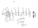
The simplified schematic diagram of FIG. 2B shows a fluorescence microscopy system 70 that obtains two images and provides them on a single detector 30. Image-bearing light is directed from a lens L7 to a beam splitter 32 that transmits one wavelength band toward a mirror 34 and reflects the complementary wavelength band. The transmitted wavelength band reflects from mirror 34 and is directed toward a movable mirror 36, through emission filter 58, and through a lens L8 toward detector 30, forming a first image. Light of the complementary wavelength band that had been reflected from beam splitter 32 is redirected by movable mirror 36 through emission filter 56. This light also goes through lens L8 and forms a second image on detector 30.
The arrangements of components shown in FIGS. 2A and 2B provide workable solutions for separating images of first and second wavelength bands, but have a number of shortcomings. The requirement for two detectors 60 and 62 in the FIG. 2A embodiment adds cost and complexity, significantly increasing the size of the microscopy apparatus. Detectors 60 and 62 are orthogonal to each other in conventional apparatus; the proper positioning of detectors 60 and 62 requires a relatively bulky mounting arrangement. Both of the FIG. 2A and FIG. 2B embodiments add a significant number of components, increasing the cost and overall weight and bulk of the microscopy system.
Dichroic filters and, more broadly, thin-film interference filters in general are conventionally designed to provide desired behavior for light that is incident over a small range of angles, typically angles that are near normal incidence. With many thin-film designs, light behaves well at the design angle of incidence; but this behavior can degrade rapidly as the incident light varies further from the design angle of incidence. Conventional thin-film filter designs often exhibit high sensitivity to angle of incidence (AOI) and cone half angle (CHA). For this reason, conventional design practice avoids directing incident light that is at high incident angles (relative to normal) onto dichroic and other types of thin-film surfaces. This practice sets a number of constraints on how components are arranged for separating image-bearing light according to its spectral characteristics, often making it difficult to package optical components for image splitting in a compact configuration.
Thus, it can be seen that there is a need for improved dichroic image splitter approaches for use in spectroscopy, fluorescence microscopy, and other applications.
SUMMARY OF THE INVENTION
It is an object of the present invention to advance the art of separating image content according to wavelength. With this object in mind, the present invention provides apparatus and methods that enable spectral separation of image-bearing light using a single dichroic surface. Contrary to conventional teaching and practice in the optical arts, embodiments of the present invention obtain wavelength separation by disposing a dichroic surface at a grazing angle to incident light. This enables spectral separation at a favorable location in the optical path for a microscope or other instrument and allows image detectors to be adjacently disposed with respect to each other or, in some embodiments, allows a single image detector to be used for forming separate images from light over different wavelength bands.
The present invention provides an optical image splitter disposed in the path of image-bearing light along an optical axis, the image splitter comprising a coated dichroic surface disposed at an angle of 15 degrees or less relative to incident light along the optical axis, the coated dichroic surface having a plurality of layers of material, the plurality of layers including layers having a first refractive index, nL, and layers having a second refractive index, nH, greater than the first refractive index, wherein the coated surface transmits light of at least a first wavelength range to form a first image at an image plane and reflects light of a second wavelength range to form a second image at the image plane.
Additional features and advantages will be set forth in part in the description which follows, being apparent from the description or learned by practice of the disclosed embodiments. The features and advantages will be realized and attained by means of the elements and combinations particularly pointed out in the appended claims.
It is to be understood that both the foregoing general description and the following detailed description are exemplary and explanatory only, and are not restrictive of the scope of the embodiments as claimed.
BRIEF DESCRIPTION OF THE DRAWINGS
While the specification concludes with claims particularly pointing out and distinctly claiming the subject matter of the present invention, it is believed that the invention will be better understood from the following description when taken in conjunction with the accompanying drawings.
FIG. 1 is a simplified schematic diagram showing components of a conventional fluorescence microscope imaging system.
FIG. 2A is a simplified schematic diagram showing components of a conventional fluorescence microscope imaging system having two detectors.
FIG. 2B is a simplified schematic diagram showing a conventional fluorescence microscope imaging system that forms two images on a single detector.
FIG. 2C is a schematic diagram that shows how incidence at a grazing angle can be expressed for a surface in the path of incident light.
FIG. 3A is a schematic diagram showing a simplified optical path for a conventional fluorescence microscope.
FIG. 3B is a schematic diagram showing a simplified optical path for a fluorescence microscope, with a narrower beam width of the image-bearing light.
FIG. 4A is a schematic diagram showing a dichroic surface at grazing incidence to the path of image-bearing light.
FIG. 4B is a schematic diagram that shows the enlarged beam splitter of the FIG. 4A arrangement.
FIG. 5A is a schematic diagram showing an alternate embodiment with an embedded dichroic surface at grazing incidence to the path of image-bearing light.
FIG. 5B is a schematic diagram that shows the enlarged embedded beam splitter of the FIG. 5A arrangement.
FIG. 5C is a schematic diagram that shows surfaces and components of the image splitting element formed as a composite prism.
FIG. 6A is a schematic diagram showing an alternate embodiment of the present invention that uses two adjacent image detectors.
FIG. 6B is a schematic diagram showing an alternate embodiment of the present invention that uses two adjacent image detectors that are substantially in parallel.
FIG. 7 is a graph showing a dichroic filter characteristic at a grazing incidence angle according to an embodiment of the present invention.
DETAILED DESCRIPTION OF THE INVENTION
It is to be understood that elements not specifically shown or described herein may take various forms well known to those skilled in the art. Figures shown and described herein are provided in order to illustrate key principles of operation and component relationships along their respective optical paths according to the present invention and are not drawn with intent to show actual size or scale. Some exaggeration may be necessary in order to more clearly emphasize basic structural relationships or principles of operation.
Where they are used, the terms “first”, “second”, “third”, and so on, do not necessarily denote any ordinal or priority relation, but are simply used to more clearly distinguish one element from another.
The term “oblique” is used herein to refer to an angular relationship that is other than substantially orthogonal or parallel, that is, at least about 5 degrees from any integer multiple of 90 degrees. The term “grazing angle” refers to an angle of incidence relative to a surface plane of not more than 30 degrees. Alternately stated, relative to a normal to the surface, a grazing angle is 60 degrees or more from normal.
The term “substantially parallel image planes” as used herein relates to image planes that are parallel to within no more than about +/−15 degrees.
The term “prism” or “prism element” is used herein as it is understood in optics, to refer to a transparent optical element that is generally in the form of an n-sided polyhedron with flat surfaces upon which light can be incident and that is formed from a transparent, material that refracts light that enters and exits the element. The material that forms a prism or prism element is typically solid, but may alternately comprise a liquid. It is understood that, in terms of shape and surface outline, the optical understanding of what constitutes a prism is less restrictive than the formal geometric definition of a prism and encompasses that more formal definition. In optics, for example, the term “prism” is also used in reference to a “composite” element, formed from two or more monolithic “component” prism elements that are glued or otherwise coupled together, including composite elements whose components are mechanically coupled but have a thin gap at the interface between them filled with air or epoxy, for example.
In the context of the present disclosure, the terms “configured”, “treated”, or “formed” are used equivalently with respect to the fabrication of thin film filters designed to provide a particular spectral characteristic. A surface is considered to be transmissive to a particular wavelength if it transmits at least 75 percent of the light that is incident at that wavelength. A surface is considered to reflect a given wavelength of incident light if it reflects at least 80 percent of the light that is incident at that wavelength.
The background section described some of the difficulties related to the design of a fluorescence or spectroscopic imaging apparatus that detects light emitted at multiple wavelengths. Embodiments of the present invention take an alternate approach to conventional methods for image splitting to obtain two images that differ according to spectral content. Embodiments of the present invention provide an optical apparatus in which either a single imaging detector can be used for obtaining both of the images or two imaging detectors, adjacent to each other and in substantially the same plane or in substantially parallel planes, rather than orthogonal to each other, can be used for this purpose.
As noted in the background section, interference filters are conventionally designed for light incident over a small range of angles, typically with the light propagation direction at near normal incidence. As incident light varies further from normal incidence, the performance of the filter with wavelength can change significantly. For example, even the 45 degree angle of incidence shown in the example of FIG. 2A is less than optimal for obtaining very high performance levels of dichroic wavelength response. Where the light is not reasonably well collimated, such as with light at larger cone angles, some amount of leakage of unwanted light can occur in either the path of reflected light or the path of transmitted light. Dichroic surfaces are thus typically not used with light incident at angles less than about 30 degrees relative to the surface plane, such as light at grazing angles as defined previously; alternately stated, dichroic surfaces are typically not used with light at angles exceeding about 60 degrees relative to a normal to the surface.
For clarification, the schematic diagram of FIG. 2C shows how incidence at a grazing angle can be expressed for a surface S in the path of incident light I. Angle θ1 is the angle between incident light I in a propagation direction along an optical axis OA and surface S. Angle θ2 is the angle between the incident light I and a normal N to surface S. For embodiments of the present invention, grazing incidence occurs when angle θ1 is less than 30 degrees, so that angle θ2 of the light with respect to normal N exceeds 60 degrees. According to an embodiment of the present invention, grazing incidence is provided wherein angle θ1 is less than 20 degrees, so that angle θ2 exceeds 70 degrees. According to another embodiment of the present invention, grazing incidence is provided wherein angle θ1 is near 10 degrees, so that angle θ2 is near 80 degrees. Embodiments of the present invention can provide separation of image content according to wavelength bands with angles of grazing incidence θ1 as low as about 7 degrees.
The schematic view of FIG. 3A shows a simplified optical path for a conventional fluorescence microscope. Objective lens L1 directs image-bearing light to a tube lens L12 for forming an image of the sample on detector 30, typically a CCD (charge-coupled diode) or CMOS (complementary metal-oxide semiconductor) sensor array or other imaging device. In conventional practice, as shown in FIG. 3A, lenses L1 and L12 are designed to provide the image over the full sensing area of detector 30.
FIG. 3B shows an alternate embodiment of the optical path for a fluorescence microscope, used when providing an image that is roughly half the size of detector 30. Here, the beam width is reduced in size. The smaller beam results from collection of light from a smaller area on the object.
The schematic diagram of FIG. 4A and enlarged partial view in enlarged area E of FIG. 4B show an embodiment of the present invention using a dichroic surface 40 in the path of the narrowed beam of image-bearing light from tube lens L12 for separating spectral components of the image-bearing light beam. Dichroic surface 40 is at a grazing angle of incidence α of not more than 30 degrees from the direction of light propagation along optical axis OA. Dichroic surface 40 splits the image-bearing incident light according to wavelength ranges into a first image 64 a and a second image 64 b, both images formed at detector circuitry disposed along an image plane Q. Relative to a normal to dichroic surface 40, the angle of incidence of image-bearing light is 60 degrees or more. The angle of dichroic surface 40 relative to image plane Q or image detector 30, shown as angle β in FIG. 4B, is orthogonal to within +/−15 degrees; according to alternate embodiments of the present invention, angle β is closer to 90 degrees, so that dichroic surface 40 is orthogonal to detector 30 to within +/−10 degrees or to within +/−5 degrees or less. Image detector 30 is correspondingly oblique with respect to the optical axis OA. A first image 64 a of at least a first wavelength range is formed on one portion of detector 30; a second image 64 b of a second wavelength range is formed on the adjacent portion of detector 30. Images 64 a and 64 b may be immediately adjacent on detector 30 or may be separated by one or more boundary rows of pixels. Dichroic surface 40 can be designed to have any number of suitable wavelength pass characteristics, so that dichroic surface 40 acts as a long wavelength pass (LWP) filter, a short wavelength pass (SWP) filter, a band pass filter, or a multiple band pass filter.
Dichroic surface 40 is formed on a glass plate or other sheet surface in an embodiment of the present invention. Optional filters 46 and 48 are provided for further isolation of the respective images in each wavelength range.
In an alternate embodiment of the present invention, as shown in the schematic diagrams of FIGS. 5A and 5B, dichroic surface 40 is embedded within a glass substrate 42 or other transparent substrate 42, forming an embedded image splitting element 44. Optional filters 46, 48 can be coated onto or attached to surfaces of substrate 42 or may be separately disposed.
The side view of FIG. 5C shows surfaces and components of image splitting element 44, formed as a composite prism. Dichroic surface 40 is formed along the interface between two optical prisms 45 and 47, such as on the surface of either prism. The image-bearing light from tube lens L12 is incident on a surface 72 that is substantially orthogonal to the optical axis OA. This light is then incident at a grazing angle on embedded dichroic surface 40. The light of each wavelength band is then directed to one of two output surfaces 74 and 76. In the embodiment shown in FIG. 5C, filters 46 and 48 are optionally formed on output surfaces 74 and 76.
It should be noted that embodiments of the present invention using embedded image splitting element 44 extend the back focal distance of tube lens L12 by a short distance.
FIG. 6A is a schematic diagram showing an alternate embodiment of the present invention that uses two adjacent image detectors 30 a and 30 b instead of a single detector. Image splitting element 44 transmits light of at least a first wavelength range to form a first image on first image detector 30 a and reflects light of a second wavelength range to form a second image on a second image detector 30 b. Dichroic surface 40 lies in a plane P that is orthogonal to image plane Q and thus orthogonal to each image detector 30 a and 30 b, to within +/−10 degrees. There is a line of intersection K1 defined by extending plane P into the image plane Q; this line of intersection K1 corresponds to a boundary between image content at image detectors 30 a and 30 b.
FIG. 6B is a schematic diagram showing an alternate embodiment of the present invention in which image detectors 30 a and 30 b are substantially in parallel, as described herein, but are slightly folded inward, along line of intersection K1, toward image splitting element 44 by a few degrees, disposed along substantially parallel image planes Q′ and Q1′ in slightly modified form. This arrangement positions image detectors 30 a and 30 b and corresponding filters 46 and 48 so that they are more nearly parallel to the output faces of image splitting element 44. This arrangement allows a measure of compensation for slight focus differences between the two images; however, this difference is negligible in some embodiments of the present invention.
FIG. 7 is a graph showing a dichroic filter characteristic 80 at a grazing incidence angle according to an embodiment of the present invention. Here, characteristic 80 has the behavior of a band pass filter. By way of reference, dashed line curves 82 and 84 show the emission characteristics of first and second fluorophore materials.
Fabrication
In general, thin-film interference filters are treated or formed to be wavelength-selective as a result of the interference effects that take place between incident and reflected waves at boundaries between interleaved layers of materials having different refractive indices. Interference filters conventionally include a dielectric stack composed of multiple alternating layers of two or more dielectric materials having different refractive indices. Moreover, in a conventional thin-film interference filter, each of the respective interleaved layers of the filter stack is very thin, e.g., having an optical thickness (physical thickness times the refractive index of the layer) on the order of a quarter wavelength of light. These layers may be deposited on one or more substrates (e.g., a glass substrate) and may be interleaved in various configurations to provide one or more band-pass, or band-rejection filter characteristics. A filter that substantially reflects at least one band of wavelengths and substantially transmits at least a second band of wavelengths immediately adjacent to the first band, such that the filter enables separation of the two bands of wavelengths by redirecting the reflected band, is conventionally called a “dichroic beam splitter,” or simply a “dichroic” filter.
Optical filters formed or configured according to embodiments of the present invention generally employ the basic structure of a thin film interference filter. In this basic structure, a plurality of discrete layers of material are deposited onto a surface of a substrate in some alternating or otherwise interleaved pattern as a filter stack, wherein the optical index between individual layers in the filter stack changes abruptly, rather than continuously or gradually. The plurality of layers include at least a plurality of first layers having a first refractive index, nL interleaved with a plurality of second layers having a second refractive index, nH, greater than the first refractive index. One or more additional layers having refractive indices not equal to either nH or nL may also be in the filter stack. In conventional thin film designs, two discrete layers are alternated, formed with thicknesses very near the quarter-wavelength thickness of some fundamental wavelength. In embodiments of the present invention, the addition of a third material or other additional materials in the thin film stack helps to fine-tune filter response. The numerical differences between the index of refraction in the high and low index of refraction materials affects the number of layers required for forming a filter with a particular transmittance characteristic. Generally, where there is a small difference between the indices of refraction for the high and low index materials, a higher number of alternating layers must be used to achieve a particular transmittance (or optical density). Where the difference between the indices of refraction in the high and low index materials is larger, fewer alternating layers are needed for achieving the same transmittance (density) values.
A wide variety of materials may be used to form the plurality of discrete material layers in the filter stack. Among such materials, non-limiting mention is made of metals, metallic and non-metallic oxides, transparent polymeric materials, and so-called “soft” coatings, such as sodium aluminum fluoride (Na3AlF6) and zinc sulfide (ZnS). Further non-limiting mention is made of metallic oxides chosen from silicon dioxide (SiO2), tantalum pentoxide (Ta2O5), niobium pentoxide (Nb2O5), hafnium dioxide (HfO2), titanium dioxide (TiO2), and aluminum pentoxide (Al2O5).
In some embodiments, the plurality of interleaved material layers may include at least two distinct materials. As a non-limiting example, the filters according to the present disclosure may include a plurality of distinct alternating Nb2O5 and SiO2 layers which have indices of refraction of 2.3 and 1.5, respectively. Alternatively, the filters in accordance with the present disclosure may use an interleaved pattern with at least three distinct materials, such as distinct Nb2O5, SiO2, and Ta2O5 layers, each layer having a characteristic index of refraction. Of course, more than three materials and other combinations of materials may also be used within the interleaved layer pattern.
Generally, the filters in accordance with the present disclosure can be manufactured using deposition methods and techniques that are known in the art. For example, these filters may be made with a computer controlled ion beam sputtering system, such as is described in commonly assigned U.S. Pat. No. 7,068,430, which is incorporated herein by reference. In general, such a system is capable of depositing a plurality of discrete alternating material layers, wherein the thickness of each layer may be precisely controlled.
Filter designs that specify the layer arrangement in accordance with the present disclosure may be produced by known thin-film filter design techniques. For example, these filter designs may be produced by optimizing the filter spectra and structure of an initial design, such as a traditional multicavity Fabry Perot narrow band pass interference filter, against a target spectrum using known optical optimization routines. Non-limiting examples of such optimization routines include the variable-metric or simplex methods implemented in standard commercial thin-film design software packages, such as TFCalc by Software Spectra, Inc. of Portland, Oreg., and The Essential Macleod by Thin Film Center, Inc., of Tucson, Ariz. A detailed description of filter design techniques that can be used to produce filter designs according to the present disclosure may be found in U.S. Pat. No. 7,068,430, as noted previously.
The layer structure for the dichroic image splitting surface with the spectral characteristic of FIG. 7 is provided subsequently in Table 1. As noted previously, dichroic surface 40 can be an interference filter of any of a number of types, including SWP, LWP, band pass, or multiple band pass filter, for example.
According to an alternate embodiment of the present invention, dichroic surface 40 is designed as a band pass filter in an optical configuration in which light outside the pass band is discarded. Referring to FIG. 6A, for example, light of the desired pass band goes to detector 30 a; detector 30 b is not used and is replaced by a beam dump.
Embodiments of the present invention are advantageous for applications such as fluorescence microscopy using multiple fluorophores, for example. An advantage provided by the thin film interference filter design for light at grazing angle incidence relates to high rejection levels for light outside the intended transmission band or bands. Rejection relates to the blocking ability of a filter and is expressed in optical density (OD), where, for transmission T, OD=−log10(T), so that −60 dB rejection is OD 6. Conventional dichroic beam splitter designs, as described in the background section, typically provide rejection of no better than about OD 1.5. This is, in large part, due to differences in how light of different polarizations behaves at near 45 degree incidence. By comparison, embodiments of the present invention are capable of higher rejection levels, greater than OD 3 in some embodiments and even approaching or better than about OD 6 with light at grazing incidence. High rejection levels reduce the demands on emission filters (46 and 48 in FIGS. 4B and 5B-6B) and can even allow one or both of these filters to be optional. According to an embodiment of the present invention, well less than 10% of the light that transmits through the dichroic coated surface is light of the unwanted wavelength range(s) and less than 10% of the light that is reflected from the coated surface is light of the wavelength(s) intended for transmission. According to another embodiment of the present invention, rejection of OD 3 is provided, so that no more than 0.1% of the light that transmits through the dichroic coated surface is light of the unwanted wavelength range(s). According to another embodiment of the present invention, the dichroic surface is designed as a band pass filter. Out-of-band rejection levels approach or exceed OD 6. Thus, less than about 0.0001% of the light that transmits through the dichroic coated surface is light of the unwanted wavelength range(s).
Unlike conventional beam splitters, the image splitter of embodiments of the present invention provides images having different spectral content with incident light at a grazing angle. This arrangement allows a single image detector to obtain both images of different spectral content or, alternately, allows the use of two adjacent image detectors. The invention has been described in detail with particular reference to certain preferred embodiments thereof, but it will be understood that variations and modifications can be effected within the scope of the invention as described above, and as noted in the appended claims, by a person of ordinary skill in the art without departing from the scope of the invention.
TABLES
TABLE 1
Dichroic Surface Layer Arrangement
Coating Thickness (μm): 16.349
NB2O5 (μm): 6.234
SIO2 (μm): 10.114
Number of Layers: 201
Thickness Accumulated
Layer Material (nm) (μm)
1 NB2O5 12.13300342 0.0121
2 SIO2 136.56480262 0.1487
3 NB2O5 105.19122086 0.2539
4 SIO2 109.93057811 0.3638
5 NB2O5 35.50481941 0.3993
6 SIO2 79.52943594 0.4789
7 NB2O5 103.46562405 0.5823
8 SIO2 119.43444818 0.7018
9 NB2O5 45.85088574 0.7476
10 SIO2 64.84444455 0.8124
11 NB2O5 81.12169754 0.8936
12 SIO2 127.23637213 1.0208
13 NB2O5 50.96814714 1.0718
14 SIO2 105.50438804 1.1773
15 NB2O5 49.89240806 1.2272
16 SIO2 116.97091408 1.3441
17 NB2O5 53.9223275 1.3981
18 SIO2 129.62526804 1.5277
19 NB2O5 53.42470785 1.5811
20 SIO2 114.02162743 1.6951
21 NB2O5 46.04365123 1.7412
22 SIO2 110.38818059 1.8516
23 NB2O5 62.15857358 1.9137
24 SIO2 136.97941752 2.0507
25 NB2O5 53.94463008 2.1047
26 SIO2 87.60207679 2.1923
27 NB2O5 51.54010068 2.2438
28 SIO2 128.88824105 2.3727
29 NB2O5 60.45663442 2.4331
30 SIO2 130.17660285 2.5633
31 NB2O5 48.18311945 2.6115
32 SIO2 99.46016927 2.711
33 NB2O5 51.26401495 2.7622
34 SIO2 137.45005855 2.8997
35 NB2O5 59.12107943 2.9588
36 SIO2 123.04736832 3.0818
37 NB2O5 47.0040482 3.1288
38 SIO2 101.76443361 3.2306
39 NB2O5 53.8276632 3.2844
40 SIO2 132.49526528 3.4169
41 NB2O5 61.93630516 3.4789
42 SIO2 107.13580575 3.586
43 NB2O5 49.68597111 3.6357
44 SIO2 99.60156678 3.7353
45 NB2O5 53.88844507 3.7892
46 SIO2 122.29512812 3.9115
47 NB2O5 81.87318843 3.9933
48 SIO2 80.15412173 4.0735
49 NB2O5 43.39439352 4.1169
50 SIO2 98.8597627 4.2158
51 NB2O5 98.38891915 4.3141
52 SIO2 82.80895411 4.397
53 NB2O5 44.89086912 4.4418
54 SIO2 114.0222875 4.5559
55 NB2O5 82.10374875 4.638
56 SIO2 84.18727763 4.7222
57 NB2O5 36.73860443 4.7589
58 SIO2 149.88160381 4.9088
59 NB2O5 92.17040016 5.0009
60 SIO2 107.01116971 5.108
61 NB2O5 34.13461534 5.1421
62 SIO2 110.25143593 5.2523
63 NB2O5 84.60827301 5.337
64 SIO2 120.35480417 5.4573
65 NB2O5 39.65801845 5.497
66 SIO2 95.53105952 5.5925
67 NB2O5 85.61458007 5.6781
68 SIO2 119.14616299 5.7973
69 NB2O5 32.02840156 5.8293
70 SIO2 121.63193964 5.9509
71 NB2O5 87.19274292 6.0381
72 SIO2 130.9356328 6.169
73 NB2O5 29.24988019 6.1983
74 SIO2 109.81458896 6.3081
75 NB2O5 94.38635433 6.4025
76 SIO2 113.87144232 6.5164
77 NB2O5 37.06350437 6.5534
78 SIO2 98.36608303 6.6518
79 NB2O5 80.17552826 6.732
80 SIO2 113.63428797 6.8456
81 NB2O5 40.49583036 6.8861
82 SIO2 79.43161201 6.9655
83 NB2O5 97.45028226 7.063
84 SIO2 118.01962154 7.181
85 NB2O5 40.60719438 7.2216
86 SIO2 87.65585544 7.3093
87 NB2O5 78.56449545 7.3878
88 SIO2 105.24813117 7.4931
89 NB2O5 44.6768247 7.5378
90 SIO2 95.21167323 7.633
91 NB2O5 68.08352353 7.7011
92 SIO2 96.91788288 7.798
93 NB2O5 50.72098285 7.8487
94 SIO2 91.70636041 7.9404
95 NB2O5 62.19064545 8.0026
96 SIO2 96.43924108 8.099
97 NB2O5 62.15666569 8.1612
98 SIO2 88.725655 8.2499
99 NB2O5 59.29509264 8.3092
100 SIO2 96.24074389 8.4054
101 NB2O5 60.4223968 8.4659
102 SIO2 87.77105283 8.5536
103 NB2O5 67.54728926 8.6212
104 SIO2 102.50046719 8.7237
105 NB2O5 59.11595012 8.7828
106 SIO2 81.65379492 8.8645
107 NB2O5 61.08184136 8.9255
108 SIO2 99.83699111 9.0254
109 NB2O5 71.06862545 9.0964
110 SIO2 88.97540985 9.1854
111 NB2O5 59.5568431 9.245
112 SIO2 89.40316338 9.3344
113 NB2O5 62.08644712 9.3965
114 SIO2 90.01841384 9.4865
115 NB2O5 67.99098177 9.5545
116 SIO2 91.94254761 9.6464
117 NB2O5 65.34547052 9.7118
118 SIO2 92.27398817 9.804
119 NB2O5 57.45666494 9.8615
120 SIO2 83.72282159 9.9452
121 NB2O5 70.50700486 10.0157
122 SIO2 104.40275996 10.1201
123 NB2O5 60.24252445 10.1804
124 SIO2 83.40146152 10.2638
125 NB2O5 66.62788869 10.3304
126 SIO2 97.04424739 10.4274
127 NB2O5 52.49034055 10.4799
128 SIO2 92.59636839 10.5725
129 NB2O5 84.74382459 10.6573
130 SIO2 96.00442336 10.7533
131 NB2O5 47.04394142 10.8003
132 SIO2 89.66166931 10.89
133 NB2O5 83.22186641 10.9732
134 SIO2 88.61094081 11.0618
135 NB2O5 45.67864564 11.1075
136 SIO2 99.55680689 11.2071
137 NB2O5 105.94516283 11.313
138 SIO2 91.70294582 11.4047
139 NB2O5 33.78792506 11.4385
140 SIO2 94.42802897 11.5329
141 NB2O5 114.14669337 11.6471
142 SIO2 110.21013622 11.7573
143 NB2O5 43.97282236 11.8012
144 SIO2 79.39078449 11.8806
145 NB2O5 77.78532895 11.9584
146 SIO2 90.83880903 12.0493
147 NB2O5 48.33969958 12.0976
148 SIO2 96.71109728 12.1943
149 NB2O5 81.71863281 12.276
150 SIO2 87.70536051 12.3637
151 NB2O5 46.06208991 12.4098
152 SIO2 92.25034084 12.5021
153 NB2O5 73.3294936 12.5754
154 SIO2 92.6305229 12.668
155 NB2O5 62.04287091 12.7301
156 SIO2 89.72715124 12.8198
157 NB2O5 54.70530059 12.8745
158 SIO2 88.17494698 12.9627
159 NB2O5 68.86582347 13.0315
160 SIO2 96.11054401 13.1276
161 NB2O5 65.10569428 13.1927
162 SIO2 89.61891435 13.2824
163 NB2O5 55.93281112 13.3383
164 SIO2 84.37723117 13.4227
165 NB2O5 67.58569409 13.4903
166 SIO2 100.11073416 13.5904
167 NB2O5 70.81052178 13.6612
168 SIO2 81.12046355 13.7423
169 NB2O5 52.74630117 13.795
170 SIO2 90.97647891 13.886
171 NB2O5 69.98953885 13.956
172 SIO2 90.14714225 14.0462
173 NB2O5 64.11095367 14.1103
174 SIO2 83.94143105 14.1942
175 NB2O5 53.09137398 14.2473
176 SIO2 92.01801387 14.3393
177 NB2O5 68.76541823 14.4081
178 SIO2 87.02863609 14.4951
179 NB2O5 63.61019637 14.5587
180 SIO2 93.0014373 14.6517
181 NB2O5 51.46678556 14.7032
182 SIO2 85.40577055 14.7886
183 NB2O5 81.11966268 14.8697
184 SIO2 103.04775869 14.9728
185 NB2O5 54.75608845 15.0275
186 SIO2 80.26881088 15.1078
187 NB2O5 68.15419148 15.1759
188 SIO2 95.36889911 15.2713
189 NB2O5 58.78582506 15.3301
190 SIO2 87.10092718 15.4172
191 NB2O5 79.18715941 15.4964
192 SIO2 97.75710711 15.5941
193 NB2O5 44.69236289 15.6388
194 SIO2 83.46653025 15.7223
195 NB2O5 91.7892229 15.8141
196 SIO2 127.12040273 15.9412
197 NB2O5 39.39829991 15.9806
198 SIO2 71.23438014 16.0518
199 NB2O5 92.18180183 16.144
200 SIO2 194.96613803 16.339
201 NB2O5 9.5322825 16.3485

Claims (19)

The invention claimed is:
1. A spectral splitting apparatus comprising:
an image plane that intersects an optical axis at an oblique angle; and
a coated dichroic surface that is orthogonal to the image plane to within +/−15 degrees, the coated dichroic surface having a plurality of layers of material, the plurality of layers including layers having a first refractive index, nL, and layers having a second refractive index, nH, greater than the first refractive index, wherein the coated dichroic surface intersects the optical axis at a grazing angle of 15 degrees or less relative to the optical axis, wherein the plurality of layers of material impart a spectral characteristic that, for an image-bearing light that is incident along the optical axis at the grazing angle, transmits light of at least a first wavelength range to form a first image at the image plane and reflects light outside the first wavelength range, to form a second image, spaced apart from the first image, at the same image plane.
2. The apparatus of claim 1 wherein the coated dichroic surface is encased within a transparent block.
3. The apparatus of claim 1 wherein the coated dichroic surface is orthogonal to the image plane to within +/−10 degrees.
4. The apparatus of claim 1 wherein there is a single image detector disposed at the image plane for detecting both first and second images.
5. The apparatus of claim 1 wherein there is a first image detector disposed at the image plane for detecting the first image and a second image detector disposed at the same image plane for detecting the second image.
6. The apparatus of claim 1 wherein less than 10% of the light that transmits through the dichroic coated surface is light of the second wavelength range.
7. The apparatus of claim 1 wherein less than 10% of the light that reflects from the dichroic coating is light of the first wavelength range.
8. The apparatus of claim 1 wherein less than 0.1% of the light that transmits through the dichroic coated surface is light of the second wavelength range.
9. The apparatus of claim 2 further comprising one or more output filters formed on one or more surfaces of the transparent block.
10. An optical image splitter having a coated dichroic surface disposed in the path of image-bearing light along an optical axis wherein the coated dichroic surface is configured to transmit light of at least a first wavelength range to form a first image at an intersection of the optical axis and an image plane that intersects the optical axis at an oblique angle and to reflect light of a second wavelength range,
wherein the coated dichroic surface is orthogonal to the image plane to within +/−10 degrees.
11. The optical image splitter of claim 10 wherein the first image is formed on a first image detector at the image plane and wherein the light of the second wavelength range forms a second image at a second image detector at the image plane.
12. The optical image splitter of claim 10 wherein the coated dichroic surface has a plurality of layers of material, the plurality of layers including layers having a first refractive index, nL, and layers having a second refractive index, nH, greater than the first refractive index.
13. The optical image splitter of claim 10 wherein the coated dichroic surface is encased within a transparent medium.
14. An imaging apparatus for viewing a sample, the apparatus comprising:
an optical system having an objective lens disposed to obtain light from the sample and a tube lens that directs image bearing light along an optical axis;
an optical image splitter disposed in the path of the image-bearing light along the optical axis and configured to transmit light of a first wavelength range to form a first image within a first image plane and to reflect light of a second wavelength range to form a second image within a second image plane,
wherein the first and second image planes are parallel to within +/−15 degrees, and
wherein the image splitter comprises a coated dichroic surface that is in a third plane that is orthogonal to each of the first and second image planes to within +/−10 degrees and wherein the third plane intersects the first and second image planes between the first and second images.
15. The apparatus of claim 14 wherein the image splitter is a composite prism element formed of first and second prisms with the coated dichroic surface formed along an interface of the first and second prisms.
16. The apparatus of claim 14 further comprising a single image detector that is disposed along both the first and second image planes.
17. The apparatus of claim 14 further comprising a first image detector that is disposed along the first image plane and a second image detector that is disposed along the second image plane.
18. The optical image splitter of claim 14 wherein less than 0.1% of the light that transmits through the dichroic coated surface is light of the second wavelength range.
19. An imaging apparatus comprising:
an optical system having an objective lens and a tube lens that define an optical axis;
an optical image splitter formed as a composite prism having:
a first prism element and a second prism element disposed to extend a back focal distance of the tube lens;
a dichroic surface formed along the interface between the first and second prism elements;
an incident surface substantially orthogonal to the optical axis;
first and second output surfaces that are both parallel to within +/−10 degrees of an output image plane Q,
and wherein the dichroic surface is at an angle β orthogonal to the output image plane Q to within +/−15 degrees and intersects the optical axis at an angle α of less than 30 degrees;
and
one or more image detectors disposed at the output image plane Q to obtain a first image formed by reflection of light from the optical system by the dichroic surface and a second image formed by transmission of light from the optical system by the dichroic surface.
US13/585,886 2012-08-15 2012-08-15 Dichroic image splitter Active 2034-08-24 US9547178B2 (en)

Priority Applications (1)

Application Number Priority Date Filing Date Title
US13/585,886 US9547178B2 (en) 2012-08-15 2012-08-15 Dichroic image splitter

Applications Claiming Priority (1)

Application Number Priority Date Filing Date Title
US13/585,886 US9547178B2 (en) 2012-08-15 2012-08-15 Dichroic image splitter

Publications (2)

Publication Number Publication Date
US20140049630A1 US20140049630A1 (en) 2014-02-20
US9547178B2 true US9547178B2 (en) 2017-01-17

Family

ID=50099788

Family Applications (1)

Application Number Title Priority Date Filing Date
US13/585,886 Active 2034-08-24 US9547178B2 (en) 2012-08-15 2012-08-15 Dichroic image splitter

Country Status (1)

Country Link
US (1) US9547178B2 (en)

Cited By (12)

* Cited by examiner, † Cited by third party
Publication number Priority date Publication date Assignee Title
US20140158865A1 (en) * 2011-07-24 2014-06-12 Ge Healthcare Bio-Sciences Corp. Microscopy instruments with detector arrays and beam splitting system
US20160291332A1 (en) * 2015-03-30 2016-10-06 Novadaq Technologies Inc. Multi-channel wide field imaging system and optical system for use therein
US10345237B1 (en) 2019-01-31 2019-07-09 Rarecyte, Inc. Spectral edge detection
US10656316B2 (en) 2015-08-31 2020-05-19 Novadaq Technologies ULC Polarization dependent filter, system using the same, and associated kits and methods
US10740884B2 (en) 2018-12-14 2020-08-11 Spectral Md, Inc. System and method for high precision multi-aperture spectral imaging
US10750992B2 (en) 2017-03-02 2020-08-25 Spectral Md, Inc. Machine learning systems and techniques for multispectral amputation site analysis
US10753875B1 (en) 2019-01-31 2020-08-25 Rarecyte, Inc. Spectral unmixing of spectroscopic emission images
US10783632B2 (en) 2018-12-14 2020-09-22 Spectral Md, Inc. Machine learning systems and method for assessment, healing prediction, and treatment of wounds
US10948638B2 (en) 2014-03-04 2021-03-16 Stryker European Operations Limited Spatial and spectral filtering apertures and optical imaging systems including the same
US11304604B2 (en) 2014-10-29 2022-04-19 Spectral Md, Inc. Reflective mode multi-spectral time-resolved optical imaging methods and apparatuses for tissue classification
US11631164B2 (en) 2018-12-14 2023-04-18 Spectral Md, Inc. System and method for high precision multi-aperture spectral imaging
US11948300B2 (en) 2018-12-14 2024-04-02 Spectral Md, Inc. Machine learning systems and methods for assessment, healing prediction, and treatment of wounds

Families Citing this family (1)

* Cited by examiner, † Cited by third party
Publication number Priority date Publication date Assignee Title
DE102016203749B4 (en) * 2016-03-08 2020-02-20 Carl Zeiss Smt Gmbh Optical system, especially for microscopy

Citations (19)

* Cited by examiner, † Cited by third party
Publication number Priority date Publication date Assignee Title
US1319292A (en) 1919-10-21 Light-dividing device
US2740317A (en) * 1951-08-13 1956-04-03 Technicolor Motion Picture Color selective optical interference coatings
US2945413A (en) * 1954-08-10 1960-07-19 Technicolor Corp Optical beam linking systems
US3905684A (en) 1972-09-19 1975-09-16 Rank Organisation Ltd Optical beam splitting system
US4268119A (en) 1979-01-22 1981-05-19 Bell & Howell Company Color-separating optical system
US4889426A (en) * 1987-10-22 1989-12-26 Carl-Zeiss-Stiftung Microscope photometer tube
US4933751A (en) 1987-09-09 1990-06-12 Victor Company Of Japan, Ltd. Tri-color separating optical system
US5926283A (en) 1997-07-12 1999-07-20 Optical Insights, Llc Multi-spectral two dimensional imaging spectrometer
US5982497A (en) 1998-07-09 1999-11-09 Optical Insights, Llc Multi-spectral two-dimensional imaging spectrometer
US6441972B1 (en) 2000-06-13 2002-08-27 Jon R. Lesniak Optical image separator
US20070132955A1 (en) 2003-03-14 2007-06-14 Victor Company Of Japan, Limited Image displaying apparatus and color separating-combining optical system
US20080055716A1 (en) * 2006-09-01 2008-03-06 Turan Erdogan Low cost filter for fluorescence systems
US20090244717A1 (en) 2008-03-28 2009-10-01 Contrast Optical Design & Engineering, Inc. Whole beam image splitting system
US7612822B2 (en) 2003-11-11 2009-11-03 Olympus Corporation Multispectral image capturing apparatus
US20100007852A1 (en) * 2008-07-11 2010-01-14 Bietry Joseph R Laser illuminated micro-mirror projector
US7649626B2 (en) 2002-04-18 2010-01-19 Qinetiq Limited Imaging spectrometer
US8081311B2 (en) 2005-11-04 2011-12-20 General Hospital Corporation System for multispectral imaging
US20120050877A1 (en) * 2010-08-24 2012-03-01 Fujifilm Corporation Color separating optical system
US20130208146A1 (en) * 2012-02-15 2013-08-15 Fluxdata, Inc. Method and apparatus for separate spectral imaging and sensing

Patent Citations (20)

* Cited by examiner, † Cited by third party
Publication number Priority date Publication date Assignee Title
US1319292A (en) 1919-10-21 Light-dividing device
US2740317A (en) * 1951-08-13 1956-04-03 Technicolor Motion Picture Color selective optical interference coatings
US2945413A (en) * 1954-08-10 1960-07-19 Technicolor Corp Optical beam linking systems
US3905684A (en) 1972-09-19 1975-09-16 Rank Organisation Ltd Optical beam splitting system
US4268119A (en) 1979-01-22 1981-05-19 Bell & Howell Company Color-separating optical system
US4933751A (en) 1987-09-09 1990-06-12 Victor Company Of Japan, Ltd. Tri-color separating optical system
US4889426A (en) * 1987-10-22 1989-12-26 Carl-Zeiss-Stiftung Microscope photometer tube
US5926283A (en) 1997-07-12 1999-07-20 Optical Insights, Llc Multi-spectral two dimensional imaging spectrometer
US5982497A (en) 1998-07-09 1999-11-09 Optical Insights, Llc Multi-spectral two-dimensional imaging spectrometer
US6441972B1 (en) 2000-06-13 2002-08-27 Jon R. Lesniak Optical image separator
US7649626B2 (en) 2002-04-18 2010-01-19 Qinetiq Limited Imaging spectrometer
US20070132955A1 (en) 2003-03-14 2007-06-14 Victor Company Of Japan, Limited Image displaying apparatus and color separating-combining optical system
US7612822B2 (en) 2003-11-11 2009-11-03 Olympus Corporation Multispectral image capturing apparatus
US7868936B2 (en) 2003-11-11 2011-01-11 Olympus Corporation Multispectral image capturing apparatus
US8081311B2 (en) 2005-11-04 2011-12-20 General Hospital Corporation System for multispectral imaging
US20080055716A1 (en) * 2006-09-01 2008-03-06 Turan Erdogan Low cost filter for fluorescence systems
US20090244717A1 (en) 2008-03-28 2009-10-01 Contrast Optical Design & Engineering, Inc. Whole beam image splitting system
US20100007852A1 (en) * 2008-07-11 2010-01-14 Bietry Joseph R Laser illuminated micro-mirror projector
US20120050877A1 (en) * 2010-08-24 2012-03-01 Fujifilm Corporation Color separating optical system
US20130208146A1 (en) * 2012-02-15 2013-08-15 Fluxdata, Inc. Method and apparatus for separate spectral imaging and sensing

Cited By (17)

* Cited by examiner, † Cited by third party
Publication number Priority date Publication date Assignee Title
US9709787B2 (en) * 2011-07-24 2017-07-18 Ge Healthcare Bio-Sciences Corp. Microscopy instruments with beam splitting system including optical filters and mirrors
US20140158865A1 (en) * 2011-07-24 2014-06-12 Ge Healthcare Bio-Sciences Corp. Microscopy instruments with detector arrays and beam splitting system
US10948638B2 (en) 2014-03-04 2021-03-16 Stryker European Operations Limited Spatial and spectral filtering apertures and optical imaging systems including the same
US11304604B2 (en) 2014-10-29 2022-04-19 Spectral Md, Inc. Reflective mode multi-spectral time-resolved optical imaging methods and apparatuses for tissue classification
US20160291332A1 (en) * 2015-03-30 2016-10-06 Novadaq Technologies Inc. Multi-channel wide field imaging system and optical system for use therein
US9989773B2 (en) * 2015-03-30 2018-06-05 Novadaq Technologies, Inc. Multi-channel wide field imaging system and optical system for use therein
US10656316B2 (en) 2015-08-31 2020-05-19 Novadaq Technologies ULC Polarization dependent filter, system using the same, and associated kits and methods
US11337643B2 (en) 2017-03-02 2022-05-24 Spectral Md, Inc. Machine learning systems and techniques for multispectral amputation site analysis
US10750992B2 (en) 2017-03-02 2020-08-25 Spectral Md, Inc. Machine learning systems and techniques for multispectral amputation site analysis
US10740884B2 (en) 2018-12-14 2020-08-11 Spectral Md, Inc. System and method for high precision multi-aperture spectral imaging
US10783632B2 (en) 2018-12-14 2020-09-22 Spectral Md, Inc. Machine learning systems and method for assessment, healing prediction, and treatment of wounds
US11182888B2 (en) 2018-12-14 2021-11-23 Spectral Md, Inc. System and method for high precision multi-aperture spectral imaging
US11948300B2 (en) 2018-12-14 2024-04-02 Spectral Md, Inc. Machine learning systems and methods for assessment, healing prediction, and treatment of wounds
US11631164B2 (en) 2018-12-14 2023-04-18 Spectral Md, Inc. System and method for high precision multi-aperture spectral imaging
US11599998B2 (en) 2018-12-14 2023-03-07 Spectral Md, Inc. Machine learning systems and methods for assessment, healing prediction, and treatment of wounds
US10345237B1 (en) 2019-01-31 2019-07-09 Rarecyte, Inc. Spectral edge detection
US10753875B1 (en) 2019-01-31 2020-08-25 Rarecyte, Inc. Spectral unmixing of spectroscopic emission images

Also Published As

Publication number Publication date
US20140049630A1 (en) 2014-02-20

Similar Documents

Publication Publication Date Title
US9547178B2 (en) Dichroic image splitter
TWI770168B (en) Induced transmission filter
US7773302B2 (en) Low cost filter for fluorescence systems
US9857511B2 (en) Interference filter for non-zero angle of incidence spectroscopy
JP6033898B2 (en) Tunable thin film filter
JP6932656B2 (en) Polarizing filter
US9423622B2 (en) Glass block dichroic beamsplitters
US7411679B2 (en) Optical filter and fluorescence spectroscopy system incorporating the same
WO2011158635A1 (en) Infrared blocking filter
CA2540376A1 (en) Partitioned-cavity tunable fabry-perot filter
CN105372801B (en) A kind of solar blind UV camera lens and system
US20180321463A1 (en) Mount for flat optical surface
US7298550B2 (en) Dichroic mirror, fluorescence filter set, and fluoroscopy apparatus
US9434145B2 (en) Dichroic filter conformed to optical surface
US20150192763A1 (en) Coatings for use with long wavelength detection, optical system including the same, and associated methods
US8780346B2 (en) Spectroscopic image capturing apparatus
JP7145086B2 (en) Incident angle limitation for optical filters
JP6836428B2 (en) Spectral filter and spectrophotometer
JP3894107B2 (en) Infrared antireflection film
Prabhat Ligang Wang, Cupertino, CA (US)() An optical image splitter disposed in the path of image
JP6806604B2 (en) Spectral filter unit and spectrophotometer
JPH07113948A (en) Focus detecting device
JP6361095B2 (en) Antireflection film, optical member using the same, and optical instrument
US11796826B2 (en) Lens device
JP2020064136A (en) Light-shielding film, optical element, and optical instrument

Legal Events

Date Code Title Description
AS Assignment

Owner name: SEMROCK, INC., NEW YORK

Free format text: ASSIGNMENT OF ASSIGNORS INTEREST;ASSIGNORS:WANG, LIGANG;ERDOGAN, TURAN;PRABHAT, PRASHANT;REEL/FRAME:028817/0242

Effective date: 20120815

FEPP Fee payment procedure

Free format text: PAYOR NUMBER ASSIGNED (ORIGINAL EVENT CODE: ASPN); ENTITY STATUS OF PATENT OWNER: LARGE ENTITY

STCF Information on status: patent grant

Free format text: PATENTED CASE

AS Assignment

Owner name: IDEX HEALTH & SCIENCE LLC, CALIFORNIA

Free format text: MERGER;ASSIGNOR:SEMROCK, INC.;REEL/FRAME:044683/0987

Effective date: 20171221

MAFP Maintenance fee payment

Free format text: PAYMENT OF MAINTENANCE FEE, 4TH YEAR, LARGE ENTITY (ORIGINAL EVENT CODE: M1551); ENTITY STATUS OF PATENT OWNER: LARGE ENTITY

Year of fee payment: 4