EP2741408A2 - Proportional-integraler Derivat- (PID) Analogregler und Verfahren zum Testen eines analogen PID-Reglers eines Gleichspannungswandlers - Google Patents
Proportional-integraler Derivat- (PID) Analogregler und Verfahren zum Testen eines analogen PID-Reglers eines Gleichspannungswandlers Download PDFInfo
- Publication number
- EP2741408A2 EP2741408A2 EP13187114.7A EP13187114A EP2741408A2 EP 2741408 A2 EP2741408 A2 EP 2741408A2 EP 13187114 A EP13187114 A EP 13187114A EP 2741408 A2 EP2741408 A2 EP 2741408A2
- Authority
- EP
- European Patent Office
- Prior art keywords
- analog controller
- pid
- ota
- converter
- pid analog
- Prior art date
- Legal status (The legal status is an assumption and is not a legal conclusion. Google has not performed a legal analysis and makes no representation as to the accuracy of the status listed.)
- Withdrawn
Links
Images



Classifications
-
- H—ELECTRICITY
- H02—GENERATION; CONVERSION OR DISTRIBUTION OF ELECTRIC POWER
- H02M—APPARATUS FOR CONVERSION BETWEEN AC AND AC, BETWEEN AC AND DC, OR BETWEEN DC AND DC, AND FOR USE WITH MAINS OR SIMILAR POWER SUPPLY SYSTEMS; CONVERSION OF DC OR AC INPUT POWER INTO SURGE OUTPUT POWER; CONTROL OR REGULATION THEREOF
- H02M3/00—Conversion of DC power input into DC power output
-
- G—PHYSICS
- G01—MEASURING; TESTING
- G01R—MEASURING ELECTRIC VARIABLES; MEASURING MAGNETIC VARIABLES
- G01R31/00—Arrangements for testing electric properties; Arrangements for locating electric faults; Arrangements for electrical testing characterised by what is being tested not provided for elsewhere
- G01R31/40—Testing power supplies
-
- G—PHYSICS
- G05—CONTROLLING; REGULATING
- G05F—SYSTEMS FOR REGULATING ELECTRIC OR MAGNETIC VARIABLES
- G05F1/00—Automatic systems in which deviations of an electric quantity from one or more predetermined values are detected at the output of the system and fed back to a device within the system to restore the detected quantity to its predetermined value or values, i.e. retroactive systems
- G05F1/10—Regulating voltage or current
- G05F1/46—Regulating voltage or current wherein the variable actually regulated by the final control device is DC
- G05F1/468—Regulating voltage or current wherein the variable actually regulated by the final control device is DC characterised by reference voltage circuitry, e.g. soft start, remote shutdown
-
- H—ELECTRICITY
- H02—GENERATION; CONVERSION OR DISTRIBUTION OF ELECTRIC POWER
- H02M—APPARATUS FOR CONVERSION BETWEEN AC AND AC, BETWEEN AC AND DC, OR BETWEEN DC AND DC, AND FOR USE WITH MAINS OR SIMILAR POWER SUPPLY SYSTEMS; CONVERSION OF DC OR AC INPUT POWER INTO SURGE OUTPUT POWER; CONTROL OR REGULATION THEREOF
- H02M1/00—Details of apparatus for conversion
- H02M1/0003—Details of control, feedback or regulation circuits
Definitions
- Voltage conversion circuits such as, low-dropout regulators (LDOs), voltage reference circuits, and direct current (DC)/DC converters, are widely used in consumer, computing, and communication products.
- LDOs low-dropout regulators
- DC direct current
- a DC/DC converter converts a source of DC voltage from one voltage level to another.
- functional testing attempts to validate that a circuit under test functions according to its functional specification.
- the parasitic impedance of the test setup circuit used in industrial testing e.g., probes of an industrial tester
- the parasitic impedance of embedded testing circuits can increase the demand for power, raise power supply and ground fluctuations, and change the characteristics of an output low-pass filter, all of which can negatively affect the closed loop stability of a DC/DC converter. Because the test setup can negatively affect the performance of a DC/DC converter, the functional testing approach is generally not fit for DC/DC converter industrial testing.
- a structural testing approach tries to make sure that the circuit has been assembled correctly.
- This approach is a Design for Testability (DfT) based test concept that requires adding circuitry to support testing.
- DfT Design for Testability
- one or more functional blocks of a DC/DC converter are tested separately via an on-chip DfT interface, aiming at allowing digital and low-frequency testing using a low-cost digital tester.
- one of the most difficult blocks to test in a DC/DC converter that uses an analog regulation loop is the analog controller that is used to stabilize the DC/DC converter in closed-loop configuration.
- a Proportional-Integral-Derivative (PID) analog controller can be used to stabilize the output of a DC/DC converter.
- the PID analog controller has a large DC gain, which makes it difficult to directly test the dynamic performance of the PID analog controller, which defines the converter's closed-loop stability.
- a stimuli applied at an input/output (I/O) pin of the PID analog controller can saturate the output of an operational amplifier (op-amp) or an operational transconductance amplifier (OTA) of the PID analog controller.
- an OTA does not include a buffer output stage with low output resistance, and consequently, occupies less circuit area and consumes less power.
- the regulation loop of the DC/DC converter cannot be closed during testing.
- One approach to indirectly test analog blocks, such as an opamp or an OTA, of a PID analog controller is an oscillation-test strategy, whereby the block to be tested is converted into an oscillating circuit whose frequency relates to the block's parameters.
- a set of resistors and capacitors can be used to turn an amplifier into an oscillation circuit by creating a positive feedback network around the amplifier, making it oscillate.
- an OTA of a PID analog controller is capable of driving only capacitive loads and is not suitable for driving resistive loads. Consequently, when the oscillation-test strategy is used to test an OTA of a PID analog controller, resistors with large resistance are needed in order to reduce the resistive load seen by the OTA.
- Another approach to indirectly test a PID analog controller is to use the PID analog controller's OTA as a comparator. Specifically, a step voltage is applied at an input/output (I/O) pin of the PID analog controller and then the propagation time is measured at the output of the PID analog controller via a DfT interface.
- an impedance network is coupled in parallel with the OTA of a PID analog controller to set the proportional, integral and derivative parameters of the PID controller.
- not all defects in the impedance network can be detected using this approach. For example, if the impedance network includes a resistor connected in series with a capacitor, a bridge fault in the resistor of the impedance network cannot be detected if the capacitor of the impedance network is fault free.
- the propagation time measured at the output of the PID analog controller is very sensitive to the steepness of stimulus applied at the I/O pin.
- the OTA is used as a comparator during testing, the OTA does not operate at its intended DC operating point.
- a method for testing a PID analog controller of a DC/DC converter involves setting an analog regulation loop, which is formed by an OTA of the PID analog controller and a feedback network of the PID analog controller, to a stable condition and testing a DC parameter of the PID analog controller and setting the analog regulation loop to an unstable condition and testing an Alternate Current (AC) parameter of the PID analog controller.
- Setting the analog regulation loop into different stability conditions causes the changes in the oscillation behavior of the PID analog controller, which allows the DC and AC parameters of the PID analog controller to be tested.
- Embedding a feedback network in a PID analog controller of a DC/DC converter offers a DfT solution with small area overhead that allows the testing of the PID controller using a low-cost tester.
- Other embodiments are also described.
- a method for testing a PID analog controller of a DC/DC converter involves setting an analog regulation loop, which is formed by an OTA of the PID analog controller and a feedback network of the PID analog controller, to a stable condition and testing a DC parameter of the PID analog controller and setting the analog regulation loop to an unstable condition and testing an AC parameter of the PID analog controller.
- a PID analog controller of a DC/DC converter includes an OTA, a feedback network connected to a terminal of the PID analog controller at which an output voltage of the DC/DC converter is received and to an output terminal of the OTA, and a capacitor.
- the feedback network includes a first CMOS switch connected to the output terminal of the OTA, a second CMOS switch, an NMOS transistor connected to the first CMOS switch and to the terminal of the PID analog controller, and a pull-down transistor connected to the first CMOS switch and to the NMOS transistor.
- the capacitor is connected to the OTA through the second CMOS switch and to the terminal of PID analog controller.
- a method for testing a PID analog controller of a buck DC/DC converter involves setting an analog regulation loop, which is formed by an OTA of the PID analog controller and a feedback network of the PID analog controller, to a stable condition and testing a DC parameter of the PID analog controller and setting the analog regulation loop to an unstable condition and testing an AC parameter of the PID analog controller.
- Setting the analog regulation loop, which is formed by the OTA of the PID analog controller and the feedback network of the PID analog controller, to the stable condition includes closing a first CMOS switch of the feedback network to electrically connect a gate terminal of an NMOS transistor of the feedback network to an output terminal of the OTA and opening a second CMOS switch of the feedback network that is connected to a capacitor that is connected between a terminal of the PID analog controller at which an output voltage of the DC/DC converter is received and to a first input terminal of the OTA to electrically disconnect the capacitor from the feedback network.
- a source terminal of the NMOS transistor is connected to the terminal of the PID analog controller and a drain terminal of the NMOS transistor is connected to a supply voltage.
- Setting the analog regulation loop to an unstable condition and testing the AC parameter of the PID analog controller includes closing the second CMOS switch of the feedback network to electrically connect the capacitor to the feedback network.
- a method for testing a Proportional-Integral-Derivative (PID) analog controller of a buck Direct Current (DC)/DC converter comprising: setting an analog regulation loop, which is formed by an operational transconductance amplifier (OTA) of the PID analog controller and a feedback network of the PID analog controller, to a stable condition and testing a DC parameter of the PID analog controller, the setting comprising: closing a first CMOS switch of the feedback network to electrically connect a gate terminal of an NMOS transistor of the feedback network to an output terminal of the OTA; and opening a second CMOS switch of the feedback network that is connected to a capacitor that is connected between a terminal of the PID analog controller at which an output voltage of the DC/DC converter is received and to a first input terminal of the OTA to electrically disconnect the capacitor from the feedback network, wherein a source terminal of the NMOS transistor is connected to the terminal of the PID analog controller and a drain terminal of the NMOS transistor is connected to a supply
- the method of closing the first CMOS switch of the feedback network further includes setting a pull-down transistor connected to the NMOS transistor to a high-impedance state, wherein setting the analog regulation loop to the unstable condition and testing the AC parameter of the PID analog controller further includes setting the capacitance value of the capacitor such that the phase margin of the analog regulation loop becomes negative and the analog regulation loop starts to oscillate.
- Fig. 1 is a schematic block diagram of a DC-DC converter 100 in accordance with an embodiment of the invention.
- the DC-DC converter converts a DC input voltage into a DC output voltage.
- the DC-DC converter is a buck DC-DC converter that converts the input voltage into an output voltage that is lower than the input voltage.
- the DC-DC converter may be an internally compensated DC/DC buck converter.
- the DC-DC converter is a boost DC-DC converter that converts the input voltage into an output voltage that is higher than the input voltage.
- the DC-DC converter is typically integrated in a power supply circuit.
- the DC-DC converter can be included in a computing device, such as a smartphone, a tablet computer, a laptop, etc.
- the DC-DC converter may be a buck converter that converts main voltage (e.g., 12 -24 volts (V)) in a computer down to the voltage level (e.g., 0.8-1.8 V) suitable for the central processing unit (CPU).
- main voltage e.g., 12 -24 volts (V)
- V voltage level
- CPU central processing unit
- the DC-DC converter 100 is controlled by analog regulation.
- the DC-DC converter 100 includes a voltage conversion circuit 102 and a Proportional-Integral-Derivative (PID) analog controller 104.
- the voltage conversion circuit performs the DC voltage conversion.
- the voltage conversion circuit converts the input voltage into the output voltage, which can be lower than, equal to, or higher than the input voltage.
- the PID analog controller 104 is connected to an output terminal 114 of the DC/DC converter 100 from which the output voltage is provided and is configured to stabilize the output of the DC/DC converter. In the embodiment depicted in Fig. 1 , the PID analog controller 104 communicates to the voltage conversion circuit 102 through a connection 116. As is known in the art, the PID analog controller is a feedback controller that uses a control loop feedback mechanism.
- the PID analog controller calculates a difference value between a measured output voltage and a desired output voltage, based on three separate constant parameters, the proportional, the integral, and the derivative values, denoted as "P,” “I,” and “D.” Heuristically, these three values can be interpreted in terms of time: the proportional value, "P,” depends on the present error, the integral value, “I,” depends on the accumulation of past errors, and the derivative value, "D,” is a prediction of future errors, based on current rate of change. By tuning the three parameters, the PID analog controller can provide control action designed for specific requirements.
- the PID analog controller 104 includes an operational transconductance amplifier (OTA) 106 and a feedback network 108.
- the feedback network 108 can be implemented in one or more transistors, such as NMOS/PMOS transistors, and one or more switches, such as CMOS switches.
- Components of the PID analog controller 104 can form an analog regulation loop that is used for testing purposes and is not active during normal operation of the PID analog controller.
- the OTA 106 and the feedback network 108 form an analog regulation loop 110.
- a tester or controller 112 is connected to the PID analog controller 104 by means of a DfT interface 118 and is configured to test and/or control the PID analog controller 104.
- the tester 112 sets the analog regulation loop to different stability conditions.
- the tester can set the analog regulation loop to a stable condition or to an unstable condition. Setting the analog regulation loop 110 into different stability conditions causes the changes in the oscillation behavior of the PID analog controller, which allows the DC and AC parameters of the PID analog controller to be tested.
- only one CMOS switch and a NMOS transistor working in saturation are required in order to configure the PID analog controller as a stable closed-loop system.
- CMOS switch only an additional CMOS switch is required in order to make the re-configured controller oscillate at a frequency that depends on the PID-controller's parameters.
- the tester can be a low-cost digital tester, such as a J750 test system from TERADYNE Inc. Although the tester is shown in Fig. 1 as being separate from the PID analog controller, in other embodiments, the tester is integrated into the PID analog controller.
- Embedding the feedback network 108 into the PID analog controller 114 of the DC/DC converter 100 offers a DfT solution with small area overhead that allows the testing of the PID analog controller using a low-cost tester 112.
- An example operation of the tester 112 for testing the PID analog controller 104 is described as follows. In the example operation, two separate steps are used to measure the DC performance and the AC performance of the PID analog controller. In a first step, the tester sets the analog regulation loop in a stable condition under which at least one DC parameter of the PID analog controller is tested. Examples of DC parameters include, without being limited to, the OTA's DC gain, expected DC output voltage and DC accuracy.
- the tester sets the analog regulation loop in an unstable condition under which at least one AC parameter of the PID analog controller is tested.
- AC parameters include, without being limited to, the OTA's bandwidth and the overall PID bandwidth, which depends on the P, I, and D parameters of the PID analog controller.
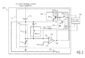
- the PID analog controller 204 includes a feedback (FB) pin 220, resistors, "R FB,1 ,” “R FB,2 ,” that form a feedback divider network 222, an operational transconductance amplifier (OTA) 206, an impedance circuit, "Z feed ,” a capacitor, “C FF ,” CMOS switches, “SW DFT1 ,” “SW DFT2 ,” an NMOS transistor, “MN DFT ,” and a pull-down transistor 224.
- FB feedback
- OTA operational transconductance amplifier
- the PID analog controller 204 is a part of a buck DC/DC converter (not shown).
- the feedback (FB) pin 220 is connected to an output terminal (not shown) of the buck DC/DC converter from which the DC output voltage is outputted and is configured to stabilize the output of the buck DC/DC converter.
- the feedback (FB) pin is connected to a voltage terminal 225, from which the voltage, "V EA,DFT ,” of the PID analog controller 204 is outputted.
- the voltage, "V EA,DFT, " cannot be directly measured at the FB pin 220 because the parasitic impedance of the testing setup circuit will affect the response of the PID analog controller 204. Instead, the voltage, "V EA,DFT, " of the PID analog controller is internally buffered by a DfT interface (not shown).
- the CMOS switches, "SW DFT1 ,” “SW DFT2 ,” the NMOS transistor, “MN DFT ,” and the pull-down transistor 224 form a feedback network or feedback circuit 208.
- the feedback network 208, the OTA 206, the resistors, “R FB,1 ,” “R FB,2 ,” the impedance circuit, "Z feed ,” and the capacitor, “C FF “ form an analog regulation loop 210.
- the NMOS transistor, “MN DFT ,” is connected to a voltage terminal V DDA from which a supply voltage is applied to the feedback network 208, and is configured to operate in saturation as a source follower.
- a control terminal, "dft_off,” is connected to the pull-down transistor.
- the CMOS switch, "SW DFT1 ,” is connected to the pull-down transistor, to the output terminal 230 of the OTA 206, and to the gate terminal 232 of the NMOS transistor, "MN DFT .”
- the CMOS switch, “SW DFT2 ,” is connected in series to the feedforward capacitor, "C FF ,” between the source terminal 234 of the NMOS transistor, “MN DFT ,” and a first input terminal 226 of the OTA 206.
- a second input terminal 228 of the OTA 206 is connected to a reference voltage, "V REF_EA .”
- the first and second input terminals of the OTA 206 are shown in Fig. 2 as being a negative input terminal and a positive input terminal, respectively, in some embodiments, the polarity of the first and second input terminals of the OTA 206 can be reversed, provided that there is still a negative feedback for the OTA.
- the capacitor, "C FF ,” is utilized to improve the transient response of the buck DC/DC converter by adding a zero and a pole to the transfer function in terms of spatial or temporal frequency of the feedback divider network 222 that is formed by the resistors, "R FB,1 ,” “R FB,2 .” This leads to a boost in the gain of the feedback at mid-to-high frequencies, which increases the bandwidth of the PID analog controller, improving the transient response of the buck DC/DC converter.
- the capacitor, "C FF ” can bring the analog regulation loop of the PID controller into an oscillation condition because the phase margin of the analog regulation loop of the PID controller, which is the difference between - 180° and the actual open-loop phase when the open-loop gain reaches 0 dB, can worsen and become negative if the capacitance of the capacitor, "C FF ,” is set in a certain range.
- a switch is in a non-conducting state if the switch is "open,” while a switch is in a conducting state if the switch is “closed.”
- a tester or controller may be used to control the CMOS switches “S WDFT1 ,” “S WDFT2 " via a DfT interface 240.
- the analog regulation loop 210 of the PID analog controller is inactive.
- the CMOS switch, "SW DFT1 ” is open (i.e., non-conducting).
- CMOS switch "SW DFT1 ,” is pulled to the ground by pull-down transistor 224, which closes the NMOS transistor, "MN DFT .”
- the CMOS switch, “SW DFT2 ” is closed in order to electrically connect the capacitor, "C FF ,” to a compensation network formed by the divider network 222, the OTA 206, and the impedance circuit, "Z feed.
- the PID analog controller 204 is in the DfT mode in which the OTA 206 drives a capacitive load and consequently, operates at the intended DC operating point.
- the optimal parameters of the PID analog controller 204 that ensure both stability of the DC/DC converter and intended operation of the PID analog controller 204 in the DfT mode are found using an iterative process. A two-step approach is used in order to test the PID analog controller 206 using the DfT interface 240.
- the capacitor, "C FF ,” is electrically disconnected from the feedback network by opening CMOS switch, "SW DFT2 ,” and at least one DC characteristic of the PID analog controller is tested.
- the PID analog controller 204 is configured as a stable closed-loop system (i.e., in a stable condition) via the DfT interface 240 by closing the CMOS switch, "SW DFT1 ,” releasing the pull-down transistor 224 and opening the CMOS switch, "SW DFT2 .”
- the pull-down transistor is set to a high-impedance state (i.e., the off state) during testing.
- the NMOS transistor, "MN DFT ,” closes the regulation loop 210.
- the PID analog controller works as a stable system and the analog regulation loop 210 of the PID analog controller does not oscillate. In the stable condition, the phase margin of the analog regulation loop 210 of the PID analog controller is larger than 0°, which can be found using an iterative process.
- a DfT analog buffer (not shown) can be employed for buffering the output voltage V EA,DFT .
- a second step the AC performance of the PID analog controller 204 is tested.
- the CMOS switch, "SW DFT2 ” is closed by the DfT interface 240 and the capacitor, "C FF ,” is electrically connected to the feedback network 208.
- the capacitance value of the capacitor, "C FF ” is adjusted to a threshold capacitance value, the phase margin of the PID analog controller's loop, which is the analog regulation loop 210, becomes negative and the analog regulation loop 210 of the PID analog controller 204 is set to an unstable condition and starts to oscillate.
- the optimal capacitance value of the capacitor, "C FF ” is found using an iterative process.
- the AC performance of the PID analog controller can be tested. Defects can be detected by measuring the oscillation signal, which can be digitized by an on-chip window comparator (not shown).
- the feedback network 208 typically only occupies a relatively small circuit area of the PID analog controller 204. Consequently, the area overhead attributed to the feedback network is small. Because both the DC performance and the AC performance of the PID analog controller 204 can be tested at the expense of a small area overhead, the testability of the PID analog controller of the buck DC/DC converter is greatly improved and the product quality is enhanced.
- the PID analog controller 204 enables detection of all bridge defects in the PID analog controller's compensation network. Additionally, the PID analog controller enables testing of the OTA in the intended DC operating point, which improves the test coverage of the OTA. Furthermore, because most defects affecting the performance of the PID analog controller can be detected by examining deviations in the controller's DC and AC parameters, the overall testing coverage of the PID analog controller is improved.
- Figs. 3 , 4a and 4b Examples of stability analysis and transient analysis of the PID analog controller 204 are shown in Figs. 3 , 4a and 4b .
- Fig. 3 depicts an example of a stability analysis of the PID analog controller 204 depicted in Fig. 2 .
- the stability analysis is used to demonstrate the worsening of the phase margin in the frequency domain.
- the upper section of Fig. 3 depicts the magnitude of the loop gain (dB) of the PID analog controller 204 and the lower section of Fig. 3 depicts the phase (deg) of the analog regulation loop 210 of the PID analog controller 204.
- the capacitor, "C FF ” When the analog regulation loop is in a stable condition, the capacitor, "C FF ,” is disconnected from the feedback network 208 and the phase margin of the PID analog controller's loop is positive. When the analog regulation loop is in an unstable condition, the capacitor, “C FF, " is connected to the feedback network 208, adding a zero and a pole to the frequency response of the feedback network, boosting the open-loop gain, and causing the phase margin of the PID analog controller's loop to become negative.
- the curve, "A-1” represents the loop gain of the PID analog controller in a stable condition
- the curve, "B-1” represents the loop gain of the PID analog controller in an unstable condition. In the lower section of Fig.
- the curve, "A-2” represents the phase of the PID analog controller loop in a stable condition and the curve, "B-2,” represents the phase of the PID analog controller loop in an unstable condition.
- the curve, "A-1” the curve, "B-1” has a higher loop gain when the frequency is over 10 5 Hz.
- the curve, "B-2” shows a higher phase shift when the frequency is over 10 5 Hz .
- Figs. 4a and 4b depict examples of a transient analysis of the PID analog controller 204 depicted in Fig. 2 .
- the transient analysis is used to demonstrate the two-step testing approach in the time domain.
- Fig. 4a depicts a full view of a transient voltage response of the PID analog controller 204
- Fig. 4b depicts a detailed view of a specific time period of the transient response of the PID analog controller 204.
- the PID analog controller powers up in the test mode.
- the DC-performance is tested by measuring the voltage "V EA,DFT " as (1 + R FB,1 /R FB,2 )xV REF,EA .
- the capacitor, "C FF, " is disconnected from the feedback network and consequently, the PID analog controller is stable.
- the capacitor, "C FF, " is connected to the feedback network 208, making the PID controller oscillate at a frequency that is related to its transfer function, allowing its AC-performance to be tested. Any fault that causes a deviation in a parameter of the PID analog controller outside an expected range can be detected.
- the voltage response during the first step occurs before time line, "D," which is around 65 microseconds ( ⁇ s ) while the voltage response during the second step occurs after time line, "D.” As shown in Fig.
- the voltage response during the first step is generally stable while the voltage response during the second step oscillates at a certain frequency with the amplitude of the oscillation.
- the oscillation frequency and amplitude are used to measure the state of the analog regulation loop of the PID analog controller. If the oscillation frequency or the amplitude of the oscillation is out of a normal range that is set for the PID analog controller, a fault within the PID analog controller is detected.
- Fig. 4b depicts a detailed view of the voltage response during the second step. As shown in Fig. 4b , the voltage response between 77 ⁇ s and 79.5 ⁇ s oscillates between 0.96V and 1.44V at a frequency of 3.5 Mhz.
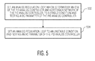
- Fig. 5 is a process flow diagram that illustrates a method for testing a PID analog controller of a DC/DC converter in accordance with an embodiment of the invention.
- an analog regulation loop which is formed by an OTA of the PID analog controller and a feedback network of the PID analog controller, is set to a stable condition and testing a DC parameter of the PID analog controller.
- the analog regulation loop is set to an unstable condition and testing an AC parameter of the PID analog controller
Landscapes
- Engineering & Computer Science (AREA)
- Physics & Mathematics (AREA)
- General Physics & Mathematics (AREA)
- Power Engineering (AREA)
- Electromagnetism (AREA)
- Radar, Positioning & Navigation (AREA)
- Automation & Control Theory (AREA)
- Tests Of Electronic Circuits (AREA)
- Dc-Dc Converters (AREA)
- Feedback Control In General (AREA)
Applications Claiming Priority (1)
| Application Number | Priority Date | Filing Date | Title |
|---|---|---|---|
| US13/705,508 US9091741B2 (en) | 2012-12-05 | 2012-12-05 | Proportional-integral-derivative (PID) analog controller and a method for testing a PID analog controller of a DC/DC converter |
Publications (2)
| Publication Number | Publication Date |
|---|---|
| EP2741408A2 true EP2741408A2 (de) | 2014-06-11 |
| EP2741408A3 EP2741408A3 (de) | 2018-05-16 |
Family
ID=49303795
Family Applications (1)
| Application Number | Title | Priority Date | Filing Date |
|---|---|---|---|
| EP13187114.7A Withdrawn EP2741408A3 (de) | 2012-12-05 | 2013-10-02 | Proportional-integraler Derivat- (PID) Analogregler und Verfahren zum Testen eines analogen PID-Reglers eines Gleichspannungswandlers |
Country Status (2)
| Country | Link |
|---|---|
| US (1) | US9091741B2 (de) |
| EP (1) | EP2741408A3 (de) |
Families Citing this family (15)
| Publication number | Priority date | Publication date | Assignee | Title |
|---|---|---|---|---|
| US9903917B2 (en) * | 2014-10-07 | 2018-02-27 | Texas Instruments Incorporated | Method and circuitry for detecting faults in field oriented controlled permanent magnet synchronous machines |
| US9948173B1 (en) * | 2014-11-18 | 2018-04-17 | The Board Of Trustees Of The University Of Alabama | Systems and methods for short-time fourier transform spectrogram based and sinusoidality based control |
| US10248177B2 (en) | 2015-05-22 | 2019-04-02 | Advanced Micro Devices, Inc. | Droop detection and regulation for processor tiles |
| US9946278B2 (en) | 2015-05-22 | 2018-04-17 | Advanced Micro Devices, Inc. | Droop detection for low-dropout regulator |
| US9991707B2 (en) * | 2015-07-24 | 2018-06-05 | Battelle Memorial Institute | Aggregate Load Controllers and Associated Methods |
| WO2017069900A1 (en) * | 2015-10-21 | 2017-04-27 | Advanced Micro Devices, Inc. | Droop detection and regulation for processor tiles |
| CN108627716B (zh) * | 2017-03-22 | 2021-08-31 | 株洲中车时代电气股份有限公司 | 一种变流器整机全过程检测覆盖率分析方法 |
| KR102586441B1 (ko) * | 2018-06-19 | 2023-10-11 | 주식회사 엘엑스세미콘 | 전원관리집적회로 |
| KR102731056B1 (ko) | 2019-04-25 | 2024-11-15 | 삼성전자주식회사 | 출력 전압의 발진을 검출하는 전력 변환기 |
| CN111181355B (zh) * | 2020-01-19 | 2021-06-01 | 苏州浪潮智能科技有限公司 | 一种调整电源电路输出电压的装置及方法 |
| CN111479350B (zh) * | 2020-04-15 | 2025-01-07 | 上海赫爽太阳能科技有限公司 | 一种放电网络结合igbt控制太阳模拟器闪光波形方法 |
| IT202000013627A1 (it) | 2020-06-08 | 2021-12-08 | St Microelectronics Srl | Un circuito di controllo per un convertitore elettronico, relativo circuito integrato, convertitore elettronico e procedimento |
| DE102020213559B4 (de) * | 2020-10-28 | 2022-05-05 | Infineon Technologies Ag | Bestimmung einer Information über eine Verbindung einer Schaltungskomponente |
| IT202200016299A1 (it) | 2022-08-01 | 2024-02-01 | St Microelectronics Srl | Circuito di controllo per un convertitore elettronico, relativo circuito integrato, convertitore elettronico e procedimento |
| CN116360540B (zh) * | 2023-05-19 | 2023-09-29 | 四川奥库科技有限公司 | 用于芯片测试的电压调节系统及电压调节方法 |
Family Cites Families (8)
| Publication number | Priority date | Publication date | Assignee | Title |
|---|---|---|---|---|
| DK3589081T3 (da) * | 2004-03-15 | 2024-03-18 | Signify North America Corp | Effektstyringfremgangsmåder og -apparat |
| CN101036064A (zh) * | 2004-10-12 | 2007-09-12 | 半导体元件工业有限责任公司 | 测试电源控制器的方法及其结构 |
| TWI312608B (en) * | 2006-08-01 | 2009-07-21 | Ind Tech Res Inst | Dc-dc converter and error amplifier thereof |
| US8487600B2 (en) * | 2007-04-10 | 2013-07-16 | Aleksandar Prodic | Continuous-time digital controller for high-frequency DC-DC converters |
| EP2330735A3 (de) * | 2008-07-18 | 2012-04-04 | Peregrine Semiconductor Corporation | Transkonduktanz-Operationsverstärker |
| US7772904B1 (en) * | 2009-02-16 | 2010-08-10 | Infineon Technologies Ag | Voltage level converter with mixed signal controller |
| US8693228B2 (en) * | 2009-02-19 | 2014-04-08 | Stefan Matan | Power transfer management for local power sources of a grid-tied load |
| CN201698013U (zh) * | 2010-02-01 | 2011-01-05 | 鸿富锦精密工业(深圳)有限公司 | 直流电源测试装置 |
-
2012
- 2012-12-05 US US13/705,508 patent/US9091741B2/en not_active Expired - Fee Related
-
2013
- 2013-10-02 EP EP13187114.7A patent/EP2741408A3/de not_active Withdrawn
Non-Patent Citations (1)
| Title |
|---|
| None |
Also Published As
| Publication number | Publication date |
|---|---|
| EP2741408A3 (de) | 2018-05-16 |
| US20140152339A1 (en) | 2014-06-05 |
| US9091741B2 (en) | 2015-07-28 |
Similar Documents
| Publication | Publication Date | Title |
|---|---|---|
| US9091741B2 (en) | Proportional-integral-derivative (PID) analog controller and a method for testing a PID analog controller of a DC/DC converter | |
| Zhan et al. | An output-capacitor-free adaptively biased low-dropout regulator with subthreshold undershoot-reduction for SoC | |
| JP5987206B2 (ja) | 電圧調整回路機構および関連する動作方法 | |
| EP3071978B1 (de) | Batteriebrennstoffmesser mit fet-segmentsteuerung zur erhöhung der niederstrommessgenauigkeit | |
| US10958160B2 (en) | Feedback scheme for stable LDO regulator operation | |
| US9891643B2 (en) | Circuit to improve load transient behavior of voltage regulators and load switches | |
| CN105634276A (zh) | 线性调节器 | |
| CN113466538B (zh) | 一种负载开关中的小电流检测电路及其检测方法 | |
| CN100538582C (zh) | 电压调节器 | |
| WO2014152901A2 (en) | Ldo and load switch supporting a wide range of load capacitance | |
| JP4630764B2 (ja) | ハイ側のスイッチにおいて正および負のピークインダクタ電流を損失無くセンスする方法及び装置 | |
| TW200941174A (en) | Power management circuit and method of frequency compensation thereof | |
| US9110488B2 (en) | Wide-bandwidth linear regulator | |
| CN114113967A (zh) | 一种源测量单元测试系统及测试方法 | |
| WO2017107267A1 (zh) | 一种反馈控制电路及电源管理模块 | |
| US9755518B2 (en) | Current measurments in switching regulators | |
| CN103777047B (zh) | 阻抗源量程调节设备和方法 | |
| CN109683648B (zh) | 一种ldo电路 | |
| WO2014011490A1 (en) | Method and apparatus for characterizing power supply imepdance for power delivery networks | |
| CN215117303U (zh) | 一种电压产生电路 | |
| CN120831562A (zh) | 一种高可靠性电源芯片电路故障检测系统 | |
| CN118465514B (zh) | 精确测试芯片检流比例及等效阻抗的电路 | |
| CN109725631B (zh) | 一种静态电流测试装置和车辆 | |
| US20200003720A1 (en) | Sensor arrangement for voltammetry | |
| CN111211690A (zh) | 一种电源电路 |
Legal Events
| Date | Code | Title | Description |
|---|---|---|---|
| PUAI | Public reference made under article 153(3) epc to a published international application that has entered the european phase |
Free format text: ORIGINAL CODE: 0009012 |
|
| 17P | Request for examination filed |
Effective date: 20140326 |
|
| AK | Designated contracting states |
Kind code of ref document: A2 Designated state(s): AL AT BE BG CH CY CZ DE DK EE ES FI FR GB GR HR HU IE IS IT LI LT LU LV MC MK MT NL NO PL PT RO RS SE SI SK SM TR |
|
| AX | Request for extension of the european patent |
Extension state: BA ME |
|
| RAP1 | Party data changed (applicant data changed or rights of an application transferred) |
Owner name: NEXPERIA B.V. |
|
| RAP1 | Party data changed (applicant data changed or rights of an application transferred) |
Owner name: NEXPERIA B.V. |
|
| RIC1 | Information provided on ipc code assigned before grant |
Ipc: H02M 1/00 20060101ALI20171222BHEP Ipc: G05F 1/46 20060101ALI20171222BHEP Ipc: H02M 3/00 20060101AFI20171222BHEP Ipc: G01R 31/40 20140101ALI20171222BHEP |
|
| PUAL | Search report despatched |
Free format text: ORIGINAL CODE: 0009013 |
|
| AK | Designated contracting states |
Kind code of ref document: A3 Designated state(s): AL AT BE BG CH CY CZ DE DK EE ES FI FR GB GR HR HU IE IS IT LI LT LU LV MC MK MT NL NO PL PT RO RS SE SI SK SM TR |
|
| AX | Request for extension of the european patent |
Extension state: BA ME |
|
| RIC1 | Information provided on ipc code assigned before grant |
Ipc: G05F 1/46 20060101ALI20180411BHEP Ipc: G01R 31/40 20140101ALI20180411BHEP Ipc: H02M 3/00 20060101AFI20180411BHEP Ipc: H02M 1/00 20060101ALI20180411BHEP |
|
| STAA | Information on the status of an ep patent application or granted ep patent |
Free format text: STATUS: THE APPLICATION IS DEEMED TO BE WITHDRAWN |
|
| 18D | Application deemed to be withdrawn |
Effective date: 20181117 |