EP2741328A1 - Light-emitting device and luminaire - Google Patents
Light-emitting device and luminaire Download PDFInfo
- Publication number
- EP2741328A1 EP2741328A1 EP13182264.5A EP13182264A EP2741328A1 EP 2741328 A1 EP2741328 A1 EP 2741328A1 EP 13182264 A EP13182264 A EP 13182264A EP 2741328 A1 EP2741328 A1 EP 2741328A1
- Authority
- EP
- European Patent Office
- Prior art keywords
- light
- emitting
- metal layer
- layer
- section
- Prior art date
- Legal status (The legal status is an assumption and is not a legal conclusion. Google has not performed a legal analysis and makes no representation as to the accuracy of the status listed.)
- Withdrawn
Links
Images


Classifications
-
- H—ELECTRICITY
- H05—ELECTRIC TECHNIQUES NOT OTHERWISE PROVIDED FOR
- H05K—PRINTED CIRCUITS; CASINGS OR CONSTRUCTIONAL DETAILS OF ELECTRIC APPARATUS; MANUFACTURE OF ASSEMBLAGES OF ELECTRICAL COMPONENTS
- H05K1/00—Printed circuits
- H05K1/02—Details
- H05K1/0201—Thermal arrangements, e.g. for cooling, heating or preventing overheating
- H05K1/0203—Cooling of mounted components
- H05K1/0209—External configuration of printed circuit board adapted for heat dissipation, e.g. lay-out of conductors, coatings
-
- H—ELECTRICITY
- H05—ELECTRIC TECHNIQUES NOT OTHERWISE PROVIDED FOR
- H05K—PRINTED CIRCUITS; CASINGS OR CONSTRUCTIONAL DETAILS OF ELECTRIC APPARATUS; MANUFACTURE OF ASSEMBLAGES OF ELECTRICAL COMPONENTS
- H05K3/00—Apparatus or processes for manufacturing printed circuits
- H05K3/0058—Laminating printed circuit boards onto other substrates, e.g. metallic substrates
- H05K3/0061—Laminating printed circuit boards onto other substrates, e.g. metallic substrates onto a metallic substrate, e.g. a heat sink
-
- H—ELECTRICITY
- H05—ELECTRIC TECHNIQUES NOT OTHERWISE PROVIDED FOR
- H05K—PRINTED CIRCUITS; CASINGS OR CONSTRUCTIONAL DETAILS OF ELECTRIC APPARATUS; MANUFACTURE OF ASSEMBLAGES OF ELECTRICAL COMPONENTS
- H05K3/00—Apparatus or processes for manufacturing printed circuits
- H05K3/22—Secondary treatment of printed circuits
- H05K3/28—Applying non-metallic protective coatings
- H05K3/284—Applying non-metallic protective coatings for encapsulating mounted components
-
- H—ELECTRICITY
- H10—SEMICONDUCTOR DEVICES; ELECTRIC SOLID-STATE DEVICES NOT OTHERWISE PROVIDED FOR
- H10H—INORGANIC LIGHT-EMITTING SEMICONDUCTOR DEVICES HAVING POTENTIAL BARRIERS
- H10H20/00—Individual inorganic light-emitting semiconductor devices having potential barriers, e.g. light-emitting diodes [LED]
- H10H20/80—Constructional details
- H10H20/85—Packages
- H10H20/851—Wavelength conversion means
- H10H20/8514—Wavelength conversion means characterised by their shape, e.g. plate or foil
-
- H—ELECTRICITY
- H10—SEMICONDUCTOR DEVICES; ELECTRIC SOLID-STATE DEVICES NOT OTHERWISE PROVIDED FOR
- H10H—INORGANIC LIGHT-EMITTING SEMICONDUCTOR DEVICES HAVING POTENTIAL BARRIERS
- H10H20/00—Individual inorganic light-emitting semiconductor devices having potential barriers, e.g. light-emitting diodes [LED]
- H10H20/80—Constructional details
- H10H20/85—Packages
- H10H20/858—Means for heat extraction or cooling
- H10H20/8582—Means for heat extraction or cooling characterised by their shape
-
- H—ELECTRICITY
- H10—SEMICONDUCTOR DEVICES; ELECTRIC SOLID-STATE DEVICES NOT OTHERWISE PROVIDED FOR
- H10H—INORGANIC LIGHT-EMITTING SEMICONDUCTOR DEVICES HAVING POTENTIAL BARRIERS
- H10H20/00—Individual inorganic light-emitting semiconductor devices having potential barriers, e.g. light-emitting diodes [LED]
- H10H20/80—Constructional details
- H10H20/85—Packages
- H10H20/858—Means for heat extraction or cooling
- H10H20/8583—Means for heat extraction or cooling not being in contact with the bodies
-
- H—ELECTRICITY
- H10—SEMICONDUCTOR DEVICES; ELECTRIC SOLID-STATE DEVICES NOT OTHERWISE PROVIDED FOR
- H10W—GENERIC PACKAGES, INTERCONNECTIONS, CONNECTORS OR OTHER CONSTRUCTIONAL DETAILS OF DEVICES COVERED BY CLASS H10
- H10W90/00—Package configurations
-
- F—MECHANICAL ENGINEERING; LIGHTING; HEATING; WEAPONS; BLASTING
- F21—LIGHTING
- F21Y—INDEXING SCHEME ASSOCIATED WITH SUBCLASSES F21K, F21L, F21S and F21V, RELATING TO THE FORM OR THE KIND OF THE LIGHT SOURCES OR OF THE COLOUR OF THE LIGHT EMITTED
- F21Y2115/00—Light-generating elements of semiconductor light sources
- F21Y2115/10—Light-emitting diodes [LED]
-
- H—ELECTRICITY
- H05—ELECTRIC TECHNIQUES NOT OTHERWISE PROVIDED FOR
- H05K—PRINTED CIRCUITS; CASINGS OR CONSTRUCTIONAL DETAILS OF ELECTRIC APPARATUS; MANUFACTURE OF ASSEMBLAGES OF ELECTRICAL COMPONENTS
- H05K1/00—Printed circuits
- H05K1/02—Details
- H05K1/03—Use of materials for the substrate
- H05K1/0306—Inorganic insulating substrates, e.g. ceramic, glass
-
- H—ELECTRICITY
- H05—ELECTRIC TECHNIQUES NOT OTHERWISE PROVIDED FOR
- H05K—PRINTED CIRCUITS; CASINGS OR CONSTRUCTIONAL DETAILS OF ELECTRIC APPARATUS; MANUFACTURE OF ASSEMBLAGES OF ELECTRICAL COMPONENTS
- H05K2201/00—Indexing scheme relating to printed circuits covered by H05K1/00
- H05K2201/03—Conductive materials
- H05K2201/0302—Properties and characteristics in general
- H05K2201/0305—Solder used for other purposes than connections between PCB or components, e.g. for filling vias or for programmable patterns
-
- H—ELECTRICITY
- H05—ELECTRIC TECHNIQUES NOT OTHERWISE PROVIDED FOR
- H05K—PRINTED CIRCUITS; CASINGS OR CONSTRUCTIONAL DETAILS OF ELECTRIC APPARATUS; MANUFACTURE OF ASSEMBLAGES OF ELECTRICAL COMPONENTS
- H05K2201/00—Indexing scheme relating to printed circuits covered by H05K1/00
- H05K2201/10—Details of components or other objects attached to or integrated in a printed circuit board
- H05K2201/10007—Types of components
- H05K2201/10106—Light emitting diode [LED]
-
- H—ELECTRICITY
- H10—SEMICONDUCTOR DEVICES; ELECTRIC SOLID-STATE DEVICES NOT OTHERWISE PROVIDED FOR
- H10W—GENERIC PACKAGES, INTERCONNECTIONS, CONNECTORS OR OTHER CONSTRUCTIONAL DETAILS OF DEVICES COVERED BY CLASS H10
- H10W90/00—Package configurations
- H10W90/701—Package configurations characterised by the relative positions of pads or connectors relative to package parts
- H10W90/721—Package configurations characterised by the relative positions of pads or connectors relative to package parts of bump connectors
- H10W90/724—Package configurations characterised by the relative positions of pads or connectors relative to package parts of bump connectors between a chip and a stacked insulating package substrate, interposer or RDL
Definitions
- Embodiments described herein generally relate to a light-emitting device and a luminaire.
- a light-emitting device in which a semiconductor light-emitting element that emits blue light and a phosphor that converts the wavelength of the light are combined to emit white light.
- the light-emitting device can be applied to, for example, a luminaire such as a floodlight. In such an application, a light amount per unit area is high. It is necessary to improve thermal radiation properties.
- a light-emitting device including a light-emitting section, a thermal radiation member, and a heat conduction layer.
- the light-emitting section includes a mounting substrate section and a light-emitting element section.
- the mounting substrate section includes a substrate, a first metal layer, and a second metal layer.
- the substrate includes a first principal plane including a mounting region and a second principal plane on the opposite side of the first principal plane and is insulative.
- the first metal layer is provided on the first principal plane.
- the first metal layer includes a plurality of mounting patterns provided in the mounting region.
- the second metal layer is provided on the second principal plane and electrically insulated from the first metal layer.
- the light-emitting element section includes a plurality of semiconductor light-emitting elements and a wavelength conversion layer.
- the plurality of semiconductor light-emitting elements are provided on the first principal plane.
- Each of the plurality of semiconductor light-emitting elements is electrically connected to any one mounting pattern among the plurality of mounting patterns and another one mounting pattern adjacent to the mounting pattern among the plurality of mounting patterns.
- the wavelength conversion layer covers at least parts of the plurality of semiconductor light-emitting elements, absorbs at least a part of first light emitted from the plurality of semiconductor light-emitting elements, and emits second light having a wavelength different from the wavelength of the first light.
- the luminous exitance of light emitted from the light-emitting element section is equal to or higher than 101 m/mm 2 and equal to or lower than 1001 m/mm 2 .
- the thermal radiation member is opposed to the second principal plane.
- the thermal radiation member has an area equal to or larger than five times the area of the mounting region when projected on the first plane.
- the heat conduction layer is provided between the thermal radiation member and the second metal layer.
- a light-emitting device including a ceramic substrate, a first metal layer, a second metal layer, a third metal layer, a light-emitting section, a first connector, a second connector, and a thermal radiation plate.
- the ceramic substrate includes a first surface and a second surface. The second surface is located on the opposite side of the first surface.
- the ceramic substrate has a pair of first end sides and a pair of second end sides. The pair of second end sides are orthogonal to the first end sides. The pair of second end sides have length equal to or smaller than the length of the first end sides.
- the first metal layer and the second metal layer are formed on the first surface.
- the third metal layer is formed on the second surface.
- One end of the light-emitting section is electrically connected to one end side of the first metal layer.
- the other end of the light-emitting section is electrically connected to one end side of the second metal layer.
- the first connector is provided on the other end side of the first metal layer.
- the second connector is provided on the other end side of the second metal layer.
- the thermal radiation plate is made of metal. The thermal radiation plate is connected to the third metal layer to be opposed to the ceramic substrate via a solder layer.
- the light-emitting section is arranged such that the center of the light-emitting section substantially coincides with the center of the ceramic substrate.
- the center of the light-emitting section, the first connector, and the second connector are arranged on the first axis.
- the first connector and the second connector are arranged to hold the light-emitting section therebetween.
- FIGS. 1A and 1B are schematic diagrams illustrating a light-emitting device and a luminaire according to a first embodiment.
- FIG. 1A is a plan view.
- FIG. 1B is a sectional view illustrating a part of an A1-A2 cross section of FIG. 1A .
- a light-emitting device 110 includes a light-emitting section 40, a thermal radiation member 51, and a heat conduction layer 52.
- the light-emitting section 40 is provided on the thermal radiation member 51.
- the heat conduction layer 52 is provided between the thermal radiation member 51 and the light-emitting section 40.
- the heat conduction layer 52 is provided on the thermal radiation member 51 and the light-emitting section 40 is provided on the heat conduction layer 52.
- one light-emitting section 40 is provided on the thermal radiation member 51.
- a plurality of the light-emitting sections 40 may be provided on one thermal radiation member 51.
- a state in which a component is provided on the other component includes a state in which the component is directly provided on the other component and a state in which another component is inserted between the component and the other component.
- a direction extending from the thermal radiation member 51 to the light-emitting section 40 is referred to as superimposing direction.
- a state in which components are superimposed includes a state in which the components are directly superimposed in contact with each other and a state in which the components are superimposed with another component inserted therebetween.
- the superimposing direction is represented as Z-axis direction.
- One axis direction perpendicular to the Z-axis direction is represented as X-axis direction.
- a direction perpendicular to the Z-axis direction and perpendicular to the X-axis direction is represented as Y-axis direction.
- the thermal radiation member 51 is, for example, tabular.
- the principal plane of the thermal radiation member 51 is, for example, substantially parallel to an X-Y plane.
- a plane shape of the thermal radiation member 51 is, for example, a rectangular shape.
- the thermal radiation member 51 has, for example, first to fourth sides 55a to 55d.
- the second side 55b is separated from the first side 55a.
- the third side 55c connects one end of the first side 55a and one end of the second side 55b.
- the fourth side 55d is separated from the third side 55c and connects the other end of the first side 55a and the other end of the second side 55b.
- a corner portion of the plane shape of the thermal radiation member 51 may be curved.
- the plane shape of the thermal radiation member 51 does not have to be the rectangular shape and is arbitrary.
- a substrate made of metal or the like is used as the thermal radiation member 51. Copper, aluminum, or the like is used as the thermal radiation member 51.
- the light-emitting section 40 emits light. At the same time, the light-emitting section 40 emits heat.
- the heat conduction layer 52 efficiently conducts the heat generated by the light-emitting section 40 to the thermal radiation member 51. Solder or the like is used as the heat conduction layer 52. That is, the heat conduction layer 52 includes the solder. In this case, the heat conduction layer 52 joins the light-emitting section 40 and the thermal radiation member 51.
- an AuSn alloy or the like is used as the heat conduction layer 52.
- Liquid or solid lubricant may be used as the heat conduction layer 52.
- lubricant having conductivity obtained by mixing metal powder of alumina or the like in silicone (conductive grease) or the like may be used as the heat conduction layer 52.
- the light-emitting section 40 includes a mounting substrate section 15 and a light-emitting element section 35.
- the mounting substrate section 15 includes a substrate 10, a first metal layer 11, and a second metal layer 12.
- the substrate 10 includes a first principal plane 10a and a second principal plane 10b.
- the second principal plane 10b is a surface on the opposite side of the first principal plane 10a.
- the thermal radiation member 51 is opposed to the second principal plane 10b of the substrate 10.
- the second principal plane 10b is a surface on the thermal radiation member 51 side.
- a state in which a component is opposed to the other component includes a state in which the components directly face each other and a state in which another component is inserted between the components.
- the first principal plane 10a includes a mounting region 16.
- the mounting region 16 is separated from an outer edge 10r of the first principal plane 10a.
- the mounting region 16 is provided in the center portion of the first principal plane 10a.
- the first principal plane 10a further includes a peripheral region 17.
- the peripheral region 17 is provided around the mounting region 16. An example of the mounting region 16 is explained below.
- the substrate 10 is insulative.
- a ceramic substrate or the like is used as the substrate 10.
- the substrate 10 includes alumina.
- a ceramic substrate containing alumna as a main component is used as the substrate 10.
- the first metal layer 11 is provided on the first principal plane 10a.
- the first metal layer 11 includes a plurality of mounting patterns 11p.
- the plurality of mounting patterns 11p are provided in the mounting region 16. At least any two or more of the plurality of mounting patterns 11p are separated from one another. For example, at least any one of the plurality of mounting patterns 11p is islet. Two of the plurality of mounting patterns 11p are independent from each other.
- the plurality of mounting patterns 11p includes, for example, a first mounting pattern 11pa and a second mounting pattern 11pb.
- Each of the plurality of mounting patters 11p includes, for example, a first mounting portion 11a and a second mounting portion 11b.
- the mounting pattern 11p further includes a third mounting portion 11c.
- the third mounting portion 11c is provided between the first mounting portion 11a and the second mounting portion 11b and connects the first mounting portion 11a and the second mounting portion 11b.
- the first metal layer 11 may further includes a connecting section 44 configured to connect the plurality of mounting patterns 11p one another.
- the first metal layer 11 further includes an electrode section for first connector 45e and an electrode section for second connector 46e.
- the electrode section for first connector 45e is electrically connected to one of the plurality of mounting patterns 11p.
- the electrode section for second connector 46e is electrically connected another one of the plurality of mounting patterns 11p.
- a semiconductor light-emitting element is arranged on a part of one mounting pattern 11p.
- the electrode section for first connector 45e is electrically connected to one of the mounting patterns 11p by the semiconductor light-emitting element.
- a semiconductor light-emitting element is arranged on a part of another one mounting pattern 11p.
- the electrode section for second connector 46e is electrically connected to another one of the mounting patterns 11p.
- the light-emitting section 40 further includes a first connector 45 and a second connector 46 provided on the first principal plane 10a.
- the first connector 45 is electrically connected to the electrode section for first connector 45e.
- the second connector 46 is electrically connected to the electrode section for second connector 46e.
- the first connector 45 is provided on the electrode section for first connector 45e.
- the second connector 46 is provided on the electrode section for second connector 46e.
- the light-emitting element section 35 is arranged between the first connector 45 and the second connector 46. Electric power is supplied to the light-emitting section 40 via the connectors.
- the second metal layer 12 is provided on the second principal plane 10b.
- the second metal layer 12 is electrically insulated from the first metal layer 11. At least a part of the second metal layer 12 overlaps the mounting region 16 when projected on an X-Y plane (a first plane parallel to the first principal plane 10a).
- the first metal layer 11 is provided on the upper surface (the first principal plane 10a) of the substrate 10 and the second metal layer 12 is provided on the lower surface (the second principal plane 10b) of the substrate 10.
- the light-emitting element section 35 is provided on the first principal plane 10a of the substrate 10.
- the light-emitting element section 35 includes a plurality of semiconductor light-emitting elements 20 and a wavelength conversion layer 31.
- the plurality of semiconductor light-emitting elements 20 are provided on the first principal plane 10a. Each of the plurality of semiconductor light-emitting elements 20 emits light.
- the semiconductor light-emitting element 20 includes, for example, a nitride semiconductor.
- the semiconductor light-emitting element 20 includes, for example, In y Al z Ga 1-x-y N (0 ⁇ x ⁇ 1, 0 ⁇ y ⁇ 1, x+y ⁇ 1). However, in this embodiment, a semiconductor light-emitting element is arbitrary.
- the plurality of semiconductor light-emitting elements 20 include, for example, a first semiconductor light-emitting element 20a and a second semiconductor light-emitting element 20b. Each of the plurality of semiconductor light-emitting elements 20 is electrically connected to any one mounting pattern 11p among the plurality of mounting patterns 11p and another one mounting pattern 11p adjacent to the mounting pattern 11p among the plurality of mounting patterns 11p.
- the first semiconductor light-emitting element 20a is electrically connected to the first mounting pattern 11pa and the second mounting pattern 11pb among the plurality of mounting patterns 11p.
- the second mounting pattern 11pb is equivalent to another mounting pattern 11p adjacent to the first mounting pattern 11pa.
- each of the plurality of semiconductor light-emitting elements 20 includes a first semiconductor layer 21 of a first conduction type, a second semiconductor layer 22 of a second conduction type, and a light-emitting layer 23.
- the first conduction type is an n type and the second conduction type is a p type.
- the first conduction type may be the p type and the second conduction type may be the n type.
- the first semiconductor layer 21 includes a first portion (a first semiconductor portion 21a) and a second portion (a second semiconductor portion 21b).
- the second semiconductor portion 21b is parallel to the first semiconductor portion 21a in the direction (e.g., the X-axis direction) crossing the superimposing direction (the Z-axis direction extending from the thermal radiation member 51 to the light-emitting section 40).
- the second semiconductor layer 22 is provided between the second semiconductor portion 21b and the mounting substrate portion 15.
- the light-emitting layer 23 is provided between the second semiconductor portion 21b and the second semiconductor layer 22.
- the semiconductor light-emitting element 20 is, for example, an LED of a flip-chip type.
- the first semiconductor portion 21a of the first semiconductor layer 21 is opposed to the first mounting portion 11a of the mounting pattern 11p.
- the second semiconductor layer 22 is opposed to the second mounting portion 11b of the mounting pattern 11p.
- the first semiconductor portion 21a of the first semiconductor layer 21 is electrically connected to the first mounting portion 11a.
- the second semiconductor layer 22 is electrically connected to the second mounting portion 11b.
- Solder, a gold bump, or the like is used for the connection.
- the connection is performed by, for example, metal melting or solder joining.
- the connection is performed by, for example, an ultrasonic thermo-compression bonding method using a gold bump.
- the light-emitting element section 35 further includes a first joining metal member 21e and a second joining metal member 22e.
- the first joining metal member 21e is provided between the first semiconductor portion 21a and any one of the mounting patterns 11p (e.g., the first mounting portion 11a).
- the second joining metal member 22e is provided between the second semiconductor layer 22 and another mounting pattern 11p (e.g., the second mounting pattern 11pb).
- At least one of the first joining metal member 21e and the second joining metal member 22e includes solder or a gold bump. Consequently, a sectional area (a sectional area cut along the X-Y plane) of each of the first joining metal member 21e and the second joining metal member 22e can be increased. Consequently, it is possible to efficiently transfer heat to the mounting substrate section 15 via the first joining metal member 21e and the second joining metal member 22e, and thereby improving heat radiation properties.
- the wavelength conversion layer 31 covers at least parts of the plurality of semiconductor light-emitting elements 20.
- the wavelength conversion layer 31 absorbs at least a part of light (e.g., first light) emitted from the plurality of semiconductor light-emitting elements 20 and emits second light.
- the wavelength (e.g., peak wavelength) of the second light is different from the wavelength (e.g., peak wavelength) of the first light.
- the wavelength conversion layer 31 includes a plurality of wavelength conversion particles such as phosphors and light transmissive resin in which the plurality of wavelength conversion particles are dispersed.
- the first light includes, for example, blue light.
- the second light includes light having wavelength larger than the wavelength of the first light.
- the second light includes, for example, at least one of yellow light and red light.
- the light-emitting element section 35 further includes a reflecting layer 32.
- the reflecting layer 32 surrounds the wavelength conversion layer 31 in the X-Y plane.
- the reflecting layer 32 includes a plurality of particles such as metal oxides and light transmissive resin in which the particles are dispersed.
- the particles of the metal oxide or the like have light-reflectance.
- the particles of the metal oxide or the like for example, at least one of TiO 2 and Al 2 O 2 can be used. Since the reflecting layer 32 is provided, light emitted from the semiconductor light-emitting elements 20 can be efficiently emitted along a direction (e.g., the upper direction) parallel to the superimposing direction.
- the light-emitting section 40 is, for example, an LED module of a chip-on-board (COB) type.
- COB chip-on-board
- the luminous exitance of light emitted from the light-emitting element section 35 is equal to or higher than 101 m/mm 2 (lumen/square millimeter) and equal to or lower than 1001 m/mm 2 . Desirably, the luminous exitance is equal to or higher than 201 m/mm 2 . That is, in this embodiment, a ratio of the light emitted from the light-emitting element section 35 to a light emission area (luminous exitance) is extremely high. In this specification, the light emission area substantially corresponds to the area of the mounting region 16.
- the light-emitting device 110 is used for, for example, a floodlight.
- the light-emitting device 110 is arranged, for example, on a luminaire member 71.
- the luminaire member 71 is omitted.
- the luminaire member 71 is a part of a luminaire.
- a connecting member for luminaire 53 is provided between the luminaire member 71 and the light-emitting device 110.
- solder or grease is used as the connecting member for luminaire 53.
- the heat of the light-emitting device 110 is conducted to the luminaire member 71 by the connecting member for luminaire 53 and radiated.
- FIGS. 1A and 1B also illustrate the configuration of a luminaire 210 including the light-emitting device 110.
- the luminaire 210 includes the luminaire member 71 and the light-emitting device 110.
- the light-emitting device 110 is provided on the luminaire member 71.
- the luminaire 210 may further include the connecting member for luminaire 53.
- the connecting member for luminaire 53 is provided between the luminaire member 71 and the light-emitting device 110 and set in contact with the thermal radiation member 51 of the light-emitting device 110 and the luminaire member 71.
- the connecting member for luminaire 53 may be included in the light-emitting device 110.
- the thermal radiation member 51 has an area equal to or larger than five times the area of the mounting region 16 when projected on the X-Y plane (the first plane).
- the area of the thermal radiation member 51 is set extremely large with respect to the area of the mounting region 16. Consequently, heat generated in the light-emitting element section 35 provided on the mounting region 16 is spread in an in-plane direction (an in-X-Y plane direction) by the thermal radiation member 51 having the large area.
- the heat spread in the in-plane direction is transmitted to, for example, the luminaire member 71, to which the light-emitting device 110 is attached, and efficiently radiated.
- FIGS. 2A to 2C are schematic plan views illustrating the light-emitting device according to the first embodiment
- FIG. 2A is a plan view illustrating a first principal plane 10a of the substrate 10.
- FIG. 2B is a plan view illustrating a pattern of the first metal layer 11.
- FIG. 2C is a plan view illustrating a pattern of the second metal layer 12.
- the first principal plane 10a includes the mounting region 16 and the peripheral region 17.
- a pattern of the mounting region 16 is substantially circular.
- the center of the mounting region 16 is provided to substantially coincide with the center of the substrate 10.
- the peripheral region 17 is a region around the mounting region 16.
- the area of the peripheral region 17 is larger than the area of the mounting region 16.
- the area of the peripheral region 17 is equal to or larger than four times the area of the mounting region 16.
- the area of the peripheral region 17 is preferably equal to or smaller than nine times the area of the mounting region 16.
- a distance (a shortest distance) between an end (the outer edge 10r) of the first principal plane 10a extending along one direction (e.g., the X-axis direction) parallel to the first principal plane 10a and passing the center of the mounting region 16 and the mounting region 16 is equal to or larger than 1/2 of the width of the mounting region 16 extending along the direction (the X-axis direction) passing the center.
- a distance 17xa (a shortest distance) between the outer edge 10r extending along the X-axis direction and the mounting region 16 is equal to or larger than 1/2 of width 16x of the mounting region 16.
- a distance 17xb (a shortest distance) between the outer edge 10r extending along the X-axis direction and the mounting region 16 is equal to or larger than 1/2 of the width 16x of the mounting region 16.
- a distance 17ya (a shortest distance) between the outer edge 10r extending along the Y-axis direction and the mounting region 16 is equal to or larger than 1/2 of width 16y of the mounting region 16.
- a distance 17yb (a shortest distance) between the outer edge 10r extending along the Y-axis direction and the mounting region 16 is equal to or larger than 1/2 of the width 16y of the mounting region 16.
- the area of the peripheral region 17 is larger than the area of the mounting region 16. Since the area of the peripheral region 17 is set larger than the area of the mounting region 16 in which heat is generated, the generated heat efficiently spreads along the in-plane direction. Consequently, thermal radiation properties are improved.
- the plurality of mounting patterns 11p which are parts of the first metal layer 11, are provided in the mounting region 16.
- the plurality of mounting patterns 11p are provided in a circular region.
- a region where the plurality of mounting patterns 11p are provided is the mounting region 16.
- the mounting region 16 is a region including the plurality of mounting patterns 11p when projected on the X-Y plane. Regions among the plurality of mounting patterns 11p are included in the mounting region 16.
- the inner side of a line connecting, in a shortest distance, the outer edges of the mounting patterns 11p arranged on the outer side among the plurality of mounting patterns 11p is the mounting region 16.
- the plurality of mounting patterns 11p are arranged, for example, in a substantially circular region.
- a substantially circular region including the plurality of mounting patterns 11p may be used as the mounting region 16.
- the mounting region 16 includes a region where the plurality of mounting patterns 11p projected on the X-Y plane are provided.
- the mounting region 16 does not include, when projected on the X-Y plane, a region where the connecting section 44, the electrode section for first connector 45e, and the electrode section for second connector 46e are provided.
- the area is included in the peripheral region 17.
- parts of the plurality of mounting patterns 11p are independent from one another. Independent two mounting patterns 11p adjacent to each other are electrically connected by the semiconductor light-emitting elements 20 arranged on the mounting patterns 11p. Parts of the plurality of semiconductor light-emitting elements 20 are, for example, connected in series. The plurality of semiconductor light-emitting elements 20 connected in series are, for example, arranged side by side along the X-axis direction.
- two of the plurality of mounting patterns 11p are connected by the connecting section 44. Consequently, a group of the plurality of semiconductor light-emitting elements 20 connected in series is further connected.
- a group of the plurality of semiconductor light-emitting elements arranged side by side along the X axis and connected in series are arranged side by side along the Y-axis direction.
- a group of the plurality of semiconductor light-emitting elements arranged connected in series are connected in parallel to each other.
- the mounting pattern 11p is electrically connected to the electrode section for first connector 45e or the electrode section for second connector 46e via a wiring pattern 44c.
- An electric current is supplied to the mounting patter 11p via the first connector 45 provided on the electrode section for first connector 45e and the second connector 46 provided on the electrode section for second connector 46e.
- the electric current is supplied to the semiconductor light-emitting elements 20 and light is generated.
- the area of the second metal layer 12 is designed large.
- the area of the second metal layer 12 is larger than the area of the mounting region 16.
- the area of the second metal layer 12 projected on the X-Y plane (the first plane parallel to the superimposing direction) is equal to or larger than 95% of the area of the second principal plane 10b.
- the efficiency of radiation of heat is improved by setting the area of the second metal layer 12 large.
- a plane pattern of the heat conductive layer 52 substantially extends along a pattern of the second metal layer 12. It is possible to expand the area of the heat conduction layer 52 by setting the area of the second metal layer 12 large. Consequently, it is possible to improve the efficiency of heat conduction via the heat conduction layer 52.
- an outer edge 12r of the second metal layer 12 projected on the X-Y plane (the first plane) is located on the outer side of an outer edge 16r of the mounting region 16.
- the area of the second metal layer 12 projected on the X-Y plane (the first plane) may be smaller than the area of the mounting region 16. In this case, the area of the second metal layer 12 projected on the X-Y plane (the first plane) is still larger than 80% of the area of the mounting region 16. If the area of the second metal layer 12 is smaller than 80% of the area of the mounting region 16, the efficiency of thermal radiation falls.
- FIG. 3 is a graph illustrating the light-emitting device according to the first embodiment.
- FIG. 3 is an example of a change in light emission efficiency of the semiconductor light-emitting elements 20 that occurs when the area of the thermal radiation member 51 is changed.
- the area S1 is an area of the thermal radiation member 51 projected on the X-Y plane (the first plane).
- the area S2 is an area of the mounting region 16 projected on the X-Y plane.
- the ordinate of FIG. 3 indicates light emission efficiency Eff (in an arbitrary unit). The light emission efficiency Eff of the semiconductor light-emitting elements 20 tends to fall when the temperature of the semiconductor light-emitting elements 20 rises.
- the light emission efficiency Eff corresponds to a temperature rise of the semiconductor light-emitting elements 20. That is, when the light emission efficiency Eff is high, the temperature of the semiconductor light-emitting elements 20 is maintained low. When the light emission efficiency Eff is low, the temperature of the semiconductor light-emitting elements 20 rises. In the example illustrated in FIG. 3 , the luminous exitance of light emitted from the light-emitting element section 35 is equal to or higher than about 201 m/mm 2 .
- the second metal layer 12 is provided on the substrate 10. The second metal layer 12 is connected to the thermal radiation member 51 via the heat conduction layer 52.
- the light emission efficiency Eff is low when the ratio Rs of the area S1 of the thermal radiation member 51 to the area S2 of the mounting region 16 is low.
- the light emission efficiency Eff is high when the ratio Rs is high.
- the ratio Rs is lower than 5, the light emission efficiency Eff suddenly falls. This is because, when the area S1 of the thermal radiation member 51 is smaller than five times the area S2 of the mounting region 16, heat generated in the light-emission element section 35 including the semiconductor light-emitting elements 20 and the wavelength conversion layer 31 is not sufficiently radiated in the thermal radiation member 51. Therefore, in this embodiment, the ratio Rs is set to be equal to or higher than 5. That is, the area S1 of the thermal radiation member 51 is set to be equal to or larger than five times the area S2 of the mounting region 16.
- the ratio Rs is desirably equal to or smaller than twenty-two times.
- the tendency illustrated in FIG. 3 that the light emission efficiency Eff suddenly falls when the ratio Rs of the area S1 of the thermal radiation member 51 to the area S2 of the mounting region 16 is low is not conspicuous when the luminous exitance of light emitted from the light-emitting element section 35 is low.
- the ratio Rs is set to be equal to or higher than 5.
- the size of the light-emitting device is preferably small.
- the ratio Rs is set to be equal to or higher than 5 to obtain high light emission efficiency Eff.
- this embodiment has a configuration specially applied to a light-emitting device having high luminous exitance like a floodlight. According to this embodiment, even when the luminous exitance is high, it is possible to provide a light-emitting device with improved thermal radiation properties.
- the area S1 of the thermal radiation member 51 is set to be equal to or larger than five times the area S2 of the mounting region 16.
- the area of the substrate 10 is preferably set to be equal to or larger than five times the area S2 of the mounting region 16. That is, in this embodiment, the area of the peripheral region 17 is set to be equal to or larger than four times the area of the mounting region 16. Consequently, it is possible to obtain high light emission efficiency Eff.
- the second metal layer 12 insulated from the first metal layer 11 is provided on the lower surface of the substrate 10.
- the second metal layer 12 is not, for example, a route of an electric current supplied to the semiconductor light-emitting elements 20.
- the second metal layer 12 is provided to obtain high thermal radiation properties.
- electrodes are provided in both the upper surface and the lower surface of the substrate 10 and the electrodes provided on the lower surface and the electrodes provided on the upper surface are electrically connected by a through-hole that pierces through the substrate 10.
- a semiconductor light-emitting element is connected to the electrodes provided on the upper surface.
- An electric current supplied to the semiconductor light-emitting element is supplied via the electrodes provided on the lower surface.
- the electrodes provided on the lower surface form a route of the electric current supplied to the semiconductor light-emitting element. Therefore, (at least one of) the electrodes provided on the lower surface cannot be set in contact with the thermal radiation member 51 provided on the lower side of the electrodes. Therefore, thermal radiation via the electrodes provided on the lower surface is insufficient.
- Such a configuration is considered to be applicable to a light-emitting device having low luminous exitance (e.g., a light-emitting device having luminous exitance lower than 101 m/mm 2 ).
- a light-emitting device having high luminous exitance e.g., a light-emitting device having luminous exitance equal to or higher than 101 m/mm 2
- thermal radiation becomes insufficient. As a result, sufficient thermal radiation properties are not obtained.
- the configuration in which the second metal layer 12 insulated from the first metal layer 11 is provided on the lower surface of the substrate 10 is specially applied to the light-emitting device having high luminous exitance like a floodlight. Consequently, even when luminous exitance is high, it is possible to improve the thermal radiation properties.
- the heat conductivity of the thermal radiation member 51 is equal to or higher than 300 W/(m ⁇ k) (watt/(meter ⁇ Kelvin)).
- the heat conductivity of the heat conduction layer 52 is equal to or higher than 5 W/(m ⁇ k) and desirably equal to or higher than 20 W/(m ⁇ K).
- Thickness t52 (see FIG. 1B ) of the heat conductance layer 52 extending along the Z-axis direction (the superimposing direction extending from the thermal radiation member 51 to the light-emitting section 40) is equal to or smaller than 10 ⁇ m (micrometers).
- the heat conductivity of the luminaire member 71 is lower than the heat conductivity of the thermal radiation member 51. Since the heat conductivity of the thermal radiation member 51 is set to be equal to or higher than 300 W/(m ⁇ K), it is possible to sufficiently spread heat in the in-plane direction (in the in-X-Y plane direction) to the luminaire member 71. Consequently, the thermal radiation properties are improved.
- Thermal resistance between a portion of highest temperature on an upper surface 35u (see FIG. 1B ) of the light-emitting element section 35 and an edge portion 10ue (see FIG. 1B ) of the first principal plane 10a (the upper surface) of the substrate 10 is equal to or lower than 0.4°C/W (degree/watt).
- Thermal resistance between an edge portion 51r of the thermal radiation member 51 and the edge portion 10ue of the first principal plane 10a (the upper surface) of the substrate 10 is equal to or lower than 0.1°C/W.
- the junction temperature of the semiconductor light-emitting elements 20 falls, it is possible to improve the light emission efficiency. Further, when solder is used as the heat conduction layer 52, it is possible to suppress a warp of the substrate 10 due to a difference in a coefficient of expansion.
- a ratio of a voltage applied to the light-emitting element section 35 to an electric current supplied to the light-emitting element section 35 is equal to or higher than 100 V/A (volt/ampere) and equal to or lower than 1000 V/A. Since the ratio of the voltage to the electric current is set to be equal to or higher than 100 V/A, for example, it is possible to improve conversion efficiency of an inverter included in a lighting device. When the ratio of the voltage to the electric current exceeds 1000 V/A, the ratio is too high and an element is sometimes broken. Therefore, the ratio is not practical.
- FIGS. 4A and 4B are schematic plan views illustrating the light-emitting device according to the first embodiment.
- FIG. 4A illustrates a pattern shape of the mounting patterns 11p.
- FIG. 4B illustrates an arrangement of the semiconductor light-emitting elements 20.
- parts of the plurality of mounting patterns 11p are arranged side by side along the X-axis direction. Further, a group of the plurality of mounting patterns 11p arranged in the X-axis direction is arranged side by side along the Y-axis direction.
- Each of the plurality of mounting patterns 11p includes the first mounting portion 11a, the second mounting portion 11b, and the third mounting portion 11c.
- the third mounting portion 11c is provided between the first mounting portion 11a and the second mounting portion 11b and connects the first mounting portion 11a and the second mounting portion 11b.
- width w3 of the third mounting portion 11c extending along a traverse direction D2 perpendicular to a direction (an extending direction D1) extending from the first mounting portion 11a to the second mounting portion 11b is smaller than width w1 of the first mounting portion 11a extending along the traverse direction D2.
- the width w3 of the third mounting portion 11c extending along the traverse direction D2 is smaller than width w2 of the second mounting portion 11b extending along the traverse direction D2.
- the semiconductor light-emitting elements 20 are arranged on the mounting patterns 11p.
- a part of the semiconductor light-emitting elements 20 is arranged, for example, on a part of the first mounting pattern 11pa.
- Another part of the semiconductor light-emitting elements 20 is arranged, for example, on a part of the second mounting pattern 11pb.
- the first mounting portion 11a is electrically connected to any one of the semiconductor light-emitting elements 20 (e.g., the first semiconductor light-emitting element 20a).
- the second mounting portion 11b is electrically connected to the second semiconductor light-emitting element 20b.
- the second semiconductor light-emitting element 20b is the semiconductor light-emitting element 20 adjacent to the first semiconductor light-emitting element 20a among the plurality of semiconductor light-emitting elements 20.
- the first mounting portion 11a and the second mounting portion 11b of the mounting pattern 11p are covered by the semiconductor light-emitting elements 20.
- the third mounting portion 11c of the mounting pattern 11p is not covered by the semiconductor light-emitting elements 20.
- any one of the mounting patterns 11p includes the first mounting portion 11a joined to any one of the semiconductor light-emitting elements 20 (e.g., the first semiconductor light-emitting element 20a).
- Another mounting pattern 11p includes the second mounting portion 11b joined to any one of the semiconductor light-emitting elements 20 (e.g., the first semiconductor light-emitting element 20a).
- any one of the semiconductor light-emitting elements 20 when projected on the X-Y plane (the first plane), includes a portion 26a further on the outer side than an outer edge 11ar of the first mounting portion 11a and a portion 26b further on the outer side than an outer edge 11br of the second mounting portion 11b.
- width w20 extending along the traverse direction D2 of each of the plurality of semiconductor light-emitting elements 20 is larger than the width w1 of the first mounting portion 11a extending along the traverse direction D2 and larger than the width w2 of the second mounting portion 11b extending along the traverse direction D2.
- each of the plurality of semiconductor light-emitting elements 20 overlaps at least a part of the third mounting portion 11c.
- the first mounting portion 11a and the second mounting portion 11b of the mounting pattern 11p are covered by the semiconductor light-emitting element 20.
- a ceramic substrate mainly containing alumina is used as the substrate 10.
- the light-reflectance of the ceramic substrate is relatively high.
- the reflectance of the surface (e.g., the first principal plane 10a) of the substrate 10 is higher than the reflectance of the surface of each of the plurality of mounting patterns 11p.
- the reflectance of the surface of the mounting pattern 11p is relatively low.
- the semiconductor light-emitting elements 20 Since the first mounting portion 11a and the second mounting portion 11b of the mounting pattern 11p are covered by the semiconductor light-emitting elements 20, an area of the mounting pattern 11p having relatively low reflectance exposed to the surface can be reduced. Therefore, high reflectance can be obtained as a whole. In this configuration, even when solder is used as the first joining metal member 21e and the second joining metal member 22e, the solder less easily spreads to the side surfaces of the semiconductor light-emitting elements 20 when the semiconductor light-emitting elements 20 are mounted. In an LED of the flit-chip type, a semiconductor layer is sometimes exposed to the side surface because of a manufacturing method. By using this configuration, it is possible to suppress a short circuit from being caused by the solder.
- the plurality of semiconductor light-emitting elements 20 are separated from one another. Therefore, in the positions among the plurality of semiconductor light-emitting elements 20, the third mounting portions 11c of the mounting patterns 11p are not covered by the semiconductor light-emitting elements 20.
- the width w3 of the third mounting portion 11c extending along the traverse direction D2 is set smaller than the width w1 of the first mounting portion 11a and smaller than the width w2 of the second mounting portion 11b. Therefore, an exposed area of the substrate 10 having high reflectance can be increased. Consequently, high reflectance can be obtained as a whole.
- average light-reflectance in the mounting region 16 of the mounting substrate section 15 is equal to or higher than 70%. Since the arrangement explained above is adopted, such high light-reflectance can be obtained.
- FIG. 5 is a schematic sectional view illustrating the light-emitting device according to the first embodiment.
- FIG. 5 illustrates a part of the light-emitting section 40.
- the first metal layer 11 includes a copper layer 13a (a Cu layer).
- the metal layer 11 may further include a gold layer 13d (an Au layer).
- the copper layer 13a is provided between the gold layer 13d and the substrate 10.
- the first metal layer 11 further includes a nickel layer 13b (an Ni layer) provided between the copper layer 13a and the gold layer 13d and a palladium layer 13c (a Pd layer) provided between the nickel layer 13b and the gold layer 13d.
- the first metal layer 11 has a superimposed structure of Cu/Ni/Pd/Au.
- the second metal layer 12 includes a copper layer 14a.
- the second metal layer 12 may further include a gold layer 14d.
- the copper layer 14a is provided between the gold layer 14d and the substrate 10.
- the second metal layer 12 further includes a nickel layer 14b provided between the copper layer 14a and the gold layer 14d and a palladium layer 14c provided between the nickel layer 14b and the gold layer 14d.
- the second metal layer 12 has a superimposed structure of Cu/Ni/Pd/Au.
- the second metal layer 12 for example, a material same as the material of the first metal layer 11 can be used. A superimposed structure same as the superimposed structure of the first metal layer 11 can be applied to the second metal layer 12. This makes it easy to form these metal layers.
- the configuration of the second metal layer 12 may be different from the configuration of the first metal layer 11.
- Thickness t11 of the first metal layer 11 is, for example, equal to or larger than 30 ⁇ m and equal to or smaller than 100 ⁇ m and, for example, equal to or larger than 40 ⁇ m and equal to or smaller than 60 ⁇ m.
- Thickness t12 of the second metal layer 12 is, for example, equal to or larger than 30 ⁇ m and equal to or smaller than 100 ⁇ m and, for example, equal to or larger than 40 ⁇ m and equal to or smaller than 60 ⁇ m.
- the copper layer 13a of the first metal layer 11 and the copper layer 14a of the second metal layer 12 can be formed by, for example, electrolytic plating.
- Each of the thickness of the copper layer 13a and the thickness of the copper layer 14a is, for example, equal to or larger than 30 ⁇ m and equal to or smaller than 100 ⁇ m and is, for example, about 50 ⁇ m.
- the nickel layer 13b, the palladium layer 13c, and the gold layer 13d are formed by, for example, electroless plating.
- the nickel layer 14b, the palladium layer 14c, and the gold layer 14d are formed by, for example, electrolytic plating.
- Each of the thickness of the nickel layer 13b and the thickness of the nickel layer 14b is, for example, equal to or larger than 2 ⁇ m and equal to or smaller than 8 ⁇ m and is, for example, about 4.5 ⁇ m.
- Each of the thickness of the palladium layer 13c and the thickness of the palladium layer 14c is, for example, equal to or larger than 0.075 ⁇ m and equal to or smaller than 0.2 ⁇ m and is, for example, about 1 ⁇ m.
- Each of the thickness of the gold layer 13d and the thickness of the gold layer 14d is, for example, equal to or larger than 0.05 ⁇ m and equal to or smaller than 0.2 ⁇ m and is, for example, about 0.1 ⁇ m.
- the first metal layer 11 and at least a part of the second metal layer 12 are formed by electroless plating, it is possible to substantially vertically form the side surfaces of the first metal layer 11 and the side surfaces of the second metal layer 12.
- a side surface 11s of the first metal layer 11 cut along a plane (e.g., a second plane such as a Y-Z plane) perpendicular to the first principal plane 10a can be formed substantially parallel to the superimposing direction (the Z-axis direction).
- An angle ⁇ between the side surface 11s of the first metal layer 11 and the first principal plane 10a is, for example, equal to or larger than 80 degrees and equal to or smaller than 95 degrees.
- the angle ⁇ is more preferably, for example, equal to or larger than 85 degrees.
- the angle ⁇ is small, the area of the lower surface of the mounting pattern 11p is excessively large with respect to an area (e.g., the area of the upper surface) for mounting the mounting pattern 11p, which is a part of the first metal layer 11. Therefore, a ratio of a portion covered by the mounting pattern 11p in the upper surface (the first principal plane 10a) of the substrate 10 is high. Therefore, it is difficult to increase the reflectance of the entire mounting region 16.
- the angle ⁇ between the side surface 11a of the first metal layer 11 and the first principal plane 10a is set to be equal to or larger than 80 degrees and equal to or smaller than 95 degrees, it is possible to reduce the ratio of the portion covered by the mounting pattern 11p in the upper surface (the first principal plane 10a) of the substrate 10. Consequently, it is possible to sufficiently increase the reflectance of the entire mounting region 16. As a result, it is possible to improve the luminous exitance.
- the curvature of a corner portion of the cross section of the first metal layer 11 is relatively high. That is, the curvature radius of the corner portion is small.
- the cross section of the first metal layer 11 is close to a rectangle, i.e., the side surface 11s is close to a vertical.
- the first metal layer 11 further includes an upper surface 11u parallel to the X-Y plane (the first plane).
- the curvature radius of a corner portion 11su connecting the upper surface 11u of the first metal layer 11 and the side surface 11s of the first metal layer 11 is equal to or smaller than 10 ⁇ m.
- the area of the lower surface of the mounting pattern 11p can be reduced with respect to the area (e.g., the area of the upper surface 11u of the mounting pattern 11p) for mounting the mounting pattern 11p.
- the area e.g., the area of the upper surface 11u of the mounting pattern 11p
- a part of the wavelength conversion layer 31 is arranged in a position 11g (a space) between any one of the plurality of semiconductor light-emitting elements 20 and the substrate 10.
- the position 11g is a position between any one of the mounting patterns 11p (e.g., the first mounting pattern 11pa) and another mounting pattern 11p (e.g., the second mounting pattern 11pb). Since a part of the wavelength conversion layer 31 is arranged in the position 11g (the space) as well, it is possible to efficiently convert the first light emitted from the semiconductor light-emitting element 20 into the second light in the wavelength conversion layer 31.
- a wavelength conversion member including transparent resin or another phosphor material may be separately arranged.
- a vacancy including the position 11g may be increased.
- a gap between the semiconductor light-emitting element 20 and the substrate 10 is increased.
- a distance tg between any one of the plurality of semiconductor light-emitting elements 20 and the substrate 10 extending along the Z-axis direction is set relatively long.
- the distance tg is equal to or larger than 1/10 of thickness t20 (height) of the plurality of semiconductor light-emitting elements 20 extending along the Z-axis direction.
- the height (the thickness t20 extending along the Z-axis direction) of the semiconductor light-emitting layer 20 is, for example, equal to or larger than 50 ⁇ m and equal to or smaller than 500 ⁇ m and is, for example, 300 ⁇ m.
- the distance tg is, for example, equal to or larger than 40 ⁇ m and equal to or smaller than 110 ⁇ m and is, for example, 60 ⁇ m. It is possible to increase the distance tg by increasing the thickness t11 of the first metal layer 11.
- thickness t10 of the substrate 10 is, for example, equal to or larger than 0.3 mm and equal to or smaller than 2 mm and is, for example, 0.635 mm.
- the thickness t10 of the substrate 10 is smaller than 0.3 mm, for example, the mechanical strength of the substrate 10 decreases.
- the thickness t10 of the substrate 10 exceeds 2 mm, for example, efficiency of conduction of heat generated by the semiconductor light-emitting elements 20 (the light-emitting element section 35) to the thermal radiation member 51 falls.
- the wavelength conversion layer 31 includes a plurality of wavelength conversion particles 31a such as phosphors and light transmissive resin 31b in which the plurality of wavelength conversion particles 31a are dispersed.
- the wavelength conversion particles 31a absorb at least a part of the first light emitted from the plurality of semiconductor light-emitting elements 20 and emits the second light having wavelength different from the wavelength of the first light.
- FIG. 6 is a schematic sectional view illustrating the light-emitting device according to the first embodiment.
- FIG. 6 is a sectional view equivalent to a cross section taken along line A1-A2 in FIG. 1A .
- the height of the connectors is preferably set to be equal to or smaller than the height of the light-emitting element section 35.
- a distance h45 (height) between the first principal plane 10a of the substrate 10 and an upper surface 45u of the first connector 45 is equal to or smaller than 1.2 times a distance h35 (height) between the first principal plane 10a of the substrate 10 and the upper surface 35u of the light-emitting element section 35.
- the distance h45 is preferably equal to or smaller than 1.1 times the distance h35.
- the distance h45 is more preferably equal to or smaller than the distance h35.
- the distance h45 is excessively large compared with the distance h35 and the upper surface 45u of the first connector 45 is located excessively above the upper surface 35u of the light-emitting element section 35, light (oblique light) emitted from the light-emitting element section 35 is made incident on the first connector 45. The light is absorbed by the first connector 45 and lost. Further, deterioration of the first connector 45 is accelerated by the light. A reduction in the distance h45 and a reduction in the height of the upper surface of the first connector 45 make it easy to suppress the loss of the light and the deterioration of the first connector 45.
- a distance h46 (height) between the first principal surface 10a of the substrate 10 and an upper surface 46u of the second connector 46 is equal to or smaller than 1.2 times the distance h35 (height) between the first principal surface 10a of the substrate 10 and the upper surface 35u of the light-emitting element section 35.
- the distance h46 is preferably equal to or smaller than 1.1 times the distance h35.
- the distance h46 is more preferably equal to or smaller than the distance h35. This makes it easy to suppress a loss of light and deterioration of the second connector 46.
- the connectors are arranged apart from the mounting region 16.
- a distance L1 (a shortest distance parallel to the X-Y plane) between the first connector 45 and the mounting region 16 is equal to or larger than 1/2 of the width 16x of the mounting region 16.
- a distance L2 (a shortest distance parallel to the X-Y plane) between the second connector 46 and the mounting region 16 is equal to or larger than 1/2 of the width 16x of the mounting region 16. Consequently, a degree of light (oblique light), which is emitted from the light-emitting element section 35, made incident on the first connector 45 and the second connector 46 can be reduced. This makes it easy to suppress a loss of light and deterioration of the connectors.
- laser printing is sometimes applied to the substrate 10.
- a two-dimensional barcode is printed by the laser printing.
- the width of a region of the laser printing is preferably set to be equal to or smaller than 1/5 of the thickness t10 of the substrate 10.
- FIG. 7 is a schematic sectional view illustrating another light-emitting device according to the first embodiment.
- another light-emitting device 111 includes the thermal radiation member 51, the heat conduction layer 52, and the plurality of light-emitting sections 40 (e.g., a first light-emitting section 40a and a second light-emitting section 40b).
- the configurations explained above can be applied to each of the plurality of light-emitting sections 40, the thermal radiation member 51, and the heat conduction layer 52.
- FIG. 7 illustrates the configuration of a luminaire 211 according to this embodiment as well.
- the luminaire 211 includes the luminaire member 71 and the light-emitting device 111 provided on the luminaire member 71.
- the plurality of light-emitting section 40 may be provided for one thermal radiation member 51.
- the heat conduction layer 52 is arranged between the plurality of light-emitting sections 40 and the thermal radiation member 51.
- the heat conduction layer 52 can be divided for each of the plurality of light-emitting sections 40 or one heat conduction layer 52 may be provided for the plurality of light-emitting sections 40.
- the heat conduction layer 52 is divided, it can be considered that the heat conduction layer 52 has a plurality of patterns and a plurality of the heat conduction layers 52 are provided.
- a second embodiment relates to the mounting substrate section 15.
- the mounting substrate section 15 includes, for example, the substrate 10 and a conductive layer (e.g., the first metal layer 11) provided on the substrate 10.
- the conductive layer e.g., the first metal layer 11
- the conductive layer includes a superimposed film including the nickel layer 13b, the palladium layer 13c, and the gold layer 13d.
- the nickel layer 13b, the palladium layer 13c, and the gold layer 13d are provided on the copper layer 13a in this order.
- a resist layer may be provided around the conductive layer provided on the substrate 10.
- a silicon material is used as the resist layer.
- a ceramic substrate having high reflectance is used as the substrate 10.
- a plated layer of Ni/Pd/Au is formed on a reflection surface of the substrate 10. Consequently, for example, discoloration is suppressed. As a result, a fall in reflectance can be suppressed. Further, since the silicon material is used as the resist and the ceramic substrate having high reflectance is used, efficiency can be improved.
- a plated layer of Ni/Ag when a plated layer of Ni/Ag is used as a reflection surface of a mounting substrate, discoloration occurs and a luminous flux tends to fall according to the discoloration.
- the discoloration is mainly affected by a sulfurous gas contained in the air.
- a plated layer of Ni/Au when a plated layer of Ni/Au is used, compared with the plated layer of Ni/Ag, total ray reflectance falls.
- a ceramic substrate of Al 2 O 3 or the like can be used as the substrate.
- a metal substrate of Al or the like may be used as the substrate.
- a plated layer of copper (the copper layer 13a) is provided on a principal surface (either the upper surface or the lower surface) of the substrate.
- a superimposed film of Ni/Pd/Au is provided on the plated layer of copper.
- the superimposed film is formed by, for example, an electrolytic plating method or an electroless plating method.
- the total ray reflectance at a wavelength of 460 nm of the surface of the superimposed layer of Ni/Pd/Au is equal to or higher than 35% and equal to or lower than 50%.
- the total ray reflectance is, for example, a ratio of a total reflection luminous flux to a parallel incident luminous flux of a test piece.
- the total ray reflectance is ray reflectance including a diffusion component.
- the total ray reflectance at a wavelength of 460 nm on the surface of the superimposed film of Ni/Pd/Au is equal to or higher than 60% and equal to or lower than 70%.
- the thickness of the Ni layer is equal to or larger than 3 ⁇ m and equal to or smaller than 6 ⁇ m.
- the thickness of the Pd layer is equal to or larger than 0.05 ⁇ m and equal to or smaller than 0.1 ⁇ m.
- the thickness of the Au layer is equal to or larger than 0.05 ⁇ m and equal to or smaller than 3 ⁇ m.
- the total ray reflectance at a wavelength of 460 nm of the substrate is equal to or higher than 85% and equal to or lower than 93%.
- the total ray reflectance at a wavelength of 560 nm of the substrate is equal to or higher than 85% and equal to or lower than 93%.
- the mounting substrate section according to this embodiment can be used for, for example, an LED module.
- the LED module can be used for, for example, a luminaire.
- a third embodiment relates to a COB module (e.g., the light-emitting element section 35).
- the COB module includes, for example, the semiconductor light-emitting element 20 and the wavelength conversion layer 31.
- the semiconductor light-emitting element 20 emits blue light.
- the wavelength conversion layer 31 generates, for example, white visible light using the blue light as excitation light.
- the luminous exitance in the COB module is equal to or higher than 101 m/mm 2 .
- the power consumption of the COB module is equal to or larger than 50W.
- a connector for feeding electricity to the COB module is formed of metal.
- the connector has a unipolar structure.
- two or more connectors e.g., the first connector 45 and the second connector 46 are provided.
- a light emission area (e.g., the area of the mounting region 16) is desirably small.
- the light emission area is reduced and light emission density increases, deterioration due to light of the connectors arranged around the mounting region 16 is intensified. Discoloration or the like sometimes occurs in the connectors.
- resin that causes discoloration is not used for the connectors.
- the connectors are formed of only metal. Consequently, it is possible to suppress discoloration of the connectors.
- a plurality of connectors are provided, one of the connectors is used as a positive electrode, and another connector is used as a negative electrode.
- the first connector 45 and the second connector 46 are arranged to hold the light-emitting element section 35 therebetween. Consequently, the heat of the semiconductor light-emitting element 20, which is a heat source on the first principal plane 10a of the substrate 10, can be spread via the first metal layer 11 in advance. Therefore, the thermal radiation properties are further improved.
- the wavelength conversion layer 31 includes, for example, the plurality of wavelength conversion particles 31a and the light transmissive resin 31b (e.g., a sealing material).
- the plurality of wavelength conversion particles 31a are dispersed in the light transmissive resin 31b.
- the light transmissive resin 31b contains dimethyl silicone as a main component.
- the light-transmittance of the light transmissive resin 31b is equal to or higher than 86%.
- the hardness (Shore A) of the light transmissive resin 31b is equal to or higher than 15 and equal to or lower than 50.
- the Shore A is, for example, a standard in measuring the hardness of general rubber.
- a penetrator a pressing needle or an indenter
- a deformation amount (press-in depth) of the penetrator is measured and converted into a numerical value.
- a durometer a spring-type rubber hardness meter
- a COB module of a light-emitting device in order to obtain high luminous exitance, semiconductor light-emitting elements are mounted on a substrate at high density. Therefore, thermal dissipation is poor. Further, an amount of light made incident on the wavelength conversion layer 31 increases. Therefore, the temperature of the wavelength conversion layer 31 tends to rise.
- silicone is used as light transmissive resin of the wavelength conversion layer 31, the heat conductivity of the silicone is about 0.1°C ⁇ W. Therefore, in a high-power COB module, compared with a small-power COB module, the temperature of the wavelength conversion layer 31 is extremely high. The hardness of the silicone rises according to the temperature.
- the hardness (the Shore A) of the light transmissive resin 31b is set to be equal to or higher than 15 and equal to or lower than 50. Consequently, a crack and peeling can be suppressed.
- This embodiment can include, for example, the light-emitting element section 35 including the semiconductor light-emitting elements 20 configured to emit light having a wavelength equal to or larger than 400 nm and equal to or smaller than 480 nm and the wavelength conversion layer 31 configured to cover the semiconductor light-emitting elements 20.
- the luminous exitance in the light-emitting element section 35 (the COB module) is equal to or higher than 101 m/mm 2 and the power consumption of the light-emitting element section 35 is equal to or higher than 50 W.
- the total light transmittance for a wavelength of 400 nm of the light transmissive resin 31b is equal to or higher than 85%.
- this embodiment it is possible to provide a light-emitting device having luminous exitance adaptable to a narrow angle of a floodlight or the like. Even when temperature rises during lighting, it is possible to reduce stress due to temperature stress and suppress a crack and peeling.
- the light-emitting element section 35 is arranged on the mounting substrate section 15.
- the light-emitting section 35 includes the plurality of semiconductor light-emitting elements 20.
- Each of the plurality of semiconductor light-emitting elements 20 is a square 1 mm on each side.
- the dominant wavelength of the semiconductor light-emitting elements 20 is 455 nm.
- a pitch is 1.6 mm.
- the number of semiconductor light-emitting elements 20 is ninety-six.
- dimethyl silicone having Shore A of 70 and elongation of 70% is used as the light transmissive resin 31b of the wavelength conversion layer 31 of the light-emitting element 35.
- dimethyl silicone having Shore A of 43 and elongation of 150% is used as the light transmissive resin 31b.
- dimethyl silicone having Shore A of 32 and elongation of 200% is used as the light transmissive resin 31b.
- a lighting test is performed at an electric current of 440 mA, a voltage of 144 V, and junction temperature of 130°C. During the lighting test, the temperature on the upper surface of the wavelength conversion layer 31 is equal to or higher than 120°C and equal to or lower than 150°C.
- the Shore A is preferably equal to or lower than 50.
- the Shore A is set to be equal to or higher than 15 and equal to or lower than 50. Consequently, a crack and peeling can be suppressed and workability is high.
- the total light transmittance for a wavelength of 400 nm of the light transmissive resin 31b is set to be equal to or higher than 85%, whereby high light extraction efficiency is obtained.
- the total light reflectance is more preferably equal to or higher than 90%.
- FIG. 8 is a schematic sectional view illustrating a light-emitting device and a luminaire according to a fifth embodiment.
- a luminaire 221 according to this embodiment includes a light-emitting device 121 and the luminaire member 71.
- the luminaire member 71 includes, for example, a base section 72 and a reflecting section 73.
- the base section 72 is tabular.
- the reflecting section 73 is provided along an edge of the base section 72.
- the light-emitting device 121 is provided on the base section 72.
- the reflecting section 73 reflects light LL emitted from the light-emitting device 121.
- the light LL can be efficiently irradiated in a desired direction by the reflecting section 73.
- the base section 72 efficiently radiates heat generated in the light-emitting device 121 while holding the light-emitting device 121.
- the light-emitting device 121 includes the thermal radiation member 51, the heat conduction layer 52, and the plurality of light-emitting sections 40 (e.g., the first light-emitting section 40a and the second light-emitting section 40b).
- An interval among the plurality of light-emitting sections 40 is preferably short. Consequently, the light LL having high intensity is emitted from a narrow region. If the light LL is emitted from a wide region, proper reflection is less easily obtained in the reflecting section 73. It is difficult to perform highly efficient reflection in a desired direction. Therefore, it is preferable to bring a light emission characteristic closer to a point light source such that the light LL is emitted from the narrow region. Consequently, highly efficient reflection in the reflecting section 73 is obtained.
- FIGS. 9A and 9B are schematic diagrams illustrating the light-emitting device and the luminaire according to the fifth embodiment.
- FIG. 9A is a plan view.
- FIG. 9B is a sectional view illustrating an A1-A2 line cross section of FIG. 9A .
- the light-emitting device 121 includes the thermal radiation member 51, the heat conduction layer 52, and the plurality of light-emitting sections 40 (e.g., the first light-emitting section 40a, the second light-emitting section 40b, the third light-emitting section 40c, and the fourth light-emitting section 40d).
- the configurations explained in the first embodiment can be applied to each of the plurality of light-emitting sections 40, the thermal radiation member 51, and the heat conduction layer 52.
- the heat conduction layer 52 is divided for each of the plurality of light-emitting sections 40.
- the second light-emitting section 40b is arranged side by side with the first light-emitting section 40a in a surface parallel to the first principal plane 10a.
- the thermal radiation member 51 includes a substrate of copper and a nickel layer provided on the surface of the substrate.
- the nickel layer is formed by, for example, plating.
- SnAg solder is used as the heat conduction layer 52.
- FIGS. 9A and 9B illustrate the configuration of the luminaire 221 according to this embodiment as well.
- the luminaire 221 includes the luminaire member 71 (e.g., the base section 72) and the light-emitting device 121 provided on the luminaire member 71.
- the first light-emitting section 40a includes the plurality of semiconductor light-emitting elements 20 (the first semiconductor light-emitting element 20a, the second semiconductor light-emitting element 20b, etc.).
- the second light-emitting section 40b includes the plurality of semiconductor light-emitting elements 20 (a third semiconductor light-emitting element 20c, a fourth semiconductor light-emitting element 20d, etc.).
- the first light-emitting section 40a includes a first mounting substrate section 15a.
- the second light-emitting section 40b includes a second mounting substrate section 15b.
- the configuration of the mounting substrate section 15 explained in the first embodiment can be applied to each of the first mounting substrate section 15a and the second mounting substrate section 15b.
- the substrate 10 of one light-emitting section 40 (the first light-emitting section 40a) among the plurality of light-emitting sections 40 includes a first side surface 10sa.
- the first side surface 10sa crosses the first principal plane 10a.
- the substrate 10 of another light-emitting section 40 (the second light-emitting section 40b) among the plurality of light-emitting sections 40 includes a second side surface 10sb.
- the second side surface 10sb crosses the first principal plane 10a and is opposed to the first side surface 10sa.
- the light-emitting device 121 further includes a light reflecting resin layer 60.
- the light reflecting resin layer 60 is light-reflective and insulative.
- the light reflecting resin layer 60 covers at least a part of the first side surface 10sa and covers at least a part of the second side surface 10sb.
- the light reflecting resin layer 60 includes, for example, insulative resin and a plurality of particles dispersed in the insulative resin.
- insulative resin for example, at least one of TiO 2 and Al 2 O 3 is used as the plurality of particles.
- at least any one of silicon resin, epoxy resin, acrylic resin, and polyimide resin is used as the insulative resin.
- the reflectance of the light reflecting resin layer 60 is, for example, equal to or higher than 70%. Consequently, high insulation properties and high reflectance are obtained and light use efficiency is improved.
- the interval among the light-emitting sections 40 it is sometimes preferable to reduce the interval among the light-emitting sections 40.
- the area of the substrate 10 included in each of the plurality of light-emitting sections 40 is reduced.
- the first metal layer 11 provided on the first principal plane 10a and the second metal layer 12 provided on the second principal plane 10b of the substrate 10 areas suitable therefor are necessary.
- the light reflective resin layer 60 is provided among the mounting substrate sections 15 of the plurality of light-emitting sections 40 adjacent to one another.
- the light reflecting resin layer 60 covers at least a part of the first side surface 10sa. Consequently, even when the creepage distance of insulation in the first light-emitting section 40a is reduced, satisfactory insulation properties can be maintained in the first mounting substrate section 15a.
- the light reflecting resin layer 60 covers at least a part of the second side surface 10sb. Consequently, even when the creepage distance of insulation in the second light-emitting section 40b is reduced, satisfactory insulation properties can be maintained in the second mounting substrate section 15b.
- the light reflecting resin layer 60 covers the first side surface 10sa and the second side surface 10sb and covers parts of the first principal plane 10a of the substrate 10 of the one light-emitting section 40 (the first light-emitting section 40a) and parts of the first principal plane 10a of the substrate 10 of the other light-emitting section 40 (the second light-emitting section 40b).
- the light reflecting resin layer 60 covers parts of the first metal layer 11 of the first light-emitting section 40a and parts of the first metal layer 11 of the second light-emitting section 40b. Consequently, deterioration in the insulation properties is further suppressed.
- the light reflecting resin layer 60 covers the side surfaces of the first metal layer 11 of the first light-emitting section 40a and the side surfaces of the first metal layer 11 of the second light-emitting section 40b. Consequently, insulation properties between the side surfaces of the first metal layer 11 of the first light-emitting section 40a and the side surfaces of the first metal layer 11 of the second light-emitting section 40b can be improved.
- the light reflecting resin layer 60 covers the side surfaces of the second metal layer 12 of the first light-emitting section 40a and the side surfaces of the second metal layer 12 of the second light-emitting section 40b. Consequently, insulation properties between the side surfaces of the second metal layer 12 of the first light-emitting section 40a and the side surfaces of the second metal layer 12 of the second light-emitting section 40b can be improved.
- the insulation properties between the side surfaces can be improved.
- parts of the light reflecting resin layer 60 is arranged between the substrate 10 of the first mounting substrate section 15a of the first light-emitting section 40a and the thermal radiation member 51. Further, parts of the light reflecting resin layer 60 is arranged between the substrate 10 of the second mounting substrate section 15b of the second light-emitting section 40b and the thermal radiation member 51. The light reflecting resin layer 60 is filled in a space between the first mounting substrate section 15a and the second mounting substrate section 15b. Consequently, the insulation properties can be further improved.
- the light reflecting resin layer 60 covers the outer edges of the substrates 10 included in the plurality of light-emitting sections 40. Consequently, the light use efficiency can be improved.
- a distance g1 between the first side surface 10sa of the substrate 10 of the first light-emitting section 40a and the second side surface 10sb of the substrate 10 of the second light-emitting section 40b is equal to or larger than 0.5 millimeter (mm) and equal to or smaller than 5 millimeters (mm).
- the distance g1 is preferably equal to or smaller than 1 mm.
- the wavelength conversion layer 31 includes a first wavelength conversion film 31p and a second wavelength conversion film 31q.
- the first wavelength conversion film 31p covers the side surfaces of the semiconductor light-emitting elements 20.
- the second wavelength conversion film 31q covers the upper surfaces of the semiconductor light-emitting elements 20 and is provided on the first wavelength conversion film 31p.
- the first wavelength conversion film 31p emits, for example, red light.
- the second wavelength conversion film 31q emits, for example, yellow light.
- FIGS. 10A to 10D are schematic sectional views illustrating other light-emitting devices and other luminaires according to the fifth embodiment.
- the luminaire member 71 is omitted.
- the configuration explained concerning the first embodiment or the configuration explained concerning the luminaire 221 can be applied to the luminaire member 71 in these examples.
- the light reflecting resin layer 60 covers the first side surface 10sa and the second side surface 10sb. Further, the light reflecting resin layer 60 covers parts of the principal plane 10a of the substrate 10 of the first light-emitting section 40a and parts of the first principal plane 10a of the substrate 10 of the second light-emitting section 40b.
- the light reflecting resin layer 60 is separated from the first metal layer 11 and separated from the second metal layer 12. A part of the light reflecting resin layer 60 is arranged between the substrate 10 of the first mounting substrate section 15a and the thermal radiation member 51. Further, a part of the light reflecting resin layer 60 is arranged between the substrate 10 of the second mounting substrate section 15b and the thermal radiation member 51.
- the light reflecting resin layer 60 covers a part of the first metal layer 11 and is in contact with a part of the second metal layer 12. A part of the light reflecting resin layer 60 is arranged between the substrate 10 of the first mounting substrate section 15a and the thermal radiation member 51. A part of the light reflecting resin layer 60 is arranged between the substrate 10 of the second mounting substrate section 15b and the thermal radiation member 51.
- the light reflecting resin layer 60 is separated from the first metal layer 11 and separated from the second metal layer 12.
- the light reflecting resin layer 60 is not arranged between the substrate 10 of the first mounting substrate section 15a and the thermal radiation member 51 and between the substrate 10 of the second mounting substrate section 15b and the thermal radiation member 51.
- the light reflecting resin layer 60 covers a part of the first metal layer 11 and covers a part of the second metal layer 12.
- the light reflecting resin layer 60 is in contact with the reflecting layer 32.
- a part of the light reflecting resin layer 60 is arranged between the substrate 10 of the first mounting substrate section 15a and the thermal radiation member 51.
- a part of the light reflecting resin layer 60 is arranged between the substrate 10 of the second mounting substrate section 15b and the thermal radiation member 51.
- the light reflecting resin layer 60 is filled in the space between the first mounting substrate section 15a and the second mounting substrate section 15b. Consequently, higher insulation properties and higher reflectance can be obtained.
- FIGS. 11A and 11B are schematic diagrams illustrating the light-emitting device and the luminaire according to the fifth embodiment.
- FIG. 11A are plan view.
- FIG. 11B is an A1-A2 line sectional view of FIG. 11A .
- the thermal radiation member 51 has first to fourth sides 55a to 55d.
- the first side 55a extends along the X-axis direction.
- the second side 55b is separated from the first side 55a and extends along the X-axis direction.
- the third side 55c connects one end of the first side 55a and one end of the second side 55b.
- the fourth side 55d is separated from the third side 55c and connects the other end of the first side 55a and the other end of the second side 55b.
- each of the length of the first side 55a and the length of the second side 55b is larger than each of the length of the third side 55c and the length of the fourth side 55d.
- the thermal radiation member 51 may be warped.
- the thermal radiation member 51 and the light-emitting section 40 are joined at high temperature.
- the thermal radiation member 51 is sometimes warped according to a difference in a coefficient of thermal expansion.
- the length of the region where the mounting substrate section 15 is provided is length L01 (mm) of a sum of length La (mm) of one mounting substrate section 15, length Lb (mm) of another mounting substrate section 15, and length Lc (mm) of a space between the mounting substrate sections 15.
- the length L01 is La+Lb+Lc.
- Warp C51 of the thermal radiation member 51 is a difference between positions in the Z-axis direction of the ends of the region of the thermal radiation member 51.
- the warp C51 (mm) of the thermal radiation member 51 is a distance in the Z-axis direction between the end of the region on the lower surface of the thermal radiation member 51 and the center of the lower surface of the thermal radiation member 51.
- the warp C51 of the thermal radiation member 51 may be a distance in the Z-axis direction between the end of the region on the upper surface of the thermal radiation member 51 and the center of the upper surface of the thermal radiation member 51.
- the warp C51 of the thermal radiation member 51 depends on the size of the region where the mounting substrate section 15 is provided.
- Relative warp RC1 is represented as C51/L01.
- the thermal radiation member 51 has thickness t51 (mm).
- the warp of the thermal radiation member 51 depends on the thickness t51 of the thermal radiation member 51.
- Relative thickness RT1 is represented as t51/L01.
- FIG. 12 is a graph illustrating a characteristic of the light-emitting device and the luminaire according to the fifth embodiment.
- FIG. 12 illustrates a simulation result of warp at 25°C obtained after the thermal radiation member 51 and the light-emitting section 40 are joined at 217°C.
- the thermal radiation member 51 and the light-emitting section 40 are joined by the heat conduction layer 52 (e.g., solder).
- the abscissa of FIG. 12 indicates the relative thickness RT1 of the thermal radiation member 51 (a heat spreader) and the ordinate indicates the relative warp RC1.
- the length L01 of the region where the mounting substrate section 15 is provided in the thermal radiation member 51 is 50 mm.
- the thickness t51 of the thermal radiation member 51 is 3 mm.
- the thickness t51 of the thermal radiation member 51 is 6 mm.
- the warp C51 is 0.2 mm.
- the warp C51 is preferably set to be equal to or smaller than 0.2 mm. Consequently, for example, highly efficient reflection in the reflecting section 73 can be obtained.
- the relative warp RC1 is preferably equal to or smaller than 0.004. Consequently, high efficiency by high reflection can be obtained.
- the relative thickness RT1 is preferably 0.06.
- the relative thickness RT1 may be equal to or smaller than 0.12.
- the relative thickness RT1 exceeds 0.12, a material use amount of the thermal radiation member 51 excessively increases.
- the relative thickness RT1 is preferably equal to or larger than 0.06 and equal to or smaller than 0.12. That is, the thickness of the thermal radiation member 51 is preferably equal to or larger than 0.6 times and equal to smaller than 0.12 times the length L01 of the region where the mounting substrate section 15 is provided in the thermal radiation member 51.
- an interval among the COB modules is set to be equal to or larger than a fixed interval. Therefore, the size of the LED module increases and the size of a reflecting mirror and an external size increase. In gaps formed among the COB modules, reflectance is low. Therefore, a reflection loss occurs.
- the area of a light-emitting region is small and light emission density is high in order to satisfy a luminous intensity distribution characteristic.
- the temperature in the center of the light-emitting region further rises.
- fluctuation in temperature sometimes occurs in each of the plurality of COB modules.
- a heat spreader and a plurality of COB modules are combined and, for example, white insulating resin (the light reflecting resin layer 60) is provided in regions among the plurality of COB modules. Consequently, for example, a creepage distance of insulation of a wiring substrate can be reduced. As a result, the size of the light-emitting device can be reduced.
- the light-emitting device can be reduced in size.
- solder is used as the heat conduction layer 52. Consequently, for example, the thermal radiation properties can be improved.
- FIGS. 13A to 13F are schematic sectional views illustrating a light-emitting device and a luminaire according to a sixth embodiment.
- FIG. 13A is a plan view of a light-emitting device 131 and a luminaire 231 according to this embodiment.
- FIG. 13B is a plan view of the thermal radiation member 51 included in the light-emitting device 131.
- FIG. 13C is a plan view of the mounting substrate section 15 included in the light-emitting device 131.
- FIGS. 13D, 13E, and 13F are respectively an A1-A2 line sectional view, an A3-A4 line sectional view, and an A5-A6 line sectional view of FIG. 13A .
- the luminaire 231 includes the light-emitting device 131 and the luminaire member 71.
- the light-emitting device 131 includes the thermal radiation member 51, the heat conduction layer 52, and the light-emitting section 40.
- the ratio Rs is set to be equal to or higher than 5, even when the luminous exitance is as high as equal to or higher than 101 m/mm 2 and equal to or lower than 1001 m/mm 2 , it is possible to provide a light-emitting device with improved thermal radiation properties.
- a first surface (an upper surface 51u) of the thermal radiation member 51 opposed to the second principal plane 10b has irregularities 51p.
- the irregularities 51p of the first surface include a plurality of first groves 51pa.
- the plurality of first grooves 51pa extend, for example, in the X-axis direction (e.g., a first direction parallel to the second principal plane 10b).
- the irregularities 51p of the first surface (the upper surface 51u) further include a plurality of second grooves 51pb.
- the plurality of second grooves 51pb extend, for example, in the Y-axis direction (e.g., parallel to the second principal plane 10b and crossing the first direction).
- the second direction is perpendicular to the first direction.
- an angle between the first direction and the second direction is arbitrary.
- an outer edge 51pe formed when a region 51pr, where the irregularities 51p are provided, in the first surface (the upper surface 51u) is projected on the second principal plane 10b is located on the outer side of an outer edge formed when the substrate 10 is projected on the second principal plane 10b (e.g., the outer edge 10r of the first principal plane 10a).
- a second surface (a lower surface 121) of the second metal layer 12 opposed to the thermal radiation member 51 has irregularities 12p.
- the irregularities 12p of the second surface (the lower surface 121) include a plurality of third grooves 12pa.
- the plurality of third grooves 12pa extend, for example, in the X-axis direction (e.g., a third direction parallel to the second principal plane 10b).
- the irregularities 12p of the second surface (the lower surface 121) further includes a plurality of fourth grooves 12pb.
- the plurality of fourth grooves 12pb extend, for example, in the Y-axis direction (e.g., a fourth direction parallel to the second principal plane 10b and crossing the third direction).
- the fourth direction is perpendicular to the third direction.
- an angle between the third direction and the fourth direction is arbitrary.
- An angle between the third direction and the first direction, an angle between the third direction and the second direction, an angle between the fourth direction and the first direction, and an angle between the fourth direction and the second direction are arbitrary.
- the irregularities 51p may include, for example, a plurality of independent convex portions and concave portions.
- the irregularities 51p may include, for example, a plurality of independent concave portions and convex portions.
- the irregularities 12p may include, for example, a plurality of independent convex portions and concave portions.
- the irregularities 12p may include, for example, a plurality of independent concave portions and convex portions.
- At least one of the irregularities 51p of the thermal radiation member 51 and the irregularities 12p of the second metal layer 12 may be provided.
- the heat conduction layer 52 (e.g., solder) is filled in the concave portions of the irregularities 51p and the concave portions of the irregularities 12p. Since the irregularities are provided, stress is further reduced.
- heat is generated in the light-emitting section 40.
- light emission efficiency (Im/W) in the semiconductor light-emitting elements 20 is reduced by the generated heat.
- the temperature of the light-emitting device e.g., the temperature of the semiconductor light-emitting elements 20
- the temperature of the light-emitting device sometimes rises to be higher than a specification value of an environmental temperature of the light-emitting device.
- the thermal radiation properties for example, there is a structure in which the rear surface of a COB and a thermal radiation plate (the thermal radiation member 51) are joined by solder (the heat conduction layer 52).
- solder the heat conduction layer 52.
- stress is applied to solder according to a difference in a coefficient of thermal expansion among the COB, the thermal radiation plate, and the solder.
- a crack occurs in the solder and reliability falls.
- satisfactory solder joining is less easily obtained.
- a strain that occurs in a joined portion remains large. Therefore, when the COB or the thermal radiation plate warps, the strain concentrates and a crack tends to occur from a portion on which the strain concentrates.
- the irregularities 51p of the thermal radiation member 51 and the irregularities 12p of the second metal layer 12 are provided. Therefore, stress that occurs in the solder (the heat conduction layer 52) is reduced and a strain can be reduced. For example, stress in the X-Y plane is reduced by at least one of the irregularities 51p and the irregularities 12p. Consequently, the reliability can be improved.
- the irregularities 51p are provided, a contact area of the thermal radiation member 51 and the heat conduction layer 52 (e.g., the solder) expands. Since the irregularities 12p are provided, a contact area of the second metal layer 12 and the heat conduction layer 52 (e.g., the solder) expands. Consequently, the thermal radiation properties are improved.
- FIGS. 14A to 14G are schematic sectional views illustrating the light-emitting device according to the sixth embodiment.
- the figures are sectional views of the thermal radiation member 51 according to this embodiment taken along a plane including the Z-axis direction.
- the irregularities 51p provided on the upper surface 51u of the thermal radiation member 51 include a concave portion 51pd.
- the concave portion 51pd includes a bottom surface portion (a thermal radiation member bottom surface portion 51qb) and a side surface portion (a thermal radiation member side surface portion 51qa).
- the side surface portion (the thermal radiation member side surface portion 51qa) crosses the second principal plane 10b (i.e., the X-Y plane).
- the cross section of the thermal radiation member 51 includes two thermal radiation member side surface portions 51qa.
- the cross section of a portion where the two thermal radiation member side surface portions 51qa cross has a triangular shape.
- a convex portion 51pp of the upper surface 51u of the thermal radiation member 51 has a planar shape substantially parallel to the upper surface 51u of the thermal radiation member 51.
- the cross section of the convex portion 51pp of the upper surface 51u of the thermal radiation member 51 has a triangular shape.
- the concave portion 51pd of the thermal radiation member 51 includes the bottom surface portion (the thermal radiation member bottom surface portion 51qb) and the side surface portion (the thermal radiation member side surface portion 51qa).
- the thermal radiation member bottom surface portion 51qb has a planar shape substantially parallel to the X-Y plane.
- the convex portion 51pp of the upper surface 51u of the thermal radiation member 51 has a planar shape substantially parallel to the X-Y plane.
- the cross section of the convex portion 51pp of the upper surface 51u of the thermal radiation member 51 has a triangular shape.
- the concave portion 51pd of the thermal radiation member 51 includes a corner portion (a thermal radiation member corner portion 51qc) in addition to the bottom surface portion (the thermal radiation member bottom surface portion 51qc) and the side surface portion (the thermal radiation member side surface portion 51qa).
- the thermal radiation member corner portion 51qc connects the thermal radiation member bottom portion 51qb and the thermal radiation member side surface portion 51qa and has a curved surface shape.
- the convex portion 51pp of the upper surface 51u of the thermal radiation member 51 has a planar shape substantially parallel to the X-Y plane.
- the convex portion 51pp of the upper surface 51u of the thermal radiation member 51 has a curved surface shape.
- the convex portion 55pp of the upper surface 51u of the thermal radiation member 51 has a planar shape substantially parallel to the X-Y plane.
- the thermal radiation member bottom surface section 51qb has a planar shape substantially parallel to the X-Y plane.
- a thermal radiation member corner portion 51qc having a curved surface shape.
- an edge portion (a corner portion) of the concave portion 51pd e.g., a groove
- the edge portion has a non-curved surface shape
- a crack starts from the edge portion and a crack tends to occur. Since the edge portion is formed in a curved surface shape, it is possible to further suppress occurrence of a crack.
- FIGS. 15A to 15G are schematic sectional views illustrating the light-emitting device according to the sixth embodiment.
- the irregularities 12p provided on the lower surface 121 of the second metal layer 12 includes the concave portion 12pd.
- the concave portion 12pd includes the bottom surface portion (the second metal layer bottom surface portion 12qb) and the side surface portion (the second metal layer side portion 12qa).
- the side surface portion (the second metal layer side surface portion 12qa) crosses the second principal plane 10b (i.e., the X-Y plane).
- the cross section of the second metal layer 12 includes two second metal layer side surface portions 12qa. A portion where the two second metal layer side surface portions 12qa cross (the second metal layer bottom surface portion 12qb) has a triangular shape.
- the convex portion 12pp of the lower surface 121 of the second metal layer 12 has a planar shape substantially parallel to the X-Y plane.
- the cross section of the convex portion 12pp of the lower surface 121 of the second metal layer 12 has a triangular shape.
- the concave portion 12pd of the second metal layer 12 includes the bottom surface portion (the second metal layer bottom surface portion 12qb) and the side surface portion (the second metal layer side surface portion 12qa).
- the second metal layer bottom surface portion 12qb has a planar shape substantially parallel to the X-Y plane.
- the convex portion 12pp of the lower surface 121 of the second metal layer 12 has a planar shape substantially parallel to the X-Y plane.
- the cross section of the convex portion 12pp of the lower surface 121 of the second metal layer 12 has a triangular shape.
- the concave portion 12pd of the second metal layer 12 includes a corner portion (a second metal layer corner portion 12qc) in addition to the bottom surface portion (the second metal layer bottom surface portion 12qb) and the side surface portion (the second metal layer side surface portion 12qa).
- the second metal layer corner portion 12qc connects the second metal layer bottom surface portion 12qb and the second metal layer side surface portion 12qa and has a curved surface shape.
- the convex portion 12pp of the lower surface 121 of the second metal layer 12 has a planar shape substantially parallel to the X-Y plane.
- the convex portion 12pp of the bottom surface 121 of the second metal layer 12 has a curved surface shape.
- the convex portion 12pp of the bottom surface 121 of the second metal layer 12 has a planar shape substantially parallel to the X-Y plane and the second metal layer bottom surface portion 12qb has a planar shape substantially parallel to the X-Y plane.
- the second metal layer corner portion 12qc having a curved surface shape.
- an edge portion (a corner portion) of the concave portion 12pd e.g., a groove
- the shape of the concave portion (e.g., the groove) (a sectional shape of the concave portion cut along the plane including the Z-axis direction) can be, for example, a triangular shape, a trapezoidal shape, or a circular shape (an elliptical shape).
- the shape is the triangular shape or the trapezoidal shape, it is preferable to form the corner portion in a curved surface shape.
- Depth d51 of the irregularities 51p provided on the first surface (the upper surface 51u) of the thermal radiation member 51 is preferably equal to or smaller than 1/10 times the thickness t51 of the thermal radiation member 51 (see FIG. 14G ). Since the depth d51 is set to be equal to or smaller than 1/10 times the thickness t51, for example, it is possible to suppress generation of a void in the solder (the heat conduction layer 52). Further, it is possible to suppress an amount of use of the solder and an increase in costs. When a higher effect is demanded, the depth d51 is desirably equal to or smaller than 1/20 times the thickness t51. The depth d51 is preferably equal to or larger than 1/1000 times the thickness t51 of the thermal radiation member 51. Consequently, it is possible to effectively suppress stress. Improvement of the thermal radiation properties through an increase in the contact area can be effectively obtained.
- depth d12 of the irregularities 12p provided on the second surface (the lower surface 121) of the second metal layer 12 is preferably equal to or smaller than 1/2 times the thickness t12 of the second metal layer 12 (see FIG. 15G ). Since the depth d12 is set to be equal to or smaller than 1/2 times the thickness t12, for example, it is possible to suppress generation of a void in the solder (the heat conduction layer 52). Further, it is possible to suppress an amount of use of the solder and suppress an increase in costs.
- the depth d12 is preferably equal to or larger than 1/100 times the thickness t12 of the second metal layer 12. Consequently, it is possible to effectively suppress stress. Improvement of the thermal radiation properties through an increase in the contact area can be effectively obtained.
- a groove pitch is preferably equal to or larger than two times a groove depth.
- a pitch of a plurality of the concave portions 51pd of the thermal radiation member 51 is preferably equal to or larger than two times the depth of the concave portion 51pd.
- the distance between bottom surface portions (the thermal radiation member bottom surface portions 51qb) of the plurality of concave portions 51pd adjacent to each other is preferably equal to or larger than two times the distance along the Z-axis direction between the convex portion 51pp of the concave portion 52pd and the bottom surface portion (the thermal radiation member bottom surface portion 51pd). Consequently, the shape of the concave portion 51pd (the shape of the groove) is easily stabilized.
- the pitch is more preferably equal to or larger than ten times the depth. Consequently, the shape of the concave portion (the groove) is easily equalized.
- a pitch of a plurality of the concave portions 12pd of the second metal layer 12 is preferably equal to or larger than two times the depth of the concave portion 12pd.
- the distance between bottom surface portions (the second metal layer bottom surface portions 12qb) of the plurality of concave portions 12pd adjacent to each other is preferably equal to or larger than two times the distance along the Z-axis direction between the convex portion 12pp of the concave portion 12pd and the bottom surface portion (the second metal layer bottom surface portion 12pb). Consequently, the shape of the concave portion 12pd (the shape of the groove) is easily stabilized.
- the pitch is more preferably equal to or larger than ten times the depth. Consequently, the shape of the concave portion (the groove) is easily equalized.
- the distance between the grooves is preferably equal to or larger than the depth of the groove.
- the distance between the plurality of concave portions 51pd of the thermal radiation member 51 is preferably equal to or larger than two times the depth of the concave portion 51pd.
- the width (the distance in the direction perpendicular to the Z-axis direction) of the convex portions 51pp of the plurality of concave portions 51pd adjacent to each other is preferably equal to or larger than the distance along the Z-axis direction between the convex portion 51pp of the concave portion 52pd and the bottom surface portion (the thermal radiation member bottom surface portion 51pb). Consequently, a void in the concave portion 51pd (a void generated in the solder) is suppressed. When the distance between the grooves is excessively small, a void tends to remain.
- the distance between the plurality of concave portions 12pd of the second metal layer 12 is preferably equal to or larger than the depth of the concave portion 12pd.
- the width (the distance in the direction perpendicular to the Z-axis direction) of the convex portions 12pp of the plurality of concave portions 12pd adjacent to each other is preferably equal to or larger than the distance along the Z-axis direction between the convex portion 12pp of the concave portion 12pd and the bottom surface portion (the second metal layer bottom surface portion 12pb). Consequently, a void in the concave portion 12pd is suppressed. When the distance between the grooves is excessively small, a void tends to remain.
- a ceramic substrate is used as the substrate 10. Consequently, high heat conductivity and high insulation properties are obtained.
- Solder is used as the heat conduction layer 52. Consequently, high heat conductively is obtained.
- a copper layer is used as the second metal layer 12. Consequently, even when the solder is used as the heat conduction layer 52, satisfactory joining is obtained.
- a selection range for a material of the solder is widened and a condition range for a joining process is expanded.
- aluminum may be used as the second metal layer 12. In this case, the material of the solder tends to be limited and the condition for the joining process tends to be limited.
- the heat conductivity of copper is higher than the heat conductivity of aluminum. Since the copper layer is used as the second metal layer 12, higher thermal radiation properties can be obtained.
- the outer edge 51pe formed when the region 51pr, where the irregularities 51p are provided, in the first surface (the upper surface 51u) is projected on the second principal plane 10b is preferably located on the outer side of an outer edge formed when the light-emitting region is projected on the second principal plane 10b. Consequently, an effect of stress reduction can be obtained.
- the region 51pr is more desirably located on the outer side of an outer edge formed when the substrate 10 is projected on the second principal plane 10b (e.g., the outer edge 10r of the first principal plane 10a). Since the area where the irregularities are provided is widened, it is possible to more effectively suppress occurrence of a crack.
- FIG. 16 is a schematic sectional view illustrating a light-emitting device and a luminaire according to a seventh embodiment.
- a luminaire 241 includes a light-emitting device 141 and the luminaire member 71.
- the light-emitting device 141 includes the thermal radiation member 51, the heat conduction layer 52, and the light-emitting section 40.
- the ratio Rs to be equal to or higher than 5, even when the luminous exitance is as high as equal to or higher than 101 m/mm 2 and equal to or lower than 1001 m/mm 2 , it is possible to provide a light-emitting device with improved thermal radiation properties.
- the light-emitting element section 35 of the light-emitting section 40 includes the plurality of semiconductor light-emitting elements 20 and the wavelength conversion layer 31.
- the reflection layer 32 is further provided.
- Each of the plurality of semiconductor light-emitting elements 20 includes a semiconductor light-emitting element lower surface 201 opposed to the first principal plane 10a and a semiconductor light-emitting element upper surface 20u on the opposite side of the semiconductor light-emitting element lower surface 201.
- the semiconductor light-emitting element upper surface 20u is the upper surface of the semiconductor light-emitting element 20.
- the wavelength conversion layer 31 includes a wavelength conversion layer lower surface 311 set in contact with the semiconductor light-emitting element upper surface 20u and a wavelength conversion layer upper surface 31u on the opposite side of the wavelength conversion layer lower surface 311.
- the wavelength conversion layer upper surface 31u is the upper surface of the wavelength conversion layer 31.
- a distance t31 in the Z-axis direction (the direction perpendicular to the first principal plane 10a) between the upper surface (the semiconductor light-emitting element upper surface 20u) of any one of the plurality of semiconductor light-emitting elements 20 and the upper surface (the wavelength conversion layer upper surface 31u) of the wavelength conversion layer 31 is equal to or larger than 100 ⁇ m and equal to or smaller than 300 ⁇ m.
- a correlated color temperature is 5000 K (Kelvin)
- a color rendering index is 70
- light emission efficiency at a package temperature of 90°C is, for example, 100 Im/W. That is, the luminous exitance is high.
- the wavelength conversion layer 31 is provided around the LED chips. Light including a blue color is emitted from the LED chips. In the wavelength conversion layer 31, excitation is caused by the blue light, for example, yellow light is emitted, and white light is obtained.
- the wavelength conversion layer 31 is designed such that the white light is appropriately obtained when the light is combined with the blue light.
- the wavelength conversion layer 31 includes resin (the light transmissive resin 31b) and a plurality of phosphor particles (the wavelength conversion particles 31a) dispersed in the resin (see FIG. 5 ).
- resin the light transmissive resin 31b
- a plurality of phosphor particles the wavelength conversion particles 31a
- the concentration of the phosphor particles is set low such that a proper light conversion characteristic can be obtained.
- the thickness of the wavelength conversion layer 31 e.g., the distance t31
- the concentration of the phosphor particles is set high.
- the heat conductivity of the resin is lower than the heat conductivity of the phosphor particles. Therefore, when the concentration of the phosphor particles is low, the heat conductivity of the wavelength conversion layer 31 is low. When the concentration of the phosphor particles is high, the heat conductivity of the wavelength conversion layer 31 is high.
- the concentration of the phosphor particles is set excessively low. Therefore, the heat conductivity in the wavelength conversion layer 31 is low and the temperature of the wavelength conversion layer 31 excessively rises with the heat generated by the semiconductor light-emitting elements 20 and the heat generated by the wavelength conversion layer 31. Consequently, the life of the wavelength conversion layer 31 decreases.
- the distance t31 is set to be equal to or smaller than 300 ⁇ m. Consequently, the concentration of the phosphor particles changes to a proper value and the heat conductivity in the wavelength conversion layer 31 can be reduced. As a result, the rise in temperature can be suppressed. For example, the life of the wavelength conversion layer 31 can be extended.
- the distance t31 is set to be equal to or smaller than 300 ⁇ m, it is possible to form a state in which a part of the phosphor particles come into contact with one another.
- the number of phosphor particles that come into contact with the substrate 10 and the LED chips (the semiconductor light-emitting elements 20) increases. Consequently, heat generated in the phosphor particles when a wavelength changes are easily transmitted to the substrate 10 and the LED chips.
- the thickness of the wavelength conversion layer 31 e.g., the distance t31
- the concentration of the phosphor particles in the wavelength conversion layer 31 increases. That is, the distance among the plurality of phosphor particles decreases. Therefore, for example, probability that light emitted from one phosphor particle is absorbed (re-absorbed) by another phosphor particles located near the phosphor particles increases. That is, when the concentration of the phosphor particles is excessively high, the light emission efficiency falls.
- the distance t31 is set to be equal to or larger than 100 ⁇ m, the concentration of the phosphor particles in the wavelength conversion layer 31 becomes proper. Consequently, the re-absorption is suppressed and high light emission efficiency can be obtained.
- the LED chips (the semiconductor light-emitting elements 20) have, for example, a flip-chip structure.
- the substrate 10 includes ceramic.
- heat involved in light emission due to joining of carriers is mainly transmitted to the substrate 10 side. Consequently, in the substrate 10 of ceramic, heat can be effectively radiated and a temperature rise of the LED chip is suppressed.
- a COB module is connected to the thermal discharge member 51 (a heat spreader) by the heat conduction layer 52 such as conductive grease or solder. Consequently, it is possible to efficiently conduct and disperse the heat from the LED chips. As a result, an output can be increased. Further, for example, since a heat conduction route to the thermal discharge member 51 can be formed, the temperature of the wavelength conversion layer 31 can be maintained low.
- the temperature of the wavelength conversion layer 31 can be maintained low. Consequently, the life of the wavelength conversion layer 31 can be extended.
- the semiconductor light-emitting element 20 an LED chip , the length in the X-axis direction of which is 1 mm, the length in the Y-axis direction of which is 1 mm, and thickness (the length in the Z-axis direction) of which is 0.4 mm, is used.
- the plurality of semiconductor light-emitting elements 20 are arranged on the first metal layer 11 of the mounting substrate section 15.
- the reflecting layer 32 is formed around the plurality of semiconductor light-emitting elements 20.
- the width (the inner diameter) of the reflecting layer 32 is about 19 mm.
- the wavelength conversion layer 31 is formed to cover the semiconductor light-emitting elements 20.
- dimethyl silicone is used as resin of the wavelength conversion layer 31.
- a plurality of phosphor particles are dispersed in the resin.
- the concentration of the phosphor particles is about 17 weight percent.
- the height of the wavelength conversion layer 31 (the distance along the Z-axis direction between the first principal plane 10a of the substrate 10 and the upper surface (the wavelength conversion layer upper surface 31u) of the wavelength conversion layer 31) is about 650 ⁇ m.
- the correlated color temperature of combined light of blue light emitted from the LED chips and light emitted from the wavelength conversion layer 31 is about 5000 K. That is, the wavelength conversion layer 31 is adjusted such that white light is obtained.
- the distance t31 is set to 150 ⁇ m. Such a light-emitting device is adopted as a fourth sample.
- a light-emitting device in which the concentration of phosphor particles is set to about 8 weight percent is adopted as a fifth sample.
- the distance t31 is set to 500 ⁇ m.
- the correlated color temperature of combined light of blue light emitted from the LED chips and light emitted from the wavelength conversion layer 31 is about 5000 K. Conditions other than the concentration of the phosphor particles and the distance t31 are the same as the conditions in the forth sample.
- the light-emitting section 40 is joined to the thermal radiation member 51 via the heat conduction layer 52 of solder.
- the fourth sample and the fifth sample are lit and the temperature of the wavelength conversion layer 31 is measured.
- the temperature of the surface (the wavelength conversion layer upper surface 31u) of the wavelength conversion layer 31 is 130°C.
- the temperature of the surface (the wavelength conversion layer upper surface 31u) of the wavelength conversion layer 31 is 110°C. Since the distance t31 is properly set in this way, a temperature rise of the wavelength conversion layer 31 can be suppressed.
- FIGS. 17A to 17C are schematic sectional views illustrating other light-emitting devices and other luminaires according to the seventh embodiment.
- the wavelength conversion layer 31 is not provided between the semiconductor light-emitting elements 20 and the substrate 10.
- the wavelength conversion layer 31 is provided between the semiconductor light-emitting elements 20 and the substrate 10 as well. Since the wavelength conversion layer 31 is filled in a space between the semiconductor light-emitting elements 20 and the substrate 10, for example, heat conductivity can be improved.
- the upper surface (the wavelength conversion layer upper surface 31u) of the wavelength conversion layer 31 is concaves in regions among the plurality of semiconductor light-emitting elements 20.
- the shape of the concaves is formed, for example, when the wavelength conversion layer 31 flows into a space between the semiconductor light-emitting elements 20 and the mounting substrate section 15.
- the distance to the flat surface of the wavelength conversion layer 31 is the distance t31.
- FIGS. 18A to 18C are schematic sectional views illustrating other light-emitting devices and other luminaires according to the seventh embodiment.
- irregularities 31r are provided on the surface (in this example, the wavelength conversion layer upper surface 31u) of the wavelength conversion layer 31.
- the depth of the irregularities 31r is, for example, equal to or larger than 0.5 times and equal to or smaller than 5 times the wavelength of light emitted from the wavelength conversion layer 31. Light extraction efficiency from the wavelength conversion layer 31 can be improved by the irregularities 31r.
- the surface of the wavelength conversion layer 31 is a semispherical shape that covers the semiconductor light-emitting elements 20.
- the irregularities 31r are provided on the surface of the wavelength conversion layer 31. Light extraction efficiency from the wavelength conversion layer 31 can be improved by the irregularities 31r.
- the surface (the upper surface) of the wavelength conversion layer 31 is concaves in parts among the plurality of semiconductor light-emitting elements 20.
- the irregularities 31r are formed by the portions of the concaves. Light extraction efficiency from the wavelength conversion layer 31 can be improved by the irregularities 31r.
- the light-emitting devices according to the embodiments explained above can be used as, for example, a luminaire such as a floodlight.
- a light-emitting device is a light source in which light-emitting elements are used.
- the light-emitting device is used for, for example, lighting and display. Since the light-emitting elements are point light sources, it is known that the light-emitting device has high heat generation density compared with a liner light source of a fluorescent lamp or the like. In recent years, there is a demand for a light-emitting device that emits high-intensity light in a narrow light emission area. Therefore, it is necessary to secure a structure for efficiently allowing heat generated in the light-emitting elements to escape.
- a thermal radiation plate made of metal is sometimes provided on the surface of a substrate on the opposite side of a surface on which the light-emitting elements are mounted.
- a metal layer is formed on the rear surface of the substrate and the metal layer and the thermal radiation plate are joined by solder. Consequently, a thermal radiation path capable of transmitting the heat from the light-emitting elements to the thermal radiation plate is formed.
- a light-emitting device with high reliability is provided.
- FIG. 19 is a diagram for explaining a light-emitting device according to the eighth embodiment.
- FIG. 20 is a diagram for explaining the cross section of the light-emitting device.
- FIG. 20 is a diagram for explaining the cross section of the light-emitting device.
- FIG. 21 is a diagram for explaining a state in which members such as light-emitting elements and connectors are removed in the light-emitting device according to the eighth embodiment.
- a light-emitting device 380 is a light-emitting device used for lighting and display.
- the light-emitting device 380 includes, as a main component, a ceramic substrate 301 formed of a ceramic material such as alumina or alumina nitride, the ceramic material and a composite ceramic material, or the like.
- the ceramic substrate 301 includes a first surface 311, which is the front surface, and a second surface 312, which is the rear surface.
- the ceramic substrate 301 includes a pair of first end sides 313 and 314 and second end sides 315 and 316 orthogonal to the first end side 313 and shorter than the first end sides 313 and 314. That is, the ceramic substrate 301 in this embodiment is a thin plate, the shape of the first surface 311 and the second surface 312 of which is a rectangular shape and the thickness of which is equal to or smaller than 1 mm.
- the ceramic substrate 301 is configured as a DPC (Direct Plated Copper) substrate. That is, in the ceramic substrate 301, at least a first metal layer 302 and a second metal layer 303 are formed on the first surface 311 and a third metal layer 304 is formed on the second surface 312.
- the first metal layer 302, the second metal layer 303, and the third metal layer 304 can be formed of the same material.
- the first metal layer 302, the second metal layer 303, and the third metal layer 304 are formed by superimposing a first plated layer made of copper and having thickness equal to or smaller than 0.1 mm on a titanium oxide layer formed by sputtering.
- a second plated layer formed of nickel/gold or nickel/palladium/gold may be superimposed on the first plated layer.
- a total volume of the metal layers formed on the first surface 311 is desirably smaller than a total volume of the metal layer formed on the second surface 312.
- a wiring pattern on the first surface 311 of the ceramic substrate 301 is explained in detail with reference to FIG. 21 .
- a first axis passing a center Cc of the ceramic substrate 301 and extending along the first end sides 313 and 314 is represented as X axis.
- a second axis passing the center Cc and extending along the second end sides 315 and 316 is represented as Y axis.
- the first metal layer 302 is formed near the second end side 315 on the ceramic substrate 301 to coincide with the X axis. An end of the first metal layer 302 does not reach the second end side 315.
- a metal layer for power feed 321 extending along the Y axis and projecting in the direction of the first end side 313 is formed at an end on the second end side 315 side.
- a metal layer for inspection 322 projecting in the direction of the first end side 314 along the Y axis is formed between an end on a light-emitting section 305 side and the metal layer for power feed 321.
- a metal layer for component mounting 323 projecting in the direction of the first end side 313 along the Y axis is formed between the end on the light-emitting section 305 side and the metal layer for inspection 322.
- the second metal layer 303 is formed near the second end side 316 on the ceramic substrate 301 to coincide with the X-axis. An end of the first metal layer 302 does not reach the second end side 315.
- a metal layer for power feed 331 projecting in the direction of the first end side 313 along the Y axis is formed at an end on the second end side 316 side.
- a metal layer for inspection 332 projecting in the direction of the first end side 314 along the Y axis is formed between an end on the light-emitting section 305 side and the metal layer for power feed 331.
- the light-emitting section 305 is provided on the first surface 311 of the ceramic substrate 301.
- the light-emitting section 305 is columnar.
- the light-emitting section 305 includes a light-emitting surface 351 from which light is emitted.
- the light-emitting section 305 is arranged such that a center Cl thereof substantially coincides with the center Cc of the ceramic substrate 301. That is, in the light-emitting section 305, distances from the corners of the ceramic substrate 301 to the center Cc are substantially the same. Note that "substantially" in this embodiment means that, for example, distances are optimally the same but a difference in a degree of a measurement error, for example, a difference of about 3 mm is permitted.
- the light-emitting section 305 includes the light-emitting element 352.
- the light-emitting element 352 is a light-emitting element of the flip-chip type that generate, for example, blue light. Specifically, a transparent sapphire layer, an n-type semiconductor layer, a light-emitting layer, and a p-type semiconductor layer are superimposed from one side to the other side in order. Electrodes are respectively formed in the n-type semiconductor layer and the p-type semiconductor layer. Electric power is supplied to the n-type semiconductor layer and the p-type semiconductor layer via a pair of electrodes, whereby light is generated in a light-emitting layer located on the lower side of the element. The light is emitted from the sapphire layer. In the light-emitting element 352, one electrode is electrically connected to one end side of the first metal layer 302 and the other electrode is electrically connected to the other end side of the second metal layer 203 by a solder layer 361.
- the light-emitting section 305 includes a plurality of the light-emitting elements 352.
- the plurality of light-emitting elements 352 are arranged to be divided into a first section 353 and a second section 354.
- the first section 353 includes a half number of (e.g., forty-eight) light-emitting elements 352.
- the plurality of light-emitting elements 352 are connected in series by a metal layer for element mounting 355 (an inter-element metal layer).
- one end of the metal layer for element mounting 355 is connected to the first metal layer 302 and the other end is connected to the second metal layer 303.
- two capacitors 371 and 372 are connected between the metal layer for component mounting 356 and the metal layer for component mounting 323 via a metal layer for component mounting 373.
- the capacitors 371 and 372 are, for example, capacitors for prevention of dark lighting.
- the plurality of capacitors are provided because, if only one capacitor is provided, the capacitor is large in size, in particular, in height and is likely to block the light generated in the light-emitting section 305.
- the second section 354 includes a half number of (e.g., forty-eight) light-emitting elements 352.
- the plurality of light-emitting elements 352 are connected in series by the metal layer for element mounting 355 (the inter-element metal layer). In the plurality of light-emitting elements 352, one end is connected to the first metal layer 302 and the other end is connected to the second metal layer 303.
- the light-emitting section 305 includes, for example, a cylindrical wall section 357.
- the wall section 357 is higher than the light-emitting elements 352 and is formed on the first surface 311 of the ceramic substrate 301 to surround the light-emitting elements 352 in a cylinder of the wall section 357.
- a part of the light-emitting section 305 is formed to be located on the metal layers (the first metal layer 302 and the second metal layer 303). Since the wall section 357 covers the light-emitting elements 352, the wall section 357 is desired to be formed of a material having high light reflectance.
- the wall section 357 may include a bank inclining toward the front surface side.
- sealing resin 358 formed of resin such as silicone is filled to cover the light-emitting elements 352.
- the sealing resin 358 includes a yellowish phosphor material. That is, a part of blue light generated by the light-emitting elements 352 is excited by the phosphor material included in the sealing resin 358 and changes to yellow light. Another part of the blue light generated by the light-emitting elements 352 is directly transmitted through the sealing resin 358. White light formed as a result of mixing of the blue light and the yellow light is emitted from the light-emitting surface 351 of the light-emitting section 305.
- a total luminous flux with respect to the area of the light-emitting surface 351, a so-called luminous exitance is 101 m/mm 2 to 1001 m/mm 2 .
- a total luminous flux with respect to total input power is 501 m/W to 1501 m/W. In this way, the light-emitting device emits high-intensity light in a small light-emission area.
- a first connector 308 is provided on the other end side of the first metal layer 302, i.e., on the metal layer for power feed 321.
- the first connector 308 is a member for supplying electric power to the light-emitting elements 352.
- the first connector 308 is connected to a power feed line extended from a lighting device.
- the first connector 308 includes a metal terminal.
- the first connector 308 (the metal terminal) is connected to the first metal layer 302 via a solder layer 362.
- a second connector 309 is provided on the other end side of the second metal layer 303, i.e., on the metal layer for power feed 331.
- the second connector 309 includes a metal terminal.
- the second connector 309 (the metal terminal) is connected to the second metal layer 303 via a solder layer 363.
- the first connector 308 and the second connector 309 are arranged in positions symmetrical with respect to the Y axis. That is, a distance L31 between the light-emitting section 305 and the first connector 308 and a distance L32 between the light-emitting section 302 and the first connector 308 are substantially the same.
- the first connector 308 and the second connector 309 are, for example, members that are likely to be heated when heat is transmitted thereto from the light-emitting elements 352, which are heat generation sources, via the first metal layer 302 and the second metal layer 303.
- the distances L31 and L32 are desirably equal to or larger than 2 mm.
- the distance (a shortest distance L33) between an end of the ceramic substrate 301 and the connectors (the first connector 308 and the second connector 309) is desirably equal to or larger than 5 mm.
- the metal terminals may be covered by an insulating case of resin or the like.
- the thermal radiation plate 310 is arranged on the second surface 312 of the ceramic substrate 301.
- the thermal radiation plate 310 functions as, for example, a heat spreader.
- the thermal radiation plate 310 is, for example, a metal plate, the thickness of which is equal to or smaller than 5 mm.
- the thermal radiation plate 310 is connected to the third metal layer 304 to face the second surface 312 of the ceramic substrate 301 via, for example, the solder layer 364.
- the light-emitting section 305 is arranged such that the center Cl of the light-emitting section 305 substantially coincides with the center Cc of the ceramic substrate 1.
- the first connector 308 and the second connector 309 which are unipolar connectors, are arranged at both the ends of the light-emitting section 305 to be separated from the light-emitting section 305. Therefore, it is possible to provide a light-emitting device with high reliability.
- a light-emitting section 405 is arranged in a position deviated from the center on a first surface 411 of a ceramic substrate 401.
- a bipolar connector 408 is arranged in the light-emitting device 480.
- Portions to be heated in the light-emitting device 480 are the light-emitting section 405 including light-emitting elements 452 (not illustrated in the figure), which are heat generation sources, and the connector 408 including an anode connector and a cathode connector to which the heat of the light-emitting section 405 is transmitted via first and second metal layers 402 and 403.
- the members that could be heated are arranged to be deviated from the center on the ceramic substrate 401 as illustrated in FIG. 22 , a heat distribution becomes uneven. Therefore, a crack occurs, for example, in a solder layer 464 (not illustrated in the figure) near a corner of the ceramic substrate 401.
- the crack When projected on the X-Y plane, the crack gradually expands in the center direction of the ceramic substrate 401 in the solder layer 464.
- the expansion of the crack is more conspicuous in a portion where temperature is higher. Therefore, the uneven heat distribution leads to local expansion of the crack. If the crack of the solder layer 464 expands to the rear side of the light-emitting section 405 even partially, in some case, a thermal radiation route from the light-emitting elements 452 to a thermal radiation plate 410 is cut and the light-emitting elements 452 are broken.
- the light-emitting section 305 is arranged in the center Cc of the ceramic substrate 301.
- the unipolar connectors (the first connector 308 and the second connector 309) are arranged at both the ends of the light-emitting section 305 to be separated from the light-emitting section 305. Therefore, the heat generation sources are dispersed and the uneven heat distribution on the ceramic substrate 301 is solved. Local occurrence of a crack can be suppressed. Expansion of a crack can be delayed. Further, the light-emitting section 305 is arranged to be separated from the corner of the ceramic substrate 301, which could be a start point of a crack.
- the capacitors 371 and 372 are arranged only near the first connector 308. Since heat generation of the capacitors 371 and 372 are not large, such an arrangement of the capacitors is not a major cause of the uneven heat distribution.
- the first connector 308 and the second connector 309 are provided to be symmetrical to each other with respect to the Y axis. Therefore, the heat distribution is equalized and the reliability is further improved.
- the plurality of light-emitting elements 352 are provided to be symmetrical to one another with respect to the X axis and the Y axis. Therefore, the heat distribution is equalized and the reliability is further improved.
- the first connector 308 and the second connector 309 are connected to the first metal layer 302 and the second metal layer 303 such that the longitudinal direction of the first connector 308 and the second connector 309 extends along the Y axis. Therefore, the reliability is further improved.
- FIG. 23 is a diagram for explaining a light-emitting device according to a ninth embodiment. Sections in the ninth embodiment same as the sections in the eighth embodiment are denoted by the same reference numerals and signs and explanation of the sections is omitted.
- the shape of the first surface 311 of the ceramic substrate 301 is an elliptical shape.
- the center Cl of the light-emitting section 305, the first connector 308, and the second connector 309 are arranged on the X axis passing the center Cc of the ceramic substrate 301, extending along the end sides of the thermal radiation plate 310, and passing a portion where the width of the ceramic substrate 301 is the largest.
- FIG. 24 is a diagram for explaining a light-emitting device according to a tenth embodiment.
- the shape of the first surface 311 of the ceramic substrate 301 is a polygonal shape.
- the ceramic substrate 301 is formed in a polygonal shape by, for example, providing cutout sections 317 obliquely at the four corners of the rectangular ceramic substrate 301.
- the center Cl of the light-emitting section 305, the first connector 308, and the second connector 309 are arranged on the X axis passing the center Cc of the ceramic substrate 301, extending along the end sides of the thermal radiation plate 310, and passing a portion where the width of the ceramic substrate 301 is the largest.
- the light-emitting section 305 is not limited to the columnar shape and may be an elliptic columnar shape or a polygonal columnar shape.
- the light-emitting element 352 is not limited to the light-emitting element of the flip-chip type and may be a light-emitting element of a face-up type electrically connected using a boning wire.
- the first connector 308 and the second connector 309 may be arranged to be symmetrical to each other with respect to the center Cc of the ceramic substrate 301. The same applies to patterns in parts of the first metal layer 302 and the second metal layer 303.
- a light-emitting device including a ceramic substrate, a first metal layer, a second metal layer, a third metal layer, a light-emitting section, a first connector, a second connector, and a thermal radiation plate.
- the ceramic substrate includes a first surface and a second surface.
- the ceramic substrate is circular or polygonal.
- the first metal layer and the second metal layer are formed on the first surface.
- the third metal layer is formed on the second surface.
- the light-emitting section includes a light-emitting element, one end of which is electrically connected to one end side of the first metal layer and the other end of which is electrically connected to one end side of the second metal layer.
- the first connector is provided on the other end side of the first metal layer.
- the second connector is provided on the other end side of the second metal layer.
- the thermal radiation plate is made of metal.
- the thermal radiation plate is connected to the third metal layer to be opposed to the ceramic substrate via a solder layer.
- first axis an axis passing the center of the ceramic substrate and passing a portion having largest width of the ceramic substrate
- second axis an axis passing the center of the ceramic substrate and orthogonal to the first axis
- the light-emitting section is arranged such that the center of the light-emitting section substantially coincides with the center of the ceramic substrate.
- the center of the light-emitting section, the first connector, and the second connector are arranged on the first axis.
- the first connector and the second connector are arranged to hold the light-emitting section therebetween.
- a light-emitting device and a luminaire with improved thermal radiation properties are provided.
Landscapes
- Engineering & Computer Science (AREA)
- Microelectronics & Electronic Packaging (AREA)
- Manufacturing & Machinery (AREA)
- Chemical & Material Sciences (AREA)
- Ceramic Engineering (AREA)
- Inorganic Chemistry (AREA)
- Led Device Packages (AREA)
- Non-Portable Lighting Devices Or Systems Thereof (AREA)
- Physics & Mathematics (AREA)
- Spectroscopy & Molecular Physics (AREA)
- General Engineering & Computer Science (AREA)
Abstract
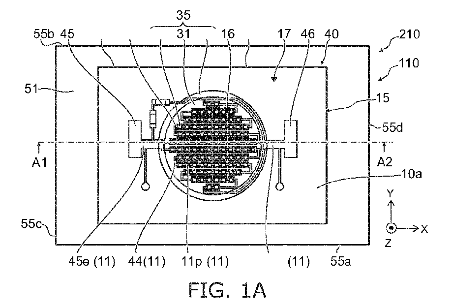
Description
- Embodiments described herein generally relate to a light-emitting device and a luminaire.
- For example, there is a light-emitting device in which a semiconductor light-emitting element that emits blue light and a phosphor that converts the wavelength of the light are combined to emit white light. The light-emitting device can be applied to, for example, a luminaire such as a floodlight. In such an application, a light amount per unit area is high. It is necessary to improve thermal radiation properties.
-
-
FIGS. 1A and 1B are schematic diagrams illustrating a light-emitting device and a luminaire according to a first embodiment; -
FIGS. 2A to 2C are schematic plan views illustrating the light-emitting device; -
FIG. 3 is a graph illustrating the light-emitting device; -
FIGS. 4A and 4B are schematic plan views illustrating the light-emitting device; -
FIG. 5 is a schematic sectional view illustrating the light-emitting device; -
FIG. 6 is a schematic sectional view illustrating the light-emitting device; -
FIG. 7 is a schematic sectional view illustrating another light-emitting device according to the first embodiment; -
FIG. 8 is a schematic sectional view illustrating a light-emitting device and a luminaire according to a fifth embodiment; -
FIGS. 9A and 9B are schematic diagrams illustrating the light-emitting device and the luminaire; -
FIGS. 10A to 10D are schematic sectional views illustrating other light-emitting devices and other luminaires according to the fifth embodiment; -
FIGS. 11A and 11B are schematic diagrams illustrating the light-emitting device and the luminaire; -
FIG. 12 is a graph illustrating characteristics of the light-emitting device and the luminaire; -
FIGS. 13A to 13F are schematic sectional views illustrating a light-emitting device and a luminaire according to a sixth embodiment; -
FIGS. 14A to 14G are schematic sectional views illustrating the light-emitting device; -
FIGS. 15A to 15G are schematic sectional views illustrating the light-emitting device; -
FIG. 16 is a schematic sectional view illustrating a light-emitting device and a luminaire according to a seventh embodiment; -
FIGS. 17A to 17C are schematic sectional views illustrating other light-emitting devices and other luminaires according to the seventh embodiment; -
FIGS. 18A to 18C are schematic sectional views illustrating other light-emitting devices and other luminaires according to the seventh embodiment; -
FIG. 19 is a diagram for explaining a light-emitting device according to an eighth embodiment; -
FIG. 20 is a diagram for explaining the cross section of the light-emitting device; -
FIG. 21 is a diagram for explaining a state in which members such as light-emitting elements and connectors are removed in the light-emitting device; -
FIG. 22 is a diagram for explaining a light-emitting device in the past; -
FIG. 23 is a diagram for explaining a light-emitting device according to a ninth embodiment; -
FIG. 24 is a diagram for explaining a light-emitting device according to a tenth embodiment; and -
FIG. 25 is a diagram for explaining a light-emitting device according to another embodiment. - In general, according to one embodiment, there is provided a light-emitting device including a light-emitting section, a thermal radiation member, and a heat conduction layer. The light-emitting section includes a mounting substrate section and a light-emitting element section. The mounting substrate section includes a substrate, a first metal layer, and a second metal layer. The substrate includes a first principal plane including a mounting region and a second principal plane on the opposite side of the first principal plane and is insulative. The first metal layer is provided on the first principal plane. The first metal layer includes a plurality of mounting patterns provided in the mounting region. The second metal layer is provided on the second principal plane and electrically insulated from the first metal layer. At least a part of the second metal layer overlaps the mounting region when projected on a first plane parallel to the first principal plane. The light-emitting element section includes a plurality of semiconductor light-emitting elements and a wavelength conversion layer. The plurality of semiconductor light-emitting elements are provided on the first principal plane. Each of the plurality of semiconductor light-emitting elements is electrically connected to any one mounting pattern among the plurality of mounting patterns and another one mounting pattern adjacent to the mounting pattern among the plurality of mounting patterns. The wavelength conversion layer covers at least parts of the plurality of semiconductor light-emitting elements, absorbs at least a part of first light emitted from the plurality of semiconductor light-emitting elements, and emits second light having a wavelength different from the wavelength of the first light. The luminous exitance of light emitted from the light-emitting element section is equal to or higher than 101 m/mm2 and equal to or lower than 1001 m/mm2. The thermal radiation member is opposed to the second principal plane. The thermal radiation member has an area equal to or larger than five times the area of the mounting region when projected on the first plane. The heat conduction layer is provided between the thermal radiation member and the second metal layer.
- According to another embodiment, there is provided a light-emitting device including a ceramic substrate, a first metal layer, a second metal layer, a third metal layer, a light-emitting section, a first connector, a second connector, and a thermal radiation plate. The ceramic substrate includes a first surface and a second surface. The second surface is located on the opposite side of the first surface. The ceramic substrate has a pair of first end sides and a pair of second end sides. The pair of second end sides are orthogonal to the first end sides. The pair of second end sides have length equal to or smaller than the length of the first end sides. The first metal layer and the second metal layer are formed on the first surface. The third metal layer is formed on the second surface. One end of the light-emitting section is electrically connected to one end side of the first metal layer. The other end of the light-emitting section is electrically connected to one end side of the second metal layer. The first connector is provided on the other end side of the first metal layer. The second connector is provided on the other end side of the second metal layer. The thermal radiation plate is made of metal. The thermal radiation plate is connected to the third metal layer to be opposed to the ceramic substrate via a solder layer. When an axis passing the center of the ceramic substrate and extending along the first end sides is represented as first axis and an axis passing the center of the ceramic substrate and extending along the second end sides is represented as second axis, the light-emitting section is arranged such that the center of the light-emitting section substantially coincides with the center of the ceramic substrate. The center of the light-emitting section, the first connector, and the second connector are arranged on the first axis. The first connector and the second connector are arranged to hold the light-emitting section therebetween.
- Embodiments are explained below with reference to the drawings.
- Note that the drawings are schematic or conceptual. Relations between the thicknesses and the widths of sections, ratios of sizes among the sections, and the like are not always the same as real ones. Even when the same sections are illustrated, the sections are illustrated in different dimensions and ratios depending on the drawings.
- In this specification and the drawings, components same as those already described with reference to the drawings are denoted by the same reference numerals and signs and detailed explanation of the components is omitted.
-
FIGS. 1A and 1B are schematic diagrams illustrating a light-emitting device and a luminaire according to a first embodiment. -
FIG. 1A is a plan view.FIG. 1B is a sectional view illustrating a part of an A1-A2 cross section ofFIG. 1A . - As illustrated in
FIGS. 1A and 1B , a light-emittingdevice 110 according to this embodiment includes a light-emittingsection 40, athermal radiation member 51, and aheat conduction layer 52. - The light-emitting
section 40 is provided on thethermal radiation member 51. Theheat conduction layer 52 is provided between thethermal radiation member 51 and the light-emittingsection 40. - That is, the
heat conduction layer 52 is provided on thethermal radiation member 51 and the light-emittingsection 40 is provided on theheat conduction layer 52. In this example, one light-emittingsection 40 is provided on thethermal radiation member 51. As explained below, a plurality of the light-emittingsections 40 may be provided on onethermal radiation member 51. - In this specification, a state in which a component is provided on the other component includes a state in which the component is directly provided on the other component and a state in which another component is inserted between the component and the other component.
- A direction extending from the
thermal radiation member 51 to the light-emittingsection 40 is referred to as superimposing direction. In this specification, a state in which components are superimposed includes a state in which the components are directly superimposed in contact with each other and a state in which the components are superimposed with another component inserted therebetween. - The superimposing direction is represented as Z-axis direction. One axis direction perpendicular to the Z-axis direction is represented as X-axis direction. A direction perpendicular to the Z-axis direction and perpendicular to the X-axis direction is represented as Y-axis direction.
- The
thermal radiation member 51 is, for example, tabular. The principal plane of thethermal radiation member 51 is, for example, substantially parallel to an X-Y plane. A plane shape of thethermal radiation member 51 is, for example, a rectangular shape. Thethermal radiation member 51 has, for example, first tofourth sides 55a to 55d. Thesecond side 55b is separated from thefirst side 55a. Thethird side 55c connects one end of thefirst side 55a and one end of thesecond side 55b. Thefourth side 55d is separated from thethird side 55c and connects the other end of thefirst side 55a and the other end of thesecond side 55b. A corner portion of the plane shape of thethermal radiation member 51 may be curved. The plane shape of thethermal radiation member 51 does not have to be the rectangular shape and is arbitrary. - A substrate made of metal or the like is used as the
thermal radiation member 51. Copper, aluminum, or the like is used as thethermal radiation member 51. - The light-emitting
section 40 emits light. At the same time, the light-emittingsection 40 emits heat. Theheat conduction layer 52 efficiently conducts the heat generated by the light-emittingsection 40 to thethermal radiation member 51. Solder or the like is used as theheat conduction layer 52. That is, theheat conduction layer 52 includes the solder. In this case, theheat conduction layer 52 joins the light-emittingsection 40 and thethermal radiation member 51. For example, an AuSn alloy or the like is used as theheat conduction layer 52. - Liquid or solid lubricant (grease) or the like may be used as the
heat conduction layer 52. In order to further improve heat conductivity than the heat conductivity of the lubricant (the grease), lubricant having conductivity obtained by mixing metal powder of alumina or the like in silicone (conductive grease) or the like may be used as theheat conduction layer 52. - The light-emitting
section 40 includes a mountingsubstrate section 15 and a light-emittingelement section 35. - The mounting
substrate section 15 includes asubstrate 10, afirst metal layer 11, and asecond metal layer 12. - The
substrate 10 includes a firstprincipal plane 10a and a secondprincipal plane 10b. The secondprincipal plane 10b is a surface on the opposite side of the firstprincipal plane 10a. Thethermal radiation member 51 is opposed to the secondprincipal plane 10b of thesubstrate 10. In other words, the secondprincipal plane 10b is a surface on thethermal radiation member 51 side. - In this specification, a state in which a component is opposed to the other component includes a state in which the components directly face each other and a state in which another component is inserted between the components.
- The first
principal plane 10a includes a mountingregion 16. For example, the mountingregion 16 is separated from anouter edge 10r of the firstprincipal plane 10a. In this example, the mountingregion 16 is provided in the center portion of the firstprincipal plane 10a. The firstprincipal plane 10a further includes aperipheral region 17. Theperipheral region 17 is provided around the mountingregion 16. An example of the mountingregion 16 is explained below. - The
substrate 10 is insulative. A ceramic substrate or the like is used as thesubstrate 10. For example, thesubstrate 10 includes alumina. For example, a ceramic substrate containing alumna as a main component is used as thesubstrate 10. - The
first metal layer 11 is provided on the firstprincipal plane 10a. Thefirst metal layer 11 includes a plurality of mountingpatterns 11p. The plurality of mountingpatterns 11p are provided in the mountingregion 16. At least any two or more of the plurality of mountingpatterns 11p are separated from one another. For example, at least any one of the plurality of mountingpatterns 11p is islet. Two of the plurality of mountingpatterns 11p are independent from each other. The plurality of mountingpatterns 11p includes, for example, a first mounting pattern 11pa and a second mounting pattern 11pb. - Each of the plurality of mounting
patters 11p includes, for example, a first mountingportion 11a and a second mountingportion 11b. In this example, the mountingpattern 11p further includes a third mountingportion 11c. The third mountingportion 11c is provided between the first mountingportion 11a and the second mountingportion 11b and connects the first mountingportion 11a and the second mountingportion 11b. An example of the mounting portions is explained below. - The
first metal layer 11 may further includes a connectingsection 44 configured to connect the plurality of mountingpatterns 11p one another. In this example, thefirst metal layer 11 further includes an electrode section forfirst connector 45e and an electrode section forsecond connector 46e. The electrode section forfirst connector 45e is electrically connected to one of the plurality of mountingpatterns 11p. The electrode section forsecond connector 46e is electrically connected another one of the plurality of mountingpatterns 11p. As explained below, a semiconductor light-emitting element is arranged on a part of one mountingpattern 11p. The electrode section forfirst connector 45e is electrically connected to one of the mountingpatterns 11p by the semiconductor light-emitting element. Further, a semiconductor light-emitting element is arranged on a part of another one mountingpattern 11p. The electrode section forsecond connector 46e is electrically connected to another one of the mountingpatterns 11p. - An example of the
first metal layer 11 is explained below. - In this example, the light-emitting
section 40 further includes afirst connector 45 and asecond connector 46 provided on the firstprincipal plane 10a. Thefirst connector 45 is electrically connected to the electrode section forfirst connector 45e. Thesecond connector 46 is electrically connected to the electrode section forsecond connector 46e. In this example, thefirst connector 45 is provided on the electrode section forfirst connector 45e. Thesecond connector 46 is provided on the electrode section forsecond connector 46e. The light-emittingelement section 35 is arranged between thefirst connector 45 and thesecond connector 46. Electric power is supplied to the light-emittingsection 40 via the connectors. - The
second metal layer 12 is provided on the secondprincipal plane 10b. Thesecond metal layer 12 is electrically insulated from thefirst metal layer 11. At least a part of thesecond metal layer 12 overlaps the mountingregion 16 when projected on an X-Y plane (a first plane parallel to the firstprincipal plane 10a). - As explained above, the
first metal layer 11 is provided on the upper surface (the firstprincipal plane 10a) of thesubstrate 10 and thesecond metal layer 12 is provided on the lower surface (the secondprincipal plane 10b) of thesubstrate 10. - The light-emitting
element section 35 is provided on the firstprincipal plane 10a of thesubstrate 10. The light-emittingelement section 35 includes a plurality of semiconductor light-emittingelements 20 and awavelength conversion layer 31. - The plurality of semiconductor light-emitting
elements 20 are provided on the firstprincipal plane 10a. Each of the plurality of semiconductor light-emittingelements 20 emits light. The semiconductor light-emittingelement 20 includes, for example, a nitride semiconductor. The semiconductor light-emittingelement 20 includes, for example, InyAlzGa1-x-yN (0≤x≤1, 0≤y≤1, x+y≤1). However, in this embodiment, a semiconductor light-emitting element is arbitrary. - The plurality of semiconductor light-emitting
elements 20 include, for example, a first semiconductor light-emittingelement 20a and a second semiconductor light-emittingelement 20b. Each of the plurality of semiconductor light-emittingelements 20 is electrically connected to any one mountingpattern 11p among the plurality of mountingpatterns 11p and another one mountingpattern 11p adjacent to the mountingpattern 11p among the plurality of mountingpatterns 11p. - For example, the first semiconductor light-emitting
element 20a is electrically connected to the first mounting pattern 11pa and the second mounting pattern 11pb among the plurality of mountingpatterns 11p. The second mounting pattern 11pb is equivalent to another mountingpattern 11p adjacent to the first mounting pattern 11pa. - For example, each of the plurality of semiconductor light-emitting
elements 20 includes afirst semiconductor layer 21 of a first conduction type, asecond semiconductor layer 22 of a second conduction type, and a light-emittinglayer 23. For example, the first conduction type is an n type and the second conduction type is a p type. The first conduction type may be the p type and the second conduction type may be the n type. - The
first semiconductor layer 21 includes a first portion (afirst semiconductor portion 21a) and a second portion (asecond semiconductor portion 21b). Thesecond semiconductor portion 21b is parallel to thefirst semiconductor portion 21a in the direction (e.g., the X-axis direction) crossing the superimposing direction (the Z-axis direction extending from thethermal radiation member 51 to the light-emitting section 40). - The
second semiconductor layer 22 is provided between thesecond semiconductor portion 21b and the mountingsubstrate portion 15. The light-emittinglayer 23 is provided between thesecond semiconductor portion 21b and thesecond semiconductor layer 22. - The semiconductor light-emitting
element 20 is, for example, an LED of a flip-chip type. - For example, the
first semiconductor portion 21a of thefirst semiconductor layer 21 is opposed to the first mountingportion 11a of the mountingpattern 11p. Thesecond semiconductor layer 22 is opposed to the second mountingportion 11b of the mountingpattern 11p. Thefirst semiconductor portion 21a of thefirst semiconductor layer 21 is electrically connected to the first mountingportion 11a. Thesecond semiconductor layer 22 is electrically connected to the second mountingportion 11b. Solder, a gold bump, or the like is used for the connection. The connection is performed by, for example, metal melting or solder joining. Alternatively, the connection is performed by, for example, an ultrasonic thermo-compression bonding method using a gold bump. - That is, for example, the light-emitting
element section 35 further includes a first joiningmetal member 21e and a second joiningmetal member 22e. The first joiningmetal member 21e is provided between thefirst semiconductor portion 21a and any one of the mountingpatterns 11p (e.g., the first mountingportion 11a). The second joiningmetal member 22e is provided between thesecond semiconductor layer 22 and another mountingpattern 11p (e.g., the second mounting pattern 11pb). At least one of the first joiningmetal member 21e and the second joiningmetal member 22e includes solder or a gold bump. Consequently, a sectional area (a sectional area cut along the X-Y plane) of each of the first joiningmetal member 21e and the second joiningmetal member 22e can be increased. Consequently, it is possible to efficiently transfer heat to the mountingsubstrate section 15 via the first joiningmetal member 21e and the second joiningmetal member 22e, and thereby improving heat radiation properties. - The
wavelength conversion layer 31 covers at least parts of the plurality of semiconductor light-emittingelements 20. Thewavelength conversion layer 31 absorbs at least a part of light (e.g., first light) emitted from the plurality of semiconductor light-emittingelements 20 and emits second light. The wavelength (e.g., peak wavelength) of the second light is different from the wavelength (e.g., peak wavelength) of the first light. Thewavelength conversion layer 31 includes a plurality of wavelength conversion particles such as phosphors and light transmissive resin in which the plurality of wavelength conversion particles are dispersed. The first light includes, for example, blue light. The second light includes light having wavelength larger than the wavelength of the first light. The second light includes, for example, at least one of yellow light and red light. - In this example, the light-emitting
element section 35 further includes a reflectinglayer 32. The reflectinglayer 32 surrounds thewavelength conversion layer 31 in the X-Y plane. The reflectinglayer 32 includes a plurality of particles such as metal oxides and light transmissive resin in which the particles are dispersed. The particles of the metal oxide or the like have light-reflectance. As the particles of the metal oxide or the like, for example, at least one of TiO2 and Al2O2 can be used. Since the reflectinglayer 32 is provided, light emitted from the semiconductor light-emittingelements 20 can be efficiently emitted along a direction (e.g., the upper direction) parallel to the superimposing direction. - The light-emitting
section 40 is, for example, an LED module of a chip-on-board (COB) type. - In this embodiment, the luminous exitance of light emitted from the light-emitting
element section 35 is equal to or higher than 101 m/mm2 (lumen/square millimeter) and equal to or lower than 1001 m/mm2. Desirably, the luminous exitance is equal to or higher than 201 m/mm2. That is, in this embodiment, a ratio of the light emitted from the light-emittingelement section 35 to a light emission area (luminous exitance) is extremely high. In this specification, the light emission area substantially corresponds to the area of the mountingregion 16. - The light-emitting
device 110 according to this embodiment is used for, for example, a floodlight. - As illustrated in
FIG. 1B , the light-emittingdevice 110 is arranged, for example, on aluminaire member 71. InFIG. 1A , theluminaire member 71 is omitted. Theluminaire member 71 is a part of a luminaire. A connecting member forluminaire 53 is provided between theluminaire member 71 and the light-emittingdevice 110. For example, solder or grease is used as the connecting member forluminaire 53. For example, the heat of the light-emittingdevice 110 is conducted to theluminaire member 71 by the connecting member forluminaire 53 and radiated. -
FIGS. 1A and 1B also illustrate the configuration of aluminaire 210 including the light-emittingdevice 110. Theluminaire 210 includes theluminaire member 71 and the light-emittingdevice 110. The light-emittingdevice 110 is provided on theluminaire member 71. Theluminaire 210 may further include the connecting member forluminaire 53. The connecting member forluminaire 53 is provided between theluminaire member 71 and the light-emittingdevice 110 and set in contact with thethermal radiation member 51 of the light-emittingdevice 110 and theluminaire member 71. The connecting member forluminaire 53 may be included in the light-emittingdevice 110. - In the light-emitting
device 110 according to this embodiment, thethermal radiation member 51 has an area equal to or larger than five times the area of the mountingregion 16 when projected on the X-Y plane (the first plane). - That is, in this embodiment, the area of the
thermal radiation member 51 is set extremely large with respect to the area of the mountingregion 16. Consequently, heat generated in the light-emittingelement section 35 provided on the mountingregion 16 is spread in an in-plane direction (an in-X-Y plane direction) by thethermal radiation member 51 having the large area. The heat spread in the in-plane direction is transmitted to, for example, theluminaire member 71, to which the light-emittingdevice 110 is attached, and efficiently radiated. - An example of the mounting
region 16, thefirst metal layer 11, and thesecond metal layer 12 is explained. -
FIGS. 2A to 2C are schematic plan views illustrating the light-emitting device according to the first embodiment -
FIG. 2A is a plan view illustrating a firstprincipal plane 10a of thesubstrate 10.FIG. 2B is a plan view illustrating a pattern of thefirst metal layer 11.FIG. 2C is a plan view illustrating a pattern of thesecond metal layer 12. - As illustrated in
FIG. 2A , the firstprincipal plane 10a includes the mountingregion 16 and theperipheral region 17. In this example, a pattern of the mountingregion 16 is substantially circular. The center of the mountingregion 16 is provided to substantially coincide with the center of thesubstrate 10. Theperipheral region 17 is a region around the mountingregion 16. - The area of the
peripheral region 17 is larger than the area of the mountingregion 16. The area of theperipheral region 17 is equal to or larger than four times the area of the mountingregion 16. The area of theperipheral region 17 is preferably equal to or smaller than nine times the area of the mountingregion 16. - For example, a distance (a shortest distance) between an end (the
outer edge 10r) of the firstprincipal plane 10a extending along one direction (e.g., the X-axis direction) parallel to the firstprincipal plane 10a and passing the center of the mountingregion 16 and the mountingregion 16 is equal to or larger than 1/2 of the width of the mountingregion 16 extending along the direction (the X-axis direction) passing the center. For example, a distance 17xa (a shortest distance) between theouter edge 10r extending along the X-axis direction and the mountingregion 16 is equal to or larger than 1/2 ofwidth 16x of the mountingregion 16. For example, a distance 17xb (a shortest distance) between theouter edge 10r extending along the X-axis direction and the mountingregion 16 is equal to or larger than 1/2 of thewidth 16x of the mountingregion 16. For example, a distance 17ya (a shortest distance) between theouter edge 10r extending along the Y-axis direction and the mountingregion 16 is equal to or larger than 1/2 ofwidth 16y of the mountingregion 16. For example, a distance 17yb (a shortest distance) between theouter edge 10r extending along the Y-axis direction and the mountingregion 16 is equal to or larger than 1/2 of thewidth 16y of the mountingregion 16. - Consequently, the area of the
peripheral region 17 is larger than the area of the mountingregion 16. Since the area of theperipheral region 17 is set larger than the area of the mountingregion 16 in which heat is generated, the generated heat efficiently spreads along the in-plane direction. Consequently, thermal radiation properties are improved. - As illustrated in
FIG. 2B , the plurality of mountingpatterns 11p, which are parts of thefirst metal layer 11, are provided in the mountingregion 16. In this example, the plurality of mountingpatterns 11p are provided in a circular region. In other words, a region where the plurality of mountingpatterns 11p are provided is the mountingregion 16. The mountingregion 16 is a region including the plurality of mountingpatterns 11p when projected on the X-Y plane. Regions among the plurality of mountingpatterns 11p are included in the mountingregion 16. The inner side of a line connecting, in a shortest distance, the outer edges of the mountingpatterns 11p arranged on the outer side among the plurality of mountingpatterns 11p is the mountingregion 16. - In order to improve the luminous exitance, the plurality of mounting
patterns 11p are arranged, for example, in a substantially circular region. In this case, practically, a substantially circular region including the plurality of mountingpatterns 11p may be used as the mountingregion 16. - The mounting
region 16 includes a region where the plurality of mountingpatterns 11p projected on the X-Y plane are provided. The mountingregion 16 does not include, when projected on the X-Y plane, a region where the connectingsection 44, the electrode section forfirst connector 45e, and the electrode section forsecond connector 46e are provided. The area is included in theperipheral region 17. - As explained above and illustrated in
FIG. 2B , parts of the plurality of mountingpatterns 11p are independent from one another. Independent two mountingpatterns 11p adjacent to each other are electrically connected by the semiconductor light-emittingelements 20 arranged on the mountingpatterns 11p. Parts of the plurality of semiconductor light-emittingelements 20 are, for example, connected in series. The plurality of semiconductor light-emittingelements 20 connected in series are, for example, arranged side by side along the X-axis direction. - Further, for example, two of the plurality of mounting
patterns 11p are connected by the connectingsection 44. Consequently, a group of the plurality of semiconductor light-emittingelements 20 connected in series is further connected. A group of the plurality of semiconductor light-emitting elements arranged side by side along the X axis and connected in series are arranged side by side along the Y-axis direction. A group of the plurality of semiconductor light-emitting elements arranged connected in series are connected in parallel to each other. - Further, the mounting
pattern 11p is electrically connected to the electrode section forfirst connector 45e or the electrode section forsecond connector 46e via awiring pattern 44c. An electric current is supplied to the mountingpatter 11p via thefirst connector 45 provided on the electrode section forfirst connector 45e and thesecond connector 46 provided on the electrode section forsecond connector 46e. The electric current is supplied to the semiconductor light-emittingelements 20 and light is generated. - As illustrated in
FIG. 2C , the area of thesecond metal layer 12 is designed large. The area of thesecond metal layer 12 is larger than the area of the mountingregion 16. The area of thesecond metal layer 12 projected on the X-Y plane (the first plane parallel to the superimposing direction) is equal to or larger than 95% of the area of the secondprincipal plane 10b. The efficiency of radiation of heat is improved by setting the area of thesecond metal layer 12 large. - A plane pattern of the heat
conductive layer 52 substantially extends along a pattern of thesecond metal layer 12. It is possible to expand the area of theheat conduction layer 52 by setting the area of thesecond metal layer 12 large. Consequently, it is possible to improve the efficiency of heat conduction via theheat conduction layer 52. - For example, an
outer edge 12r of thesecond metal layer 12 projected on the X-Y plane (the first plane) is located on the outer side of anouter edge 16r of the mountingregion 16. - The area of the
second metal layer 12 projected on the X-Y plane (the first plane) may be smaller than the area of the mountingregion 16. In this case, the area of thesecond metal layer 12 projected on the X-Y plane (the first plane) is still larger than 80% of the area of the mountingregion 16. If the area of thesecond metal layer 12 is smaller than 80% of the area of the mountingregion 16, the efficiency of thermal radiation falls. -
FIG. 3 is a graph illustrating the light-emitting device according to the first embodiment. -
FIG. 3 is an example of a change in light emission efficiency of the semiconductor light-emittingelements 20 that occurs when the area of thethermal radiation member 51 is changed. The abscissa ofFIG. 3 indicates a ratio Rs (Rs=S1/S2) of an area S1 of thethermal radiation member 51 to an area S2 of the mountingregion 16. The area S1 is an area of thethermal radiation member 51 projected on the X-Y plane (the first plane). The area S2 is an area of the mountingregion 16 projected on the X-Y plane. The ordinate ofFIG. 3 indicates light emission efficiency Eff (in an arbitrary unit). The light emission efficiency Eff of the semiconductor light-emittingelements 20 tends to fall when the temperature of the semiconductor light-emittingelements 20 rises. The light emission efficiency Eff corresponds to a temperature rise of the semiconductor light-emittingelements 20. That is, when the light emission efficiency Eff is high, the temperature of the semiconductor light-emittingelements 20 is maintained low. When the light emission efficiency Eff is low, the temperature of the semiconductor light-emittingelements 20 rises. In the example illustrated inFIG. 3 , the luminous exitance of light emitted from the light-emittingelement section 35 is equal to or higher than about 201 m/mm2. Thesecond metal layer 12 is provided on thesubstrate 10. Thesecond metal layer 12 is connected to thethermal radiation member 51 via theheat conduction layer 52. - As illustrated in
FIG. 3 , the light emission efficiency Eff is low when the ratio Rs of the area S1 of thethermal radiation member 51 to the area S2 of the mountingregion 16 is low. The light emission efficiency Eff is high when the ratio Rs is high. When the ratio Rs is lower than 5, the light emission efficiency Eff suddenly falls. This is because, when the area S1 of thethermal radiation member 51 is smaller than five times the area S2 of the mountingregion 16, heat generated in the light-emission element section 35 including the semiconductor light-emittingelements 20 and thewavelength conversion layer 31 is not sufficiently radiated in thethermal radiation member 51. Therefore, in this embodiment, the ratio Rs is set to be equal to or higher than 5. That is, the area S1 of thethermal radiation member 51 is set to be equal to or larger than five times the area S2 of the mountingregion 16. - As illustrated in
FIG. 3 , in a region where the ratio Rs is larger than 10, the light emission efficiency Eff tends to be saturated. When the ratio Rs is excessively high and the area S1 of thethermal radiation member 51 is excessively large, the size of the light-emitting device is excessively large. Therefore, when the light-emitting device is reduced in size, the area S1 of thethermal radiation member 51 is set to be equal to or larger than nine times the area S2 of the mountingregion 16. As illustrated inFIG. 3 , when the ratio Rs is equal to or larger than a fixed ratio, the light emission efficiency Eff does not substantially change and disadvantages such as an increase in size and an increase in cost occurs. Therefore, the ratio Rs is desirably equal to or smaller than twenty-two times. - The tendency illustrated in
FIG. 3 that the light emission efficiency Eff suddenly falls when the ratio Rs of the area S1 of thethermal radiation member 51 to the area S2 of the mountingregion 16 is low is not conspicuous when the luminous exitance of light emitted from the light-emittingelement section 35 is low. For example, when the luminous exitance is 21 m/mm2, a fall in the light emission efficiency Eff involved in a decrease of the ratio Rs is gentle. When the luminous exitance is equal to or higher than 101 m/mm2, when the ratio Rs decreases, the light emission efficiency Eff suddenly falls. Therefore, in this embodiment, when the luminous exitance is equal to or higher than 101 m/mm2, the ratio Rs is set to be equal to or higher than 5. - Originally, the size of the light-emitting device is preferably small. However, when the luminous exitance is high luminous exitance equal to or higher than 101 m/mm2, even if the size of the light-emitting device increases, the ratio Rs is set to be equal to or higher than 5 to obtain high light emission efficiency Eff. In this way, this embodiment has a configuration specially applied to a light-emitting device having high luminous exitance like a floodlight. According to this embodiment, even when the luminous exitance is high, it is possible to provide a light-emitting device with improved thermal radiation properties.
- As explained above, the area S1 of the
thermal radiation member 51 is set to be equal to or larger than five times the area S2 of the mountingregion 16. Similarly, the area of thesubstrate 10 is preferably set to be equal to or larger than five times the area S2 of the mountingregion 16. That is, in this embodiment, the area of theperipheral region 17 is set to be equal to or larger than four times the area of the mountingregion 16. Consequently, it is possible to obtain high light emission efficiency Eff. - In this embodiment, the
second metal layer 12 insulated from thefirst metal layer 11 is provided on the lower surface of thesubstrate 10. Thesecond metal layer 12 is not, for example, a route of an electric current supplied to the semiconductor light-emittingelements 20. Thesecond metal layer 12 is provided to obtain high thermal radiation properties. - For example, there is a configuration in which electrodes are provided in both the upper surface and the lower surface of the
substrate 10 and the electrodes provided on the lower surface and the electrodes provided on the upper surface are electrically connected by a through-hole that pierces through thesubstrate 10. For example, a semiconductor light-emitting element is connected to the electrodes provided on the upper surface. An electric current supplied to the semiconductor light-emitting element is supplied via the electrodes provided on the lower surface. In such a configuration, the electrodes provided on the lower surface form a route of the electric current supplied to the semiconductor light-emitting element. Therefore, (at least one of) the electrodes provided on the lower surface cannot be set in contact with thethermal radiation member 51 provided on the lower side of the electrodes. Therefore, thermal radiation via the electrodes provided on the lower surface is insufficient. - Such a configuration is considered to be applicable to a light-emitting device having low luminous exitance (e.g., a light-emitting device having luminous exitance lower than 101 m/mm2). However, when such a configuration is applied to a light-emitting device having high luminous exitance (e.g., a light-emitting device having luminous exitance equal to or higher than 101 m/mm2), thermal radiation becomes insufficient. As a result, sufficient thermal radiation properties are not obtained.
- In this way, the configuration in which the
second metal layer 12 insulated from thefirst metal layer 11 is provided on the lower surface of thesubstrate 10 is specially applied to the light-emitting device having high luminous exitance like a floodlight. Consequently, even when luminous exitance is high, it is possible to improve the thermal radiation properties. - In this embodiment, the heat conductivity of the
thermal radiation member 51 is equal to or higher than 300 W/(m·k) (watt/(meter·Kelvin)). The heat conductivity of theheat conduction layer 52 is equal to or higher than 5 W/(m·k) and desirably equal to or higher than 20 W/(m·K). Thickness t52 (seeFIG. 1B ) of theheat conductance layer 52 extending along the Z-axis direction (the superimposing direction extending from thethermal radiation member 51 to the light-emitting section 40) is equal to or smaller than 10 µm (micrometers). - Usually, aluminum is used as the
luminaire member 71. The heat conductivity of theluminaire member 71 is lower than the heat conductivity of thethermal radiation member 51. Since the heat conductivity of thethermal radiation member 51 is set to be equal to or higher than 300 W/(m·K), it is possible to sufficiently spread heat in the in-plane direction (in the in-X-Y plane direction) to theluminaire member 71. Consequently, the thermal radiation properties are improved. - Thermal resistance between a portion of highest temperature on an
upper surface 35u (seeFIG. 1B ) of the light-emittingelement section 35 and an edge portion 10ue (seeFIG. 1B ) of the firstprincipal plane 10a (the upper surface) of thesubstrate 10 is equal to or lower than 0.4°C/W (degree/watt). - Consequently, since a junction temperature of the semiconductor light-emitting
elements 20 falls, it is possible to improve the light emission efficiency. - Thermal resistance between an
edge portion 51r of thethermal radiation member 51 and the edge portion 10ue of the firstprincipal plane 10a (the upper surface) of thesubstrate 10 is equal to or lower than 0.1°C/W. - Consequently, since the junction temperature of the semiconductor light-emitting
elements 20 falls, it is possible to improve the light emission efficiency. Further, when solder is used as theheat conduction layer 52, it is possible to suppress a warp of thesubstrate 10 due to a difference in a coefficient of expansion. - In the light-emitting
device 110 according to this embodiment, a ratio of a voltage applied to the light-emittingelement section 35 to an electric current supplied to the light-emittingelement section 35 is equal to or higher than 100 V/A (volt/ampere) and equal to or lower than 1000 V/A. Since the ratio of the voltage to the electric current is set to be equal to or higher than 100 V/A, for example, it is possible to improve conversion efficiency of an inverter included in a lighting device. When the ratio of the voltage to the electric current exceeds 1000 V/A, the ratio is too high and an element is sometimes broken. Therefore, the ratio is not practical. - An example of the configuration of the mounting
patterns 11p and the semiconductor light-emittingelements 20 is explained. -
FIGS. 4A and 4B are schematic plan views illustrating the light-emitting device according to the first embodiment. -
FIG. 4A illustrates a pattern shape of the mountingpatterns 11p.FIG. 4B illustrates an arrangement of the semiconductor light-emittingelements 20. - As illustrated in
FIG. 4A , parts of the plurality of mountingpatterns 11p are arranged side by side along the X-axis direction. Further, a group of the plurality of mountingpatterns 11p arranged in the X-axis direction is arranged side by side along the Y-axis direction. - Each of the plurality of mounting
patterns 11p includes the first mountingportion 11a, the second mountingportion 11b, and the third mountingportion 11c. The third mountingportion 11c is provided between the first mountingportion 11a and the second mountingportion 11b and connects the first mountingportion 11a and the second mountingportion 11b. - In one mounting
pattern 11p, width w3 of the third mountingportion 11c extending along a traverse direction D2 perpendicular to a direction (an extending direction D1) extending from the first mountingportion 11a to the second mountingportion 11b is smaller than width w1 of the first mountingportion 11a extending along the traverse direction D2. The width w3 of the third mountingportion 11c extending along the traverse direction D2 is smaller than width w2 of the second mountingportion 11b extending along the traverse direction D2. - As illustrated in
FIG. 4B , the semiconductor light-emittingelements 20 are arranged on the mountingpatterns 11p. A part of the semiconductor light-emittingelements 20 is arranged, for example, on a part of the first mounting pattern 11pa. Another part of the semiconductor light-emittingelements 20 is arranged, for example, on a part of the second mounting pattern 11pb. For example, in one mountingpattern 11p (e.g., the first mounting pattern 11pa), the first mountingportion 11a is electrically connected to any one of the semiconductor light-emitting elements 20 (e.g., the first semiconductor light-emittingelement 20a). Thesecond mounting portion 11b is electrically connected to the second semiconductor light-emittingelement 20b. The second semiconductor light-emittingelement 20b is the semiconductor light-emittingelement 20 adjacent to the first semiconductor light-emittingelement 20a among the plurality of semiconductor light-emittingelements 20. - For example, the first mounting
portion 11a and the second mountingportion 11b of the mountingpattern 11p are covered by the semiconductor light-emittingelements 20. For example, the third mountingportion 11c of the mountingpattern 11p is not covered by the semiconductor light-emittingelements 20. - For example, as illustrated in
FIGS. 1B and4B , any one of the mountingpatterns 11p (e.g., the first mounting pattern 11pa) includes the first mountingportion 11a joined to any one of the semiconductor light-emitting elements 20 (e.g., the first semiconductor light-emittingelement 20a). Another mountingpattern 11p (the second mounting pattern 11pb adjacent to the first mounting pattern 11pa) includes the second mountingportion 11b joined to any one of the semiconductor light-emitting elements 20 (e.g., the first semiconductor light-emittingelement 20a). - As illustrated in
FIG. 4B , when projected on the X-Y plane (the first plane), any one of the semiconductor light-emitting elements 20 (e.g., the first semiconductor light-emittingelement 20a) includes aportion 26a further on the outer side than an outer edge 11ar of the first mountingportion 11a and aportion 26b further on the outer side than an outer edge 11br of the second mountingportion 11b. - For example, width w20 extending along the traverse direction D2 of each of the plurality of semiconductor light-emitting
elements 20 is larger than the width w1 of the first mountingportion 11a extending along the traverse direction D2 and larger than the width w2 of the second mountingportion 11b extending along the traverse direction D2. - For example, when projected on the X-Y plane (the first plane), each of the plurality of semiconductor light-emitting
elements 20 overlaps at least a part of the third mountingportion 11c. - Consequently, the first mounting
portion 11a and the second mountingportion 11b of the mountingpattern 11p are covered by the semiconductor light-emittingelement 20. - As explained above, for example, a ceramic substrate mainly containing alumina is used as the
substrate 10. The light-reflectance of the ceramic substrate is relatively high. For example, the reflectance of the surface (e.g., the firstprincipal plane 10a) of thesubstrate 10 is higher than the reflectance of the surface of each of the plurality of mountingpatterns 11p. For example, the reflectance of the surface of the mountingpattern 11p is relatively low. - Since the first mounting
portion 11a and the second mountingportion 11b of the mountingpattern 11p are covered by the semiconductor light-emittingelements 20, an area of the mountingpattern 11p having relatively low reflectance exposed to the surface can be reduced. Therefore, high reflectance can be obtained as a whole. In this configuration, even when solder is used as the first joiningmetal member 21e and the second joiningmetal member 22e, the solder less easily spreads to the side surfaces of the semiconductor light-emittingelements 20 when the semiconductor light-emittingelements 20 are mounted. In an LED of the flit-chip type, a semiconductor layer is sometimes exposed to the side surface because of a manufacturing method. By using this configuration, it is possible to suppress a short circuit from being caused by the solder. - The plurality of semiconductor light-emitting
elements 20 are separated from one another. Therefore, in the positions among the plurality of semiconductor light-emittingelements 20, the third mountingportions 11c of the mountingpatterns 11p are not covered by the semiconductor light-emittingelements 20. - As explained above, the width w3 of the third mounting
portion 11c extending along the traverse direction D2 is set smaller than the width w1 of the first mountingportion 11a and smaller than the width w2 of the second mountingportion 11b. Therefore, an exposed area of thesubstrate 10 having high reflectance can be increased. Consequently, high reflectance can be obtained as a whole. - For example, when the light-emitting
element section 35 is removed, average light-reflectance in the mountingregion 16 of the mountingsubstrate section 15 is equal to or higher than 70%. Since the arrangement explained above is adopted, such high light-reflectance can be obtained. -
FIG. 5 is a schematic sectional view illustrating the light-emitting device according to the first embodiment. -
FIG. 5 illustrates a part of the light-emittingsection 40. - As illustrated in
FIG. 5 , thefirst metal layer 11 includes acopper layer 13a (a Cu layer). Themetal layer 11 may further include a gold layer 13d (an Au layer). Thecopper layer 13a is provided between the gold layer 13d and thesubstrate 10. In this example, thefirst metal layer 11 further includes anickel layer 13b (an Ni layer) provided between thecopper layer 13a and the gold layer 13d and apalladium layer 13c (a Pd layer) provided between thenickel layer 13b and the gold layer 13d. In this way, in this example, thefirst metal layer 11 has a superimposed structure of Cu/Ni/Pd/Au. - On the other hand, the
second metal layer 12 includes acopper layer 14a. Thesecond metal layer 12 may further include agold layer 14d. Thecopper layer 14a is provided between thegold layer 14d and thesubstrate 10. In this example, thesecond metal layer 12 further includes anickel layer 14b provided between thecopper layer 14a and thegold layer 14d and apalladium layer 14c provided between thenickel layer 14b and thegold layer 14d. In this way, in this example, thesecond metal layer 12 has a superimposed structure of Cu/Ni/Pd/Au. - In the above explanation, boundaries among the copper layer, the nickel layer, the palladium layer, and the gold layer sometimes are not clear. Parts of these layers may have a mixed state of these kinds of metal (e.g., an alloy state).
- For the
second metal layer 12, for example, a material same as the material of thefirst metal layer 11 can be used. A superimposed structure same as the superimposed structure of thefirst metal layer 11 can be applied to thesecond metal layer 12. This makes it easy to form these metal layers. In this embodiment, the configuration of thesecond metal layer 12 may be different from the configuration of thefirst metal layer 11. - Thickness t11 of the
first metal layer 11 is, for example, equal to or larger than 30 µm and equal to or smaller than 100 µm and, for example, equal to or larger than 40 µm and equal to or smaller than 60 µm. Thickness t12 of thesecond metal layer 12 is, for example, equal to or larger than 30 µm and equal to or smaller than 100 µm and, for example, equal to or larger than 40 µm and equal to or smaller than 60 µm. - The
copper layer 13a of thefirst metal layer 11 and thecopper layer 14a of thesecond metal layer 12 can be formed by, for example, electrolytic plating. Each of the thickness of thecopper layer 13a and the thickness of thecopper layer 14a is, for example, equal to or larger than 30 µm and equal to or smaller than 100 µm and is, for example, about 50 µm. - The
nickel layer 13b, thepalladium layer 13c, and the gold layer 13d are formed by, for example, electroless plating. Thenickel layer 14b, thepalladium layer 14c, and thegold layer 14d are formed by, for example, electrolytic plating. - Each of the thickness of the
nickel layer 13b and the thickness of thenickel layer 14b is, for example, equal to or larger than 2 µm and equal to or smaller than 8 µm and is, for example, about 4.5 µm. Each of the thickness of thepalladium layer 13c and the thickness of thepalladium layer 14c is, for example, equal to or larger than 0.075 µm and equal to or smaller than 0.2 µm and is, for example, about 1 µm. Each of the thickness of the gold layer 13d and the thickness of thegold layer 14d is, for example, equal to or larger than 0.05 µm and equal to or smaller than 0.2 µm and is, for example, about 0.1 µm. - Since at least a part of the
first metal layer 11 and at least a part of thesecond metal layer 12 are formed by electroless plating, it is possible to substantially vertically form the side surfaces of thefirst metal layer 11 and the side surfaces of thesecond metal layer 12. - For example, a
side surface 11s of thefirst metal layer 11 cut along a plane (e.g., a second plane such as a Y-Z plane) perpendicular to the firstprincipal plane 10a can be formed substantially parallel to the superimposing direction (the Z-axis direction). An angle θ between theside surface 11s of thefirst metal layer 11 and the firstprincipal plane 10a is, for example, equal to or larger than 80 degrees and equal to or smaller than 95 degrees. The angle θ is more preferably, for example, equal to or larger than 85 degrees. - If the angle θ is small, the area of the lower surface of the mounting
pattern 11p is excessively large with respect to an area (e.g., the area of the upper surface) for mounting the mountingpattern 11p, which is a part of thefirst metal layer 11. Therefore, a ratio of a portion covered by the mountingpattern 11p in the upper surface (the firstprincipal plane 10a) of thesubstrate 10 is high. Therefore, it is difficult to increase the reflectance of the entire mountingregion 16. - Since the angle θ between the
side surface 11a of thefirst metal layer 11 and the firstprincipal plane 10a is set to be equal to or larger than 80 degrees and equal to or smaller than 95 degrees, it is possible to reduce the ratio of the portion covered by the mountingpattern 11p in the upper surface (the firstprincipal plane 10a) of thesubstrate 10. Consequently, it is possible to sufficiently increase the reflectance of the entire mountingregion 16. As a result, it is possible to improve the luminous exitance. - The curvature of a corner portion of the cross section of the
first metal layer 11 is relatively high. That is, the curvature radius of the corner portion is small. The cross section of thefirst metal layer 11 is close to a rectangle, i.e., theside surface 11s is close to a vertical. For example, thefirst metal layer 11 further includes anupper surface 11u parallel to the X-Y plane (the first plane). The curvature radius of a corner portion 11su connecting theupper surface 11u of thefirst metal layer 11 and theside surface 11s of thefirst metal layer 11 is equal to or smaller than 10 µm. Consequently, the area of the lower surface of the mountingpattern 11p can be reduced with respect to the area (e.g., the area of theupper surface 11u of the mountingpattern 11p) for mounting the mountingpattern 11p. As a result, it is possible to increase the reflectance of the entire mountingregion 16 and improve the luminous exitance. - In this example, a part of the
wavelength conversion layer 31 is arranged in aposition 11g (a space) between any one of the plurality of semiconductor light-emittingelements 20 and thesubstrate 10. Theposition 11g is a position between any one of the mountingpatterns 11p (e.g., the first mounting pattern 11pa) and another mountingpattern 11p (e.g., the second mounting pattern 11pb). Since a part of thewavelength conversion layer 31 is arranged in theposition 11g (the space) as well, it is possible to efficiently convert the first light emitted from the semiconductor light-emittingelement 20 into the second light in thewavelength conversion layer 31. In theposition 11g (the space), a wavelength conversion member including transparent resin or another phosphor material may be separately arranged. - In order to arrange a part of the
wavelength conversion layer 31 in theposition 11g (the space), a vacancy including theposition 11g may be increased. For example, a gap between the semiconductor light-emittingelement 20 and thesubstrate 10 is increased. For example, a distance tg between any one of the plurality of semiconductor light-emittingelements 20 and thesubstrate 10 extending along the Z-axis direction (the superimposing direction extending from thethermal radiation member 51 to the light-emitting section 40) is set relatively long. For example, the distance tg is equal to or larger than 1/10 of thickness t20 (height) of the plurality of semiconductor light-emittingelements 20 extending along the Z-axis direction. - For example, the height (the thickness t20 extending along the Z-axis direction) of the semiconductor light-emitting
layer 20 is, for example, equal to or larger than 50 µm and equal to or smaller than 500 µm and is, for example, 300 µm. The distance tg is, for example, equal to or larger than 40 µm and equal to or smaller than 110 µm and is, for example, 60 µm. It is possible to increase the distance tg by increasing the thickness t11 of thefirst metal layer 11. - In this embodiment, thickness t10 of the
substrate 10 is, for example, equal to or larger than 0.3 mm and equal to or smaller than 2 mm and is, for example, 0.635 mm. When the thickness t10 of thesubstrate 10 is smaller than 0.3 mm, for example, the mechanical strength of thesubstrate 10 decreases. When the thickness t10 of thesubstrate 10 exceeds 2 mm, for example, efficiency of conduction of heat generated by the semiconductor light-emitting elements 20 (the light-emitting element section 35) to thethermal radiation member 51 falls. - As illustrated in
FIG. 5 , thewavelength conversion layer 31 includes a plurality ofwavelength conversion particles 31a such as phosphors andlight transmissive resin 31b in which the plurality ofwavelength conversion particles 31a are dispersed. Thewavelength conversion particles 31a absorb at least a part of the first light emitted from the plurality of semiconductor light-emittingelements 20 and emits the second light having wavelength different from the wavelength of the first light. -
FIG. 6 is a schematic sectional view illustrating the light-emitting device according to the first embodiment. -
FIG. 6 is a sectional view equivalent to a cross section taken along line A1-A2 inFIG. 1A . - As illustrated in
FIG. 6 , the height of the connectors is preferably set to be equal to or smaller than the height of the light-emittingelement section 35. For example, a distance h45 (height) between the firstprincipal plane 10a of thesubstrate 10 and anupper surface 45u of thefirst connector 45 is equal to or smaller than 1.2 times a distance h35 (height) between the firstprincipal plane 10a of thesubstrate 10 and theupper surface 35u of the light-emittingelement section 35. For example, the distance h45 is preferably equal to or smaller than 1.1 times the distance h35. The distance h45 is more preferably equal to or smaller than the distance h35. - If the distance h45 is excessively large compared with the distance h35 and the
upper surface 45u of thefirst connector 45 is located excessively above theupper surface 35u of the light-emittingelement section 35, light (oblique light) emitted from the light-emittingelement section 35 is made incident on thefirst connector 45. The light is absorbed by thefirst connector 45 and lost. Further, deterioration of thefirst connector 45 is accelerated by the light. A reduction in the distance h45 and a reduction in the height of the upper surface of thefirst connector 45 make it easy to suppress the loss of the light and the deterioration of thefirst connector 45. - The same applies to the height of the
second connector 46. For example, a distance h46 (height) between the firstprincipal surface 10a of thesubstrate 10 and anupper surface 46u of thesecond connector 46 is equal to or smaller than 1.2 times the distance h35 (height) between the firstprincipal surface 10a of thesubstrate 10 and theupper surface 35u of the light-emittingelement section 35. For example, the distance h46 is preferably equal to or smaller than 1.1 times the distance h35. The distance h46 is more preferably equal to or smaller than the distance h35. This makes it easy to suppress a loss of light and deterioration of thesecond connector 46. - In this embodiment, the connectors are arranged apart from the mounting
region 16. For example, a distance L1 (a shortest distance parallel to the X-Y plane) between thefirst connector 45 and the mountingregion 16 is equal to or larger than 1/2 of thewidth 16x of the mountingregion 16. For example, a distance L2 (a shortest distance parallel to the X-Y plane) between thesecond connector 46 and the mountingregion 16 is equal to or larger than 1/2 of thewidth 16x of the mountingregion 16. Consequently, a degree of light (oblique light), which is emitted from the light-emittingelement section 35, made incident on thefirst connector 45 and thesecond connector 46 can be reduced. This makes it easy to suppress a loss of light and deterioration of the connectors. - In the light-emitting
device 110, laser printing is sometimes applied to thesubstrate 10. For example, a two-dimensional barcode is printed by the laser printing. In this case, the width of a region of the laser printing is preferably set to be equal to or smaller than 1/5 of the thickness t10 of thesubstrate 10. -
FIG. 7 is a schematic sectional view illustrating another light-emitting device according to the first embodiment. - As illustrated in
FIG. 7 , another light-emittingdevice 111 according to this embodiment includes thethermal radiation member 51, theheat conduction layer 52, and the plurality of light-emitting sections 40 (e.g., a first light-emittingsection 40a and a second light-emittingsection 40b). The configurations explained above can be applied to each of the plurality of light-emittingsections 40, thethermal radiation member 51, and theheat conduction layer 52.FIG. 7 illustrates the configuration of aluminaire 211 according to this embodiment as well. Theluminaire 211 includes theluminaire member 71 and the light-emittingdevice 111 provided on theluminaire member 71. - In the way, the plurality of light-emitting
section 40 may be provided for onethermal radiation member 51. Theheat conduction layer 52 is arranged between the plurality of light-emittingsections 40 and thethermal radiation member 51. Theheat conduction layer 52 can be divided for each of the plurality of light-emittingsections 40 or oneheat conduction layer 52 may be provided for the plurality of light-emittingsections 40. When theheat conduction layer 52 is divided, it can be considered that theheat conduction layer 52 has a plurality of patterns and a plurality of the heat conduction layers 52 are provided. - A second embodiment relates to the mounting
substrate section 15. The mountingsubstrate section 15 includes, for example, thesubstrate 10 and a conductive layer (e.g., the first metal layer 11) provided on thesubstrate 10. For example, as illustrated inFIG. 5 , the conductive layer (e.g., the first metal layer 11) includes a superimposed film including thenickel layer 13b, thepalladium layer 13c, and the gold layer 13d. For example, as explained above, thenickel layer 13b, thepalladium layer 13c, and the gold layer 13d are provided on thecopper layer 13a in this order. - A resist layer may be provided around the conductive layer provided on the
substrate 10. For example, a silicon material is used as the resist layer. A ceramic substrate having high reflectance is used as thesubstrate 10. - In this embodiment, a plated layer of Ni/Pd/Au is formed on a reflection surface of the
substrate 10. Consequently, for example, discoloration is suppressed. As a result, a fall in reflectance can be suppressed. Further, since the silicon material is used as the resist and the ceramic substrate having high reflectance is used, efficiency can be improved. - For example, when a plated layer of Ni/Ag is used as a reflection surface of a mounting substrate, discoloration occurs and a luminous flux tends to fall according to the discoloration. The discoloration is mainly affected by a sulfurous gas contained in the air. On the other hand, when a plated layer of Ni/Au is used, compared with the plated layer of Ni/Ag, total ray reflectance falls.
- In this embodiment, it is possible to improve resistance to sulfur corrosion and maintain high reflectance. Consequently, it is possible to suppress discoloration and obtain high efficiency.
- In this embodiment, a ceramic substrate of Al2O3 or the like can be used as the substrate. A metal substrate of Al or the like may be used as the substrate.
- For example, a plated layer of copper (the
copper layer 13a) is provided on a principal surface (either the upper surface or the lower surface) of the substrate. A superimposed film of Ni/Pd/Au is provided on the plated layer of copper. The superimposed film is formed by, for example, an electrolytic plating method or an electroless plating method. - In this embodiment, the total ray reflectance at a wavelength of 460 nm of the surface of the superimposed layer of Ni/Pd/Au (the surface of the gold layer 13d) is equal to or higher than 35% and equal to or lower than 50%. The total ray reflectance is, for example, a ratio of a total reflection luminous flux to a parallel incident luminous flux of a test piece. The total ray reflectance is ray reflectance including a diffusion component.
- In this embodiment, the total ray reflectance at a wavelength of 460 nm on the surface of the superimposed film of Ni/Pd/Au (the surface of the gold layer 13d) is equal to or higher than 60% and equal to or lower than 70%.
- In this embodiment, the thickness of the Ni layer is equal to or larger than 3 µm and equal to or smaller than 6 µm. The thickness of the Pd layer is equal to or larger than 0.05 µm and equal to or smaller than 0.1 µm. The thickness of the Au layer is equal to or larger than 0.05 µm and equal to or smaller than 3 µm.
- In this embodiment, the total ray reflectance at a wavelength of 460 nm of the substrate is equal to or higher than 85% and equal to or lower than 93%. The total ray reflectance at a wavelength of 560 nm of the substrate is equal to or higher than 85% and equal to or lower than 93%.
- The mounting substrate section according to this embodiment can be used for, for example, an LED module. The LED module can be used for, for example, a luminaire.
- A third embodiment relates to a COB module (e.g., the light-emitting element section 35). The COB module includes, for example, the semiconductor light-emitting
element 20 and thewavelength conversion layer 31. The semiconductor light-emittingelement 20 emits blue light. Thewavelength conversion layer 31 generates, for example, white visible light using the blue light as excitation light. The luminous exitance in the COB module is equal to or higher than 101 m/mm2. The power consumption of the COB module is equal to or larger than 50W. - In this embodiment, a connector for feeding electricity to the COB module is formed of metal. The connector has a unipolar structure. In one COB module, two or more connectors (e.g., the
first connector 45 and the second connector 46) are provided. - In the COB module, connectors containing resin is often used. On the other hand, in a high-power COB module used for a floodlight or the like, to satisfy a luminous intensity distribution characteristic, a light emission area (e.g., the area of the mounting region 16) is desirably small. When the light emission area is reduced and light emission density increases, deterioration due to light of the connectors arranged around the mounting
region 16 is intensified. Discoloration or the like sometimes occurs in the connectors. - According to an experiment, when the luminous exitance is equal to or higher than 101 m/mm2 and the module power is equal to or larger than 50 W, discoloration conspicuously occurs in the connectors containing resin. The discoloration occurs in the resin used for the connectors.
- In this embodiment, resin that causes discoloration is not used for the connectors. The connectors are formed of only metal. Consequently, it is possible to suppress discoloration of the connectors.
- In this embodiment, a plurality of connectors are provided, one of the connectors is used as a positive electrode, and another connector is used as a negative electrode.
- In this embodiment, for example, the
first connector 45 and thesecond connector 46 are arranged to hold the light-emittingelement section 35 therebetween. Consequently, the heat of the semiconductor light-emittingelement 20, which is a heat source on the firstprincipal plane 10a of thesubstrate 10, can be spread via thefirst metal layer 11 in advance. Therefore, the thermal radiation properties are further improved. - A fourth embodiment relates to the
wavelength conversion layer 31. As illustrated inFIG. 5 , thewavelength conversion layer 31 includes, for example, the plurality ofwavelength conversion particles 31a and thelight transmissive resin 31b (e.g., a sealing material). The plurality ofwavelength conversion particles 31a are dispersed in thelight transmissive resin 31b. In this embodiment, thelight transmissive resin 31b contains dimethyl silicone as a main component. The light-transmittance of thelight transmissive resin 31b is equal to or higher than 86%. The hardness (Shore A) of thelight transmissive resin 31b is equal to or higher than 15 and equal to or lower than 50. - The Shore A is, for example, a standard in measuring the hardness of general rubber. A penetrator (a pressing needle or an indenter) is pushed into the surface of an object to be measured and deformed. A deformation amount (press-in depth) of the penetrator is measured and converted into a numerical value. For the measurement of the Shore A, for example, a durometer (a spring-type rubber hardness meter) is used.
- In a COB module of a light-emitting device, in order to obtain high luminous exitance, semiconductor light-emitting elements are mounted on a substrate at high density. Therefore, thermal dissipation is poor. Further, an amount of light made incident on the
wavelength conversion layer 31 increases. Therefore, the temperature of thewavelength conversion layer 31 tends to rise. When silicone is used as light transmissive resin of thewavelength conversion layer 31, the heat conductivity of the silicone is about 0.1°C·W. Therefore, in a high-power COB module, compared with a small-power COB module, the temperature of thewavelength conversion layer 31 is extremely high. The hardness of the silicone rises according to the temperature. - Further, according to the temperature rise, heat stress is applied to the COB module. Therefore, a crack or peeling sometimes occurs between a wire (e.g., the first metal layer 11) used in the COB module and the
wavelength conversion layer 31. - In this embodiment, the hardness (the Shore A) of the
light transmissive resin 31b is set to be equal to or higher than 15 and equal to or lower than 50. Consequently, a crack and peeling can be suppressed. - This embodiment can include, for example, the light-emitting
element section 35 including the semiconductor light-emittingelements 20 configured to emit light having a wavelength equal to or larger than 400 nm and equal to or smaller than 480 nm and thewavelength conversion layer 31 configured to cover the semiconductor light-emittingelements 20. The luminous exitance in the light-emitting element section 35 (the COB module) is equal to or higher than 101 m/mm2 and the power consumption of the light-emittingelement section 35 is equal to or higher than 50 W. - When the thickness of the
light transmissive resin 31b of thewavelength conversion layer 31 is 2 mm, the total light transmittance for a wavelength of 400 nm of thelight transmissive resin 31b is equal to or higher than 85%. - According to this embodiment, it is possible to provide a light-emitting device having luminous exitance adaptable to a narrow angle of a floodlight or the like. Even when temperature rises during lighting, it is possible to reduce stress due to temperature stress and suppress a crack and peeling.
- An example of a result of an experiment concerning the light-emitting device according to this embodiment is explained.
- For example, the light-emitting
element section 35 is arranged on the mountingsubstrate section 15. The light-emittingsection 35 includes the plurality of semiconductor light-emittingelements 20. Each of the plurality of semiconductor light-emittingelements 20 is a square 1 mm on each side. The dominant wavelength of the semiconductor light-emittingelements 20 is 455 nm. In the arrangement of the plurality of semiconductor light-emittingelements 20, a pitch is 1.6 mm. The number of semiconductor light-emittingelements 20 is ninety-six. - In a first sample, dimethyl silicone having Shore A of 70 and elongation of 70% is used as the
light transmissive resin 31b of thewavelength conversion layer 31 of the light-emittingelement 35. In a second sample, dimethyl silicone having Shore A of 43 and elongation of 150% is used as thelight transmissive resin 31b. In a third sample, dimethyl silicone having Shore A of 32 and elongation of 200% is used as thelight transmissive resin 31b. - Concerning these samples, a lighting test is performed at an electric current of 440 mA, a voltage of 144 V, and junction temperature of 130°C. During the lighting test, the temperature on the upper surface of the
wavelength conversion layer 31 is equal to or higher than 120°C and equal to or lower than 150°C. - In the first sample, a crack occurs when about 100 hours elapse in the lighting test. In the second sample and the third sample, a crack does not occur when 2000 hours to 3000 hours elapse. Therefore, the Shore A is preferably equal to or lower than 50.
- On the other hand, when the shore A is lower than 15 and excessively low, workability is low. Therefore, in this embodiment, the Shore A is set to be equal to or higher than 15 and equal to or lower than 50. Consequently, a crack and peeling can be suppressed and workability is high.
- It is possible to suppress deterioration due to light by reducing absorption of light in a visible light region in the
light transmissive resin 31b. When the thickness of thelight transmissive resin 31b is 2 mm, the total light transmittance for a wavelength of 400 nm of thelight transmissive resin 31b is set to be equal to or higher than 85%, whereby high light extraction efficiency is obtained. The total light reflectance is more preferably equal to or higher than 90%. -
FIG. 8 is a schematic sectional view illustrating a light-emitting device and a luminaire according to a fifth embodiment. As illustrated inFIG. 8 , aluminaire 221 according to this embodiment includes a light-emittingdevice 121 and theluminaire member 71. Theluminaire member 71 includes, for example, abase section 72 and a reflectingsection 73. In this example, thebase section 72 is tabular. The reflectingsection 73 is provided along an edge of thebase section 72. The light-emittingdevice 121 is provided on thebase section 72. The reflectingsection 73 reflects light LL emitted from the light-emittingdevice 121. The light LL can be efficiently irradiated in a desired direction by the reflectingsection 73. Thebase section 72 efficiently radiates heat generated in the light-emittingdevice 121 while holding the light-emittingdevice 121. - In this example, the light-emitting
device 121 includes thethermal radiation member 51, theheat conduction layer 52, and the plurality of light-emitting sections 40 (e.g., the first light-emittingsection 40a and the second light-emittingsection 40b). - An interval among the plurality of light-emitting
sections 40 is preferably short. Consequently, the light LL having high intensity is emitted from a narrow region. If the light LL is emitted from a wide region, proper reflection is less easily obtained in the reflectingsection 73. It is difficult to perform highly efficient reflection in a desired direction. Therefore, it is preferable to bring a light emission characteristic closer to a point light source such that the light LL is emitted from the narrow region. Consequently, highly efficient reflection in the reflectingsection 73 is obtained. - In this embodiment, as in the embodiments explained above, by setting the ratio Rs to be equal to or higher than 5, even when the luminous exitance is as high as equal to or higher than 101 m/mm2 and equal to or lower than 1001 m/mm2, it is possible to provide a light-emitting device with improved thermal radiation properties.
- With a configuration explained below, for example, it is possible to practically reduce the interval among the plurality of light-emitting
sections 40. -
FIGS. 9A and 9B are schematic diagrams illustrating the light-emitting device and the luminaire according to the fifth embodiment. -
FIG. 9A is a plan view.FIG. 9B is a sectional view illustrating an A1-A2 line cross section ofFIG. 9A . - As illustrated in
FIGS. 9A and 9B , the light-emittingdevice 121 according to this embodiment includes thethermal radiation member 51, theheat conduction layer 52, and the plurality of light-emitting sections 40 (e.g., the first light-emittingsection 40a, the second light-emittingsection 40b, the third light-emittingsection 40c, and the fourth light-emittingsection 40d). The configurations explained in the first embodiment can be applied to each of the plurality of light-emittingsections 40, thethermal radiation member 51, and theheat conduction layer 52. In this example, theheat conduction layer 52 is divided for each of the plurality of light-emittingsections 40. The second light-emittingsection 40b is arranged side by side with the first light-emittingsection 40a in a surface parallel to the firstprincipal plane 10a. - For example, the
thermal radiation member 51 includes a substrate of copper and a nickel layer provided on the surface of the substrate. The nickel layer is formed by, for example, plating. For example, SnAg solder is used as theheat conduction layer 52. -
FIGS. 9A and 9B illustrate the configuration of theluminaire 221 according to this embodiment as well. Theluminaire 221 includes the luminaire member 71 (e.g., the base section 72) and the light-emittingdevice 121 provided on theluminaire member 71. - The first light-emitting
section 40a includes the plurality of semiconductor light-emitting elements 20 (the first semiconductor light-emittingelement 20a, the second semiconductor light-emittingelement 20b, etc.). The second light-emittingsection 40b includes the plurality of semiconductor light-emitting elements 20 (a third semiconductor light-emittingelement 20c, a fourth semiconductor light-emittingelement 20d, etc.). - For example, the first light-emitting
section 40a includes a first mountingsubstrate section 15a. The second light-emittingsection 40b includes a secondmounting substrate section 15b. The configuration of the mountingsubstrate section 15 explained in the first embodiment can be applied to each of the first mountingsubstrate section 15a and the second mountingsubstrate section 15b. - The
substrate 10 of one light-emitting section 40 (the first light-emittingsection 40a) among the plurality of light-emittingsections 40 includes a first side surface 10sa. The first side surface 10sa crosses the firstprincipal plane 10a. - The
substrate 10 of another light-emitting section 40 (the second light-emittingsection 40b) among the plurality of light-emittingsections 40 includes a second side surface 10sb. The second side surface 10sb crosses the firstprincipal plane 10a and is opposed to the first side surface 10sa. - The light-emitting
device 121 further includes a light reflectingresin layer 60. The light reflectingresin layer 60 is light-reflective and insulative. The light reflectingresin layer 60 covers at least a part of the first side surface 10sa and covers at least a part of the second side surface 10sb. - The light reflecting
resin layer 60 includes, for example, insulative resin and a plurality of particles dispersed in the insulative resin. For example, at least one of TiO2 and Al2O3 is used as the plurality of particles. For example, at least any one of silicon resin, epoxy resin, acrylic resin, and polyimide resin is used as the insulative resin. The reflectance of the light reflectingresin layer 60 is, for example, equal to or higher than 70%. Consequently, high insulation properties and high reflectance are obtained and light use efficiency is improved. - As explained above, it is sometimes preferable to reduce the interval among the light-emitting
sections 40. In order to reduce the interval among the plurality of light-emittingsections 40, for example, the area of thesubstrate 10 included in each of the plurality of light-emittingsections 40 is reduced. On the other hand, in thefirst metal layer 11 provided on the firstprincipal plane 10a and thesecond metal layer 12 provided on the secondprincipal plane 10b of thesubstrate 10, areas suitable therefor are necessary. - When the area of the
substrate 10 is reduced while the area of each of thefirst metal layer 11 and thesecond metal layer 12 is set proper, the distance between the end of thesubstrate 10 and the end of thefirst metal layer 11 is reduced and the distance between the end of thesubstrate 10 and the end of thesecond metal layer 12 is reduced. As a result, a creepage distance of insulation in these metal layers is reduced. - When the interval among the plurality of light-emitting
sections 40 is reduced in this way, a creepage distance of insulation in the mountingsubstrate section 15 is reduced. As a result, insulation properties tend to be deteriorated. - In this embodiment, the light
reflective resin layer 60 is provided among the mountingsubstrate sections 15 of the plurality of light-emittingsections 40 adjacent to one another. The light reflectingresin layer 60 covers at least a part of the first side surface 10sa. Consequently, even when the creepage distance of insulation in the first light-emittingsection 40a is reduced, satisfactory insulation properties can be maintained in the first mountingsubstrate section 15a. Similarly, the light reflectingresin layer 60 covers at least a part of the second side surface 10sb. Consequently, even when the creepage distance of insulation in the second light-emittingsection 40b is reduced, satisfactory insulation properties can be maintained in the second mountingsubstrate section 15b. - In this example, as illustrated in
FIG. 9B , the light reflectingresin layer 60 covers the first side surface 10sa and the second side surface 10sb and covers parts of the firstprincipal plane 10a of thesubstrate 10 of the one light-emitting section 40 (the first light-emittingsection 40a) and parts of the firstprincipal plane 10a of thesubstrate 10 of the other light-emitting section 40 (the second light-emittingsection 40b). For example, the light reflectingresin layer 60 covers parts of thefirst metal layer 11 of the first light-emittingsection 40a and parts of thefirst metal layer 11 of the second light-emittingsection 40b. Consequently, deterioration in the insulation properties is further suppressed. - For example, the light reflecting
resin layer 60 covers the side surfaces of thefirst metal layer 11 of the first light-emittingsection 40a and the side surfaces of thefirst metal layer 11 of the second light-emittingsection 40b. Consequently, insulation properties between the side surfaces of thefirst metal layer 11 of the first light-emittingsection 40a and the side surfaces of thefirst metal layer 11 of the second light-emittingsection 40b can be improved. - In this example, the light reflecting
resin layer 60 covers the side surfaces of thesecond metal layer 12 of the first light-emittingsection 40a and the side surfaces of thesecond metal layer 12 of the second light-emittingsection 40b. Consequently, insulation properties between the side surfaces of thesecond metal layer 12 of the first light-emittingsection 40a and the side surfaces of thesecond metal layer 12 of the second light-emittingsection 40b can be improved. - For example, when the interval among the plurality of light-emitting
sections 40 is reduced, insulation properties tend to be deteriorated among the metal layers included in each of the plurality of light-emittingsections 40. Since the light reflectingresin layer 60 covers the side surfaces of the metal layers included in each of the plurality of light-emittingsections 40, the insulation properties between the side surfaces can be improved. - As illustrated in
FIG. 9B , in this example, parts of the light reflectingresin layer 60 is arranged between thesubstrate 10 of the first mountingsubstrate section 15a of the first light-emittingsection 40a and thethermal radiation member 51. Further, parts of the light reflectingresin layer 60 is arranged between thesubstrate 10 of the second mountingsubstrate section 15b of the second light-emittingsection 40b and thethermal radiation member 51. The light reflectingresin layer 60 is filled in a space between the first mountingsubstrate section 15a and the second mountingsubstrate section 15b. Consequently, the insulation properties can be further improved. - Further, as illustrated in
FIG. 9A , in this example, the light reflectingresin layer 60 covers the outer edges of thesubstrates 10 included in the plurality of light-emittingsections 40. Consequently, the light use efficiency can be improved. - Since the light reflecting
resin layer 60 is provided, an interval between the first light-emittingsection 40a and the second light-emittingsection 40b can be reduced. For example, a distance g1 between the first side surface 10sa of thesubstrate 10 of the first light-emittingsection 40a and the second side surface 10sb of thesubstrate 10 of the second light-emittingsection 40b is equal to or larger than 0.5 millimeter (mm) and equal to or smaller than 5 millimeters (mm). The distance g1 is preferably equal to or smaller than 1 mm. - In this example, the
wavelength conversion layer 31 includes a firstwavelength conversion film 31p and a secondwavelength conversion film 31q. The firstwavelength conversion film 31p covers the side surfaces of the semiconductor light-emittingelements 20. The secondwavelength conversion film 31q covers the upper surfaces of the semiconductor light-emittingelements 20 and is provided on the firstwavelength conversion film 31p. The firstwavelength conversion film 31p emits, for example, red light. The secondwavelength conversion film 31q emits, for example, yellow light. -
FIGS. 10A to 10D are schematic sectional views illustrating other light-emitting devices and other luminaires according to the fifth embodiment. - In the figures, the
luminaire member 71 is omitted. The configuration explained concerning the first embodiment or the configuration explained concerning theluminaire 221 can be applied to theluminaire member 71 in these examples. - As illustrated in
FIGS. 10A to 10D , in light-emittingdevices 121a to 121d (andluminaires 221a to 221d) according to this embodiment, the light reflectingresin layer 60 covers the first side surface 10sa and the second side surface 10sb. Further, the light reflectingresin layer 60 covers parts of theprincipal plane 10a of thesubstrate 10 of the first light-emittingsection 40a and parts of the firstprincipal plane 10a of thesubstrate 10 of the second light-emittingsection 40b. - In the light-emitting
device 121a (and theluminaire 221a), the light reflectingresin layer 60 is separated from thefirst metal layer 11 and separated from thesecond metal layer 12. A part of the light reflectingresin layer 60 is arranged between thesubstrate 10 of the first mountingsubstrate section 15a and thethermal radiation member 51. Further, a part of the light reflectingresin layer 60 is arranged between thesubstrate 10 of the second mountingsubstrate section 15b and thethermal radiation member 51. - In the light-emitting
device 121b (and the luminaire 221b), the light reflectingresin layer 60 covers a part of thefirst metal layer 11 and is in contact with a part of thesecond metal layer 12. A part of the light reflectingresin layer 60 is arranged between thesubstrate 10 of the first mountingsubstrate section 15a and thethermal radiation member 51. A part of the light reflectingresin layer 60 is arranged between thesubstrate 10 of the second mountingsubstrate section 15b and thethermal radiation member 51. - In the light-emitting
device 121c (and theluminaire 221c), the light reflectingresin layer 60 is separated from thefirst metal layer 11 and separated from thesecond metal layer 12. The light reflectingresin layer 60 is not arranged between thesubstrate 10 of the first mountingsubstrate section 15a and thethermal radiation member 51 and between thesubstrate 10 of the second mountingsubstrate section 15b and thethermal radiation member 51. - In the light-emitting
device 121d (and theluminaire 221d), the light reflectingresin layer 60 covers a part of thefirst metal layer 11 and covers a part of thesecond metal layer 12. The light reflectingresin layer 60 is in contact with the reflectinglayer 32. A part of the light reflectingresin layer 60 is arranged between thesubstrate 10 of the first mountingsubstrate section 15a and thethermal radiation member 51. Further, a part of the light reflectingresin layer 60 is arranged between thesubstrate 10 of the second mountingsubstrate section 15b and thethermal radiation member 51. The light reflectingresin layer 60 is filled in the space between the first mountingsubstrate section 15a and the second mountingsubstrate section 15b. Consequently, higher insulation properties and higher reflectance can be obtained. -
FIGS. 11A and 11B are schematic diagrams illustrating the light-emitting device and the luminaire according to the fifth embodiment. - The figures illustrate the shape of the
thermal radiation member 51 according to this embodiment.FIG. 11A are plan view.FIG. 11B is an A1-A2 line sectional view ofFIG. 11A . - As illustrated in
FIG. 11A , thethermal radiation member 51 has first tofourth sides 55a to 55d. For example, thefirst side 55a extends along the X-axis direction. Thesecond side 55b is separated from thefirst side 55a and extends along the X-axis direction. Thethird side 55c connects one end of thefirst side 55a and one end of thesecond side 55b. Thefourth side 55d is separated from thethird side 55c and connects the other end of thefirst side 55a and the other end of thesecond side 55b. In this example, each of the length of thefirst side 55a and the length of thesecond side 55b is larger than each of the length of thethird side 55c and the length of thefourth side 55d. - As illustrated in
FIG. 11B , thethermal radiation member 51 may be warped. For example, thethermal radiation member 51 and the light-emittingsection 40 are joined at high temperature. Thethermal radiation member 51 is sometimes warped according to a difference in a coefficient of thermal expansion. - Attention is directed to the warp of the region where the mounting
substrate section 15 is provided in thethermal radiation member 51. As illustrated inFIG. 11A , the length of the region where the mountingsubstrate section 15 is provided is length L01 (mm) of a sum of length La (mm) of one mountingsubstrate section 15, length Lb (mm) of another mountingsubstrate section 15, and length Lc (mm) of a space between the mountingsubstrate sections 15. The length L01 is La+Lb+Lc. Warp C51 of thethermal radiation member 51 is a difference between positions in the Z-axis direction of the ends of the region of thethermal radiation member 51. For example, the warp C51 (mm) of thethermal radiation member 51 is a distance in the Z-axis direction between the end of the region on the lower surface of thethermal radiation member 51 and the center of the lower surface of thethermal radiation member 51. For example, the warp C51 of thethermal radiation member 51 may be a distance in the Z-axis direction between the end of the region on the upper surface of thethermal radiation member 51 and the center of the upper surface of thethermal radiation member 51. The warp C51 of thethermal radiation member 51 depends on the size of the region where the mountingsubstrate section 15 is provided. Relative warp RC1 is represented as C51/L01. - On the other hand, the
thermal radiation member 51 has thickness t51 (mm). The warp of thethermal radiation member 51 depends on the thickness t51 of thethermal radiation member 51. Relative thickness RT1 is represented as t51/L01. -
FIG. 12 is a graph illustrating a characteristic of the light-emitting device and the luminaire according to the fifth embodiment. -
FIG. 12 illustrates a simulation result of warp at 25°C obtained after thethermal radiation member 51 and the light-emittingsection 40 are joined at 217°C. Thethermal radiation member 51 and the light-emittingsection 40 are joined by the heat conduction layer 52 (e.g., solder). The abscissa ofFIG. 12 indicates the relative thickness RT1 of the thermal radiation member 51 (a heat spreader) and the ordinate indicates the relative warp RC1. - For example, the length L01 of the region where the mounting
substrate section 15 is provided in thethermal radiation member 51 is 50 mm. For example, when the relative thickness RT1 is 0.06, the thickness t51 of thethermal radiation member 51 is 3 mm. When the relative thickness RT1 is 0.12, the thickness t51 of thethermal radiation member 51 is 6 mm. When the relative warp RC1 is 0.004, the warp C51 is 0.2 mm. For example, when the length L01 of the region where the mountingsubstrate section 15 is provided in thethermal radiation member 51 is 50 mm, the warp C51 is preferably set to be equal to or smaller than 0.2 mm. Consequently, for example, highly efficient reflection in the reflectingsection 73 can be obtained. If the warp is excessively large, reflection in a proper direction of the light LL by the reflectingsection 73 is difficult. The thermal radiation properties could be worsened. Practically, the relative warp RC1 is preferably equal to or smaller than 0.004. Consequently, high efficiency by high reflection can be obtained. - From
FIG. 12 , the relative thickness RT1 is preferably 0.06. When the relative thickness RT1 increases, a change in the relative warp RC1 decreases. The relative thickness RT1 may be equal to or smaller than 0.12. When the relative thickness RT1 exceeds 0.12, a material use amount of thethermal radiation member 51 excessively increases. - Therefore, in this embodiment, the relative thickness RT1 is preferably equal to or larger than 0.06 and equal to or smaller than 0.12. That is, the thickness of the
thermal radiation member 51 is preferably equal to or larger than 0.6 times and equal to smaller than 0.12 times the length L01 of the region where the mountingsubstrate section 15 is provided in thethermal radiation member 51. - In general, in an LED module, when a plurality of COB modules are mounted on a heat spreader, to limit the mounting, an interval among the COB modules is set to be equal to or larger than a fixed interval. Therefore, the size of the LED module increases and the size of a reflecting mirror and an external size increase. In gaps formed among the COB modules, reflectance is low. Therefore, a reflection loss occurs.
- On the other hand, in a high-power COB module used for a floodlight or the like, it is preferable that the area of a light-emitting region is small and light emission density is high in order to satisfy a luminous intensity distribution characteristic. However, when the light emission density increases, the temperature in the center of the light-emitting region further rises. In a configuration in which a heat spreader is connected to each of a plurality of COB modules, fluctuation in temperature sometimes occurs in each of the plurality of COB modules.
- In this embodiment, a heat spreader and a plurality of COB modules are combined and, for example, white insulating resin (the light reflecting resin layer 60) is provided in regions among the plurality of COB modules. Consequently, for example, a creepage distance of insulation of a wiring substrate can be reduced. As a result, the size of the light-emitting device can be reduced.
- It is possible to reduce a light reflection loss by setting the reflectance of the white insulating resin to be equal to or higher than 70%.
- Since one heat spreader and the plurality of COB modules are combined, for example, a maximum temperature of the COB modules can be suppressed. Temperatures in the plurality of COB modules can be equalized. The light-emitting device can be reduced in size.
- In this embodiment, for example, solder is used as the
heat conduction layer 52. Consequently, for example, the thermal radiation properties can be improved. - In this embodiment, for example, it is possible to increase a heat spreader effect by setting the relative thickness RT1 to be equal to or larger than 0.015 and equal to or smaller than 0.03. Warp in the light-emitting device can be reduced.
-
FIGS. 13A to 13F are schematic sectional views illustrating a light-emitting device and a luminaire according to a sixth embodiment. -
FIG. 13A is a plan view of a light-emittingdevice 131 and aluminaire 231 according to this embodiment.FIG. 13B is a plan view of thethermal radiation member 51 included in the light-emittingdevice 131.FIG. 13C is a plan view of the mountingsubstrate section 15 included in the light-emittingdevice 131.FIGS. 13D, 13E, and 13F are respectively an A1-A2 line sectional view, an A3-A4 line sectional view, and an A5-A6 line sectional view ofFIG. 13A . - As illustrated in
FIG. 13A , theluminaire 231 according to this embodiment includes the light-emittingdevice 131 and theluminaire member 71. In this example, as in the example explained above, the light-emittingdevice 131 includes thethermal radiation member 51, theheat conduction layer 52, and the light-emittingsection 40. In this example, as in the example explained above, since the ratio Rs is set to be equal to or higher than 5, even when the luminous exitance is as high as equal to or higher than 101 m/mm2 and equal to or lower than 1001 m/mm2, it is possible to provide a light-emitting device with improved thermal radiation properties. - As illustrated in
FIGS. 13B, 13D, and 13F , a first surface (anupper surface 51u) of thethermal radiation member 51 opposed to the secondprincipal plane 10b hasirregularities 51p. - As illustrated in
FIG. 13B , for example, theirregularities 51p of the first surface (theupper surface 51u) include a plurality of first groves 51pa. The plurality of first grooves 51pa extend, for example, in the X-axis direction (e.g., a first direction parallel to the secondprincipal plane 10b). In this example, theirregularities 51p of the first surface (theupper surface 51u) further include a plurality of second grooves 51pb. The plurality of second grooves 51pb extend, for example, in the Y-axis direction (e.g., parallel to the secondprincipal plane 10b and crossing the first direction). In this example, the second direction is perpendicular to the first direction. In this embodiment, an angle between the first direction and the second direction is arbitrary. - As illustrated in
FIG. 13A , in this example, an outer edge 51pe formed when a region 51pr, where theirregularities 51p are provided, in the first surface (theupper surface 51u) is projected on the secondprincipal plane 10b is located on the outer side of an outer edge formed when thesubstrate 10 is projected on the secondprincipal plane 10b (e.g., theouter edge 10r of the firstprincipal plane 10a). - As illustrated in
FIGS. 13C, 13D, and 13F , in this example, a second surface (a lower surface 121) of thesecond metal layer 12 opposed to thethermal radiation member 51 hasirregularities 12p. - The
irregularities 12p of the second surface (the lower surface 121) include a plurality of third grooves 12pa. The plurality of third grooves 12pa extend, for example, in the X-axis direction (e.g., a third direction parallel to the secondprincipal plane 10b). In this embodiment, theirregularities 12p of the second surface (the lower surface 121) further includes a plurality of fourth grooves 12pb. The plurality of fourth grooves 12pb extend, for example, in the Y-axis direction (e.g., a fourth direction parallel to the secondprincipal plane 10b and crossing the third direction). In this example, the fourth direction is perpendicular to the third direction. In this embodiment, an angle between the third direction and the fourth direction is arbitrary. An angle between the third direction and the first direction, an angle between the third direction and the second direction, an angle between the fourth direction and the first direction, and an angle between the fourth direction and the second direction are arbitrary. - This embodiment is not limited to the above. The
irregularities 51p may include, for example, a plurality of independent convex portions and concave portions. Theirregularities 51p may include, for example, a plurality of independent concave portions and convex portions. Theirregularities 12p may include, for example, a plurality of independent convex portions and concave portions. Theirregularities 12p may include, for example, a plurality of independent concave portions and convex portions. - In this embodiment, at least one of the
irregularities 51p of thethermal radiation member 51 and theirregularities 12p of thesecond metal layer 12 may be provided. - The heat conduction layer 52 (e.g., solder) is filled in the concave portions of the
irregularities 51p and the concave portions of theirregularities 12p. Since the irregularities are provided, stress is further reduced. - For example, heat is generated in the light-emitting
section 40. For example, light emission efficiency (Im/W) in the semiconductor light-emittingelements 20 is reduced by the generated heat. When input power is increased, the temperature of the light-emitting device (e.g., the temperature of the semiconductor light-emitting elements 20) sometimes rises to be higher than a specification value of an environmental temperature of the light-emitting device. - For improvement of the thermal radiation properties, for example, there is a structure in which the rear surface of a COB and a thermal radiation plate (the thermal radiation member 51) are joined by solder (the heat conduction layer 52). In this structure, stress is applied to solder according to a difference in a coefficient of thermal expansion among the COB, the thermal radiation plate, and the solder. As a result, in some case, a crack occurs in the solder and reliability falls. There is a method of joining the COB and the thermal radiation plate via a material having small deformation resistance. However, satisfactory solder joining is less easily obtained. Further, in this method, a strain that occurs in a joined portion remains large. Therefore, when the COB or the thermal radiation plate warps, the strain concentrates and a crack tends to occur from a portion on which the strain concentrates.
- On the other hand, in this embodiment, at least one of the
irregularities 51p of thethermal radiation member 51 and theirregularities 12p of thesecond metal layer 12 are provided. Therefore, stress that occurs in the solder (the heat conduction layer 52) is reduced and a strain can be reduced. For example, stress in the X-Y plane is reduced by at least one of theirregularities 51p and theirregularities 12p. Consequently, the reliability can be improved. - Further, since the
irregularities 51p are provided, a contact area of thethermal radiation member 51 and the heat conduction layer 52 (e.g., the solder) expands. Since theirregularities 12p are provided, a contact area of thesecond metal layer 12 and the heat conduction layer 52 (e.g., the solder) expands. Consequently, the thermal radiation properties are improved. - In this way, since the irregularities are provided in at least one of the surface of the COB and the surface of the thermal radiation plate, stress can be reduced. Further, in the joining by the solder, a joining area can be increased and the thermal radiation properties are improved.
-
FIGS. 14A to 14G are schematic sectional views illustrating the light-emitting device according to the sixth embodiment. - The figures are sectional views of the
thermal radiation member 51 according to this embodiment taken along a plane including the Z-axis direction. - In examples illustrated in
FIGS. 14A and 14B , theirregularities 51p provided on theupper surface 51u of thethermal radiation member 51 include a concave portion 51pd. The concave portion 51pd includes a bottom surface portion (a thermal radiation member bottom surface portion 51qb) and a side surface portion (a thermal radiation member side surface portion 51qa). The side surface portion (the thermal radiation member side surface portion 51qa) crosses the secondprincipal plane 10b (i.e., the X-Y plane). In these examples, the cross section of thethermal radiation member 51 includes two thermal radiation member side surface portions 51qa. The cross section of a portion where the two thermal radiation member side surface portions 51qa cross (a thermal radiation member bottom surface portion 51qb) has a triangular shape. - In the example illustrated in
FIG. 14A , a convex portion 51pp of theupper surface 51u of thethermal radiation member 51 has a planar shape substantially parallel to theupper surface 51u of thethermal radiation member 51. In the example illustrated inFIG. 14B , the cross section of the convex portion 51pp of theupper surface 51u of thethermal radiation member 51 has a triangular shape. - In examples illustrated in
FIGS. 14C and 14D , as in the examples illustrated inFIGS. 14A and 14B , the concave portion 51pd of thethermal radiation member 51 includes the bottom surface portion (the thermal radiation member bottom surface portion 51qb) and the side surface portion (the thermal radiation member side surface portion 51qa). In the examples, the thermal radiation member bottom surface portion 51qb has a planar shape substantially parallel to the X-Y plane. - In the example illustrated in
FIG. 14C , the convex portion 51pp of theupper surface 51u of thethermal radiation member 51 has a planar shape substantially parallel to the X-Y plane. In the example illustrated inFIG. 14D , the cross section of the convex portion 51pp of theupper surface 51u of thethermal radiation member 51 has a triangular shape. - In examples illustrated in
FIGS. 14E, 14F, and 14G , the concave portion 51pd of thethermal radiation member 51 includes a corner portion (a thermal radiation member corner portion 51qc) in addition to the bottom surface portion (the thermal radiation member bottom surface portion 51qc) and the side surface portion (the thermal radiation member side surface portion 51qa). The thermal radiation member corner portion 51qc connects the thermal radiation member bottom portion 51qb and the thermal radiation member side surface portion 51qa and has a curved surface shape. - In the example illustrated in
FIG. 14E , the convex portion 51pp of theupper surface 51u of thethermal radiation member 51 has a planar shape substantially parallel to the X-Y plane. In the example illustrated inFIG. 14F , the convex portion 51pp of theupper surface 51u of thethermal radiation member 51 has a curved surface shape. In the example illustrated inFIG. 14(g) , the convex portion 55pp of theupper surface 51u of thethermal radiation member 51 has a planar shape substantially parallel to the X-Y plane. The thermal radiation member bottom surface section 51qb has a planar shape substantially parallel to the X-Y plane. - In this embodiment, it is preferable to provide a thermal radiation member corner portion 51qc having a curved surface shape. In this way, an edge portion (a corner portion) of the concave portion 51pd (e.g., a groove) is formed in a curved surface shape. Consequently, it is possible to suppress stress from concentrating on the edge portion of the concave portion 51pd of the
thermal radiation member 51. When the edge portion has a non-curved surface shape, a crack starts from the edge portion and a crack tends to occur. Since the edge portion is formed in a curved surface shape, it is possible to further suppress occurrence of a crack. -
FIGS. 15A to 15G are schematic sectional views illustrating the light-emitting device according to the sixth embodiment. - These figures are sectional views in which the
second metal layer 12 according to this embodiment is cut along a plane including the Z-axis direction. - In examples illustrated in
FIGS. 15A and 15B , theirregularities 12p provided on thelower surface 121 of thesecond metal layer 12 includes the concave portion 12pd. The concave portion 12pd includes the bottom surface portion (the second metal layer bottom surface portion 12qb) and the side surface portion (the second metal layer side portion 12qa). The side surface portion (the second metal layer side surface portion 12qa) crosses the secondprincipal plane 10b (i.e., the X-Y plane). In these examples, the cross section of thesecond metal layer 12 includes two second metal layer side surface portions 12qa. A portion where the two second metal layer side surface portions 12qa cross (the second metal layer bottom surface portion 12qb) has a triangular shape. - In the example illustrated in
FIG. 15A , the convex portion 12pp of thelower surface 121 of thesecond metal layer 12 has a planar shape substantially parallel to the X-Y plane. In the example illustrated inFIG. 15B , the cross section of the convex portion 12pp of thelower surface 121 of thesecond metal layer 12 has a triangular shape. - In examples illustrated in
FIGS. 15C and 15D , as in the examples explained above, the concave portion 12pd of thesecond metal layer 12 includes the bottom surface portion (the second metal layer bottom surface portion 12qb) and the side surface portion (the second metal layer side surface portion 12qa). In these examples, the second metal layer bottom surface portion 12qb has a planar shape substantially parallel to the X-Y plane. - In the example illustrated in
FIG. 15C , the convex portion 12pp of thelower surface 121 of thesecond metal layer 12 has a planar shape substantially parallel to the X-Y plane. In the example illustrated inFIG. 15D , the cross section of the convex portion 12pp of thelower surface 121 of thesecond metal layer 12 has a triangular shape. - In examples illustrated in
FIGS. 15E, 15F, and 15G , the concave portion 12pd of thesecond metal layer 12 includes a corner portion (a second metal layer corner portion 12qc) in addition to the bottom surface portion (the second metal layer bottom surface portion 12qb) and the side surface portion (the second metal layer side surface portion 12qa). The second metal layer corner portion 12qc connects the second metal layer bottom surface portion 12qb and the second metal layer side surface portion 12qa and has a curved surface shape. - In the example illustrated in
FIG. 15E , the convex portion 12pp of thelower surface 121 of thesecond metal layer 12 has a planar shape substantially parallel to the X-Y plane. In the example illustrated inFIG. 15F , the convex portion 12pp of thebottom surface 121 of thesecond metal layer 12 has a curved surface shape. In the example illustrated inFIG. 15G , the convex portion 12pp of thebottom surface 121 of thesecond metal layer 12 has a planar shape substantially parallel to the X-Y plane and the second metal layer bottom surface portion 12qb has a planar shape substantially parallel to the X-Y plane. - In this embodiment, it is preferable to provide the second metal layer corner portion 12qc having a curved surface shape. In this way, an edge portion (a corner portion) of the concave portion 12pd (e.g., a groove) is formed in a curved surface shape. Consequently, it is possible to suppress stress from concentrating on the edge portion of the concave portion 12pd of the
second metal layer 12. As a result, it is possible to further suppress occurrence of a crack. - In this embodiment, the shape of the concave portion (e.g., the groove) (a sectional shape of the concave portion cut along the plane including the Z-axis direction) can be, for example, a triangular shape, a trapezoidal shape, or a circular shape (an elliptical shape). When the shape is the triangular shape or the trapezoidal shape, it is preferable to form the corner portion in a curved surface shape.
- Depth d51 of the
irregularities 51p provided on the first surface (theupper surface 51u) of thethermal radiation member 51 is preferably equal to or smaller than 1/10 times the thickness t51 of the thermal radiation member 51 (seeFIG. 14G ). Since the depth d51 is set to be equal to or smaller than 1/10 times the thickness t51, for example, it is possible to suppress generation of a void in the solder (the heat conduction layer 52). Further, it is possible to suppress an amount of use of the solder and an increase in costs. When a higher effect is demanded, the depth d51 is desirably equal to or smaller than 1/20 times the thickness t51. The depth d51 is preferably equal to or larger than 1/1000 times the thickness t51 of thethermal radiation member 51. Consequently, it is possible to effectively suppress stress. Improvement of the thermal radiation properties through an increase in the contact area can be effectively obtained. - On the other hand, depth d12 of the
irregularities 12p provided on the second surface (the lower surface 121) of thesecond metal layer 12 is preferably equal to or smaller than 1/2 times the thickness t12 of the second metal layer 12 (seeFIG. 15G ). Since the depth d12 is set to be equal to or smaller than 1/2 times the thickness t12, for example, it is possible to suppress generation of a void in the solder (the heat conduction layer 52). Further, it is possible to suppress an amount of use of the solder and suppress an increase in costs. The depth d12 is preferably equal to or larger than 1/100 times the thickness t12 of thesecond metal layer 12. Consequently, it is possible to effectively suppress stress. Improvement of the thermal radiation properties through an increase in the contact area can be effectively obtained. - For example, a groove pitch is preferably equal to or larger than two times a groove depth.
- For example, a pitch of a plurality of the concave portions 51pd of the
thermal radiation member 51 is preferably equal to or larger than two times the depth of the concave portion 51pd. For example, the distance between bottom surface portions (the thermal radiation member bottom surface portions 51qb) of the plurality of concave portions 51pd adjacent to each other is preferably equal to or larger than two times the distance along the Z-axis direction between the convex portion 51pp of the concave portion 52pd and the bottom surface portion (the thermal radiation member bottom surface portion 51pd). Consequently, the shape of the concave portion 51pd (the shape of the groove) is easily stabilized. The pitch is more preferably equal to or larger than ten times the depth. Consequently, the shape of the concave portion (the groove) is easily equalized. - For example, a pitch of a plurality of the concave portions 12pd of the
second metal layer 12 is preferably equal to or larger than two times the depth of the concave portion 12pd. For example, the distance between bottom surface portions (the second metal layer bottom surface portions 12qb) of the plurality of concave portions 12pd adjacent to each other is preferably equal to or larger than two times the distance along the Z-axis direction between the convex portion 12pp of the concave portion 12pd and the bottom surface portion (the second metal layer bottom surface portion 12pb). Consequently, the shape of the concave portion 12pd (the shape of the groove) is easily stabilized. The pitch is more preferably equal to or larger than ten times the depth. Consequently, the shape of the concave portion (the groove) is easily equalized. - In this embodiment, the distance between the grooves is preferably equal to or larger than the depth of the groove.
- For example, the distance between the plurality of concave portions 51pd of the
thermal radiation member 51 is preferably equal to or larger than two times the depth of the concave portion 51pd. For example, the width (the distance in the direction perpendicular to the Z-axis direction) of the convex portions 51pp of the plurality of concave portions 51pd adjacent to each other is preferably equal to or larger than the distance along the Z-axis direction between the convex portion 51pp of the concave portion 52pd and the bottom surface portion (the thermal radiation member bottom surface portion 51pb). Consequently, a void in the concave portion 51pd (a void generated in the solder) is suppressed. When the distance between the grooves is excessively small, a void tends to remain. - For example, the distance between the plurality of concave portions 12pd of the
second metal layer 12 is preferably equal to or larger than the depth of the concave portion 12pd. For example, the width (the distance in the direction perpendicular to the Z-axis direction) of the convex portions 12pp of the plurality of concave portions 12pd adjacent to each other is preferably equal to or larger than the distance along the Z-axis direction between the convex portion 12pp of the concave portion 12pd and the bottom surface portion (the second metal layer bottom surface portion 12pb). Consequently, a void in the concave portion 12pd is suppressed. When the distance between the grooves is excessively small, a void tends to remain. - In this embodiment, for example, a ceramic substrate is used as the
substrate 10. Consequently, high heat conductivity and high insulation properties are obtained. Solder is used as theheat conduction layer 52. Consequently, high heat conductively is obtained. - When the ceramic substrate is used as the
substrate 10 and metal is used as theheat conduction layer 52, a large difference occurs in a coefficient of thermal expansion. In this embodiment, since the irregularities are provided, stress can be effectively reduced. - For example, a copper layer is used as the
second metal layer 12. Consequently, even when the solder is used as theheat conduction layer 52, satisfactory joining is obtained. A selection range for a material of the solder is widened and a condition range for a joining process is expanded. For example, aluminum may be used as thesecond metal layer 12. In this case, the material of the solder tends to be limited and the condition for the joining process tends to be limited. The heat conductivity of copper is higher than the heat conductivity of aluminum. Since the copper layer is used as thesecond metal layer 12, higher thermal radiation properties can be obtained. - As explained above, the outer edge 51pe formed when the region 51pr, where the
irregularities 51p are provided, in the first surface (theupper surface 51u) is projected on the secondprincipal plane 10b is preferably located on the outer side of an outer edge formed when the light-emitting region is projected on the secondprincipal plane 10b. Consequently, an effect of stress reduction can be obtained. The region 51pr is more desirably located on the outer side of an outer edge formed when thesubstrate 10 is projected on the secondprincipal plane 10b (e.g., theouter edge 10r of the firstprincipal plane 10a). Since the area where the irregularities are provided is widened, it is possible to more effectively suppress occurrence of a crack. -
FIG. 16 is a schematic sectional view illustrating a light-emitting device and a luminaire according to a seventh embodiment. - As illustrated in
FIG. 16 , aluminaire 241 according to this embodiment includes a light-emittingdevice 141 and theluminaire member 71. The light-emittingdevice 141 includes thethermal radiation member 51, theheat conduction layer 52, and the light-emittingsection 40. In this example, as in the examples explained above, by setting the ratio Rs to be equal to or higher than 5, even when the luminous exitance is as high as equal to or higher than 101 m/mm2 and equal to or lower than 1001 m/mm2, it is possible to provide a light-emitting device with improved thermal radiation properties. - In this example, as in the examples explained above, the light-emitting
element section 35 of the light-emittingsection 40 includes the plurality of semiconductor light-emittingelements 20 and thewavelength conversion layer 31. In this example, thereflection layer 32 is further provided. - Each of the plurality of semiconductor light-emitting elements 20 (e.g., the first semiconductor light-emitting
element 20a and the second semiconductor light-emittingelement 20b) includes a semiconductor light-emitting elementlower surface 201 opposed to the firstprincipal plane 10a and a semiconductor light-emitting elementupper surface 20u on the opposite side of the semiconductor light-emitting elementlower surface 201. The semiconductor light-emitting elementupper surface 20u is the upper surface of the semiconductor light-emittingelement 20. - On the other hand, the
wavelength conversion layer 31 includes a wavelength conversion layerlower surface 311 set in contact with the semiconductor light-emitting elementupper surface 20u and a wavelength conversion layerupper surface 31u on the opposite side of the wavelength conversion layerlower surface 311. The wavelength conversion layerupper surface 31u is the upper surface of thewavelength conversion layer 31. - In this embodiment, a distance t31 in the Z-axis direction (the direction perpendicular to the first
principal plane 10a) between the upper surface (the semiconductor light-emitting elementupper surface 20u) of any one of the plurality of semiconductor light-emittingelements 20 and the upper surface (the wavelength conversion layerupper surface 31u) of thewavelength conversion layer 31 is equal to or larger than 100 µm and equal to or smaller than 300 µm. - Consequently, high efficiency can be obtained, high heat conductivity is obtained in the
wavelength conversion layer 31, and a temperature rise can be suppressed. As a result, the life of thewavelength conversion layer 31 can be extended. - For example, as specification values of the light-emitting device according to this embodiment, for example, a correlated color temperature is 5000 K (Kelvin), a color rendering index is 70, and light emission efficiency at a package temperature of 90°C is, for example, 100 Im/W. That is, the luminous exitance is high. In the light-emitting device, a large number of LED chips are mounted. The
wavelength conversion layer 31 is provided around the LED chips. Light including a blue color is emitted from the LED chips. In thewavelength conversion layer 31, excitation is caused by the blue light, for example, yellow light is emitted, and white light is obtained. Thewavelength conversion layer 31 is designed such that the white light is appropriately obtained when the light is combined with the blue light. - The
wavelength conversion layer 31 includes resin (thelight transmissive resin 31b) and a plurality of phosphor particles (thewavelength conversion particles 31a) dispersed in the resin (seeFIG. 5 ). When the thickness of the wavelength conversion layer 31 (e.g., the distance t31) is large, the concentration of the phosphor particles is set low such that a proper light conversion characteristic can be obtained. Conversely, when the thickness of the wavelength conversion layer 31 (e.g., the distance t31) is thin, the concentration of the phosphor particles is set high. - The heat conductivity of the resin is lower than the heat conductivity of the phosphor particles. Therefore, when the concentration of the phosphor particles is low, the heat conductivity of the
wavelength conversion layer 31 is low. When the concentration of the phosphor particles is high, the heat conductivity of thewavelength conversion layer 31 is high. - When the distance t31 is excessively large and exceeds, for example, 500 µm, the concentration of the phosphor particles is set excessively low. Therefore, the heat conductivity in the
wavelength conversion layer 31 is low and the temperature of thewavelength conversion layer 31 excessively rises with the heat generated by the semiconductor light-emittingelements 20 and the heat generated by thewavelength conversion layer 31. Consequently, the life of thewavelength conversion layer 31 decreases. - In this embodiment, the distance t31 is set to be equal to or smaller than 300 µm. Consequently, the concentration of the phosphor particles changes to a proper value and the heat conductivity in the
wavelength conversion layer 31 can be reduced. As a result, the rise in temperature can be suppressed. For example, the life of thewavelength conversion layer 31 can be extended. - For example, since the distance t31 is set to be equal to or smaller than 300 µm, it is possible to form a state in which a part of the phosphor particles come into contact with one another. The number of phosphor particles that come into contact with the
substrate 10 and the LED chips (the semiconductor light-emitting elements 20) increases. Consequently, heat generated in the phosphor particles when a wavelength changes are easily transmitted to thesubstrate 10 and the LED chips. - On the other hand, when the thickness of the wavelength conversion layer 31 (e.g., the distance t31) is excessively small, the concentration of the phosphor particles in the
wavelength conversion layer 31 increases. That is, the distance among the plurality of phosphor particles decreases. Therefore, for example, probability that light emitted from one phosphor particle is absorbed (re-absorbed) by another phosphor particles located near the phosphor particles increases. That is, when the concentration of the phosphor particles is excessively high, the light emission efficiency falls. - In this embodiment, since the distance t31 is set to be equal to or larger than 100 µm, the concentration of the phosphor particles in the
wavelength conversion layer 31 becomes proper. Consequently, the re-absorption is suppressed and high light emission efficiency can be obtained. - In this embodiment, the LED chips (the semiconductor light-emitting elements 20) have, for example, a flip-chip structure. The
substrate 10 includes ceramic. In the case of the flip-chip structure, heat involved in light emission due to joining of carriers is mainly transmitted to thesubstrate 10 side. Consequently, in thesubstrate 10 of ceramic, heat can be effectively radiated and a temperature rise of the LED chip is suppressed. - A COB module is connected to the thermal discharge member 51 (a heat spreader) by the
heat conduction layer 52 such as conductive grease or solder. Consequently, it is possible to efficiently conduct and disperse the heat from the LED chips. As a result, an output can be increased. Further, for example, since a heat conduction route to thethermal discharge member 51 can be formed, the temperature of thewavelength conversion layer 31 can be maintained low. - Consequently, for example, in a COB module having high light emission efficiency equal to or higher than 251 m/W, the temperature of the
wavelength conversion layer 31 can be maintained low. Consequently, the life of thewavelength conversion layer 31 can be extended. - For example, as the semiconductor light-emitting
element 20, an LED chip , the length in the X-axis direction of which is 1 mm, the length in the Y-axis direction of which is 1 mm, and thickness (the length in the Z-axis direction) of which is 0.4 mm, is used. The plurality of semiconductor light-emittingelements 20 are arranged on thefirst metal layer 11 of the mountingsubstrate section 15. The reflectinglayer 32 is formed around the plurality of semiconductor light-emittingelements 20. The width (the inner diameter) of the reflectinglayer 32 is about 19 mm. In a region surrounded by the reflectinglayer 32, thewavelength conversion layer 31 is formed to cover the semiconductor light-emittingelements 20. For example, dimethyl silicone is used as resin of thewavelength conversion layer 31. A plurality of phosphor particles are dispersed in the resin. The concentration of the phosphor particles is about 17 weight percent. The height of the wavelength conversion layer 31 (the distance along the Z-axis direction between the firstprincipal plane 10a of thesubstrate 10 and the upper surface (the wavelength conversion layerupper surface 31u) of the wavelength conversion layer 31) is about 650 µm. The correlated color temperature of combined light of blue light emitted from the LED chips and light emitted from thewavelength conversion layer 31 is about 5000 K. That is, thewavelength conversion layer 31 is adjusted such that white light is obtained. The distance t31 is set to 150 µm. Such a light-emitting device is adopted as a fourth sample. - On the other hand, a light-emitting device in which the concentration of phosphor particles is set to about 8 weight percent is adopted as a fifth sample. In the fifth sample, the distance t31 is set to 500 µm. In the fifth sample, as in the fourth sample, the correlated color temperature of combined light of blue light emitted from the LED chips and light emitted from the
wavelength conversion layer 31 is about 5000 K. Conditions other than the concentration of the phosphor particles and the distance t31 are the same as the conditions in the forth sample. - In the fourth sample and the fifth sample, the light-emitting
section 40 is joined to thethermal radiation member 51 via theheat conduction layer 52 of solder. - The fourth sample and the fifth sample are lit and the temperature of the
wavelength conversion layer 31 is measured. In the fifth sample, the temperature of the surface (the wavelength conversion layerupper surface 31u) of thewavelength conversion layer 31 is 130°C. On the other hand, in the fourth sample, the temperature of the surface (the wavelength conversion layerupper surface 31u) of thewavelength conversion layer 31 is 110°C. Since the distance t31 is properly set in this way, a temperature rise of thewavelength conversion layer 31 can be suppressed. -
FIGS. 17A to 17C are schematic sectional views illustrating other light-emitting devices and other luminaires according to the seventh embodiment. - As illustrated in
FIG. 17A , in another light-emitting device 142 (and another luminaire 242) according to this embodiment, thewavelength conversion layer 31 is not provided between the semiconductor light-emittingelements 20 and thesubstrate 10. On the other hand, in the light-emitting device 141 (and the luminaire 241), thewavelength conversion layer 31 is provided between the semiconductor light-emittingelements 20 and thesubstrate 10 as well. Since thewavelength conversion layer 31 is filled in a space between the semiconductor light-emittingelements 20 and thesubstrate 10, for example, heat conductivity can be improved. - As illustrated in
FIGS. 17B and 17C , in another light-emitting device 143 (and another luminaire 243) according to this embodiment, the upper surface (the wavelength conversion layerupper surface 31u) of thewavelength conversion layer 31 is concaves in regions among the plurality of semiconductor light-emittingelements 20. The shape of the concaves is formed, for example, when thewavelength conversion layer 31 flows into a space between the semiconductor light-emittingelements 20 and the mountingsubstrate section 15. When parts of the upper surface of thewavelength conversion layer 31 are the concaves in this way, the distance to the flat surface of thewavelength conversion layer 31 is the distance t31. -
FIGS. 18A to 18C are schematic sectional views illustrating other light-emitting devices and other luminaires according to the seventh embodiment. - As illustrated in
FIG. 18A , in another light-emitting device 144 (and another luminaire 244) according to this embodiment,irregularities 31r are provided on the surface (in this example, the wavelength conversion layerupper surface 31u) of thewavelength conversion layer 31. The depth of theirregularities 31r is, for example, equal to or larger than 0.5 times and equal to or smaller than 5 times the wavelength of light emitted from thewavelength conversion layer 31. Light extraction efficiency from thewavelength conversion layer 31 can be improved by theirregularities 31r. - As illustrated in
FIG. 18B , in another light-emitting device 145 (and another luminaire 245) according to this embodiment, the surface of thewavelength conversion layer 31 is a semispherical shape that covers the semiconductor light-emittingelements 20. Theirregularities 31r are provided on the surface of thewavelength conversion layer 31. Light extraction efficiency from thewavelength conversion layer 31 can be improved by theirregularities 31r. - As illustrated in
FIG. 18C , in another light-emitting device 146 (and another luminaire 246) according to this embodiment, the surface (the upper surface) of thewavelength conversion layer 31 is concaves in parts among the plurality of semiconductor light-emittingelements 20. Theirregularities 31r are formed by the portions of the concaves. Light extraction efficiency from thewavelength conversion layer 31 can be improved by theirregularities 31r. - The light-emitting devices according to the embodiments explained above can be used as, for example, a luminaire such as a floodlight.
- A light-emitting device is a light source in which light-emitting elements are used. The light-emitting device is used for, for example, lighting and display. Since the light-emitting elements are point light sources, it is known that the light-emitting device has high heat generation density compared with a liner light source of a fluorescent lamp or the like. In recent years, there is a demand for a light-emitting device that emits high-intensity light in a narrow light emission area. Therefore, it is necessary to secure a structure for efficiently allowing heat generated in the light-emitting elements to escape.
- As an example for securing the thermal radiation properties, a thermal radiation plate made of metal is sometimes provided on the surface of a substrate on the opposite side of a surface on which the light-emitting elements are mounted. For connection of the substrate and the thermal radiation plate, a metal layer is formed on the rear surface of the substrate and the metal layer and the thermal radiation plate are joined by solder. Consequently, a thermal radiation path capable of transmitting the heat from the light-emitting elements to the thermal radiation plate is formed.
- However, when the substrate is ceramic, because of a difference in a coefficient of thermal expansion from the thermal radiation plate made of metal, large stress is applied to the solder and a crack occurs. When the stress is continuously applied, the crack expands and reliability is deteriorated. In an eighth embodiment, a light-emitting device with high reliability is provided.
- The eighth embodiment is explained with reference to
FIGS. 19, 20, and 21. FIG. 19 is a diagram for explaining a light-emitting device according to the eighth embodiment.FIG. 20 is a diagram for explaining the cross section of the light-emitting device.FIG. 20 is a diagram for explaining the cross section of the light-emitting device.FIG. 21 is a diagram for explaining a state in which members such as light-emitting elements and connectors are removed in the light-emitting device according to the eighth embodiment. - A light-emitting
device 380 according to this embodiment is a light-emitting device used for lighting and display. The light-emittingdevice 380 includes, as a main component, aceramic substrate 301 formed of a ceramic material such as alumina or alumina nitride, the ceramic material and a composite ceramic material, or the like. Theceramic substrate 301 includes afirst surface 311, which is the front surface, and asecond surface 312, which is the rear surface. Theceramic substrate 301 includes a pair of first end sides 313 and 314 and second end sides 315 and 316 orthogonal to thefirst end side 313 and shorter than the first end sides 313 and 314. That is, theceramic substrate 301 in this embodiment is a thin plate, the shape of thefirst surface 311 and thesecond surface 312 of which is a rectangular shape and the thickness of which is equal to or smaller than 1 mm. - The
ceramic substrate 301 is configured as a DPC (Direct Plated Copper) substrate. That is, in theceramic substrate 301, at least afirst metal layer 302 and asecond metal layer 303 are formed on thefirst surface 311 and a third metal layer 304 is formed on thesecond surface 312. Thefirst metal layer 302, thesecond metal layer 303, and the third metal layer 304 can be formed of the same material. For example, thefirst metal layer 302, thesecond metal layer 303, and the third metal layer 304 are formed by superimposing a first plated layer made of copper and having thickness equal to or smaller than 0.1 mm on a titanium oxide layer formed by sputtering. A second plated layer formed of nickel/gold or nickel/palladium/gold may be superimposed on the first plated layer. A total volume of the metal layers formed on thefirst surface 311 is desirably smaller than a total volume of the metal layer formed on thesecond surface 312. By adopting such a relation, it is possible to widen a forming region of a solder layer 364 interposed between theceramic substrate 301 and athermal radiation plate 310 explained below. Therefore, it is possible to secure a wide thermal radiation route for transmitting heat from light-emittingelements 352, which form a heat generating section, to thethermal radiation plate 310. Therefore, it is possible to improve thermal radiation properties. - A wiring pattern on the
first surface 311 of theceramic substrate 301 is explained in detail with reference toFIG. 21 . A first axis passing a center Cc of theceramic substrate 301 and extending along the first end sides 313 and 314 is represented as X axis. A second axis passing the center Cc and extending along the second end sides 315 and 316 is represented as Y axis. Thefirst metal layer 302 is formed near thesecond end side 315 on theceramic substrate 301 to coincide with the X axis. An end of thefirst metal layer 302 does not reach thesecond end side 315. In thefirst metal layer 302, a metal layer forpower feed 321 extending along the Y axis and projecting in the direction of thefirst end side 313 is formed at an end on thesecond end side 315 side. In thefirst metal layer 302, a metal layer forinspection 322 projecting in the direction of thefirst end side 314 along the Y axis is formed between an end on a light-emittingsection 305 side and the metal layer forpower feed 321. Further, a metal layer for component mounting 323 projecting in the direction of thefirst end side 313 along the Y axis is formed between the end on the light-emittingsection 305 side and the metal layer forinspection 322. - On the other hand, the
second metal layer 303 is formed near thesecond end side 316 on theceramic substrate 301 to coincide with the X-axis. An end of thefirst metal layer 302 does not reach thesecond end side 315. In thesecond metal layer 303, a metal layer forpower feed 331 projecting in the direction of thefirst end side 313 along the Y axis is formed at an end on thesecond end side 316 side. In thesecond metal layer 303, a metal layer forinspection 332 projecting in the direction of thefirst end side 314 along the Y axis is formed between an end on the light-emittingsection 305 side and the metal layer forpower feed 331. - The light-emitting
section 305 is provided on thefirst surface 311 of theceramic substrate 301. The light-emittingsection 305 is columnar. The light-emittingsection 305 includes a light-emittingsurface 351 from which light is emitted. The light-emittingsection 305 is arranged such that a center Cl thereof substantially coincides with the center Cc of theceramic substrate 301. That is, in the light-emittingsection 305, distances from the corners of theceramic substrate 301 to the center Cc are substantially the same. Note that "substantially" in this embodiment means that, for example, distances are optimally the same but a difference in a degree of a measurement error, for example, a difference of about 3 mm is permitted. - The light-emitting
section 305 includes the light-emittingelement 352. The light-emittingelement 352 is a light-emitting element of the flip-chip type that generate, for example, blue light. Specifically, a transparent sapphire layer, an n-type semiconductor layer, a light-emitting layer, and a p-type semiconductor layer are superimposed from one side to the other side in order. Electrodes are respectively formed in the n-type semiconductor layer and the p-type semiconductor layer. Electric power is supplied to the n-type semiconductor layer and the p-type semiconductor layer via a pair of electrodes, whereby light is generated in a light-emitting layer located on the lower side of the element. The light is emitted from the sapphire layer. In the light-emittingelement 352, one electrode is electrically connected to one end side of thefirst metal layer 302 and the other electrode is electrically connected to the other end side of the second metal layer 203 by asolder layer 361. - In this embodiment, the light-emitting
section 305 includes a plurality of the light-emittingelements 352. For example, ninety-six light-emittingelements 352 are provided. The plurality of light-emittingelements 352 are arranged to be divided into afirst section 353 and asecond section 354. Thefirst section 353 includes a half number of (e.g., forty-eight) light-emittingelements 352. In thefirst section 353, the plurality of light-emittingelements 352 are connected in series by a metal layer for element mounting 355 (an inter-element metal layer). In the plurality of light-emittingelements 352, one end of the metal layer for element mounting 355 is connected to thefirst metal layer 302 and the other end is connected to thesecond metal layer 303. On a connection side of thefirst section 353 to thesecond metal layer 303, a metal layer for component mounting 356 branching from the metal layer for element mounting 355 halfway extends in the direction of thefirst metal layer 302. For example, twocapacitors capacitors section 305. Similarly, thesecond section 354 includes a half number of (e.g., forty-eight) light-emittingelements 352. In thesecond section 354, the plurality of light-emittingelements 352 are connected in series by the metal layer for element mounting 355 (the inter-element metal layer). In the plurality of light-emittingelements 352, one end is connected to thefirst metal layer 302 and the other end is connected to thesecond metal layer 303. - The light-emitting
section 305 includes, for example, acylindrical wall section 357. Thewall section 357 is higher than the light-emittingelements 352 and is formed on thefirst surface 311 of theceramic substrate 301 to surround the light-emittingelements 352 in a cylinder of thewall section 357. A part of the light-emittingsection 305 is formed to be located on the metal layers (thefirst metal layer 302 and the second metal layer 303). Since thewall section 357 covers the light-emittingelements 352, thewall section 357 is desired to be formed of a material having high light reflectance. Thewall section 357 may include a bank inclining toward the front surface side. - In a space formed by the
wall section 357, theceramic substrate 301, and the like, sealingresin 358 formed of resin such as silicone is filled to cover the light-emittingelements 352. The sealingresin 358 includes a yellowish phosphor material. That is, a part of blue light generated by the light-emittingelements 352 is excited by the phosphor material included in the sealingresin 358 and changes to yellow light. Another part of the blue light generated by the light-emittingelements 352 is directly transmitted through the sealingresin 358. White light formed as a result of mixing of the blue light and the yellow light is emitted from the light-emittingsurface 351 of the light-emittingsection 305. A total luminous flux with respect to the area of the light-emittingsurface 351, a so-called luminous exitance is 101 m/mm2 to 1001 m/mm2. A total luminous flux with respect to total input power is 501 m/W to 1501 m/W. In this way, the light-emitting device emits high-intensity light in a small light-emission area. - On the other end side of the
first metal layer 302, i.e., on the metal layer forpower feed 321, afirst connector 308 is provided. Thefirst connector 308 is a member for supplying electric power to the light-emittingelements 352. Thefirst connector 308 is connected to a power feed line extended from a lighting device. Thefirst connector 308 includes a metal terminal. The first connector 308 (the metal terminal) is connected to thefirst metal layer 302 via asolder layer 362. On the other end side of thesecond metal layer 303, i.e., on the metal layer forpower feed 331, asecond connector 309 is provided. Like thefirst connector 308, thesecond connector 309 includes a metal terminal. The second connector 309 (the metal terminal) is connected to thesecond metal layer 303 via asolder layer 363. Thefirst connector 308 and thesecond connector 309 are arranged in positions symmetrical with respect to the Y axis. That is, a distance L31 between the light-emittingsection 305 and thefirst connector 308 and a distance L32 between the light-emittingsection 302 and thefirst connector 308 are substantially the same. Thefirst connector 308 and thesecond connector 309 are, for example, members that are likely to be heated when heat is transmitted thereto from the light-emittingelements 352, which are heat generation sources, via thefirst metal layer 302 and thesecond metal layer 303. Therefore, in order to suppress the heat from inclining to the center Cc of theceramic substrate 301, the distances L31 and L32 are desirably equal to or larger than 2 mm. On the other hand, in order to prevent the member, which could be heated, from approaching near a start point of a crack to expand the crack, the distance (a shortest distance L33) between an end of theceramic substrate 301 and the connectors (thefirst connector 308 and the second connector 309) is desirably equal to or larger than 5 mm. The metal terminals may be covered by an insulating case of resin or the like. - The
thermal radiation plate 310 is arranged on thesecond surface 312 of theceramic substrate 301. Thethermal radiation plate 310 functions as, for example, a heat spreader. Thethermal radiation plate 310 is, for example, a metal plate, the thickness of which is equal to or smaller than 5 mm. Thethermal radiation plate 310 is connected to the third metal layer 304 to face thesecond surface 312 of theceramic substrate 301 via, for example, the solder layer 364. - As explained above, in this embodiment, the light-emitting
section 305 is arranged such that the center Cl of the light-emittingsection 305 substantially coincides with the center Cc of theceramic substrate 1. Thefirst connector 308 and thesecond connector 309, which are unipolar connectors, are arranged at both the ends of the light-emittingsection 305 to be separated from the light-emittingsection 305. Therefore, it is possible to provide a light-emitting device with high reliability. That is, in the light-emitting device in which theceramic substrate 301 and thethermal radiation plate 310 are connected by the solder layer 364 and that emits high-intensity light in a narrow light emission area, large stress is applied to the solder layer 364 according to a difference in thermal expansion between lighting time and extinguishing time. Therefore, for example, a crack occurs in the solder layer 364. It is likely that the crack selectively expands and leads to deterioration in reliability. In this embodiment, it is possible to suppress the deterioration in reliability. - This is more specifically explained with reference to a light-emitting device in the past. As illustrated in
FIG. 22 , in a light-emittingdevice 480, a light-emittingsection 405 is arranged in a position deviated from the center on afirst surface 411 of aceramic substrate 401. In the light-emittingdevice 480, abipolar connector 408 is arranged. In the light-emittingdevice 480, it is particularly highly likely that deterioration in reliability occurs. Portions to be heated in the light-emittingdevice 480 are the light-emittingsection 405 including light-emitting elements 452 (not illustrated in the figure), which are heat generation sources, and theconnector 408 including an anode connector and a cathode connector to which the heat of the light-emittingsection 405 is transmitted via first andsecond metal layers ceramic substrate 401 as illustrated inFIG. 22 , a heat distribution becomes uneven. Therefore, a crack occurs, for example, in a solder layer 464 (not illustrated in the figure) near a corner of theceramic substrate 401. When projected on the X-Y plane, the crack gradually expands in the center direction of theceramic substrate 401 in the solder layer 464. The expansion of the crack is more conspicuous in a portion where temperature is higher. Therefore, the uneven heat distribution leads to local expansion of the crack. If the crack of the solder layer 464 expands to the rear side of the light-emittingsection 405 even partially, in some case, a thermal radiation route from the light-emitting elements 452 to athermal radiation plate 410 is cut and the light-emitting elements 452 are broken. - Therefore, in the light-emitting
device 380 according to the eighth embodiment, the light-emittingsection 305 is arranged in the center Cc of theceramic substrate 301. The unipolar connectors (thefirst connector 308 and the second connector 309) are arranged at both the ends of the light-emittingsection 305 to be separated from the light-emittingsection 305. Therefore, the heat generation sources are dispersed and the uneven heat distribution on theceramic substrate 301 is solved. Local occurrence of a crack can be suppressed. Expansion of a crack can be delayed. Further, the light-emittingsection 305 is arranged to be separated from the corner of theceramic substrate 301, which could be a start point of a crack. Therefore, it is possible to sufficiently delay time when the crack reaches the rear side of the light-emittingsection 305. Accordingly, it is possible to provide a light-emitting device with high reliability. Thecapacitors first connector 308. Since heat generation of thecapacitors - The
first connector 308 and thesecond connector 309 are provided to be symmetrical to each other with respect to the Y axis. Therefore, the heat distribution is equalized and the reliability is further improved. The plurality of light-emittingelements 352 are provided to be symmetrical to one another with respect to the X axis and the Y axis. Therefore, the heat distribution is equalized and the reliability is further improved. Further, thefirst connector 308 and thesecond connector 309 are connected to thefirst metal layer 302 and thesecond metal layer 303 such that the longitudinal direction of thefirst connector 308 and thesecond connector 309 extends along the Y axis. Therefore, the reliability is further improved. -
FIG. 23 is a diagram for explaining a light-emitting device according to a ninth embodiment. Sections in the ninth embodiment same as the sections in the eighth embodiment are denoted by the same reference numerals and signs and explanation of the sections is omitted. - In a light-emitting
device 381 according to this embodiment, the shape of thefirst surface 311 of theceramic substrate 301 is an elliptical shape. The center Cl of the light-emittingsection 305, thefirst connector 308, and thesecond connector 309 are arranged on the X axis passing the center Cc of theceramic substrate 301, extending along the end sides of thethermal radiation plate 310, and passing a portion where the width of theceramic substrate 301 is the largest. - In the ninth embodiment, as in the eighth embodiment, an uneven heat distribution is equalized. Therefore, it is possible to provide a light-emitting device with high reliability. Tenth Embodiment
-
FIG. 24 is a diagram for explaining a light-emitting device according to a tenth embodiment. - In a light-emitting
device 382 according to this embodiment, the shape of thefirst surface 311 of theceramic substrate 301 is a polygonal shape. Theceramic substrate 301 is formed in a polygonal shape by, for example, providingcutout sections 317 obliquely at the four corners of the rectangularceramic substrate 301. The center Cl of the light-emittingsection 305, thefirst connector 308, and thesecond connector 309 are arranged on the X axis passing the center Cc of theceramic substrate 301, extending along the end sides of thethermal radiation plate 310, and passing a portion where the width of theceramic substrate 301 is the largest. - In the tenth embodiment, as in the eighth embodiment, an uneven heat distribution is equalized. Therefore, it is possible to provide a light-emitting device with high reliability.
- The present invention is not limited to the embodiments explained above. Various modifications are possible.
- For example, the light-emitting
section 305 is not limited to the columnar shape and may be an elliptic columnar shape or a polygonal columnar shape. - The light-emitting
element 352 is not limited to the light-emitting element of the flip-chip type and may be a light-emitting element of a face-up type electrically connected using a boning wire. - As in the light-emitting
device 384 illustrated inFIG. 25 , thefirst connector 308 and thesecond connector 309 may be arranged to be symmetrical to each other with respect to the center Cc of theceramic substrate 301. The same applies to patterns in parts of thefirst metal layer 302 and thesecond metal layer 303. - According to another embodiment, there is provided a light-emitting device including a ceramic substrate, a first metal layer, a second metal layer, a third metal layer, a light-emitting section, a first connector, a second connector, and a thermal radiation plate. The ceramic substrate includes a first surface and a second surface. The ceramic substrate is circular or polygonal. The first metal layer and the second metal layer are formed on the first surface. The third metal layer is formed on the second surface. The light-emitting section includes a light-emitting element, one end of which is electrically connected to one end side of the first metal layer and the other end of which is electrically connected to one end side of the second metal layer. The first connector is provided on the other end side of the first metal layer. The second connector is provided on the other end side of the second metal layer. The thermal radiation plate is made of metal. The thermal radiation plate is connected to the third metal layer to be opposed to the ceramic substrate via a solder layer. When an axis passing the center of the ceramic substrate and passing a portion having largest width of the ceramic substrate is represented as first axis and an axis passing the center of the ceramic substrate and orthogonal to the first axis is represented as second axis, the light-emitting section is arranged such that the center of the light-emitting section substantially coincides with the center of the ceramic substrate. The center of the light-emitting section, the first connector, and the second connector are arranged on the first axis. The first connector and the second connector are arranged to hold the light-emitting section therebetween.
- According to the embodiments, a light-emitting device and a luminaire with improved thermal radiation properties are provided.
- In this specification, "vertical" and "parallel" do not always mean "strictly vertical" and "strictly parallel" and allow, for example, fluctuation in a manufacturing process. "Substantially vertical" and "substantially parallel" are sufficient.
- The embodiments are explained above with reference to the specific examples. However, the embodiments are not limited to the specific examples. For example, specific configurations of the components such as the light-emitting section, the mounting substrate section, the light-emitting element section, the substrate, the first metal layer, the second metal layer, the semiconductor light-emitting element, the wavelength conversion layer, the reflecting layer, the thermal radiation member, the heat conduction layer, the light reflecting resin layer, the ceramic substrate, the first metal layer, the second metal layer, the third metal layer, the first connector, the second connector, the thermal radiation plate, the wall section, the inter-element metal layer, and the sealing resin included in the light-emitting device and the luminaire member, the luminaire connecting member, the base section, and the reflecting section included in the luminaire are included in the scope of the invention as long as those skilled in the art can carry out the invention in the same manner and obtain the same effects by selecting the configurations as appropriate from the publicly-known range.
- Components obtained by combining any two or more components among the components in the specific examples in a technically possible range are also included in the scope of the invention as long as the components imply the gist of the invention.
- Besides, all light-emitting devices and luminaires that those skilled in the art can carry out by changing designs as appropriate on the basis of the light-emitting devices and the luminaires explained above as the embodiments also belong to the scope of the invention as long as the light-emitting devices and the luminaires imply the gist of the invention.
- Further, in the category of the idea of the invention, those skilled in the art can arrive at various alternations and modifications. It is understood that the alternations and the modifications also belong to the scope of the invention.
- While certain embodiments have been described, these embodiments have been presented by way of example only, and are not intended to limit the scope of the inventions. Indeed, the novel embodiments described herein may be embodied in a variety of other forms; furthermore, various omissions, substitutions and changes in the form of the embodiments described herein may be made without departing from the spirit of the inventions. The accompanying claims and their equivalents are intended to cover such forms or modifications as would fall within the scope and spirit of the inventions.
Claims (13)
- A light-emitting device (110, 111, 121, 121a, 121b, 121c, 121d, 131, 141) comprising:a light-emitting section (40, 40a, 40b, 40c, 40d) including:a mounting substrate section (15) including:an insulative substrate (10) including a first principal plane (10a) including a mounting region (16) and a second principal plane (10b) on an opposite side of the first principal plane (10a);a first metal layer (11) provided on the first principal plane (10a) and including a plurality of mounting patterns (11a, 11pa, 11pb) provided in the mounting region (16); anda second metal layer (12) provided on the second principal plane (10b) and electrically insulated from the first metal layer (11), at least a part of the second metal layer (12) overlapping the mounting region (16) when projected on a first plane parallel to the first principal plane (10a);a light-emitting element section (35) including:a plurality of semiconductor light-emitting elements (20, 20a, 20b, 20c, 20d) provided on the first principal plane (10a), each of the plurality of semiconductor light-emitting elements (20, 20a, 20b, 20c, 20d) being electrically connected to any one mounting pattern (11p 11pa, 11pb) among the plurality of mounting patterns (11p, 11pa, 11pb) and another one mounting pattern (11p, 11pa, 11pb) adjacent to the mounting pattern among the plurality of mounting patterns (11p, 11pa, 11pb); anda wavelength conversion layer (31) configured to cover at least parts of the plurality of semiconductor light-emitting elements (20, 20a, 20b, 20c, 20d), absorb at least a part of first light emitted from the plurality of semiconductor light-emitting elements (20, 20a, 20b, 20c, 20d), and emit second light having a wavelength different from a wavelength of the first light,luminous exitance of light emitted from the light-emitting element section (35) being equal to or higher than 101 m/mm2 and equal to or lower than 1001 m/mm2;a thermal radiation member (51) opposed to the second principal plane (10b) and having an area equal to or larger than five times an area of the mounting region (16) when projected on the first plane; anda heat conduction layer (52) provided between the thermal radiation member (51) and the second metal layer (12).
- The device (110, 111, 121, 131, 141) according to claim 1, wherein
the first principal plane (10a) further includes a peripheral region (17) provided around the mounting region (16), and
an area of the peripheral region (17) is equal to or larger than four times the area of the mounting region (16). - The device (110) according to claim 1 or 2, wherein a distance between an end of the first principal plane (10a) and the mounting region (16) extending along a direction parallel to the first principal plane (10a) and passing a center of the mounting region (16) is equal to or larger than a half of width of the mounting region (16) extending along the direction passing the center.
- The device (110, 111) according to any one of claims 1 to 3, wherein
the first metal layer (11) further includes:an electrode section for first connector (45e) connected to one of the plurality of mounting patterns (11p, 11pa, 11pb); andan electrode section for second connector (46e) connected to another one of the plurality of mounting patterns (11p, 11pa, 11pb) different from the one mounting pattern,the light-emitting section (40, 40a, 40b, 40c, 40d) further includes:a first connector (45) provided on the first principal plane (10a) and electrically connected to the electrode section for first connector (45e); anda second connector (46) provided on the first principal plane (10a) and electrically connected to the electrode section for second connector (46e), andthe light-emitting element section (35) is arranged between the first connector (45) and the second connector (46). - The device (110) according to any one of claims 1 to 4, wherein
the wavelength conversion layer (31) includes:a plurality of wavelength conversion particles (31a) configured to absorb at least a part of the first light and emit the second light; andlight transmissive resin (31b) in which the plurality of wavelength conversion particles (31a) are dispersed, andShore A of the light transmissive resin (31b) is equal to or higher than 15 and equal to or lower than 50. - The device (110, 111, 121, 131, 141) according to any one of claims 1 to 5, wherein
each of the plurality of semiconductor light-emitting elements (20, 20a, 20b, 20c, 20d) includes:a first semiconductor layer (21) of a first conduction type including a first semiconductor portion (21a) and a second semiconductor portion (21b) arranged side by side with the first semiconductor portion (21a) in a direction crossing a superimposing direction extending from the thermal radiation member (51) to the light-emitting section (40, 40a, 40b, 40c, 40d);a second semiconductor layer (22) of a second conduction type provided between the second semiconductor portion (21b) and the mounting substrate section (15); anda light-emitting layer (23) provided between the second semiconductor portion (21b) and the second semiconductor layer (22), andthe light-emitting element section (35) further includes:a first joining metal member (21e) provided between the first semiconductor portion (21a) and any one of the mounting patterns (11p, 11pa, 11pb); anda second joining metal member (22e) provided between the second semiconductor layer (22) and another one of the mounting patterns (11a, 11pa, 11pb). - The device (110, 111, 121, 131, 141) according to any one of claims 1 to 6, wherein
an area of the second metal layer (12) projected on the first plane is larger than 80% of the area of the mounting region (16), and
the area of the second metal layer (12) projected on the first plane is equal to or larger than 95% of an area of the second principal plane (10b).. - The device (111, 121, 121a, 121b, 121c, 121d) according to any one of claims 1 to 7, wherein
a plurality of the light-emitting sections (40, 40a, 40b, 40c, 40d) are provided, and
the heat conduction layer (52) is arranged between the plurality of light-emitting sections (40, 40a, 40b, 40c, 40d) and the thermal radiation member (51). - The device (121, 121a, 121b, 121c, 121d) according to any one of claims 1 to 8, further comprising a light reflective and insulative light reflecting resin layer (60), wherein
a plurality of the light-emitting sections (40, 40a, 40b, 40c, 40d) are provided,
the substrate (10) of one light-emitting section (40, 40a) among the plurality of light-emitting sections (40, 40a, 40b, 40d, 40d) includes a first side surface (10sa) crossing the first principal plane (10a),
the substrate (10) of another light-emitting section (40, 40b) arranged side by side with the one light-emitting section (40, 40a) among the plurality of light-emitting sections (40, 40a, 40b, 40c, 40d) in a surface parallel to the first principal plane (10a) includes a second side surface (10sb) crossing the first principal plane (10a) and opposed to the first side surface (10sa), and
the light reflecting resin layer (60) covers at least a part of the first side surface (10sa) and covers at least a part of the second side surface (10sb). - A luminaire (210, 211, 221, 221a, 221b, 221c, 221d, 231, 241) comprising:a luminaire member (71); anda light-emitting device (110, 111, 121, 121a, 121b, 121c, 121d, 131, 141) according to any one of claims 1 to 9, the light-emitting device being provided on the luminaire member (71), whereinheat conductivity of the thermal radiation member (51) is larger than heat conductivity of the luminaire member (71) and equal to or higher than 300 W/(m·K).
- A light-emitting device (380, 384) comprising:a ceramic substrate (301) including a first surface (311) and a second surface (312) located on an opposite side of the first surface (311) and including a pair of first end sides (313, 314) and a pair of second end sides (315, 316) orthogonal to the first end sides (313, 314) and having length equal to or smaller than length of the first end sides (313, 314);a first metal layer (302) and a second metal layer (303) formed on the first surface (311);a third metal layer (304) formed on the second surface (312);a light-emitting section (305) including a light-emitting element (352), one end of which is electrically connected to one end side of the first metal layer (302) and the other end of which is electrically connected to one end side of the second metal layer (303);a first connector (308) provided on the other end side of the first metal layer (302);a second connector (309) provided on the other end side of the second metal layer (303); anda thermal radiation plate (310) made of metal connected to the third metal layer (304) to be opposed to the ceramic substrate (301) via a solder layer (364), whereinwhen an axis passing a center (Cc) of the ceramic substrate (301) and extending along the first end side (313, 314) is represented as first axis and an axis passing the center (Cc) of the ceramic substrate (301) and extending along the second end side (315, 316) is represented as second axis, the light-emitting section (305) is arranged such that a center (Cl) of the light-emitting section (305) substantially coincides with the center (Cc) of the ceramic substrate (301), the center (Cl) of the light-emitting section (305), the first connector (308), and the second connector (309) are arranged on the first axis, and the first connector (308) and the second connector (309) are arranged to hold the light-emitting section (305) therebetween.
- The device (380, 384) according to claim 11, wherein the first connector (308) and the second connector (309) are provided to be substantially symmetrical to each other with respect to the second axis.
- The device (380, 284) according to claim 11 or 12, wherein
the light-emitting section (305) includes a cylindrical wall section (357), a plurality of light-emitting elements (352) arranged in a cylinder of the wall section (357), an inter-element metal layer (355) configured to electrically connect the plurality of light-emitting elements (352), and sealing resin (358) filled in the cylinder of the wall section (357) to cover the light-emitting elements (352), and
the light-emitting elements (352) are provided to be symmetrical to one another with respect to the first axis and the second axis.
Applications Claiming Priority (3)
| Application Number | Priority Date | Filing Date | Title |
|---|---|---|---|
| JP2012265568A JP2014110397A (en) | 2012-12-04 | 2012-12-04 | Light-emitting device |
| JP2012268465 | 2012-12-07 | ||
| JP2013106645A JP6150050B2 (en) | 2012-12-07 | 2013-05-20 | Light emitting device and lighting device |
Publications (1)
| Publication Number | Publication Date |
|---|---|
| EP2741328A1 true EP2741328A1 (en) | 2014-06-11 |
Family
ID=49111004
Family Applications (1)
| Application Number | Title | Priority Date | Filing Date |
|---|---|---|---|
| EP13182264.5A Withdrawn EP2741328A1 (en) | 2012-12-04 | 2013-08-29 | Light-emitting device and luminaire |
Country Status (5)
| Country | Link |
|---|---|
| US (1) | US9236551B2 (en) |
| EP (1) | EP2741328A1 (en) |
| KR (1) | KR20140071878A (en) |
| CN (1) | CN103855142B (en) |
| TW (1) | TWI578583B (en) |
Cited By (2)
| Publication number | Priority date | Publication date | Assignee | Title |
|---|---|---|---|---|
| EP2843719A3 (en) * | 2013-08-30 | 2015-05-06 | Toshiba Lighting & Technology Corporation | Light emitting device |
| EP3316298A1 (en) * | 2016-10-31 | 2018-05-02 | Foshan Evercore Optoelectronic Technology Co.,Ltd. | Cob light source |
Families Citing this family (44)
| Publication number | Priority date | Publication date | Assignee | Title |
|---|---|---|---|---|
| JP5848976B2 (en) * | 2012-01-25 | 2016-01-27 | 新光電気工業株式会社 | WIRING BOARD, LIGHT EMITTING DEVICE, AND WIRING BOARD MANUFACTURING METHOD |
| JP2013201255A (en) * | 2012-03-23 | 2013-10-03 | Toshiba Lighting & Technology Corp | Wiring board device, light-emitting module, lighting device, and method for manufacturing wiring board device |
| US9735198B2 (en) | 2012-03-30 | 2017-08-15 | Cree, Inc. | Substrate based light emitter devices, components, and related methods |
| CN104428911B (en) * | 2012-07-09 | 2018-08-24 | 夏普株式会社 | Light-emitting device and lighting device |
| TWI602322B (en) * | 2013-06-27 | 2017-10-11 | 晶元光電股份有限公司 | Light-emitting diode assembly and manufacturing method |
| JP6225812B2 (en) * | 2014-04-18 | 2017-11-08 | 日亜化学工業株式会社 | Light emitting device |
| US9997676B2 (en) | 2014-05-14 | 2018-06-12 | Genesis Photonics Inc. | Light emitting device and manufacturing method thereof |
| TWI557952B (en) * | 2014-06-12 | 2016-11-11 | 新世紀光電股份有限公司 | Light-emitting element |
| US9853197B2 (en) * | 2014-09-29 | 2017-12-26 | Bridgelux, Inc. | Light emitting diode package having series connected LEDs |
| JP6459354B2 (en) | 2014-09-30 | 2019-01-30 | 日亜化学工業株式会社 | Translucent member and method for manufacturing the same, light emitting device and method for manufacturing the same |
| EP3229280A4 (en) * | 2014-12-05 | 2018-06-06 | Sharp Kabushiki Kaisha | Light-emitting device and light fixture |
| CN104501013A (en) * | 2014-12-24 | 2015-04-08 | 付斌 | Led lamp |
| JP6517043B2 (en) * | 2015-02-25 | 2019-05-22 | ルネサスエレクトロニクス株式会社 | Optical coupling device, method of manufacturing optical coupling device, and power conversion system |
| US9882096B2 (en) | 2015-03-18 | 2018-01-30 | Genesis Photonics Inc. | Light emitting diode structure and method for manufacturing the same |
| TWI657597B (en) | 2015-03-18 | 2019-04-21 | 新世紀光電股份有限公司 | Side-illuminated light-emitting diode structure and manufacturing method thereof |
| US12364074B2 (en) | 2015-03-31 | 2025-07-15 | Creeled, Inc. | Light emitting diodes and methods |
| US12294042B2 (en) | 2015-03-31 | 2025-05-06 | Creeled, Inc. | Light emitting diodes and methods with encapsulation |
| JP6620989B2 (en) * | 2015-05-25 | 2019-12-18 | パナソニックIpマネジメント株式会社 | Electronic component package |
| CN106549092A (en) | 2015-09-18 | 2017-03-29 | 新世纪光电股份有限公司 | Light emitting device and manufacturing method thereof |
| TWI632702B (en) * | 2015-09-18 | 2018-08-11 | 新世紀光電股份有限公司 | Light-emitting device |
| CN105552195A (en) * | 2016-01-15 | 2016-05-04 | 中山芯达电子科技有限公司 | A new type of COB board |
| EP3384530A1 (en) * | 2016-02-18 | 2018-10-10 | Apple Inc. | Backplane structure and process for microdriver and micro led |
| JP6796400B2 (en) * | 2016-05-31 | 2020-12-09 | デクセリアルズ株式会社 | Light emitting device and manufacturing method of light emitting device |
| JP6546892B2 (en) * | 2016-09-26 | 2019-07-17 | 株式会社 日立パワーデバイス | Semiconductor device |
| TWI651870B (en) | 2016-10-19 | 2019-02-21 | Genesis Photonics Inc. | Light emitting device and method of manufacturing same |
| TWI672489B (en) * | 2016-10-27 | 2019-09-21 | 統創科技股份有限公司 | Light source module for microparticle sorting |
| US10563851B2 (en) * | 2016-11-22 | 2020-02-18 | Hubbell Incorporated | LED circuit board layout for low profile lighting fixture |
| JP6662322B2 (en) | 2017-02-09 | 2020-03-11 | 日亜化学工業株式会社 | Light emitting device |
| US10276472B2 (en) * | 2017-04-01 | 2019-04-30 | Ixys, Llc | Heat transfer plate having small cavities for taking up a thermal transfer material |
| DE102017107961B4 (en) * | 2017-04-12 | 2022-10-13 | OSRAM Opto Semiconductors Gesellschaft mit beschränkter Haftung | Method of manufacturing a lighting device and lighting device |
| US10672957B2 (en) * | 2017-07-19 | 2020-06-02 | Cree, Inc. | LED apparatuses and methods for high lumen output density |
| TW201919261A (en) | 2017-11-05 | 2019-05-16 | 新世紀光電股份有限公司 | Light emitting device |
| US20190242996A1 (en) * | 2018-02-02 | 2019-08-08 | Mark Allen Pfluger | Method, system, and apparatus for measuring displacement |
| WO2019167509A1 (en) * | 2018-03-01 | 2019-09-06 | 富士電機株式会社 | Semiconductor device |
| DE102018106972B4 (en) * | 2018-03-23 | 2024-05-02 | OSRAM Opto Semiconductors Gesellschaft mit beschränkter Haftung | OPTOELECTRONIC COMPONENT WITH REFLECTIVE ENCAPSULATION COMPOUND AND METHOD FOR PRODUCING AN OPTOELECTRONIC COMPONENT |
| CN110391321B (en) * | 2018-04-19 | 2021-05-28 | 展晶科技(深圳)有限公司 | Light emitting diode package and method of making the same |
| JP7421056B2 (en) | 2018-09-27 | 2024-01-24 | 日亜化学工業株式会社 | Light-emitting device and method for manufacturing the light-emitting device |
| US11495587B2 (en) * | 2018-09-27 | 2022-11-08 | Nichia Corporation | Light emitting device and method of producing light emitting device |
| JP6876274B2 (en) * | 2018-11-14 | 2021-05-26 | 日亜化学工業株式会社 | Light emitting element, light emitting device and manufacturing method of light emitting element |
| DE112019002922T5 (en) * | 2019-01-16 | 2021-03-04 | Fuji Electric Co., Ltd. | SEMI-CONDUCTOR DEVICE |
| CN109786540B (en) * | 2019-01-24 | 2021-07-23 | 南通沃特光电科技有限公司 | A kind of LED packaging structure and packaging method thereof |
| JP2022022640A (en) * | 2020-06-30 | 2022-02-07 | 株式会社エンプラス | White led package, light-emitting device, surface light source device, and display device |
| JP7750095B2 (en) * | 2020-10-23 | 2025-10-07 | 東レ株式会社 | Display device and method for manufacturing the same |
| CN115226299B (en) * | 2021-04-20 | 2025-06-06 | 台达电子企业管理(上海)有限公司 | Carrier board and its applicable power module |
Citations (5)
| Publication number | Priority date | Publication date | Assignee | Title |
|---|---|---|---|---|
| EP2315284A2 (en) * | 2009-10-21 | 2011-04-27 | Toshiba Lighting & Technology Corporation | Light-Emitting apparatus and luminaire |
| EP2360417A2 (en) * | 2010-02-12 | 2011-08-24 | Toshiba Lighting & Technology Corporation | Light-emitting device and illumination device |
| WO2011109088A2 (en) * | 2010-03-03 | 2011-09-09 | Cree, Inc. | Led lamp with active cooling element |
| US20110279015A1 (en) * | 2010-05-13 | 2011-11-17 | Cree, Inc. | Lighting device and method of making |
| EP2390917A2 (en) * | 2010-05-26 | 2011-11-30 | Toshiba Lighting & Technology Corporation | Light emitting device and lighting apparatus |
Family Cites Families (8)
| Publication number | Priority date | Publication date | Assignee | Title |
|---|---|---|---|---|
| ITTO20030610A1 (en) * | 2003-08-05 | 2005-02-06 | Fiat Ricerche | LOW DEPTH LIGHTING ARRANGEMENT FOR |
| JP2005191420A (en) * | 2003-12-26 | 2005-07-14 | Stanley Electric Co Ltd | Semiconductor light emitting device having wavelength conversion layer and manufacturing method thereof |
| KR101347486B1 (en) * | 2006-01-31 | 2014-01-02 | 쓰리엠 이노베이티브 프로퍼티즈 컴파니 | LED Illumination Assembly With Compliant Foil Construction |
| KR20090088365A (en) * | 2006-11-08 | 2009-08-19 | 씨. 아이. 카세이 가부시기가이샤 | Light emitting device and manufacturing method |
| US8127445B2 (en) * | 2008-04-03 | 2012-03-06 | E. I. Du Pont De Nemours And Company | Method for integrating heat transfer members, and an LED device |
| JP5516987B2 (en) | 2010-10-13 | 2014-06-11 | 東芝ライテック株式会社 | Light emitting device and lighting apparatus |
| JP5516956B2 (en) | 2010-02-16 | 2014-06-11 | 東芝ライテック株式会社 | Light emitting device and lighting device |
| JP5730711B2 (en) | 2011-08-25 | 2015-06-10 | シャープ株式会社 | Light emitting device |
-
2013
- 2013-08-28 CN CN201310382280.2A patent/CN103855142B/en not_active Expired - Fee Related
- 2013-08-29 KR KR1020130103365A patent/KR20140071878A/en not_active Ceased
- 2013-08-29 TW TW102130958A patent/TWI578583B/en not_active IP Right Cessation
- 2013-08-29 EP EP13182264.5A patent/EP2741328A1/en not_active Withdrawn
- 2013-08-30 US US14/014,809 patent/US9236551B2/en not_active Expired - Fee Related
Patent Citations (5)
| Publication number | Priority date | Publication date | Assignee | Title |
|---|---|---|---|---|
| EP2315284A2 (en) * | 2009-10-21 | 2011-04-27 | Toshiba Lighting & Technology Corporation | Light-Emitting apparatus and luminaire |
| EP2360417A2 (en) * | 2010-02-12 | 2011-08-24 | Toshiba Lighting & Technology Corporation | Light-emitting device and illumination device |
| WO2011109088A2 (en) * | 2010-03-03 | 2011-09-09 | Cree, Inc. | Led lamp with active cooling element |
| US20110279015A1 (en) * | 2010-05-13 | 2011-11-17 | Cree, Inc. | Lighting device and method of making |
| EP2390917A2 (en) * | 2010-05-26 | 2011-11-30 | Toshiba Lighting & Technology Corporation | Light emitting device and lighting apparatus |
Cited By (2)
| Publication number | Priority date | Publication date | Assignee | Title |
|---|---|---|---|---|
| EP2843719A3 (en) * | 2013-08-30 | 2015-05-06 | Toshiba Lighting & Technology Corporation | Light emitting device |
| EP3316298A1 (en) * | 2016-10-31 | 2018-05-02 | Foshan Evercore Optoelectronic Technology Co.,Ltd. | Cob light source |
Also Published As
| Publication number | Publication date |
|---|---|
| TW201424064A (en) | 2014-06-16 |
| KR20140071878A (en) | 2014-06-12 |
| CN103855142B (en) | 2017-12-29 |
| US20140153238A1 (en) | 2014-06-05 |
| US9236551B2 (en) | 2016-01-12 |
| CN103855142A (en) | 2014-06-11 |
| TWI578583B (en) | 2017-04-11 |
Similar Documents
| Publication | Publication Date | Title |
|---|---|---|
| EP2741328A1 (en) | Light-emitting device and luminaire | |
| JP6150050B2 (en) | Light emitting device and lighting device | |
| CN102263095B (en) | Light-emitting device and lighting device | |
| US9360167B2 (en) | LED module and LED lamp employing same | |
| CN101846247B (en) | Lighting apparatus with LED | |
| US8641232B2 (en) | Light emitting device and illumination apparatus | |
| EP2346307A2 (en) | Lighting Apparatus | |
| JPWO2011111399A1 (en) | Light emitting module, light source device, liquid crystal display device, and method for manufacturing light emitting module | |
| JPWO2013088619A1 (en) | LIGHT EMITTING MODULE AND LIGHTING LIGHT SOURCE AND LIGHTING DEVICE USING THE SAME | |
| US9293663B1 (en) | Light-emitting unit and semiconductor light-emitting device | |
| JP2015050303A (en) | Light-emitting device | |
| JP2014093148A (en) | Semiconductor type light source of vehicle lamp fitting and vehicle lamp fitting | |
| JP4674487B2 (en) | Surface mount light emitting device | |
| JP2003101076A (en) | Light emitting device | |
| TW201316561A (en) | Illuminating device | |
| WO2013108934A1 (en) | Led light-emitting device and method for manufacturing same, and led lighting device | |
| JP2012015329A (en) | Circuit board | |
| JP2010283152A (en) | Lighting device and light emitting device | |
| JP2014110397A (en) | Light-emitting device | |
| JP6249348B2 (en) | Light emitting device | |
| JP6252732B2 (en) | Illumination light source and illumination device | |
| JP2012015413A (en) | Light emitting module | |
| KR20120118823A (en) | Led package having a thermoelectric element and method for manufacturin thereof | |
| JP5870582B2 (en) | Light emitting device |
Legal Events
| Date | Code | Title | Description |
|---|---|---|---|
| PUAI | Public reference made under article 153(3) epc to a published international application that has entered the european phase |
Free format text: ORIGINAL CODE: 0009012 |
|
| 17P | Request for examination filed |
Effective date: 20130829 |
|
| AK | Designated contracting states |
Kind code of ref document: A1 Designated state(s): AL AT BE BG CH CY CZ DE DK EE ES FI FR GB GR HR HU IE IS IT LI LT LU LV MC MK MT NL NO PL PT RO RS SE SI SK SM TR |
|
| AX | Request for extension of the european patent |
Extension state: BA ME |
|
| R17P | Request for examination filed (corrected) |
Effective date: 20141201 |
|
| RBV | Designated contracting states (corrected) |
Designated state(s): AL AT BE BG CH CY CZ DE DK EE ES FI FR GB GR HR HU IE IS IT LI LT LU LV MC MK MT NL NO PL PT RO RS SE SI SK SM TR |
|
| STAA | Information on the status of an ep patent application or granted ep patent |
Free format text: STATUS: EXAMINATION IS IN PROGRESS |
|
| 17Q | First examination report despatched |
Effective date: 20180314 |
|
| RIC1 | Information provided on ipc code assigned before grant |
Ipc: F21Y 101/02 20000101ALN20140220BHEP Ipc: H01L 25/075 20060101AFI20140220BHEP Ipc: H01L 33/50 20100101ALI20140220BHEP Ipc: H01L 33/64 20100101ALI20140220BHEP Ipc: H01L 33/62 20100101ALI20140220BHEP |
|
| STAA | Information on the status of an ep patent application or granted ep patent |
Free format text: STATUS: THE APPLICATION IS DEEMED TO BE WITHDRAWN |
|
| 18D | Application deemed to be withdrawn |
Effective date: 20210218 |