EP2741318A1 - Semiconductor element and method for manufacturing semiconductor element - Google Patents
Semiconductor element and method for manufacturing semiconductor element Download PDFInfo
- Publication number
- EP2741318A1 EP2741318A1 EP12815245.1A EP12815245A EP2741318A1 EP 2741318 A1 EP2741318 A1 EP 2741318A1 EP 12815245 A EP12815245 A EP 12815245A EP 2741318 A1 EP2741318 A1 EP 2741318A1
- Authority
- EP
- European Patent Office
- Prior art keywords
- diffusion barrier
- barrier layer
- semiconductor element
- electrode
- semiconductor
- Prior art date
- Legal status (The legal status is an assumption and is not a legal conclusion. Google has not performed a legal analysis and makes no representation as to the accuracy of the status listed.)
- Granted
Links
Images
Classifications
-
- H—ELECTRICITY
- H10—SEMICONDUCTOR DEVICES; ELECTRIC SOLID-STATE DEVICES NOT OTHERWISE PROVIDED FOR
- H10D—INORGANIC ELECTRIC SEMICONDUCTOR DEVICES
- H10D62/00—Semiconductor bodies, or regions thereof, of devices having potential barriers
- H10D62/80—Semiconductor bodies, or regions thereof, of devices having potential barriers characterised by the materials
- H10D62/82—Heterojunctions
- H10D62/822—Heterojunctions comprising only Group IV materials heterojunctions, e.g. Si/Ge heterojunctions
-
- H—ELECTRICITY
- H10—SEMICONDUCTOR DEVICES; ELECTRIC SOLID-STATE DEVICES NOT OTHERWISE PROVIDED FOR
- H10D—INORGANIC ELECTRIC SEMICONDUCTOR DEVICES
- H10D62/00—Semiconductor bodies, or regions thereof, of devices having potential barriers
- H10D62/80—Semiconductor bodies, or regions thereof, of devices having potential barriers characterised by the materials
- H10D62/83—Semiconductor bodies, or regions thereof, of devices having potential barriers characterised by the materials being Group IV materials, e.g. B-doped Si or undoped Ge
-
- H—ELECTRICITY
- H10—SEMICONDUCTOR DEVICES; ELECTRIC SOLID-STATE DEVICES NOT OTHERWISE PROVIDED FOR
- H10D—INORGANIC ELECTRIC SEMICONDUCTOR DEVICES
- H10D62/00—Semiconductor bodies, or regions thereof, of devices having potential barriers
- H10D62/80—Semiconductor bodies, or regions thereof, of devices having potential barriers characterised by the materials
- H10D62/83—Semiconductor bodies, or regions thereof, of devices having potential barriers characterised by the materials being Group IV materials, e.g. B-doped Si or undoped Ge
- H10D62/832—Semiconductor bodies, or regions thereof, of devices having potential barriers characterised by the materials being Group IV materials, e.g. B-doped Si or undoped Ge being Group IV materials comprising two or more elements, e.g. SiGe
-
- H—ELECTRICITY
- H10—SEMICONDUCTOR DEVICES; ELECTRIC SOLID-STATE DEVICES NOT OTHERWISE PROVIDED FOR
- H10D—INORGANIC ELECTRIC SEMICONDUCTOR DEVICES
- H10D64/00—Electrodes of devices having potential barriers
- H10D64/01—Manufacture or treatment
-
- H—ELECTRICITY
- H10—SEMICONDUCTOR DEVICES; ELECTRIC SOLID-STATE DEVICES NOT OTHERWISE PROVIDED FOR
- H10D—INORGANIC ELECTRIC SEMICONDUCTOR DEVICES
- H10D64/00—Electrodes of devices having potential barriers
- H10D64/60—Electrodes characterised by their materials
- H10D64/62—Electrodes ohmically coupled to a semiconductor
-
- H—ELECTRICITY
- H10—SEMICONDUCTOR DEVICES; ELECTRIC SOLID-STATE DEVICES NOT OTHERWISE PROVIDED FOR
- H10P—GENERIC PROCESSES OR APPARATUS FOR THE MANUFACTURE OR TREATMENT OF DEVICES COVERED BY CLASS H10
- H10P14/00—Formation of materials, e.g. in the shape of layers or pillars
- H10P14/40—Formation of materials, e.g. in the shape of layers or pillars of conductive or resistive materials
- H10P14/42—Formation of materials, e.g. in the shape of layers or pillars of conductive or resistive materials using a gas or vapour
- H10P14/43—Chemical deposition, e.g. chemical vapour deposition [CVD]
-
- H—ELECTRICITY
- H10—SEMICONDUCTOR DEVICES; ELECTRIC SOLID-STATE DEVICES NOT OTHERWISE PROVIDED FOR
- H10W—GENERIC PACKAGES, INTERCONNECTIONS, CONNECTORS OR OTHER CONSTRUCTIONAL DETAILS OF DEVICES COVERED BY CLASS H10
- H10W20/00—Interconnections in chips, wafers or substrates
- H10W20/01—Manufacture or treatment
- H10W20/031—Manufacture or treatment of conductive parts of the interconnections
- H10W20/032—Manufacture or treatment of conductive parts of the interconnections of conductive barrier, adhesion or liner layers
-
- H—ELECTRICITY
- H10—SEMICONDUCTOR DEVICES; ELECTRIC SOLID-STATE DEVICES NOT OTHERWISE PROVIDED FOR
- H10W—GENERIC PACKAGES, INTERCONNECTIONS, CONNECTORS OR OTHER CONSTRUCTIONAL DETAILS OF DEVICES COVERED BY CLASS H10
- H10W20/00—Interconnections in chips, wafers or substrates
- H10W20/01—Manufacture or treatment
- H10W20/031—Manufacture or treatment of conductive parts of the interconnections
- H10W20/032—Manufacture or treatment of conductive parts of the interconnections of conductive barrier, adhesion or liner layers
- H10W20/055—Manufacture or treatment of conductive parts of the interconnections of conductive barrier, adhesion or liner layers by formation methods other than physical vapour deposition [PVD], chemical vapour deposition [CVD] or liquid deposition
-
- H—ELECTRICITY
- H10—SEMICONDUCTOR DEVICES; ELECTRIC SOLID-STATE DEVICES NOT OTHERWISE PROVIDED FOR
- H10W—GENERIC PACKAGES, INTERCONNECTIONS, CONNECTORS OR OTHER CONSTRUCTIONAL DETAILS OF DEVICES COVERED BY CLASS H10
- H10W20/00—Interconnections in chips, wafers or substrates
- H10W20/40—Interconnections external to wafers or substrates, e.g. back-end-of-line [BEOL] metallisations or vias connecting to gate electrodes
- H10W20/41—Interconnections external to wafers or substrates, e.g. back-end-of-line [BEOL] metallisations or vias connecting to gate electrodes characterised by their conductive parts
- H10W20/425—Barrier, adhesion or liner layers
-
- H—ELECTRICITY
- H10—SEMICONDUCTOR DEVICES; ELECTRIC SOLID-STATE DEVICES NOT OTHERWISE PROVIDED FOR
- H10D—INORGANIC ELECTRIC SEMICONDUCTOR DEVICES
- H10D12/00—Bipolar devices controlled by the field effect, e.g. insulated-gate bipolar transistors [IGBT]
- H10D12/411—Insulated-gate bipolar transistors [IGBT]
- H10D12/441—Vertical IGBTs
-
- H—ELECTRICITY
- H10—SEMICONDUCTOR DEVICES; ELECTRIC SOLID-STATE DEVICES NOT OTHERWISE PROVIDED FOR
- H10D—INORGANIC ELECTRIC SEMICONDUCTOR DEVICES
- H10D30/00—Field-effect transistors [FET]
- H10D30/60—Insulated-gate field-effect transistors [IGFET]
- H10D30/64—Double-diffused metal-oxide semiconductor [DMOS] FETs
- H10D30/66—Vertical DMOS [VDMOS] FETs
-
- H—ELECTRICITY
- H10—SEMICONDUCTOR DEVICES; ELECTRIC SOLID-STATE DEVICES NOT OTHERWISE PROVIDED FOR
- H10D—INORGANIC ELECTRIC SEMICONDUCTOR DEVICES
- H10D64/00—Electrodes of devices having potential barriers
- H10D64/01—Manufacture or treatment
- H10D64/011—Manufacture or treatment of electrodes ohmically coupled to a semiconductor
- H10D64/0111—Manufacture or treatment of electrodes ohmically coupled to a semiconductor to Group IV semiconductors
- H10D64/0113—Manufacture or treatment of electrodes ohmically coupled to a semiconductor to Group IV semiconductors the conductive layers comprising highly doped semiconductor materials, e.g. polysilicon layers or amorphous silicon layers
-
- H—ELECTRICITY
- H10—SEMICONDUCTOR DEVICES; ELECTRIC SOLID-STATE DEVICES NOT OTHERWISE PROVIDED FOR
- H10P—GENERIC PROCESSES OR APPARATUS FOR THE MANUFACTURE OR TREATMENT OF DEVICES COVERED BY CLASS H10
- H10P14/00—Formation of materials, e.g. in the shape of layers or pillars
- H10P14/40—Formation of materials, e.g. in the shape of layers or pillars of conductive or resistive materials
- H10P14/42—Formation of materials, e.g. in the shape of layers or pillars of conductive or resistive materials using a gas or vapour
- H10P14/44—Physical vapour deposition [PVD]
Definitions
- Described in detail hereinafter are embodiments of a semiconductor element and a method for manufacturing the semiconductor element according to the present invention.
- the semiconductor element according to the present invention comprises a semiconductor region, an electrode, and a diffusion barrier layer between the semiconductor region and the electrode.
- the electrode includes aluminum as a main constituent.
- the alloy element may be silicon, copper, nitrogen, and rare-earth elements such as neodymium and yttrium. If silicon is included as an alloy element, the amount of silicon is preferably in the range from 0.5 to 1.0 atomic percent. If copper is included as an alloy element, the amount is preferably in the range from 0.1 to 0.5 atomic percent. If rare-earth group element is included as an alloy element, the amount is preferably in the range from 0.2 to 2.0 atomic percent.
- the diffusion barrier layer lies between a semiconductor region and an electrode as described above. Specifically, if for example the semiconductor region is a collector layer and the electrode is a collector electrode which is electrically connected to the collector layer, the diffusion barrier layer lies between the collector layer and the collector electrode. Further, of the semiconductor region is an emitter layer and the electrode is an emitter electrode which is electrically connected to the emitter layer, the diffusion barrier layer lies between the emitter layer and the emitter electrode.
- the lower limit of an amount of germanium contained in at least a part of the diffusion barrier layer is preferably 4 atomic percent or more, and preferably 20 atomic percent or more.
- the diffusion barrier layer can offer sufficient diffusion prevention performance by controlling the contained amount of germanium higher than the lower limit.
- the upper limit of an amount of contained germanium is not specifically limited. It is preferably 50 atomic percent, and more preferably 30 atomic percent, considering cost and other factors. It may be considered that stoichiometrically and substantially sufficient Si - Ge bonds are formed, adequate performance of diffusion prevention and low electrical resistance may be obtained even the amount of germanium is below the upper limit.
- the diffusion barrier layer may comprise silicon and aluminum in addition to germanium.
- the lower limit of the amount of germanium contained in at least a part of the diffusion barrier layer is preferably 4 atomic percent, and more preferably 20 atomic percent in the case which the diffusion barrier layer contains silicon.
- the upper limit in such case on the other hand is preferably 50 atomic percent, and more preferably 30 atomic percent.
- the ratio of the amount of silicon to the amount of germanium in the part of the diffusion barrier layer is preferably 0.3 or more and 3 or less, and more preferably 0.5 or more and 2 or less.
- the manufacturing method of the semiconductor element is not particularly limited, and may comprise;
- Germanium of an aluminum alloy film precipitates or incrassates at an interface by a heat treatment in the manufacturing method (1).
- a diffusion barrier comprising germanium is thereby formed between an semiconductor region and an aluminum alloy film during a heat treatment. Interdiffusion of atoms between the semiconductor region and the aluminum alloy film during the heat treatment and the like may be suppressed accordingly.
- thickness of the formed diffusion barrier layer can be readily controlled by the amount of germanium contained in the aluminum alloy film. In such a case, formation of a thin diffusion barrier layer of 5 nm in thickness, for example, can be conducted relatively easily while suppressing used amount of costly germanium.
- the present invention does not limit the method of deposition of the Al alloy film.
- publicly known method such as sputtering and evaporation may be used.
- the amount of germanium contained in the Al alloy film is not specifically limited. It may be, for example, set as 0.1 atomic percent or more and 3 atomic percent or less.
- the method of the heat treatment is not particularly limited, and heretofore known method may be adopted.
- the heat treatment may be conducted as an activation process after an ion-implantation to a semiconductor region, or may be conducted independently.
- Temperature and duration of the heat treatment are not particularly limited.
- the temperature it may be set, for example, to a range of 300 °C or higher and 600 °C or lower, preferably 450 °C or higher and 550 °C or lower.
- the duration it may be set, for example, to a range of 5 minutes or longer and 1 hour or shorter, preferably 30 minutes or longer and 1 hour or shorter.
- Amount of each composition and thickness of the diffusion barrier of the obtained semiconductor were measured using methods described below.
- Amount of each composition was determined by EDX line analyses.
- EDX line analyses a field emission transmission electron microscope (FE-TEM) (HF-2000 supplied by Hitachi, Ltd.) and an EDX analysis device (Sigma supplied by Kevex Corp.) attached to the FE-TEM were used. Measurement data were acquired at points at intervals of approximately 5nm for the EDX line analyses.
- FE-TEM field emission transmission electron microscope
- EDX analysis device Sigma supplied by Kevex Corp.
- FE-TEM field emission transmission electron microscope
- an aluminum alloy film containing 0.5 atomic percent germanium was deposited by magnetron sputtering. A heat treatment was subsequently conducted at 500 °C for 20 minutes in an inert gas (N 2 ) atmosphere. In this way, a diffusion barrier layer was formed between the silicon substrate (semiconductor region) and the aluminum alloy film (electrode) to obtain a semiconductor element of example 1.
- Amount of each composition and thickness of the diffusion barrier layer of the obtained semiconductor were measured using methods described above. The amount of each composition is shown in Table 1.
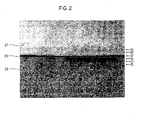
- a cross-sectional TEM image is shown in FIG. 2 .
- Each of "point” in Table 1 corresponds to the position indicated by each of arrows illustrated in FIG. 2 .
- the thickness of the diffusion barrier layer was 3.0 nm.
- Table 1 Point Al (atomic %) Si (atomic %) Ge (atomic %) 1 97.6 1.8 0.6 2 97.2 2.2 0.6 3 51.6 24.9 23.5 4 3.0 96.2 0.8 5 2.1 97.5 0.4 6 1.5 98.2 0.3
- the diffusion barrier layer 23 may be considered a solid layer formed by Si - Ge bond of covalent nature, by aggregation of Ge contained in the Al alloy film to the interface of the semiconductor region from a very initial stage of a heat treatment. If there was an interface where Al and Si are in direct contact with each other even partially during the heat treatment, the diffusion should have occurred as the diffusion rates of Al and Si are very high. By the fact that no trace of such diffusion was observed, it can be considered that a diffusion barrier layer was formed from a very initial stage of a heat treatment, Ge is incrassated at the interface between Al and Si once it is subjected to a heat treatment, and that Ge or Ge - Si bonds play the role of diffusion prevention.
- the semiconductor element of the present invention is preferably used for the MOS type semiconductor elements such as IGBT and power MOSFET.
Landscapes
- Electrodes Of Semiconductors (AREA)
Abstract
Description
- The present invention related to a semiconductor element and a method for manufacturing a semiconductor element.
- Recent years, insulated-gate (MOS) type semiconductor elements are widely used for power device which control large electric power. Examples of the MOS type semiconductor elements are such as IGBT (insulated gate bipolar transistor) and power MOSFET (power metal-oxide semiconductor field-effect transistor).
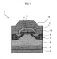
- A general configuration of an IGBT as a typical MOS type semiconductor is explained hereinafter by referring to
FIG. 1 . An IGBT 1 illustrated inFIG. 1 comprises a p-type collector layer 2, an n-type base layer 3 fabricated on thecollector layer 2, a p-type body region 4 fabricated in a spatially-segregated manner on the surface of thebase layer 3, and an n-type emitter layer 5 fabricated on the surface of each of the body region. Thecollector layer 2, thebase layer 3, the body region 4, and theemitter layer 5 are usually fabricated within the body of a substrate. Acollector electrode 6 is connected to thecollector layer 2. Within thebase layer 3, a region of the n-type base layer configured in between twoemitter layers 5 is a channel region 7. The IGBT 1 further has agate insulating film 8 and agate electrode 9 fabricated on the surface of the channel region 7 in that order. On a surface of theemitter layer 5, anemitter electrode 10 is also fabricated. Theemitter electrode 10 and thegate electrode 9 are electrically insulated from each other by an interlayerdielectric film 11. Thecollector electrode 6 is directly fixed by a soldering layer and electrically connected to a circuit board or the like. Connected to the surface of theemitter electrode 10 are metal wires and ribbons through which the electrode is electrically connected with external terminal. An Al-based electrode comprising pure Al or an Al alloy is used for electrodes such as thecollector electrode 6 and others. - N-type semiconductor regions such as
base layer 3 andemitter layer 5, and p-type such ascollector layer 2 and body region 4 in IGBT 1 are fabricated for example by ion-implantation of elements such as phosphorus (P), arsenic (As), and B (boron) in a substrate comprising Si, followed by a heat treatment for activation. The ion-implantation is conducted at certain dose amount, acceleration voltage, and implantation angle prescribed for each of the regions, followed by activation heat treatment at temperatures and durations predetermined for each of the regions. Specifically, in the manufacturing process of the IGBT 1, for example an ion-implantation is carried out to thecollector layer 2 from the back side of the substrate after fabricating anemitter electrode 10 on the surface of the substrate. Subsequently, activation of the implanted ions is promoted by carrying out a heat treatment at 450 °C or lower. In a case where an electrical connection through a soldering layer is included, the device may be heated to about 250 °C for a reflow process. - In such a manufacturing process, the higher the temperature of the heat treatment, the more the interdiffusion of atoms is enhanced across an interface between an electrode and a silicon semiconductor region adjacent with each other. Occasionally used for the electrode to prevent the interdiffusion is an Al - Si alloy in which silicon of one to a few percent is contained. However, even if such an alloy is used, the aforementioned interdiffusion cannot be circumvented for a heat treatment at 450 °C or higher temperatures. Patent literature 1, for example, describes a heat treatment at 800 °C to 950 °C for the purpose of activation of a collector layer. The heat treatment at such high temperatures, however, is restricted to be conducted prior to fabricating an electrode. Once an electrode is fabricated, the heat treatment is carried out up to about 450 °C, and no description is found in the literature referring to heat treatment at higher temperatures.
- As described above, when a heat treatment to activate collector layer is conducted for devices on which an Al-based film is deposited, the heat treatment at 450 °C or above causes interdiffusion of atoms between an electrode and Si in contact with each other. In case the heat treatment is conducted at relatively low temperatures, other kinds of problems such as prolonged period of time of several hours to activate the collector layer and insufficient activation of the implanted ions may arise.
- As a technology to suppress the interdiffusion,
patent literature 2 discloses an approach to insert a nitride layer as a diffusion barrier layer at the interface of an Al-base electrode with a semiconductor region. The nitride layer comprising insulating SiN or AIN or the like causes an increase in contact resistance and electrical power loss. It is possible to reduce the contact resistance to some extent by for example a thin the nitride layer up to 10 nm or less so as to exert the tunneling effect or the like. It is, however, of limited effectiveness because the nitride is inherently an insulator. Moreover, the thinner the nitride layer, the more the interdiffusion. The suppression of the thermal diffusion and contact resistance are in a tradeoff relation. In order to put the approach in practice, it is thus necessary to precisely control the thickness of the nitride layer in a well-balanced manner, which is, however, extremely difficult in reality. -
- Patent literature 1: Japanese Patent Application Publication No.
2007-242699 - Patent literature 2: Japanese Patent Application Publication No.
2008-10801 - The present invention has been made in light of the circumstances described above. It is an object of the present invention to provide a semiconductor element and a method for manufacturing the semiconductor element in which interdiffusion of atoms between a semiconductor region and an electrode is suppressed and rise of the contact resistance is avoided even when the semiconductor element is exposed to a high temperature during fabrication process or others.
- The present invention provides a semiconductor element and a method for manufacturing a semiconductor element described below.
- (1) A semiconductor element comprising
a semiconductor region including silicon,
an electrode including aluminum, and
a diffusion barrier layer including germanium between the semiconductor region and the electrode;
wherein an amount of germanium contained in at least a part of the diffusion barrier layer is 4 atomic percent or more.
In the semiconductor element, interdiffusion of atoms between a semiconductor region and an electrode is suppressed by the presence of a diffusion barrier including a given amount of germanium between a semiconductor region and an electrode. Moreover, in the semiconductor element, because of the presence of the diffusion barrier, rise of the contact resistance is avoided due to the presence of the diffusion barrier layer which comprises semiconductor germanium. - (2) A semiconductor according to (1) wherein;
an amount of germanium contained in at least a part of the diffusion barrier layer is 4 atomic percent or more and 50 atomic percent or less, and
a thickness of the diffusion barrier layer is 0.5 nm or more and 100 nm or less. By controlling the amount of germanium contained in at least a part of the diffusion barrier layer and its thickness within the range, excellent diffusion barrier property can be exerted while keeping the production cost low. - (3) A semiconductor according to (2) wherein;
- an amount of germanium contained in at least a part of the diffusion barrier layer is 20 atomic percent or more and 30 atomic percent or less, and
- a thickness of the diffusion barrier layer is 1 nm or more and 5 nm or less. By controlling the amount of germanium contained in at least a part of the diffusion barrier layer and its thickness within the above-mentioned range, the effects can be enhanced.
- (4) A manufacturing method of a semiconductor element according to any one of (1) to (3) comprising a process to fabricate an aluminum alloy film which contains germanium on a surface of a semiconductor region comprising silicon, and
a process to conduct a heat treatment to the semiconductor region on which the aluminum alloy film is fabricated. - (5) A manufacturing method of a semiconductor element according to (4) wherein an amount of germanium contained in the aluminum alloy film is 0.1 atomic % or more and 3 atomic % or less, and the temperature of the heat treatment is 300 °C or higher and 600 °C or lower.
A diffusion barrier layer including germanium is formed between the semiconductor region and the aluminum alloy film via the heat treatment in the manufacturing method. It becomes possible to suppress interdiffusion of atoms between the semiconductor region and the aluminum alloy film (electrode) during the heat treatment or the like, accordingly. - (6) A semiconductor element obtained by the fabrication method according to (4) or (5)
- In the semiconductor obtained by the fabrication methods, interdiffusion of atoms between a semiconductor region and an aluminum alloy film (electrode) is suppressed and rise of the contact resistance is avoided even with the presence of the diffusion barrier layer.
- The contained amount of each element (atomic percent) is data acquired by elemental analysis using energy dispersive X-ray analysis (EDX). A "part" of the diffusion barrier layer means a field of measurement in the analysis. The thickness of the diffusion barrier layer is an average value of those measured at arbitrary 5 points by using a transmission electron microscope (TEM).
- As explained hereinbefore, in a semiconductor element according to the present invention, interdiffusion of atoms between a semiconductor region and an electrode is suppressed and rise of the contact resistance is avoided even when the semiconductor element is subjected to high temperature. The semiconductor element may be preferably used for MOS type semiconductor elements or the like, accordingly. Further, the semiconductor element may be efficiently fabricated by the manufacturing method.
-
- [
FIG. 1 ] A schematic cross-sectional view of a common IGBT. - [
FIG. 2 ] A cross-sectional TEM micrograph depicting an interface between a semiconductor region and an electrode in a semiconductor element of an example. - Described in detail hereinafter are embodiments of a semiconductor element and a method for manufacturing the semiconductor element according to the present invention.
- The semiconductor element according to the present invention comprises a semiconductor region, an electrode, and a diffusion barrier layer between the semiconductor region and the electrode.
- The semiconductor region includes silicon. The semiconductor region generally comprises a known semiconductor material such as silicon substrate and silicon carbide substrate, and the like, which contains silicon as a main constituent. The semiconductor region may include phosphorus, arsenic, boron, and so on in addition to silicon. In such a case, the amount of phosphorus, arsenic, boron, and the like is preferably in the range from 1016 /cm3 to 1019 /cm3.
- The electrode is in contact with the semiconductor region via the diffusion barrier layer. The electrode is electrically connected to the semiconductor region because the diffusion barrier layer is not insulating as described hereinafter in detail.
- The electrode includes aluminum as a main constituent. Generally-known pure aluminum and aluminum alloys may be used for the electrode. As the alloy element is not specifically limited, it may be silicon, copper, nitrogen, and rare-earth elements such as neodymium and yttrium. If silicon is included as an alloy element, the amount of silicon is preferably in the range from 0.5 to 1.0 atomic percent. If copper is included as an alloy element, the amount is preferably in the range from 0.1 to 0.5 atomic percent. If rare-earth group element is included as an alloy element, the amount is preferably in the range from 0.2 to 2.0 atomic percent.
- The diffusion barrier layer lies between a semiconductor region and an electrode as described above. Specifically, if for example the semiconductor region is a collector layer and the electrode is a collector electrode which is electrically connected to the collector layer, the diffusion barrier layer lies between the collector layer and the collector electrode. Further, of the semiconductor region is an emitter layer and the electrode is an emitter electrode which is electrically connected to the emitter layer, the diffusion barrier layer lies between the emitter layer and the emitter electrode.
- The diffusion barrier layer contains germanium. According to the semiconductor element which contains a diffusion barrier layer including germanium, interdiffusion of atoms between a semiconductor region and an electrode may be suppressed even when the semiconductor element is subjected to high temperature exceeding for example 450 °C.
- Here, germanium is a semiconductor material having electrical resistivity of about 70 µΩcm at room temperature, which is close to those of metals. Therefore, even in a case where the diffusion barrier layer was consisting of only germanium, the contact resistance may be significantly reduced as compared to cases where the diffusion barrier comprises a conventional insulating material such as SiN. Moreover, due to the presence of the diffusion barrier comprising germanium in the semiconductor element, Si - Ge chemical bonds having covalent nature may be formed with silicon and germanium in the semiconductor region. As Si - Ge is a semiconductor, once being subjected to thermal process, aluminum of the electrode is naturally doped as an acceptor, and electrical resistance of the diffusion barrier layer is reduced.
- According to the semiconductor element which contains a diffusion barrier layer including germanium, the contact resistance can be reduced as compared to those having a conventional diffusion barrier layer, regardless of whether the diffusion barrier layer comprises of only germanium or it contains other element such as for example silicon or others. The contact resistance is not particularly dependent on thickness of the diffusion barrier layer. It is thus not very necessary to precisely control the thickness of the diffusion barrier layer according to the semiconductor element. The control condition of the fabrication process may be relaxed, which makes the formation of the diffusion barrier layer easier.
- The lower limit of an amount of germanium contained in at least a part of the diffusion barrier layer is preferably 4 atomic percent or more, and preferably 20 atomic percent or more. The diffusion barrier layer can offer sufficient diffusion prevention performance by controlling the contained amount of germanium higher than the lower limit.
- The upper limit of an amount of contained germanium is not specifically limited. It is preferably 50 atomic percent, and more preferably 30 atomic percent, considering cost and other factors. It may be considered that stoichiometrically and substantially sufficient Si - Ge bonds are formed, adequate performance of diffusion prevention and low electrical resistance may be obtained even the amount of germanium is below the upper limit.
- The diffusion barrier layer may comprise silicon and aluminum in addition to germanium.
- The lower limit of the amount of germanium contained in at least a part of the diffusion barrier layer is preferably 4 atomic percent, and more preferably 20 atomic percent in the case which the diffusion barrier layer contains silicon. The upper limit in such case on the other hand is preferably 50 atomic percent, and more preferably 30 atomic percent. Further, the ratio of the amount of silicon to the amount of germanium in the part of the diffusion barrier layer is preferably 0.3 or more and 3 or less, and more preferably 0.5 or more and 2 or less. By controlling the amount of silicon contained in the diffusion barrier layer, sufficient Si - Ge bonding may be formed in the diffusion barrier layer, enhance the diffusion prevention property while suppressing the electrical resistance.
- The lower limit of thickness of the diffusion barrier layer is preferably 0.5 nm, and more preferably 1 nm. The diffusion barrier layer can offer sufficient diffusion prevention performance by controlling the thickness larger than the lower limit.
- If the thickness of the diffusion barrier layer is 1 nm or more and the amount of germanium contained in at least a part of the diffusion barrier layer is 20 atomic percent or more, the diffusion barrier shows near-flawless performance even if it is subjected to a heat treatment at for example 500 °C for 20 minutes.
- The upper limit of thickness of the diffusion barrier layer is not specifically limited. It is preferably 100 nm, and more preferably 5 nm, considering cost and other factors.
- In a semiconductor element according to the present invention, interdiffusion of atoms between a semiconductor region and an electrode is suppressed and rise of the contact resistance is avoided even when the semiconductor element is subjected to high temperature. Therefore, by utilizing the present invention, a heat treatment for ion activation of a collector layer or the like may be conducted at 450 °C or higher temperatures during a fabrication process of, for example, IGBT. A heat treatment at such high temperatures shortens the process time and reduce the manufacturing cost. Further, according to the semiconductor element, the activation rate of the dopant which is ion-implanted to the collector layer or the like is enhanced by the high-temperature heat treatment, resulting in improved performance of the device. Furthermore, according to the semiconductor element, it is possible to suppress interdiffusion of atoms even in a case where a surge current is induced for some reasons during operation and the Joule heat induced soaring temperature locally, and the reliability is enhanced as an irreversible destruction is less likely to occur.
- The manufacturing method of the semiconductor element is not particularly limited, and may comprise;
- (1) a process to fabricate an aluminum alloy film which contains germanium on a surface of a semiconductor region comprising silicon, and
a process to conduct a heat treatment to the semiconductor region on which the aluminum alloy film is fabricated.
The manufacturing method may comprise; - (2) a process to fabricate a diffusion barrier layer on the surface of a semiconductor region comprising silicon by using sputtering or the like, and
a process to fabricate a pure aluminum or an aluminum alloy film on the surface of the diffusion barrier layer.
The pure aluminum or aluminum alloy film works as an electrode of the fabricated semiconductor element. - Among these manufacturing methods, the method described as (1) is preferred. Germanium of an aluminum alloy film precipitates or incrassates at an interface by a heat treatment in the manufacturing method (1). A diffusion barrier comprising germanium is thereby formed between an semiconductor region and an aluminum alloy film during a heat treatment. Interdiffusion of atoms between the semiconductor region and the aluminum alloy film during the heat treatment and the like may be suppressed accordingly. Moreover, according to the manufacturing method (1), thickness of the formed diffusion barrier layer can be readily controlled by the amount of germanium contained in the aluminum alloy film. In such a case, formation of a thin diffusion barrier layer of 5 nm in thickness, for example, can be conducted relatively easily while suppressing used amount of costly germanium.
- In the semiconductor element obtained by the method for manufacturing the semiconductor element of the present invention, interdiffusion of atoms between a semiconductor region and an electrode is suppressed and rise of the contact resistance is avoided even with the presence of the diffusion barrier layer.
- The present invention does not limit the method of deposition of the Al alloy film. For example, publicly known method such as sputtering and evaporation may be used.
- The amount of germanium contained in the Al alloy film is not specifically limited. It may be, for example, set as 0.1 atomic percent or more and 3 atomic percent or less.
- The method of the heat treatment is not particularly limited, and heretofore known method may be adopted. The heat treatment may be conducted as an activation process after an ion-implantation to a semiconductor region, or may be conducted independently.
- Temperature and duration of the heat treatment are not particularly limited. As for the temperature, it may be set, for example, to a range of 300 °C or higher and 600 °C or lower, preferably 450 °C or higher and 550 °C or lower. As for the duration, it may be set, for example, to a range of 5 minutes or longer and 1 hour or shorter, preferably 30 minutes or longer and 1 hour or shorter.
- Meanwhile, other than the above-described process such as for example ion-implantation, a publicly known method may be adopted for the fabrication of the semiconductor element.
- The present invention is more specifically described below by presenting examples. The present invention is not limited to these examples described below.
- Amount of each composition and thickness of the diffusion barrier of the obtained semiconductor were measured using methods described below.
- Amount of each composition was determined by EDX line analyses. For the ED line analyses, a field emission transmission electron microscope (FE-TEM) (HF-2000 supplied by Hitachi, Ltd.) and an EDX analysis device (Sigma supplied by Kevex Corp.) attached to the FE-TEM were used. Measurement data were acquired at points at intervals of approximately 5nm for the EDX line analyses.
- It is noted that while the diameter of incident electron beam in the used microscope is about 1 - 2 nm, it spreads about due to electron beam scattering in the specimen and the detection area expands. In addition, a margin of error of approximately 10 % is inherent in the semi-quantitative evaluation of EDX analyses. Therefore, absolute value of the amount of each composition should be interpreted with an attention to the fact that it has not only an aspect of absolute value of measured data but also relative significance of the line analyses data.
- By using a field emission transmission electron microscope (FE-TEM) (HF-2000 supplied by Hitachi, Ltd.), thicknesses of the diffusion barrier layer were measured at arbitrary 5 points, and their average value was calculated.
- On the surface of a monocrystalline silicon substrate with (100) plane direction as the semiconductor region, an aluminum alloy film containing 0.5 atomic percent germanium was deposited by magnetron sputtering. A heat treatment was subsequently conducted at 500 °C for 20 minutes in an inert gas (N2) atmosphere. In this way, a diffusion barrier layer was formed between the silicon substrate (semiconductor region) and the aluminum alloy film (electrode) to obtain a semiconductor element of example 1.
- Amount of each composition and thickness of the diffusion barrier layer of the obtained semiconductor were measured using methods described above. The amount of each composition is shown in Table 1. A cross-sectional TEM image is shown in
FIG. 2 . Each of "point" in Table 1 corresponds to the position indicated by each of arrows illustrated inFIG. 2 . The thickness of the diffusion barrier layer was 3.0 nm.Table 1 Point Al (atomic %) Si (atomic %) Ge (atomic %) ① 97.6 1.8 0.6 ② 97.2 2.2 0.6 ③ 51.6 24.9 23.5 ④ 3.0 96.2 0.8 ⑤ 2.1 97.5 0.4 ⑥ 1.5 98.2 0.3 - As shown in the cross-sectional TEM picture of
FIG. 2 , it was confirmed that adiffusion barrier 23 was formed between an electrode 21 (Al) and a semiconductor region 22 (Si). Interdiffusion of Al and Si was not observed. - The
diffusion barrier layer 23 may be considered a solid layer formed by Si - Ge bond of covalent nature, by aggregation of Ge contained in the Al alloy film to the interface of the semiconductor region from a very initial stage of a heat treatment. If there was an interface where Al and Si are in direct contact with each other even partially during the heat treatment, the diffusion should have occurred as the diffusion rates of Al and Si are very high. By the fact that no trace of such diffusion was observed, it can be considered that a diffusion barrier layer was formed from a very initial stage of a heat treatment, Ge is incrassated at the interface between Al and Si once it is subjected to a heat treatment, and that Ge or Ge - Si bonds play the role of diffusion prevention. - While the present invention has been described in detail above with references to specific embodiments thereof, it will be apparent to one with skill in the art that various changes and modifications may be made without departing from the spirit and scope of the present invention.
- This application claims the benefit of Japanese Patent Application No.
2011-157571 filed July 19, 2011 - The semiconductor element of the present invention is preferably used for the MOS type semiconductor elements such as IGBT and power MOSFET.
-
- 1
- IGBT
- 2
- Collector layer
- 3
- Base layer
- 4
- Body region
- 5
- Emitter layer
- 6
- Collector electrode
- 7
- Channel region
- 8
- Gate insulating film
- 9
- Gate electrode film
- 10
- Emitter electrode
- 11
- Interlayer dielectric film
- 21
- Electrode (Al)
- 22
- Semiconductor region (Si)
- 23
- Diffusion barrier layer
Claims (6)
- A semiconductor element comprising
a semiconductor region including silicon,
an electrode including aluminum, and
a diffusion barrier layer including germanium between the semiconductor region and the electrode;
wherein an amount of germanium contained in at least a part of the diffusion barrier layer is 4 atomic percent or more. - A semiconductor according to Claim 1 wherein;
an amount of germanium contained in at least a part of the diffusion barrier layer is 4 atomic percent or more and 50 atomic percent or less, and
a thickness of the diffusion barrier layer is 0.5 nm or more and 100 nm or less. - A semiconductor according to Claim 2 wherein;
an amount of germanium contained in at least a part of the diffusion barrier layer is 20 atomic percent or more and 30 atomic percent or less, and
a thickness of the diffusion barrier layer is 1 nm or more and 5 nm or less. - A manufacturing method of a semiconductor element according to any one of Claims 1 to 3 comprising;
a process step to form an aluminum alloy comprising germanium on a surface of semiconductor region containing silicon, and
a process step to conduct a heat treatment of the semiconductor region on which the aluminum alloy is formed. - A manufacturing method of a semiconductor element according to Claims 4 wherein;
an amount of germanium contained in the aluminum alloy film is 0.1 atomic % or more and 3 atomic % or less, and
the temperature of the heat treatment is 300 °C or higher and 600 °C or lower. - A semiconductor element fabricated by the method according to Claim 4.
Applications Claiming Priority (2)
| Application Number | Priority Date | Filing Date | Title |
|---|---|---|---|
| JP2011157571A JP5303008B2 (en) | 2011-07-19 | 2011-07-19 | Semiconductor device and method for manufacturing semiconductor device |
| PCT/JP2012/068383 WO2013012050A1 (en) | 2011-07-19 | 2012-07-19 | Semiconductor element and method for manufacturing semiconductor element |
Publications (3)
| Publication Number | Publication Date |
|---|---|
| EP2741318A1 true EP2741318A1 (en) | 2014-06-11 |
| EP2741318A4 EP2741318A4 (en) | 2015-03-25 |
| EP2741318B1 EP2741318B1 (en) | 2020-08-26 |
Family
ID=47558225
Family Applications (1)
| Application Number | Title | Priority Date | Filing Date |
|---|---|---|---|
| EP12815245.1A Not-in-force EP2741318B1 (en) | 2011-07-19 | 2012-07-19 | Semiconductor element and method for manufacturing semiconductor element |
Country Status (7)
| Country | Link |
|---|---|
| US (1) | US20140151886A1 (en) |
| EP (1) | EP2741318B1 (en) |
| JP (1) | JP5303008B2 (en) |
| KR (1) | KR101541656B1 (en) |
| CN (1) | CN103733310B (en) |
| TW (1) | TWI493706B (en) |
| WO (1) | WO2013012050A1 (en) |
Family Cites Families (13)
| Publication number | Priority date | Publication date | Assignee | Title |
|---|---|---|---|---|
| JPH065734B2 (en) * | 1985-09-28 | 1994-01-19 | 新日本無線株式会社 | Semiconductor device |
| JP2730265B2 (en) * | 1990-05-14 | 1998-03-25 | 日本電気株式会社 | Semiconductor device and manufacturing method thereof |
| JPH04280424A (en) * | 1991-03-07 | 1992-10-06 | Hitachi Ltd | Semiconductor wiring structure and its manufacture |
| JP3804945B2 (en) * | 1996-04-29 | 2006-08-02 | 株式会社半導体エネルギー研究所 | Method for manufacturing thin film transistor |
| US6607948B1 (en) * | 1998-12-24 | 2003-08-19 | Kabushiki Kaisha Toshiba | Method of manufacturing a substrate using an SiGe layer |
| JP2001185571A (en) * | 1999-12-22 | 2001-07-06 | Matsushita Electronics Industry Corp | Method and apparatus for forming bump electrode |
| JP3940385B2 (en) * | 2002-12-19 | 2007-07-04 | 株式会社神戸製鋼所 | Display device and manufacturing method thereof |
| JP2008010801A (en) | 2005-08-17 | 2008-01-17 | Kobe Steel Ltd | Source/drain electrode, thin-film transistor substrate and manufacture method thereof, and display device |
| JP4826290B2 (en) | 2006-03-06 | 2011-11-30 | トヨタ自動車株式会社 | Manufacturing method of semiconductor device |
| JP2010238800A (en) * | 2009-03-30 | 2010-10-21 | Kobe Steel Ltd | Al ALLOY FILM FOR DISPLAY, THIN FILM TRANSISTOR SUBSTRATE AND DISPLAY |
| CN101599522B (en) * | 2009-06-30 | 2011-05-25 | 厦门市三安光电科技有限公司 | Vertical LED adopting insulating medium barrier layer and preparation method thereof |
| JP2011035153A (en) * | 2009-07-31 | 2011-02-17 | Kobe Steel Ltd | Thin-film transistor substrate and display device |
| US8536043B2 (en) * | 2011-01-31 | 2013-09-17 | International Business Machines Corporation | Reduced S/D contact resistance of III-V MOSFET using low temperature metal-induced crystallization of n+ Ge |
-
2011
- 2011-07-19 JP JP2011157571A patent/JP5303008B2/en not_active Expired - Fee Related
-
2012
- 2012-07-19 CN CN201280035317.8A patent/CN103733310B/en not_active Expired - Fee Related
- 2012-07-19 WO PCT/JP2012/068383 patent/WO2013012050A1/en not_active Ceased
- 2012-07-19 KR KR1020147001064A patent/KR101541656B1/en not_active Expired - Fee Related
- 2012-07-19 US US14/233,388 patent/US20140151886A1/en not_active Abandoned
- 2012-07-19 EP EP12815245.1A patent/EP2741318B1/en not_active Not-in-force
- 2012-07-19 TW TW101126047A patent/TWI493706B/en not_active IP Right Cessation
Also Published As
| Publication number | Publication date |
|---|---|
| JP5303008B2 (en) | 2013-10-02 |
| US20140151886A1 (en) | 2014-06-05 |
| TW201330252A (en) | 2013-07-16 |
| CN103733310A (en) | 2014-04-16 |
| JP2013026308A (en) | 2013-02-04 |
| KR20140024460A (en) | 2014-02-28 |
| WO2013012050A1 (en) | 2013-01-24 |
| CN103733310B (en) | 2016-08-17 |
| EP2741318A4 (en) | 2015-03-25 |
| EP2741318B1 (en) | 2020-08-26 |
| TWI493706B (en) | 2015-07-21 |
| KR101541656B1 (en) | 2015-08-03 |
Similar Documents
| Publication | Publication Date | Title |
|---|---|---|
| US8722487B2 (en) | Semiconductor device with an electrode including an aluminum-silicon film | |
| JP5646527B2 (en) | Semiconductor device and manufacturing method of semiconductor device | |
| JP6728096B2 (en) | Semiconductor device, method of manufacturing semiconductor device, inverter circuit, drive device, vehicle, and elevator | |
| US7936065B2 (en) | Semiconductor devices and method of manufacturing them | |
| EP2428983A1 (en) | Semiconductor device and method of producing same | |
| DE112013001297B4 (en) | Method for producing a power semiconductor device | |
| US20150008478A1 (en) | Semiconductor device and manufacturing method of the same | |
| JP7605241B2 (en) | Method for manufacturing a trench type semiconductor device | |
| JP2011151350A (en) | Semiconductor device manufacturing method and semiconductor device | |
| JP5160001B2 (en) | Manufacturing method of semiconductor device | |
| JP6728097B2 (en) | Semiconductor device, method of manufacturing semiconductor device, inverter circuit, drive device, vehicle, and elevator | |
| JP2009194197A (en) | Semiconductor device and manufacturing method thereof | |
| US9741805B2 (en) | Semiconductor device and method for manufacturing the semiconductor device | |
| EP2741318B1 (en) | Semiconductor element and method for manufacturing semiconductor element | |
| JP7844281B2 (en) | Semiconductor device and method for manufacturing a semiconductor device | |
| JP2015043458A (en) | Semiconductor device | |
| JP2009010421A (en) | Method of mounting a semiconductor device on a circuit board | |
| JP4768231B2 (en) | Manufacturing method of semiconductor device | |
| JP2006093206A (en) | SiC semiconductor device and method of manufacturing SiC semiconductor device | |
| JP7805861B2 (en) | Semiconductor device and manufacturing method thereof | |
| JP5445563B2 (en) | Manufacturing method of semiconductor device | |
| US20260101800A1 (en) | Semiconductor device and method of manufacturing semiconductor device | |
| JPWO2013099050A1 (en) | Silicon carbide semiconductor device manufacturing method, silicon carbide semiconductor device, and silicon carbide semiconductor module | |
| JP2011222584A (en) | Semiconductor device and manufacturing method thereof | |
| JPWO2020115838A1 (en) | Semiconductor devices and methods for manufacturing semiconductor devices |
Legal Events
| Date | Code | Title | Description |
|---|---|---|---|
| PUAI | Public reference made under article 153(3) epc to a published international application that has entered the european phase |
Free format text: ORIGINAL CODE: 0009012 |
|
| 17P | Request for examination filed |
Effective date: 20140103 |
|
| AK | Designated contracting states |
Kind code of ref document: A1 Designated state(s): AL AT BE BG CH CY CZ DE DK EE ES FI FR GB GR HR HU IE IS IT LI LT LU LV MC MK MT NL NO PL PT RO RS SE SI SK SM TR |
|
| RIN1 | Information on inventor provided before grant (corrected) |
Inventor name: YOKOTA, YOSHIHIRO Inventor name: OKUNO, HIROYUKI Inventor name: MAEDA TAKEAKI |
|
| RAP1 | Party data changed (applicant data changed or rights of an application transferred) |
Owner name: KABUSHIKI KAISHA KOBE SEIKO SHO (KOBE STEEL, LTD.) |
|
| RIN1 | Information on inventor provided before grant (corrected) |
Inventor name: YOKOTA, YOSHIHIRO Inventor name: OKUNO, HIROYUKI Inventor name: MAEDA TAKEAKI |
|
| DAX | Request for extension of the european patent (deleted) | ||
| A4 | Supplementary search report drawn up and despatched |
Effective date: 20150223 |
|
| RIC1 | Information provided on ipc code assigned before grant |
Ipc: H01L 21/768 20060101ALI20150217BHEP Ipc: H01L 29/78 20060101ALI20150217BHEP Ipc: H01L 21/28 20060101AFI20150217BHEP Ipc: H01L 29/161 20060101ALI20150217BHEP Ipc: H01L 21/285 20060101ALI20150217BHEP Ipc: H01L 29/165 20060101ALI20150217BHEP Ipc: H01L 29/45 20060101ALI20150217BHEP Ipc: H01L 23/532 20060101ALI20150217BHEP Ipc: H01L 29/739 20060101ALI20150217BHEP Ipc: H01L 29/40 20060101ALI20150217BHEP Ipc: H01L 29/768 20060101ALI20150217BHEP |
|
| 17Q | First examination report despatched |
Effective date: 20151111 |
|
| STAA | Information on the status of an ep patent application or granted ep patent |
Free format text: STATUS: EXAMINATION IS IN PROGRESS |
|
| GRAP | Despatch of communication of intention to grant a patent |
Free format text: ORIGINAL CODE: EPIDOSNIGR1 |
|
| STAA | Information on the status of an ep patent application or granted ep patent |
Free format text: STATUS: GRANT OF PATENT IS INTENDED |
|
| INTG | Intention to grant announced |
Effective date: 20200401 |
|
| GRAS | Grant fee paid |
Free format text: ORIGINAL CODE: EPIDOSNIGR3 |
|
| GRAA | (expected) grant |
Free format text: ORIGINAL CODE: 0009210 |
|
| STAA | Information on the status of an ep patent application or granted ep patent |
Free format text: STATUS: THE PATENT HAS BEEN GRANTED |
|
| AK | Designated contracting states |
Kind code of ref document: B1 Designated state(s): AL AT BE BG CH CY CZ DE DK EE ES FI FR GB GR HR HU IE IS IT LI LT LU LV MC MK MT NL NO PL PT RO RS SE SI SK SM TR |
|
| REG | Reference to a national code |
Ref country code: GB Ref legal event code: FG4D |
|
| REG | Reference to a national code |
Ref country code: CH Ref legal event code: EP |
|
| REG | Reference to a national code |
Ref country code: AT Ref legal event code: REF Ref document number: 1307189 Country of ref document: AT Kind code of ref document: T Effective date: 20200915 |
|
| REG | Reference to a national code |
Ref country code: IE Ref legal event code: FG4D |
|
| REG | Reference to a national code |
Ref country code: DE Ref legal event code: R096 Ref document number: 602012072017 Country of ref document: DE |
|
| REG | Reference to a national code |
Ref country code: LT Ref legal event code: MG4D |
|
| PG25 | Lapsed in a contracting state [announced via postgrant information from national office to epo] |
Ref country code: FI Free format text: LAPSE BECAUSE OF FAILURE TO SUBMIT A TRANSLATION OF THE DESCRIPTION OR TO PAY THE FEE WITHIN THE PRESCRIBED TIME-LIMIT Effective date: 20200826 Ref country code: LT Free format text: LAPSE BECAUSE OF FAILURE TO SUBMIT A TRANSLATION OF THE DESCRIPTION OR TO PAY THE FEE WITHIN THE PRESCRIBED TIME-LIMIT Effective date: 20200826 Ref country code: BG Free format text: LAPSE BECAUSE OF FAILURE TO SUBMIT A TRANSLATION OF THE DESCRIPTION OR TO PAY THE FEE WITHIN THE PRESCRIBED TIME-LIMIT Effective date: 20201126 Ref country code: GR Free format text: LAPSE BECAUSE OF FAILURE TO SUBMIT A TRANSLATION OF THE DESCRIPTION OR TO PAY THE FEE WITHIN THE PRESCRIBED TIME-LIMIT Effective date: 20201127 Ref country code: PT Free format text: LAPSE BECAUSE OF FAILURE TO SUBMIT A TRANSLATION OF THE DESCRIPTION OR TO PAY THE FEE WITHIN THE PRESCRIBED TIME-LIMIT Effective date: 20201228 Ref country code: NO Free format text: LAPSE BECAUSE OF FAILURE TO SUBMIT A TRANSLATION OF THE DESCRIPTION OR TO PAY THE FEE WITHIN THE PRESCRIBED TIME-LIMIT Effective date: 20201126 Ref country code: HR Free format text: LAPSE BECAUSE OF FAILURE TO SUBMIT A TRANSLATION OF THE DESCRIPTION OR TO PAY THE FEE WITHIN THE PRESCRIBED TIME-LIMIT Effective date: 20200826 Ref country code: SE Free format text: LAPSE BECAUSE OF FAILURE TO SUBMIT A TRANSLATION OF THE DESCRIPTION OR TO PAY THE FEE WITHIN THE PRESCRIBED TIME-LIMIT Effective date: 20200826 |
|
| REG | Reference to a national code |
Ref country code: NL Ref legal event code: MP Effective date: 20200826 |
|
| REG | Reference to a national code |
Ref country code: AT Ref legal event code: MK05 Ref document number: 1307189 Country of ref document: AT Kind code of ref document: T Effective date: 20200826 |
|
| PG25 | Lapsed in a contracting state [announced via postgrant information from national office to epo] |
Ref country code: PL Free format text: LAPSE BECAUSE OF FAILURE TO SUBMIT A TRANSLATION OF THE DESCRIPTION OR TO PAY THE FEE WITHIN THE PRESCRIBED TIME-LIMIT Effective date: 20200826 Ref country code: LV Free format text: LAPSE BECAUSE OF FAILURE TO SUBMIT A TRANSLATION OF THE DESCRIPTION OR TO PAY THE FEE WITHIN THE PRESCRIBED TIME-LIMIT Effective date: 20200826 Ref country code: RS Free format text: LAPSE BECAUSE OF FAILURE TO SUBMIT A TRANSLATION OF THE DESCRIPTION OR TO PAY THE FEE WITHIN THE PRESCRIBED TIME-LIMIT Effective date: 20200826 Ref country code: NL Free format text: LAPSE BECAUSE OF FAILURE TO SUBMIT A TRANSLATION OF THE DESCRIPTION OR TO PAY THE FEE WITHIN THE PRESCRIBED TIME-LIMIT Effective date: 20200826 Ref country code: IS Free format text: LAPSE BECAUSE OF FAILURE TO SUBMIT A TRANSLATION OF THE DESCRIPTION OR TO PAY THE FEE WITHIN THE PRESCRIBED TIME-LIMIT Effective date: 20201226 |
|
| PG25 | Lapsed in a contracting state [announced via postgrant information from national office to epo] |
Ref country code: RO Free format text: LAPSE BECAUSE OF FAILURE TO SUBMIT A TRANSLATION OF THE DESCRIPTION OR TO PAY THE FEE WITHIN THE PRESCRIBED TIME-LIMIT Effective date: 20200826 Ref country code: SM Free format text: LAPSE BECAUSE OF FAILURE TO SUBMIT A TRANSLATION OF THE DESCRIPTION OR TO PAY THE FEE WITHIN THE PRESCRIBED TIME-LIMIT Effective date: 20200826 Ref country code: EE Free format text: LAPSE BECAUSE OF FAILURE TO SUBMIT A TRANSLATION OF THE DESCRIPTION OR TO PAY THE FEE WITHIN THE PRESCRIBED TIME-LIMIT Effective date: 20200826 Ref country code: DK Free format text: LAPSE BECAUSE OF FAILURE TO SUBMIT A TRANSLATION OF THE DESCRIPTION OR TO PAY THE FEE WITHIN THE PRESCRIBED TIME-LIMIT Effective date: 20200826 Ref country code: CZ Free format text: LAPSE BECAUSE OF FAILURE TO SUBMIT A TRANSLATION OF THE DESCRIPTION OR TO PAY THE FEE WITHIN THE PRESCRIBED TIME-LIMIT Effective date: 20200826 |
|
| REG | Reference to a national code |
Ref country code: DE Ref legal event code: R097 Ref document number: 602012072017 Country of ref document: DE |
|
| PG25 | Lapsed in a contracting state [announced via postgrant information from national office to epo] |
Ref country code: AT Free format text: LAPSE BECAUSE OF FAILURE TO SUBMIT A TRANSLATION OF THE DESCRIPTION OR TO PAY THE FEE WITHIN THE PRESCRIBED TIME-LIMIT Effective date: 20200826 Ref country code: AL Free format text: LAPSE BECAUSE OF FAILURE TO SUBMIT A TRANSLATION OF THE DESCRIPTION OR TO PAY THE FEE WITHIN THE PRESCRIBED TIME-LIMIT Effective date: 20200826 Ref country code: ES Free format text: LAPSE BECAUSE OF FAILURE TO SUBMIT A TRANSLATION OF THE DESCRIPTION OR TO PAY THE FEE WITHIN THE PRESCRIBED TIME-LIMIT Effective date: 20200826 |
|
| PG25 | Lapsed in a contracting state [announced via postgrant information from national office to epo] |
Ref country code: SK Free format text: LAPSE BECAUSE OF FAILURE TO SUBMIT A TRANSLATION OF THE DESCRIPTION OR TO PAY THE FEE WITHIN THE PRESCRIBED TIME-LIMIT Effective date: 20200826 |
|
| PLBE | No opposition filed within time limit |
Free format text: ORIGINAL CODE: 0009261 |
|
| STAA | Information on the status of an ep patent application or granted ep patent |
Free format text: STATUS: NO OPPOSITION FILED WITHIN TIME LIMIT |
|
| PG25 | Lapsed in a contracting state [announced via postgrant information from national office to epo] |
Ref country code: IT Free format text: LAPSE BECAUSE OF FAILURE TO SUBMIT A TRANSLATION OF THE DESCRIPTION OR TO PAY THE FEE WITHIN THE PRESCRIBED TIME-LIMIT Effective date: 20200826 |
|
| 26N | No opposition filed |
Effective date: 20210527 |
|
| PG25 | Lapsed in a contracting state [announced via postgrant information from national office to epo] |
Ref country code: SI Free format text: LAPSE BECAUSE OF FAILURE TO SUBMIT A TRANSLATION OF THE DESCRIPTION OR TO PAY THE FEE WITHIN THE PRESCRIBED TIME-LIMIT Effective date: 20200826 |
|
| PGFP | Annual fee paid to national office [announced via postgrant information from national office to epo] |
Ref country code: GB Payment date: 20210623 Year of fee payment: 10 |
|
| PGFP | Annual fee paid to national office [announced via postgrant information from national office to epo] |
Ref country code: DE Payment date: 20210622 Year of fee payment: 10 |
|
| REG | Reference to a national code |
Ref country code: CH Ref legal event code: PL |
|
| PG25 | Lapsed in a contracting state [announced via postgrant information from national office to epo] |
Ref country code: MC Free format text: LAPSE BECAUSE OF FAILURE TO SUBMIT A TRANSLATION OF THE DESCRIPTION OR TO PAY THE FEE WITHIN THE PRESCRIBED TIME-LIMIT Effective date: 20200826 |
|
| REG | Reference to a national code |
Ref country code: BE Ref legal event code: MM Effective date: 20210731 |
|
| PG25 | Lapsed in a contracting state [announced via postgrant information from national office to epo] |
Ref country code: LI Free format text: LAPSE BECAUSE OF NON-PAYMENT OF DUE FEES Effective date: 20210731 Ref country code: CH Free format text: LAPSE BECAUSE OF NON-PAYMENT OF DUE FEES Effective date: 20210731 |
|
| PG25 | Lapsed in a contracting state [announced via postgrant information from national office to epo] |
Ref country code: LU Free format text: LAPSE BECAUSE OF NON-PAYMENT OF DUE FEES Effective date: 20210719 Ref country code: FR Free format text: LAPSE BECAUSE OF NON-PAYMENT OF DUE FEES Effective date: 20210731 |
|
| PG25 | Lapsed in a contracting state [announced via postgrant information from national office to epo] |
Ref country code: IE Free format text: LAPSE BECAUSE OF NON-PAYMENT OF DUE FEES Effective date: 20210719 Ref country code: BE Free format text: LAPSE BECAUSE OF NON-PAYMENT OF DUE FEES Effective date: 20210731 |
|
| REG | Reference to a national code |
Ref country code: DE Ref legal event code: R119 Ref document number: 602012072017 Country of ref document: DE |
|
| GBPC | Gb: european patent ceased through non-payment of renewal fee |
Effective date: 20220719 |
|
| PG25 | Lapsed in a contracting state [announced via postgrant information from national office to epo] |
Ref country code: HU Free format text: LAPSE BECAUSE OF FAILURE TO SUBMIT A TRANSLATION OF THE DESCRIPTION OR TO PAY THE FEE WITHIN THE PRESCRIBED TIME-LIMIT; INVALID AB INITIO Effective date: 20120719 Ref country code: GB Free format text: LAPSE BECAUSE OF NON-PAYMENT OF DUE FEES Effective date: 20220719 Ref country code: DE Free format text: LAPSE BECAUSE OF NON-PAYMENT OF DUE FEES Effective date: 20230201 Ref country code: CY Free format text: LAPSE BECAUSE OF FAILURE TO SUBMIT A TRANSLATION OF THE DESCRIPTION OR TO PAY THE FEE WITHIN THE PRESCRIBED TIME-LIMIT Effective date: 20200826 |
|
| PG25 | Lapsed in a contracting state [announced via postgrant information from national office to epo] |
Ref country code: MK Free format text: LAPSE BECAUSE OF FAILURE TO SUBMIT A TRANSLATION OF THE DESCRIPTION OR TO PAY THE FEE WITHIN THE PRESCRIBED TIME-LIMIT Effective date: 20200826 |
|
| PG25 | Lapsed in a contracting state [announced via postgrant information from national office to epo] |
Ref country code: TR Free format text: LAPSE BECAUSE OF FAILURE TO SUBMIT A TRANSLATION OF THE DESCRIPTION OR TO PAY THE FEE WITHIN THE PRESCRIBED TIME-LIMIT Effective date: 20200826 |
|
| PG25 | Lapsed in a contracting state [announced via postgrant information from national office to epo] |
Ref country code: MT Free format text: LAPSE BECAUSE OF FAILURE TO SUBMIT A TRANSLATION OF THE DESCRIPTION OR TO PAY THE FEE WITHIN THE PRESCRIBED TIME-LIMIT Effective date: 20200826 |