EP2741133A1 - Array substrate, liquid crystal display panel and method of repairing broken lines of liquid crystal display panel - Google Patents
Array substrate, liquid crystal display panel and method of repairing broken lines of liquid crystal display panel Download PDFInfo
- Publication number
- EP2741133A1 EP2741133A1 EP20120778191 EP12778191A EP2741133A1 EP 2741133 A1 EP2741133 A1 EP 2741133A1 EP 20120778191 EP20120778191 EP 20120778191 EP 12778191 A EP12778191 A EP 12778191A EP 2741133 A1 EP2741133 A1 EP 2741133A1
- Authority
- EP
- European Patent Office
- Prior art keywords
- line
- repair area
- data line
- breakpoint
- data
- Prior art date
- Legal status (The legal status is an assumption and is not a legal conclusion. Google has not performed a legal analysis and makes no representation as to the accuracy of the status listed.)
- Granted
Links
Images



Classifications
-
- G—PHYSICS
- G02—OPTICS
- G02F—OPTICAL DEVICES OR ARRANGEMENTS FOR THE CONTROL OF LIGHT BY MODIFICATION OF THE OPTICAL PROPERTIES OF THE MEDIA OF THE ELEMENTS INVOLVED THEREIN; NON-LINEAR OPTICS; FREQUENCY-CHANGING OF LIGHT; OPTICAL LOGIC ELEMENTS; OPTICAL ANALOGUE/DIGITAL CONVERTERS
- G02F1/00—Devices or arrangements for the control of the intensity, colour, phase, polarisation or direction of light arriving from an independent light source, e.g. switching, gating or modulating; Non-linear optics
- G02F1/01—Devices or arrangements for the control of the intensity, colour, phase, polarisation or direction of light arriving from an independent light source, e.g. switching, gating or modulating; Non-linear optics for the control of the intensity, phase, polarisation or colour
- G02F1/13—Devices or arrangements for the control of the intensity, colour, phase, polarisation or direction of light arriving from an independent light source, e.g. switching, gating or modulating; Non-linear optics for the control of the intensity, phase, polarisation or colour based on liquid crystals, e.g. single liquid crystal display cells
- G02F1/133—Constructional arrangements; Operation of liquid crystal cells; Circuit arrangements
- G02F1/1333—Constructional arrangements; Manufacturing methods
- G02F1/1343—Electrodes
-
- G—PHYSICS
- G02—OPTICS
- G02F—OPTICAL DEVICES OR ARRANGEMENTS FOR THE CONTROL OF LIGHT BY MODIFICATION OF THE OPTICAL PROPERTIES OF THE MEDIA OF THE ELEMENTS INVOLVED THEREIN; NON-LINEAR OPTICS; FREQUENCY-CHANGING OF LIGHT; OPTICAL LOGIC ELEMENTS; OPTICAL ANALOGUE/DIGITAL CONVERTERS
- G02F1/00—Devices or arrangements for the control of the intensity, colour, phase, polarisation or direction of light arriving from an independent light source, e.g. switching, gating or modulating; Non-linear optics
- G02F1/01—Devices or arrangements for the control of the intensity, colour, phase, polarisation or direction of light arriving from an independent light source, e.g. switching, gating or modulating; Non-linear optics for the control of the intensity, phase, polarisation or colour
- G02F1/13—Devices or arrangements for the control of the intensity, colour, phase, polarisation or direction of light arriving from an independent light source, e.g. switching, gating or modulating; Non-linear optics for the control of the intensity, phase, polarisation or colour based on liquid crystals, e.g. single liquid crystal display cells
- G02F1/133—Constructional arrangements; Operation of liquid crystal cells; Circuit arrangements
- G02F1/136—Liquid crystal cells structurally associated with a semi-conducting layer or substrate, e.g. cells forming part of an integrated circuit
- G02F1/1362—Active matrix addressed cells
- G02F1/136259—Repairing; Defects
-
- H—ELECTRICITY
- H10—SEMICONDUCTOR DEVICES; ELECTRIC SOLID-STATE DEVICES NOT OTHERWISE PROVIDED FOR
- H10P—GENERIC PROCESSES OR APPARATUS FOR THE MANUFACTURE OR TREATMENT OF DEVICES COVERED BY CLASS H10
- H10P74/00—Testing or measuring during manufacture or treatment of wafers, substrates or devices
- H10P74/23—Testing or measuring during manufacture or treatment of wafers, substrates or devices characterised by multiple measurements, corrections, marking or sorting processes
-
- G—PHYSICS
- G02—OPTICS
- G02F—OPTICAL DEVICES OR ARRANGEMENTS FOR THE CONTROL OF LIGHT BY MODIFICATION OF THE OPTICAL PROPERTIES OF THE MEDIA OF THE ELEMENTS INVOLVED THEREIN; NON-LINEAR OPTICS; FREQUENCY-CHANGING OF LIGHT; OPTICAL LOGIC ELEMENTS; OPTICAL ANALOGUE/DIGITAL CONVERTERS
- G02F1/00—Devices or arrangements for the control of the intensity, colour, phase, polarisation or direction of light arriving from an independent light source, e.g. switching, gating or modulating; Non-linear optics
- G02F1/01—Devices or arrangements for the control of the intensity, colour, phase, polarisation or direction of light arriving from an independent light source, e.g. switching, gating or modulating; Non-linear optics for the control of the intensity, phase, polarisation or colour
- G02F1/13—Devices or arrangements for the control of the intensity, colour, phase, polarisation or direction of light arriving from an independent light source, e.g. switching, gating or modulating; Non-linear optics for the control of the intensity, phase, polarisation or colour based on liquid crystals, e.g. single liquid crystal display cells
- G02F1/133—Constructional arrangements; Operation of liquid crystal cells; Circuit arrangements
-
- G—PHYSICS
- G02—OPTICS
- G02F—OPTICAL DEVICES OR ARRANGEMENTS FOR THE CONTROL OF LIGHT BY MODIFICATION OF THE OPTICAL PROPERTIES OF THE MEDIA OF THE ELEMENTS INVOLVED THEREIN; NON-LINEAR OPTICS; FREQUENCY-CHANGING OF LIGHT; OPTICAL LOGIC ELEMENTS; OPTICAL ANALOGUE/DIGITAL CONVERTERS
- G02F1/00—Devices or arrangements for the control of the intensity, colour, phase, polarisation or direction of light arriving from an independent light source, e.g. switching, gating or modulating; Non-linear optics
- G02F1/01—Devices or arrangements for the control of the intensity, colour, phase, polarisation or direction of light arriving from an independent light source, e.g. switching, gating or modulating; Non-linear optics for the control of the intensity, phase, polarisation or colour
- G02F1/13—Devices or arrangements for the control of the intensity, colour, phase, polarisation or direction of light arriving from an independent light source, e.g. switching, gating or modulating; Non-linear optics for the control of the intensity, phase, polarisation or colour based on liquid crystals, e.g. single liquid crystal display cells
- G02F1/133—Constructional arrangements; Operation of liquid crystal cells; Circuit arrangements
- G02F1/136—Liquid crystal cells structurally associated with a semi-conducting layer or substrate, e.g. cells forming part of an integrated circuit
- G02F1/1362—Active matrix addressed cells
- G02F1/1368—Active matrix addressed cells in which the switching element is a three-electrode device
-
- H—ELECTRICITY
- H10—SEMICONDUCTOR DEVICES; ELECTRIC SOLID-STATE DEVICES NOT OTHERWISE PROVIDED FOR
- H10H—INORGANIC LIGHT-EMITTING SEMICONDUCTOR DEVICES HAVING POTENTIAL BARRIERS
- H10H29/00—Integrated devices, or assemblies of multiple devices, comprising at least one light-emitting semiconductor element covered by group H10H20/00
- H10H29/10—Integrated devices comprising at least one light-emitting semiconductor component covered by group H10H20/00
- H10H29/14—Integrated devices comprising at least one light-emitting semiconductor component covered by group H10H20/00 comprising multiple light-emitting semiconductor components
- H10H29/142—Two-dimensional arrangements, e.g. asymmetric LED layout
-
- G—PHYSICS
- G02—OPTICS
- G02F—OPTICAL DEVICES OR ARRANGEMENTS FOR THE CONTROL OF LIGHT BY MODIFICATION OF THE OPTICAL PROPERTIES OF THE MEDIA OF THE ELEMENTS INVOLVED THEREIN; NON-LINEAR OPTICS; FREQUENCY-CHANGING OF LIGHT; OPTICAL LOGIC ELEMENTS; OPTICAL ANALOGUE/DIGITAL CONVERTERS
- G02F1/00—Devices or arrangements for the control of the intensity, colour, phase, polarisation or direction of light arriving from an independent light source, e.g. switching, gating or modulating; Non-linear optics
- G02F1/01—Devices or arrangements for the control of the intensity, colour, phase, polarisation or direction of light arriving from an independent light source, e.g. switching, gating or modulating; Non-linear optics for the control of the intensity, phase, polarisation or colour
- G02F1/13—Devices or arrangements for the control of the intensity, colour, phase, polarisation or direction of light arriving from an independent light source, e.g. switching, gating or modulating; Non-linear optics for the control of the intensity, phase, polarisation or colour based on liquid crystals, e.g. single liquid crystal display cells
- G02F1/133—Constructional arrangements; Operation of liquid crystal cells; Circuit arrangements
- G02F1/136—Liquid crystal cells structurally associated with a semi-conducting layer or substrate, e.g. cells forming part of an integrated circuit
- G02F1/1362—Active matrix addressed cells
- G02F1/136259—Repairing; Defects
- G02F1/136263—Line defects
-
- G—PHYSICS
- G02—OPTICS
- G02F—OPTICAL DEVICES OR ARRANGEMENTS FOR THE CONTROL OF LIGHT BY MODIFICATION OF THE OPTICAL PROPERTIES OF THE MEDIA OF THE ELEMENTS INVOLVED THEREIN; NON-LINEAR OPTICS; FREQUENCY-CHANGING OF LIGHT; OPTICAL LOGIC ELEMENTS; OPTICAL ANALOGUE/DIGITAL CONVERTERS
- G02F2201/00—Constructional arrangements not provided for in groups G02F1/00 - G02F7/00
- G02F2201/12—Constructional arrangements not provided for in groups G02F1/00 - G02F7/00 electrode
- G02F2201/122—Constructional arrangements not provided for in groups G02F1/00 - G02F7/00 electrode having a particular pattern
Definitions
- the present disclosure relates to an array substrate, a liquid crystal display panel comprising the array substrate and a broken-line repairing method thereof.
- a structure in which a data repair line is arranged on the periphery of the liquid crystal display panel is usually adopted in the prior art, so as to facilitate the repair of a data-line broken line.
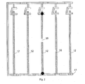
- FIG. 1 A normal pixel structure on an array substrate of the liquid crystal display panel is shown in FIG. 1 , and comprises: gate lines 11 and data lines 12, and pixel units 20 which are defined by the gate lines 11 and the data lines 12; a thin film transistor 13, a common electrode 14 and a pixel electrode 15 being formed in the pixel units 20. If one of the data lines in the liquid crystal display panel is a broken line, the data-line broken line may be repaired with reference to FIG. 2 . A specific procedure for the repair is as follows: both ends of the data-line broken line are connected, respectively, to a data repair line 41 by means of laser soldering, so as to achieve an object of repairing the data-line broken line.
- the above broken-line repairing method may be limited by the number of the data repair line.
- one data repair line or two data repair lines may be arranged in the liquid crystal display panel for repair of one data-line broken line or two data-line broken lines. If there are too many data-line broken lines in a liquid crystal display panel, the liquid crystal display panel may have to be discarded, to thereby affect the yield of a product.
- an array substrate comprising: signal lines, which includes a plurality of gate lines and a plurality of data lines intersecting with each other; and a plurality of pixel units defined by the gate lines and the data lines, wherein a thin film transistor, a common electrode and a pixel electrode which is connected to a drain of the thin film transistor, are formed in each of the pixel units, at the position of two corners in each of the pixel units which are adj acent to one of the data lines, a first repair area and a second repair area are formed, respectively; within the first repair area and the second repair area, patterns of the pixel electrode and the one of the data lines overlap, and there is no pattern of the common electrode.
- a third repair area is further formed; within the third repair area, patterns for the pixel electrode and the gate line overlap, and there is no pattern of the common electrode.
- a data repair line is formed around a pixel region comprising all of the pixel units; for the pixel unit, at the positions of two corners which are adjacent to another data line, a fourth repair area and a fifth repair area are further formed, respectively; within the fourth repair area and the fifth repair area, patterns for the pixel electrode and the said another data line overlap, and there is no pattern of the common electrode.
- a method for repairing a broken line for the signal lines comprising: a1, detecting and determining the position of a breakpoint for the signal lines; a2, when the breakpoint of a data line is detected, by means of laser soldering, the pixel electrode in the first repair area on one side of the breakpoint of the data line is connected to the data line, and the pixel electrode in the second repair area on another side of the breakpoint of the data line is connected to the data line; when the breakpoint of a gate line is detected, by means of laser soldering, the pixel electrode in the third repair area on one side of the breakpoint of the gate line is connected to the gate line, and the drain of the thin film transistor on another side of the breakpoint of the gate line is connected to the gate line.
- a method for repairing a broken line for the signal lines comprising: c1, detecting and determining the position of a breakpoint for the signal lines; c2, when the breakpoint of a data line is detected, by means of laser soldering, the pixel electrode in the first repair area on one side of the breakpoint of the data line is connected to the data line, and the pixel electrode in the second repair area on another side of the breakpoint of the data line is connected to the data line; alternatively, by means of laser soldering, the pixel electrode in the fourth repair area on one side of the breakpoint of the data line is connected to the data line, and the pixel electrode in the fifth repair area on another side of the breakpoint of the data line is connected to the data line; when the breakpoint of a gate line is detected, by means of laser soldering, a drain of a thin film transistor on one side of the breakpoint of the gate line is connected to the gate line; by means of laser cutting, a data line on another side
- the array substrate comprises: a plurality of gate lines 11 and a plurality of data lines 12 intersecting with each other (collectively called as signal lines), and a plurality of pixel units 20 defmed by the gate lines 11 and the data lines 12 (only one pixel unit is shown in the figure as an example).
- a thin film transistor 13, a common electrode 14 and a pixel electrode 15 which is connected to a drain of the thin film transistor 13 are formed in each of the pixel units 20.
- a first repair area 51 and a second repair area 52 are formed, respectively. Within the first repair area 51 and the second repair area 52, patterns of the pixel electrode 15 and the data line 12 overlap, and there is no pattern of the common electrode 14.
- the pixel electrode 15 and the data line 12 each are formed with protruding patterns, and the protruding patterns of the two overlap. That is, the pixel electrode 15 is formed with the protruding patterns protruding toward the data line 12, and the data line is formed with the protruding pattern protruding toward the pixel electrode 15, and the protruding patterns of the pixel electrode 15 and the protruding patterns of the data line 12 overlap.
- the thin film transistor within each pixel unit is located at a position adjacent to one corner of the pixel unit.
- a source of the thin film transistor is connected to a corresponding data line, and a gate of the thin film transistor is connected to a corresponding gate line, as shown in FIG. 3 .
- the pixel structure shown in FIG. 3 is described with reference to an example in which at the positions of two corners for the pixel unit 20 which are adjacent to one of data lines 12 on the right, the first repair area 51 and the second repair area 52 are formed.
- the pixel structure shown in FIG. 3 is not the unique case.
- a first repair area and a second repair area may be formed at the positions of two corners which are adjacent to one of data lines 12 on the left.
- a third repair area 53 is additionally formed. Within the third repair area 53, patterns for the pixel electrode 15 and the gate line 11 overlap, and there is no pattern of the common electrode 14.
- the pixel electrode 15 is formed with a protruding pattern protruding toward the gate line, and the protruding pattern and the pattern of the gate line overlap.
- the array substrate shown in FIG. 3 can only be used to repair a broken line for data lines 12, while an array substrate shown in FIG. 4 can be used to repair not only the broken line for data lines 12, but also a broken line for gate lines 11.
- an array substrate shown in FIG. 4 can be used to repair not only the broken line for data lines 12, but also a broken line for gate lines 11.
- methods for repairing the broken line for data lines 12 and the broken line for gate lines 11 are introduced, respectively.
- a method for repairing the broken line for data lines 12 with the array substrate shown in FIG. 3 it can also refer to the methods described below.
- step a2 the data line on top side of the breakpoint 30 of the data line is connected to the pixel electrode 15, and the data line on the lower side the breakpoint 30 of the data line is also connected to the pixel electrode 15, so that the broken line for data lines is repaired with the pixel electrode.
- step b2 the gate line on the left side of the breakpoint 30 of the gate line is connected to the drain of the thin film transistor, which is connected to the pixel electrode via a through hole, and the gate line on the right side of the breakpoint 30 of the gate line is also connected to the pixel electrode, so that the broken line for gate lines is repaired with the pixel electrode.
- the first repair area and the second repair area can be used to repair a data-line broken line
- the third repair area can be used to repair a gate-line broken line.
- the solutions provided by the present disclosure do not set a limit to the numbers of the data-line broken line and the gate-line broken line, and even if the number of the data-line broken line or the gate-line broken line is larger, they may be repaired one by one, thereby increasing the yield of the liquid crystal display panel.
- the array substrate comprises: a plurality of gate lines 11 and a plurality of data lines 12, and a plurality of pixel units 20 (two pixel units are shown in the figure as an example) defined by the gate lines 11 and the data lines 12.
- a thin film transistor 13, a common electrode 14 and a pixel electrode 15, which is connected to a drain of the thin film transistor 13, are formed in each of the pixel units 20.
- a first repair area 51 and a second repair area 52 are formed, respectively. Within the first repair area 51 and the second repair area 52, patterns of the pixel electrode 15 and the data line 12 overlap, and there is no pattern of the common electrode 14.
- the pixel electrode 15 and the data line 12 each are formed with protruding patterns, and the protruding patterns of the two overlap. That is, the.pixel electrode 15 is formed with the protruding patterns protruding toward the data line 12, and the data line is formed with the protruding patterns protruding toward the pixel electrode 15, and the protruding patterns of the pixel electrode 15 and the protruding patterns of the data line 12 overlap.
- a data repair line 41 is formed in the liquid crystal display panel.
- the wiring of the data repair line 41 can refer to FIG. 2 , and is not different from the wiring in the prior art.
- the data repair line can be formed around a pixel region comprising all the pixel units.
- a fourth repair area 54 and a fifth repair area 55 are additionally formed.
- patterns for the pixel electrode 15 and the said another data line 12 overlap, and there is no pattern of the common electrode 14.
- the pixel electrode 15 and the said another data line 12 each are formed with protruding patterns, and the protruding patterns of the two overlap. That is, the pixel electrode 15 is formed with the protruding patterns protruding toward the said another data line 12, and the said another data line is formed with the protruding patterns protruding toward the pixel electrode 15, and the protruding patterns of the pixel electrode 15 and the protruding patterns of the said another data line 12 overlap.
- the said one of data lines 12 is a data line on the right of the pixel unit 20, and the said another data line 12 is a data line on the left of the pixel unit 20.
- step c2 may alternatively be: by means of laser soldering, the pixel electrode 15 in the fourth repair area 54 on one side of the breakpoint of the data line 12 is connected to the data line 12, and the pixel electrode 15 in the fifth repair area 55 on another side of the breakpoint of the data line 12 is connected to the data line 12.
- this method for repairing the broken line for the data line 12 although positions for laser soldering during the reparation are not denoted in the figure, those skilled in the art can definitely find the positions for laser soldering from the above descriptions.
- step c2 the data lines on two sides of the breakpoint 30 of the data line are connected through the pixel electrode, thereby repairing the broken line for data lines.
- the pixel electrodes 15 in the two repair areas are connected to the data line 12, respectively, and a drain of a thin film transistor 13 (the thin film transistor in a pixel unit on the right in FIG. 9 ) is connected to the gate line 11;
- step d2 the gate lines on the two sides of the breakpoint 3 0 of the gate line are connected by using the pixel electrodes in two pixel units and a cut-off section of the data line between the two pixel units, and thus the broken line for gate lines can be repaired.
- a step d3 is also needed to repair the cut-off data line.
- the data line 12 is connected to the data repair line 41.
- FIG. 2 The details may refer to FIG. 2 , in which the two opposite ends of the cut-off data line 12 are connected, respectively, to the data repair line 41, so as to repair the cut-off data line.
- step d2 and the step d3 are arranged in a random order; and individual processes in the step d2 are also arranged in a random order.
- the first repair area and the second repair area can be used to repair a data-line broken line, and further, a gate-line broken line can be repaired in combination with the data repair line.
- the solutions provided by the present disclosure do not set a limit to the number of the data-line broken line, and even if the number of the data-line broken line or the gate-line broken line is larger, they may be repaired one by one, thereby increasing the yield of the liquid crystal display panel.
- a liquid crystal display panel which includes a color filter substrate and an array substrate facing each other and a liquid crystal layer interposed therebetween.
- Any array substrate according to embodiments of the present disclosure may be used for the array substrate.
- overlapping the pixel electrode and the data line or the gate line in a repair area means that there is an overlapping portion in a plan view taken along a surface of the array substrate, but that does not mean that the pixel electrode can directly contact with the data line or the gate line.
- the pixel electrode, the data line and the gate line is usually formed in different layers, and an insulating layer (a gate insulating film or a passivation layer) is interposed between the different layers.
- an insulating layer a gate insulating film or a passivation layer
- TN Twisted Nematic
- VA Vertical Alignment
- IPS In-Plain Switch
- FFS Fringe Field Switch
Landscapes
- Physics & Mathematics (AREA)
- Nonlinear Science (AREA)
- Mathematical Physics (AREA)
- Chemical & Material Sciences (AREA)
- Crystallography & Structural Chemistry (AREA)
- General Physics & Mathematics (AREA)
- Optics & Photonics (AREA)
- Engineering & Computer Science (AREA)
- Microelectronics & Electronic Packaging (AREA)
- Liquid Crystal (AREA)
- Devices For Indicating Variable Information By Combining Individual Elements (AREA)
Abstract
Description
- The present disclosure relates to an array substrate, a liquid crystal display panel comprising the array substrate and a broken-line repairing method thereof.
- In the course of manufacturing a liquid crystal display panel, repairing broken lines is an important means of enhancing the yield. A structure in which a data repair line is arranged on the periphery of the liquid crystal display panel is usually adopted in the prior art, so as to facilitate the repair of a data-line broken line.
- A normal pixel structure on an array substrate of the liquid crystal display panel is shown in
FIG. 1 , and comprises:gate lines 11 anddata lines 12, andpixel units 20 which are defined by thegate lines 11 and thedata lines 12; athin film transistor 13, acommon electrode 14 and apixel electrode 15 being formed in thepixel units 20. If one of the data lines in the liquid crystal display panel is a broken line, the data-line broken line may be repaired with reference toFIG. 2 . A specific procedure for the repair is as follows: both ends of the data-line broken line are connected, respectively, to adata repair line 41 by means of laser soldering, so as to achieve an object of repairing the data-line broken line. - However, the above broken-line repairing method may be limited by the number of the data repair line. In general, one data repair line or two data repair lines may be arranged in the liquid crystal display panel for repair of one data-line broken line or two data-line broken lines. If there are too many data-line broken lines in a liquid crystal display panel, the liquid crystal display panel may have to be discarded, to thereby affect the yield of a product.
- According to an embodiment of the present disclosure, there is provided an array substrate, comprising: signal lines, which includes a plurality of gate lines and a plurality of data lines intersecting with each other; and a plurality of pixel units defined by the gate lines and the data lines, wherein a thin film transistor, a common electrode and a pixel electrode which is connected to a drain of the thin film transistor, are formed in each of the pixel units, at the position of two corners in each of the pixel units which are adj acent to one of the data lines, a first repair area and a second repair area are formed, respectively; within the first repair area and the second repair area, patterns of the pixel electrode and the one of the data lines overlap, and there is no pattern of the common electrode.
- In the array substrate according to an example, for the pixel unit, at the position of one corner which is adjacent to one of the gate lines connected to the thin film transistor of the pixel unit and is not the place where the thin film transistor is located, a third repair area is further formed; within the third repair area, patterns for the pixel electrode and the gate line overlap, and there is no pattern of the common electrode.
- In the array substrate according to another example, a data repair line is formed around a pixel region comprising all of the pixel units; for the pixel unit, at the positions of two corners which are adjacent to another data line, a fourth repair area and a fifth repair area are further formed, respectively; within the fourth repair area and the fifth repair area, patterns for the pixel electrode and the said another data line overlap, and there is no pattern of the common electrode.
- According to another embodiment of the present disclosure, there is provided a method for repairing a broken line for the signal lines, comprising: a1, detecting and determining the position of a breakpoint for the signal lines; a2, when the breakpoint of a data line is detected, by means of laser soldering, the pixel electrode in the first repair area on one side of the breakpoint of the data line is connected to the data line, and the pixel electrode in the second repair area on another side of the breakpoint of the data line is connected to the data line; when the breakpoint of a gate line is detected, by means of laser soldering, the pixel electrode in the third repair area on one side of the breakpoint of the gate line is connected to the gate line, and the drain of the thin film transistor on another side of the breakpoint of the gate line is connected to the gate line.
- According to still another embodiment of the present disclosure, there is provided a method for repairing a broken line for the signal lines, comprising: c1, detecting and determining the position of a breakpoint for the signal lines; c2, when the breakpoint of a data line is detected, by means of laser soldering, the pixel electrode in the first repair area on one side of the breakpoint of the data line is connected to the data line, and the pixel electrode in the second repair area on another side of the breakpoint of the data line is connected to the data line; alternatively, by means of laser soldering, the pixel electrode in the fourth repair area on one side of the breakpoint of the data line is connected to the data line, and the pixel electrode in the fifth repair area on another side of the breakpoint of the data line is connected to the data line; when the breakpoint of a gate line is detected, by means of laser soldering, a drain of a thin film transistor on one side of the breakpoint of the gate line is connected to the gate line; by means of laser cutting, a data line on another side of the breakpoint of the gate line is cut off at two sides of two repair areas adjacent to the gate line; by means of laser soldering, pixel electrodes in the two repair areas are connected to the data line, respectively, and a drain of a thin film transistor connected to the data line is connected to the gate line; by means of laser soldering, the data line is connected to the data repair line.
-
-
FIG. 1 is a schematic view showing a pixel structure on an array substrate of a liquid crystal display panel in the prior art; -
FIG. 2 is a schematic view showing a method for repairing a data-line broken line in the prior art; -
FIG. 3 is a schematic view showing a pixel structure on an array substrate of a liquid crystal display panel, provided by embodiment 1; -
FIG. 4 is a schematic view showing a pixel structure on an array substrate of another type of liquid crystal display panel, provided by embodiment 1; -
FIG 5 is a schematic view showing a method for repairing a data-line broken line in an array substrate, which is formed with the pixel structure as shown inFIG. 4 ; -
FIG. 6 is a schematic view showing a method for repairing a gate-line broken line in an array substrate, which is formed with the pixel structure as shown inFIG. 4 ; -
FIG. 7 is a schematic view showing a pixel structure on an array substrate of a liquid crystal display panel, provided by embodiment 2; -
FIG. 8 is a schematic view showing a method for repairing a data-line broken line in an array substrate, which is formed with the pixel structure as shown inFIG. 7 ; and -
FIG. 9 is a schematic view showing a method for repairing a gate-line broken line in an array substrate, which is formed with the pixel structure as shown inFIG. 7 . - Thereinafter, the technical solutions in embodiments of the present disclosure will be described in a clearly and fully understandable way in connection with the drawings related to the embodiments of the present disclosure. It is obvious that the described embodiments are just a part but not all of the embodiments of the present disclosure. Based on the described embodiments herein, every other embodiment, which can be obtained by those skilled in the art without any inventive work, should be within the protection scope of the present disclosure.
- In order to enhance the yield of a liquid crystal display panel, an array substrate is provided by an embodiment of the present disclosure. As shown in
FIG. 3 , the array substrate comprises: a plurality ofgate lines 11 and a plurality ofdata lines 12 intersecting with each other (collectively called as signal lines), and a plurality ofpixel units 20 defmed by thegate lines 11 and the data lines 12 (only one pixel unit is shown in the figure as an example). Athin film transistor 13, acommon electrode 14 and apixel electrode 15 which is connected to a drain of thethin film transistor 13 are formed in each of thepixel units 20. For thepixel unit 20, at the positions of two corners which are adjacent to one of thedata lines 12, afirst repair area 51 and asecond repair area 52 are formed, respectively. Within thefirst repair area 51 and thesecond repair area 52, patterns of thepixel electrode 15 and thedata line 12 overlap, and there is no pattern of thecommon electrode 14. - Preferably, within the
first repair area 51 and thesecond repair area 52, thepixel electrode 15 and thedata line 12 each are formed with protruding patterns, and the protruding patterns of the two overlap. That is, thepixel electrode 15 is formed with the protruding patterns protruding toward thedata line 12, and the data line is formed with the protruding pattern protruding toward thepixel electrode 15, and the protruding patterns of thepixel electrode 15 and the protruding patterns of thedata line 12 overlap. - For example, the thin film transistor within each pixel unit is located at a position adjacent to one corner of the pixel unit. A source of the thin film transistor is connected to a corresponding data line, and a gate of the thin film transistor is connected to a corresponding gate line, as shown in
FIG. 3 . - It should be noted that, the pixel structure shown in
FIG. 3 , is described with reference to an example in which at the positions of two corners for thepixel unit 20 which are adjacent to one ofdata lines 12 on the right, thefirst repair area 51 and thesecond repair area 52 are formed. However, the pixel structure shown inFIG. 3 is not the unique case. For example, for thepixel unit 20, a first repair area and a second repair area may be formed at the positions of two corners which are adjacent to one ofdata lines 12 on the left. - Further, as shown in
FIG. 4 , for thepixel unit 20, at the position of one corner which is adjacent to one ofgate lines 11 connected to the thin film transistor of thepixel unit 20 and is not the place where thethin film transistor 13 is located, athird repair area 53 is additionally formed. Within thethird repair area 53, patterns for thepixel electrode 15 and thegate line 11 overlap, and there is no pattern of thecommon electrode 14. - Preferably, within the
third repair area 53, thepixel electrode 15 is formed with a protruding pattern protruding toward the gate line, and the protruding pattern and the pattern of the gate line overlap. - The array substrate shown in
FIG. 3 can only be used to repair a broken line fordata lines 12, while an array substrate shown inFIG. 4 can be used to repair not only the broken line fordata lines 12, but also a broken line forgate lines 11. Hereinafter, with reference to a liquid crystal display panel formed with the pixel structure shown inFIG. 4 , methods for repairing the broken line fordata lines 12 and the broken line forgate lines 11 are introduced, respectively. Regarding a method for repairing the broken line fordata lines 12 with the array substrate shown inFIG. 3 , it can also refer to the methods described below. - Firstly, a method for repairing a broken line for
data lines 12 in the liquid crystal display panel is explained with reference toFIG. 5 , and comprises: - a1, the position of a
breakpoint 30 of a data line is detected and determined; - a2, by means of laser soldering, the
pixel electrode 15 in thefirst repair area 51 on one side of thebreakpoint 30 of the data line is connected to thedata line 12, and thepixel electrode 15 in thesecond repair area 52 on another side of thebreakpoint 30 of the data line is connected to thedata line 12. - Wherein, the positions for laser soldering are denoted by black circle dot or black ellipse dot.
- By step a2, the data line on top side of the
breakpoint 30 of the data line is connected to thepixel electrode 15, and the data line on the lower side thebreakpoint 30 of the data line is also connected to thepixel electrode 15, so that the broken line for data lines is repaired with the pixel electrode. - In addition, a method for repairing a broken line for
gate lines 11 in the liquid crystal display panel is explained with reference toFIG. 6 , and comprises: - b1, the position of a
breakpoint 30 of a gate line is detected and determined; - b2, by means of laser soldering, the
pixel electrode 15 in thethird repair area 53 on one side of the breakpoint of thegate line 11 is connected to thegate line 11, and the drain of thethin film transistor 13 on another side of the breakpoint of thegate line 11 is connected to thegate line 11. - By step b2, the gate line on the left side of the
breakpoint 30 of the gate line is connected to the drain of the thin film transistor, which is connected to the pixel electrode via a through hole, and the gate line on the right side of thebreakpoint 30 of the gate line is also connected to the pixel electrode, so that the broken line for gate lines is repaired with the pixel electrode. - According to the technical solutions provided by the embodiment of the present disclosure, the first repair area and the second repair area can be used to repair a data-line broken line, and further, the third repair area can be used to repair a gate-line broken line. The solutions provided by the present disclosure do not set a limit to the numbers of the data-line broken line and the gate-line broken line, and even if the number of the data-line broken line or the gate-line broken line is larger, they may be repaired one by one, thereby increasing the yield of the liquid crystal display panel.
- Another type of array substrate is provided by an embodiment of the present disclosure. Referring to
FIG. 7 , the array substrate comprises: a plurality ofgate lines 11 and a plurality ofdata lines 12, and a plurality of pixel units 20 (two pixel units are shown in the figure as an example) defined by thegate lines 11 and thedata lines 12. Athin film transistor 13, acommon electrode 14 and apixel electrode 15, which is connected to a drain of thethin film transistor 13, are formed in each of thepixel units 20. For thepixel unit 20, at the positions of two corners which are adjacent to one of the data lines 12, afirst repair area 51 and asecond repair area 52 are formed, respectively. Within thefirst repair area 51 and thesecond repair area 52, patterns of thepixel electrode 15 and thedata line 12 overlap, and there is no pattern of thecommon electrode 14. - Preferably, within the
first repair area 51 and thesecond repair area 52, thepixel electrode 15 and thedata line 12 each are formed with protruding patterns, and the protruding patterns of the two overlap. That is,the.pixel electrode 15 is formed with the protruding patterns protruding toward thedata line 12, and the data line is formed with the protruding patterns protruding toward thepixel electrode 15, and the protruding patterns of thepixel electrode 15 and the protruding patterns of thedata line 12 overlap. - Further, a
data repair line 41 is formed in the liquid crystal display panel. The wiring of the data repairline 41 can refer toFIG. 2 , and is not different from the wiring in the prior art. The data repair line can be formed around a pixel region comprising all the pixel units. - Referring to
FIG. 7 , for thepixel unit 20, at the positions of two corners which are adjacent to anotherdata line 12, afourth repair area 54 and afifth repair area 55 are additionally formed. Within thefourth repair area 54 and thefifth repair area 55, patterns for thepixel electrode 15 and the said anotherdata line 12 overlap, and there is no pattern of thecommon electrode 14. - Preferably, within the
fourth repair area 54 and thefifth repair area 55, thepixel electrode 15 and the said anotherdata line 12 each are formed with protruding patterns, and the protruding patterns of the two overlap. That is, thepixel electrode 15 is formed with the protruding patterns protruding toward the said anotherdata line 12, and the said another data line is formed with the protruding patterns protruding toward thepixel electrode 15, and the protruding patterns of thepixel electrode 15 and the protruding patterns of the said anotherdata line 12 overlap. - In the pixel structure shown in
FIG. 7 , the said one ofdata lines 12 is a data line on the right of thepixel unit 20, and the said anotherdata line 12 is a data line on the left of thepixel unit 20. - With reference to the array substrate shown in
FIG. 7 , there is provided a method for repairing its broken line fordata lines 12 below with reference toFIG. 8 , which comprises: - c1, the position of a
breakpoint 30 of a data line is detected and determined; - c2, by means of laser soldering, the
pixel electrode 15 in thefirst repair area 51 on one side of thebreakpoint 30 of the data line is connected to thedata line 12, and thepixel electrode 15 in thesecond repair area 52 on another side of the breakpoint of thedata line 12 is connected to thedata line 12. - Wherein, step c2 may alternatively be: by means of laser soldering, the
pixel electrode 15 in thefourth repair area 54 on one side of the breakpoint of thedata line 12 is connected to thedata line 12, and thepixel electrode 15 in thefifth repair area 55 on another side of the breakpoint of thedata line 12 is connected to thedata line 12. Regarding this method for repairing the broken line for thedata line 12, although positions for laser soldering during the reparation are not denoted in the figure, those skilled in the art can definitely find the positions for laser soldering from the above descriptions. - In both of the two methods of step c2, the data lines on two sides of the
breakpoint 30 of the data line are connected through the pixel electrode, thereby repairing the broken line for data lines. - With reference to the array substrate shown in
FIG. 7 , there is provided a method for repairing its broken line forgate lines 11 below with reference toFIG. 9 , which comprises: - d1, the position of a
breakpoint 30 of a gate line is detected and determined; - d2, by means of laser soldering, a drain of a thin film transistor 13 (the thin film transistor in a pixel unit on the left in
FIG. 9 ) on one side of thebreakpoint 30 of the gate line is connected to thegate line 11; - and by means of laser cutting, a
data line 12 on another side of the breakpoint of thegate line 11 is cut off at two sides of two repair areas adj acent to thegate line 11. The cut-off positions refer to the positions denoted by blank rectangles inFIG 9 . For example, the two repair areas adjacent to thegate line 11 are thesecond repair area 52 and thefourth repair area 55, and thedata line 12 is cut off at two sides of the two repair areas in this process. - By means of laser soldering, the
pixel electrodes 15 in the two repair areas (thesecond repair area 52 and thefifth repair area 55 inFIG. 9 ) are connected to thedata line 12, respectively, and a drain of a thin film transistor 13 (the thin film transistor in a pixel unit on the right inFIG. 9 ) is connected to thegate line 11; - By step d2, the gate lines on the two sides of the breakpoint 3 0 of the gate line are connected by using the pixel electrodes in two pixel units and a cut-off section of the data line between the two pixel units, and thus the broken line for gate lines can be repaired. However, because a breakpoint is produced on the data line due to cutting of the data line, a step d3 is also needed to repair the cut-off data line.
- d3, by means of laser soldering, the
data line 12 is connected to the data repairline 41. - The details may refer to
FIG. 2 , in which the two opposite ends of the cut-offdata line 12 are connected, respectively, to the data repairline 41, so as to repair the cut-off data line. - It should be noted that, the step d2 and the step d3 are arranged in a random order; and individual processes in the step d2 are also arranged in a random order.
- According to the technical solutions provided by the embodiment of the present disclosure, the first repair area and the second repair area (alternatively, the fourth repair area and the fifth repair area) can be used to repair a data-line broken line, and further, a gate-line broken line can be repaired in combination with the data repair line. The solutions provided by the present disclosure do not set a limit to the number of the data-line broken line, and even if the number of the data-line broken line or the gate-line broken line is larger, they may be repaired one by one, thereby increasing the yield of the liquid crystal display panel.
- Further, according to the present invention, there is also provided a liquid crystal display panel, which includes a color filter substrate and an array substrate facing each other and a liquid crystal layer interposed therebetween. Any array substrate according to embodiments of the present disclosure may be used for the array substrate.
- In addition, it should be noted that, overlapping the pixel electrode and the data line or the gate line in a repair area, as described herein, means that there is an overlapping portion in a plan view taken along a surface of the array substrate, but that does not mean that the pixel electrode can directly contact with the data line or the gate line. As can be appreciated by those skilled in the art, the pixel electrode, the data line and the gate line is usually formed in different layers, and an insulating layer (a gate insulating film or a passivation layer) is interposed between the different layers. Thus, before the repair area is soldered by laser, the pixel electrode within the repair area may not be electrically connected to the data line or the gate line.
- In figures, only a shape that the pixel electrode is provided with slit-like openings is given as an example, however, the present disclosure is not limited to the foregoing specific forms. The present disclosure can be applied to various liquid crystal display panels and their array substrates, e.g. Twisted Nematic (TN) type panel, Vertical Alignment (VA) type panel, In-Plain Switch (IPS) type panel, and Fringe Field Switch (FFS) type panel.
- The descriptions made above are merely the specific embodiments of the present disclosure, but the protection scope of the present disclosure is not limited thereto. Modifications or replacements, which are easily conceived by those skilled in the art within the technical scope disclosed by the present disclosure, should be embraced within the protection scope of the present disclosure. Therefore, the protection scope of the present disclosure should be defined by the protection scope of attached claims.
Claims (11)
- An array substrate, comprising:signal lines, which includes a plurality of gate lines and a plurality of data lines intersecting with each other; anda plurality of pixel units defined by the gate lines and the data lines,wherein a thin film transistor, a common electrode and a pixel electrode, which is connected to a drain of the thin film transistor, are formed in each of the pixel units,for each of the pixel units, at the positions of two corners which are adjacent to one of the data lines, a first repair area and a second repair area are formed, respectively; within the first repair area and the second repair area, patterns of the pixel electrode and the data line overlap, and there is no pattern of the common electrode.
- The array substrate claimed as claim 1, wherein within the first repair area and the second repair area, the pixel electrode and the data line each are formed with protruding patterns, and the protruding patterns of the two overlap.
- The array substrate claimed as claim 1 or 2, wherein for the pixel unit, at the position of one corner which is adjacent to one of the gate lines connected to the thin film transistor of the pixel unit and is not the place where the thin film transistor is located, a third repair area is formed; within the third repair area, patterns for the pixel electrode and the gate line overlap, and there is no pattern of the common electrode.
- The array substrate claimed as claim 3, wherein within the third repair area, the pixel electrode is formed with a protruding pattern, and the protruding pattern and the pattern of the gate line overlap.
- The array substrate claimed as claim 1 or 2, wherein in the array substrate, a data repair line is formed around a pixel region comprising all of the pixel units;
for the pixel unit, at the positions of two corners which are adjacent to another data line, a fourth repair area and a fifth repair area are further formed; within the fourth repair area and the fifth repair area, patterns for the pixel electrode and the said another data line overlap, and there is no pattern of the common electrode. - The array substrate claimed as claim 5, wherein within the fourth repair area and the fifth repair area, the pixel electrode and the said another data line each are formed with protruding patterns, and the protruding patterns of the two overlap.
- The array substrate claimed as any of claims 1-6, wherein a source of the thin film transistor is connected to a corresponding data line, and a gate of the thin film transistor is connected to a corresponding gate line.
- The array substrate claimed as any of claims 1-7, wherein the thin film transistor is located at a position adjacent to one corner of the pixel unit.
- A liquid crystal display panel, comprising:a color filter substratean array substrate claimed as any of claims 1-8, facing the color filter substrate; anda liquid crystal layer interposed between the color filter substrate and the array substrate.
- A method for repairing a broken line for the signal lines in the array substrate claimed as claim 3 or 4, comprising:a1, detecting and determining the position of a breakpoint for the signal lines;a2, when the breakpoint of a data line is detected, by means of laser soldering, the pixel electrode in the first repair area on one side of the breakpoint of the data line is connected to the data line, and the pixel electrode in the second repair area on another side of the breakpoint of the data line is connected to the data line;when the breakpoint of a gate line is detected, by means of laser soldering, the pixel electrode in the third repair area on one side of the breakpoint of the gate line is connected to the gate line, and the drain of the thin film transistor on another side of the breakpoint of the gate line is connected to the gate line.
- A method for repairing a broken line for the signal lines in the array substrate claimed as claim 5 or 6, comprising:c1, detecting and determining the position of a breakpoint for the signal lines;c2, when the breakpoint of a data line is detected, by means of laser soldering, the pixel electrode in the first repair area on one side of the breakpoint of the data line is connected to the data line, and the pixel electrode in the second repair area on another side of the breakpoint of the data line is connected to the data line; alternatively, by means of laser soldering, the pixel electrode in the fourth repair area on one side of the breakpoint of the data line is connected to the data line, and the pixel electrode in the fifth repair area on another side of the breakpoint of the data line is connected to the data line;
when the breakpoint of a gate line is detected, by means of laser soldering, a drain of a thin film transistor on one side of the breakpoint of the gate line is connected to the gate line; by means of laser cutting, a data line on another side of the breakpoint of the gate line is cut off at two sides of two repair areas adjacent to the gate line; by means of laser soldering, pixel electrodes in the two repair areas are connected to the data line, respectively, and a drain of a thin film transistor connected to the data line is connected to the gate line; by means of laser soldering, the data line is connected to the data repair line.
Priority Applications (1)
| Application Number | Priority Date | Filing Date | Title |
|---|---|---|---|
| EP16157389.4A EP3043204B1 (en) | 2011-08-02 | 2012-08-01 | Array substrate, liquid crystal display panel and broken-line repairing method thereof |
Applications Claiming Priority (2)
| Application Number | Priority Date | Filing Date | Title |
|---|---|---|---|
| CN201110219983.4A CN102629050B (en) | 2011-08-02 | 2011-08-02 | Pixel structure, liquid crystal display panel and method of repairing broken lines of liquid crystal display panel |
| PCT/CN2012/079529 WO2013017087A1 (en) | 2011-08-02 | 2012-08-01 | Array substrate, liquid crystal display panel and method of repairing broken lines of liquid crystal display panel |
Related Child Applications (2)
| Application Number | Title | Priority Date | Filing Date |
|---|---|---|---|
| EP16157389.4A Division EP3043204B1 (en) | 2011-08-02 | 2012-08-01 | Array substrate, liquid crystal display panel and broken-line repairing method thereof |
| EP16157389.4A Division-Into EP3043204B1 (en) | 2011-08-02 | 2012-08-01 | Array substrate, liquid crystal display panel and broken-line repairing method thereof |
Publications (3)
| Publication Number | Publication Date |
|---|---|
| EP2741133A1 true EP2741133A1 (en) | 2014-06-11 |
| EP2741133A4 EP2741133A4 (en) | 2015-06-10 |
| EP2741133B1 EP2741133B1 (en) | 2016-06-29 |
Family
ID=46587332
Family Applications (2)
| Application Number | Title | Priority Date | Filing Date |
|---|---|---|---|
| EP16157389.4A Active EP3043204B1 (en) | 2011-08-02 | 2012-08-01 | Array substrate, liquid crystal display panel and broken-line repairing method thereof |
| EP12778191.2A Active EP2741133B1 (en) | 2011-08-02 | 2012-08-01 | Array substrate, liquid crystal display panel and method of repairing broken lines of liquid crystal display panel |
Family Applications Before (1)
| Application Number | Title | Priority Date | Filing Date |
|---|---|---|---|
| EP16157389.4A Active EP3043204B1 (en) | 2011-08-02 | 2012-08-01 | Array substrate, liquid crystal display panel and broken-line repairing method thereof |
Country Status (6)
| Country | Link |
|---|---|
| US (1) | US10068813B2 (en) |
| EP (2) | EP3043204B1 (en) |
| JP (1) | JP2014527195A (en) |
| KR (1) | KR101456353B1 (en) |
| CN (1) | CN102629050B (en) |
| WO (1) | WO2013017087A1 (en) |
Families Citing this family (7)
| Publication number | Priority date | Publication date | Assignee | Title |
|---|---|---|---|---|
| KR102132458B1 (en) | 2013-08-21 | 2020-08-06 | 삼성디스플레이 주식회사 | Thin film transistor substrate and liquid crystaldisplay having the same |
| KR102117614B1 (en) | 2013-10-18 | 2020-06-02 | 삼성디스플레이 주식회사 | Thin film transistor substrate and method of repairing signal line of the substrate |
| CN205910472U (en) * | 2016-08-22 | 2017-01-25 | 京东方科技集团股份有限公司 | Array baseplate and display device |
| CN107479290A (en) * | 2017-09-21 | 2017-12-15 | 京东方科技集团股份有限公司 | A kind of array base palte and its broken wire repair method, display device |
| CN108287442B (en) * | 2018-02-06 | 2021-11-16 | 重庆京东方光电科技有限公司 | Array substrate repairing method and array substrate |
| CN109164654B (en) * | 2018-09-27 | 2021-10-22 | 京东方科技集团股份有限公司 | Array substrate, method for making the same, and display device |
| CN119479574B (en) * | 2024-11-08 | 2025-10-10 | Tcl华星光电技术有限公司 | Display device and electronic terminal |
Family Cites Families (23)
| Publication number | Priority date | Publication date | Assignee | Title |
|---|---|---|---|---|
| JPH0980470A (en) | 1995-09-14 | 1997-03-28 | Hitachi Electron Eng Co Ltd | Method for repairing wiring defect of TFT substrate |
| JP3287985B2 (en) | 1995-10-30 | 2002-06-04 | シャープ株式会社 | Liquid crystal panel and its defect repair method |
| US5995178A (en) * | 1995-10-16 | 1999-11-30 | Sharp Kabushiki Kaisha | Active matrix liquid crystal panel and method for repairing defect therein |
| KR100244181B1 (en) * | 1996-07-11 | 2000-02-01 | 구본준 | Repair structure of LCD and repair method using it |
| JP3680527B2 (en) * | 1997-01-31 | 2005-08-10 | 富士通ディスプレイテクノロジーズ株式会社 | Thin film transistor matrix substrate and manufacturing method thereof |
| JPH11138449A (en) | 1997-11-07 | 1999-05-25 | Tomoaki Goto | Assembly of grinding wheel and holder for surface grinder, and grinding wheel segment |
| KR100313245B1 (en) * | 1999-08-25 | 2001-11-07 | 구본준, 론 위라하디락사 | Liquid Crystal Display Device with Repair Function |
| JP4584387B2 (en) * | 1999-11-19 | 2010-11-17 | シャープ株式会社 | Display device and defect repair method thereof |
| KR100796749B1 (en) * | 2001-05-16 | 2008-01-22 | 삼성전자주식회사 | Thin Film Transistor Array Board for Liquid Crystal Display |
| KR20030027203A (en) | 2001-09-14 | 2003-04-07 | 비오이 하이디스 테크놀로지 주식회사 | Apparatus for fringe field switching liquid crystal display |
| KR100779013B1 (en) * | 2002-12-30 | 2007-11-22 | 엘지.필립스 엘시디 주식회사 | Gate line open repair method of LCD |
| KR20040062139A (en) * | 2002-12-31 | 2004-07-07 | 엘지.필립스 엘시디 주식회사 | Iquid crystal display device and repair methode of the same |
| JP2004264726A (en) | 2003-03-04 | 2004-09-24 | Fujitsu Display Technologies Corp | Display device substrate, display device including the same, defect repair method therefor, and manufacturing method including the same |
| JP4535791B2 (en) | 2004-06-28 | 2010-09-01 | Nec液晶テクノロジー株式会社 | Substrate for liquid crystal display device and method for repairing the substrate |
| TW200617547A (en) * | 2004-11-19 | 2006-06-01 | Innolux Display Corp | A liquid crystal display device |
| CN1782826A (en) * | 2004-12-02 | 2006-06-07 | 群康科技(深圳)有限公司 | Liquid crystal display |
| CN2769951Y (en) * | 2004-12-17 | 2006-04-05 | 群康科技(深圳)有限公司 | Liquid crystal display device |
| TWI299426B (en) * | 2005-10-28 | 2008-08-01 | Innolux Display Corp | Method for repairing tft substrate |
| US7649580B2 (en) * | 2007-01-11 | 2010-01-19 | Hannstar Display Corp. | Liquid crystal display panel and repairing method thereof |
| CN101581840B (en) * | 2008-05-16 | 2012-05-30 | 北京京东方光电科技有限公司 | Liquid crystal display and method for restoring broken wires |
| CN101614916B (en) * | 2008-06-25 | 2012-05-30 | 北京京东方光电科技有限公司 | TFT-LCD pixel structure and method for restoring broken line of liquid crystal display |
| CN101430438B (en) * | 2008-12-08 | 2010-04-14 | 上海广电光电子有限公司 | Image element structure of liquid crystal display panel and its renovation method |
| KR101571775B1 (en) * | 2009-03-09 | 2015-12-07 | 삼성디스플레이 주식회사 | Array substrate method of manufacturing the same and method of repairing array substrate |
-
2011
- 2011-08-02 CN CN201110219983.4A patent/CN102629050B/en active Active
-
2012
- 2012-08-01 JP JP2014523187A patent/JP2014527195A/en active Pending
- 2012-08-01 US US13/698,871 patent/US10068813B2/en active Active
- 2012-08-01 EP EP16157389.4A patent/EP3043204B1/en active Active
- 2012-08-01 EP EP12778191.2A patent/EP2741133B1/en active Active
- 2012-08-01 KR KR1020127029772A patent/KR101456353B1/en active Active
- 2012-08-01 WO PCT/CN2012/079529 patent/WO2013017087A1/en not_active Ceased
Also Published As
| Publication number | Publication date |
|---|---|
| EP3043204A2 (en) | 2016-07-13 |
| KR101456353B1 (en) | 2014-11-03 |
| KR20130042489A (en) | 2013-04-26 |
| WO2013017087A1 (en) | 2013-02-07 |
| EP3043204A3 (en) | 2016-08-10 |
| EP2741133B1 (en) | 2016-06-29 |
| EP3043204B1 (en) | 2017-07-05 |
| US20130155342A1 (en) | 2013-06-20 |
| US10068813B2 (en) | 2018-09-04 |
| CN102629050B (en) | 2014-06-11 |
| CN102629050A (en) | 2012-08-08 |
| JP2014527195A (en) | 2014-10-09 |
| EP2741133A4 (en) | 2015-06-10 |
Similar Documents
| Publication | Publication Date | Title |
|---|---|---|
| EP3043204B1 (en) | Array substrate, liquid crystal display panel and broken-line repairing method thereof | |
| US20100134137A1 (en) | Liquid crystal display panel and its inspecting method | |
| CN101872078B (en) | Liquid crystal display device and method for manufacturing the same | |
| JP2019169086A (en) | Position input device | |
| CN104570421A (en) | Display panel and display device | |
| KR20110099885A (en) | Manufacturing method of liquid crystal display device and liquid crystal display device thereby | |
| KR20160084938A (en) | Curved display device | |
| JP2019184864A (en) | Display | |
| US7800727B2 (en) | Liquid crystal display device having bus line with opening portions overlapped by conductive films | |
| JP5302101B2 (en) | Display device | |
| KR20160086526A (en) | Liquid crystal display and method of manufacturing the same | |
| KR100735219B1 (en) | Fs mode liquid crystal display device and manufacturing method thereof | |
| KR101878481B1 (en) | High light transmittance thin film transistor substrate having color filter layer and manufacturing the same | |
| KR101759557B1 (en) | Array substrate of lcd device including common line | |
| KR100341126B1 (en) | LCD having high aperture ratio and high transmittance ratio and method for manufacturing the same | |
| KR100798992B1 (en) | Liquid Crystal Display and Manufacturing Method Thereof | |
| JP5519054B2 (en) | Display device | |
| JP5213532B2 (en) | Substrate for liquid crystal display panel and method for manufacturing liquid crystal display panel | |
| JP2010271427A (en) | Liquid crystal display | |
| KR20060098536A (en) | Fringe field switching mode LCD | |
| KR100799004B1 (en) | Liquid Crystal Display and Manufacturing Method Thereof | |
| KR101425732B1 (en) | Substrate of lcd | |
| JP2013246250A (en) | Tft array substrate and liquid crystal panel with the same | |
| CN102722057A (en) | Pixel array substrate, liquid crystal display device and repairing method of pixel array substrate | |
| KR102235248B1 (en) | Display device |
Legal Events
| Date | Code | Title | Description |
|---|---|---|---|
| PUAI | Public reference made under article 153(3) epc to a published international application that has entered the european phase |
Free format text: ORIGINAL CODE: 0009012 |
|
| 17P | Request for examination filed |
Effective date: 20121106 |
|
| AK | Designated contracting states |
Kind code of ref document: A1 Designated state(s): AL AT BE BG CH CY CZ DE DK EE ES FI FR GB GR HR HU IE IS IT LI LT LU LV MC MK MT NL NO PL PT RO RS SE SI SK SM TR |
|
| DAX | Request for extension of the european patent (deleted) | ||
| R17P | Request for examination filed (corrected) |
Effective date: 20121106 |
|
| RA4 | Supplementary search report drawn up and despatched (corrected) |
Effective date: 20150511 |
|
| RIC1 | Information provided on ipc code assigned before grant |
Ipc: G02F 1/1362 20060101AFI20150504BHEP |
|
| GRAP | Despatch of communication of intention to grant a patent |
Free format text: ORIGINAL CODE: EPIDOSNIGR1 |
|
| INTG | Intention to grant announced |
Effective date: 20160122 |
|
| GRAS | Grant fee paid |
Free format text: ORIGINAL CODE: EPIDOSNIGR3 |
|
| GRAA | (expected) grant |
Free format text: ORIGINAL CODE: 0009210 |
|
| AK | Designated contracting states |
Kind code of ref document: B1 Designated state(s): AL AT BE BG CH CY CZ DE DK EE ES FI FR GB GR HR HU IE IS IT LI LT LU LV MC MK MT NL NO PL PT RO RS SE SI SK SM TR |
|
| REG | Reference to a national code |
Ref country code: GB Ref legal event code: FG4D |
|
| REG | Reference to a national code |
Ref country code: CH Ref legal event code: EP |
|
| REG | Reference to a national code |
Ref country code: FR Ref legal event code: PLFP Year of fee payment: 5 |
|
| REG | Reference to a national code |
Ref country code: AT Ref legal event code: REF Ref document number: 809551 Country of ref document: AT Kind code of ref document: T Effective date: 20160715 |
|
| REG | Reference to a national code |
Ref country code: IE Ref legal event code: FG4D |
|
| REG | Reference to a national code |
Ref country code: DE Ref legal event code: R096 Ref document number: 602012020022 Country of ref document: DE |
|
| REG | Reference to a national code |
Ref country code: NL Ref legal event code: FP |
|
| REG | Reference to a national code |
Ref country code: LT Ref legal event code: MG4D |
|
| PG25 | Lapsed in a contracting state [announced via postgrant information from national office to epo] |
Ref country code: FI Free format text: LAPSE BECAUSE OF FAILURE TO SUBMIT A TRANSLATION OF THE DESCRIPTION OR TO PAY THE FEE WITHIN THE PRESCRIBED TIME-LIMIT Effective date: 20160629 Ref country code: NO Free format text: LAPSE BECAUSE OF FAILURE TO SUBMIT A TRANSLATION OF THE DESCRIPTION OR TO PAY THE FEE WITHIN THE PRESCRIBED TIME-LIMIT Effective date: 20160929 Ref country code: LT Free format text: LAPSE BECAUSE OF FAILURE TO SUBMIT A TRANSLATION OF THE DESCRIPTION OR TO PAY THE FEE WITHIN THE PRESCRIBED TIME-LIMIT Effective date: 20160629 |
|
| PG25 | Lapsed in a contracting state [announced via postgrant information from national office to epo] |
Ref country code: RS Free format text: LAPSE BECAUSE OF FAILURE TO SUBMIT A TRANSLATION OF THE DESCRIPTION OR TO PAY THE FEE WITHIN THE PRESCRIBED TIME-LIMIT Effective date: 20160629 Ref country code: LV Free format text: LAPSE BECAUSE OF FAILURE TO SUBMIT A TRANSLATION OF THE DESCRIPTION OR TO PAY THE FEE WITHIN THE PRESCRIBED TIME-LIMIT Effective date: 20160629 Ref country code: SE Free format text: LAPSE BECAUSE OF FAILURE TO SUBMIT A TRANSLATION OF THE DESCRIPTION OR TO PAY THE FEE WITHIN THE PRESCRIBED TIME-LIMIT Effective date: 20160629 Ref country code: HR Free format text: LAPSE BECAUSE OF FAILURE TO SUBMIT A TRANSLATION OF THE DESCRIPTION OR TO PAY THE FEE WITHIN THE PRESCRIBED TIME-LIMIT Effective date: 20160629 Ref country code: GR Free format text: LAPSE BECAUSE OF FAILURE TO SUBMIT A TRANSLATION OF THE DESCRIPTION OR TO PAY THE FEE WITHIN THE PRESCRIBED TIME-LIMIT Effective date: 20160930 |
|
| REG | Reference to a national code |
Ref country code: AT Ref legal event code: MK05 Ref document number: 809551 Country of ref document: AT Kind code of ref document: T Effective date: 20160629 |
|
| PG25 | Lapsed in a contracting state [announced via postgrant information from national office to epo] |
Ref country code: BE Free format text: LAPSE BECAUSE OF NON-PAYMENT OF DUE FEES Effective date: 20160831 |
|
| PG25 | Lapsed in a contracting state [announced via postgrant information from national office to epo] |
Ref country code: SK Free format text: LAPSE BECAUSE OF FAILURE TO SUBMIT A TRANSLATION OF THE DESCRIPTION OR TO PAY THE FEE WITHIN THE PRESCRIBED TIME-LIMIT Effective date: 20160629 Ref country code: RO Free format text: LAPSE BECAUSE OF FAILURE TO SUBMIT A TRANSLATION OF THE DESCRIPTION OR TO PAY THE FEE WITHIN THE PRESCRIBED TIME-LIMIT Effective date: 20160629 Ref country code: IT Free format text: LAPSE BECAUSE OF FAILURE TO SUBMIT A TRANSLATION OF THE DESCRIPTION OR TO PAY THE FEE WITHIN THE PRESCRIBED TIME-LIMIT Effective date: 20160629 Ref country code: IS Free format text: LAPSE BECAUSE OF FAILURE TO SUBMIT A TRANSLATION OF THE DESCRIPTION OR TO PAY THE FEE WITHIN THE PRESCRIBED TIME-LIMIT Effective date: 20161029 Ref country code: CZ Free format text: LAPSE BECAUSE OF FAILURE TO SUBMIT A TRANSLATION OF THE DESCRIPTION OR TO PAY THE FEE WITHIN THE PRESCRIBED TIME-LIMIT Effective date: 20160629 Ref country code: EE Free format text: LAPSE BECAUSE OF FAILURE TO SUBMIT A TRANSLATION OF THE DESCRIPTION OR TO PAY THE FEE WITHIN THE PRESCRIBED TIME-LIMIT Effective date: 20160629 |
|
| PG25 | Lapsed in a contracting state [announced via postgrant information from national office to epo] |
Ref country code: SM Free format text: LAPSE BECAUSE OF FAILURE TO SUBMIT A TRANSLATION OF THE DESCRIPTION OR TO PAY THE FEE WITHIN THE PRESCRIBED TIME-LIMIT Effective date: 20160629 Ref country code: BE Free format text: LAPSE BECAUSE OF FAILURE TO SUBMIT A TRANSLATION OF THE DESCRIPTION OR TO PAY THE FEE WITHIN THE PRESCRIBED TIME-LIMIT Effective date: 20160629 Ref country code: AT Free format text: LAPSE BECAUSE OF FAILURE TO SUBMIT A TRANSLATION OF THE DESCRIPTION OR TO PAY THE FEE WITHIN THE PRESCRIBED TIME-LIMIT Effective date: 20160629 Ref country code: PT Free format text: LAPSE BECAUSE OF FAILURE TO SUBMIT A TRANSLATION OF THE DESCRIPTION OR TO PAY THE FEE WITHIN THE PRESCRIBED TIME-LIMIT Effective date: 20161031 Ref country code: ES Free format text: LAPSE BECAUSE OF FAILURE TO SUBMIT A TRANSLATION OF THE DESCRIPTION OR TO PAY THE FEE WITHIN THE PRESCRIBED TIME-LIMIT Effective date: 20160629 Ref country code: PL Free format text: LAPSE BECAUSE OF FAILURE TO SUBMIT A TRANSLATION OF THE DESCRIPTION OR TO PAY THE FEE WITHIN THE PRESCRIBED TIME-LIMIT Effective date: 20160629 |
|
| REG | Reference to a national code |
Ref country code: DE Ref legal event code: R097 Ref document number: 602012020022 Country of ref document: DE |
|
| PG25 | Lapsed in a contracting state [announced via postgrant information from national office to epo] |
Ref country code: MC Free format text: LAPSE BECAUSE OF FAILURE TO SUBMIT A TRANSLATION OF THE DESCRIPTION OR TO PAY THE FEE WITHIN THE PRESCRIBED TIME-LIMIT Effective date: 20160629 |
|
| REG | Reference to a national code |
Ref country code: CH Ref legal event code: PL |
|
| PG25 | Lapsed in a contracting state [announced via postgrant information from national office to epo] |
Ref country code: CH Free format text: LAPSE BECAUSE OF NON-PAYMENT OF DUE FEES Effective date: 20160831 Ref country code: LI Free format text: LAPSE BECAUSE OF NON-PAYMENT OF DUE FEES Effective date: 20160831 |
|
| PLBE | No opposition filed within time limit |
Free format text: ORIGINAL CODE: 0009261 |
|
| STAA | Information on the status of an ep patent application or granted ep patent |
Free format text: STATUS: NO OPPOSITION FILED WITHIN TIME LIMIT |
|
| PG25 | Lapsed in a contracting state [announced via postgrant information from national office to epo] |
Ref country code: DK Free format text: LAPSE BECAUSE OF FAILURE TO SUBMIT A TRANSLATION OF THE DESCRIPTION OR TO PAY THE FEE WITHIN THE PRESCRIBED TIME-LIMIT Effective date: 20160629 |
|
| REG | Reference to a national code |
Ref country code: IE Ref legal event code: MM4A |
|
| 26N | No opposition filed |
Effective date: 20170330 |
|
| REG | Reference to a national code |
Ref country code: FR Ref legal event code: PLFP Year of fee payment: 6 |
|
| PG25 | Lapsed in a contracting state [announced via postgrant information from national office to epo] |
Ref country code: IE Free format text: LAPSE BECAUSE OF NON-PAYMENT OF DUE FEES Effective date: 20160801 |
|
| REG | Reference to a national code |
Ref country code: DE Ref legal event code: R082 Ref document number: 602012020022 Country of ref document: DE Representative=s name: KLUNKER IP PATENTANWAELTE PARTG MBB, DE |
|
| PG25 | Lapsed in a contracting state [announced via postgrant information from national office to epo] |
Ref country code: BG Free format text: LAPSE BECAUSE OF FAILURE TO SUBMIT A TRANSLATION OF THE DESCRIPTION OR TO PAY THE FEE WITHIN THE PRESCRIBED TIME-LIMIT Effective date: 20160929 Ref country code: SI Free format text: LAPSE BECAUSE OF FAILURE TO SUBMIT A TRANSLATION OF THE DESCRIPTION OR TO PAY THE FEE WITHIN THE PRESCRIBED TIME-LIMIT Effective date: 20160629 Ref country code: LU Free format text: LAPSE BECAUSE OF NON-PAYMENT OF DUE FEES Effective date: 20160801 |
|
| PG25 | Lapsed in a contracting state [announced via postgrant information from national office to epo] |
Ref country code: CY Free format text: LAPSE BECAUSE OF FAILURE TO SUBMIT A TRANSLATION OF THE DESCRIPTION OR TO PAY THE FEE WITHIN THE PRESCRIBED TIME-LIMIT Effective date: 20160629 Ref country code: HU Free format text: LAPSE BECAUSE OF FAILURE TO SUBMIT A TRANSLATION OF THE DESCRIPTION OR TO PAY THE FEE WITHIN THE PRESCRIBED TIME-LIMIT; INVALID AB INITIO Effective date: 20120801 |
|
| REG | Reference to a national code |
Ref country code: FR Ref legal event code: PLFP Year of fee payment: 7 |
|
| PG25 | Lapsed in a contracting state [announced via postgrant information from national office to epo] |
Ref country code: MK Free format text: LAPSE BECAUSE OF FAILURE TO SUBMIT A TRANSLATION OF THE DESCRIPTION OR TO PAY THE FEE WITHIN THE PRESCRIBED TIME-LIMIT Effective date: 20160629 Ref country code: MT Free format text: LAPSE BECAUSE OF NON-PAYMENT OF DUE FEES Effective date: 20160831 |
|
| PG25 | Lapsed in a contracting state [announced via postgrant information from national office to epo] |
Ref country code: AL Free format text: LAPSE BECAUSE OF FAILURE TO SUBMIT A TRANSLATION OF THE DESCRIPTION OR TO PAY THE FEE WITHIN THE PRESCRIBED TIME-LIMIT Effective date: 20160629 Ref country code: TR Free format text: LAPSE BECAUSE OF FAILURE TO SUBMIT A TRANSLATION OF THE DESCRIPTION OR TO PAY THE FEE WITHIN THE PRESCRIBED TIME-LIMIT Effective date: 20160629 |
|
| PGFP | Annual fee paid to national office [announced via postgrant information from national office to epo] |
Ref country code: NL Payment date: 20250819 Year of fee payment: 14 |
|
| PGFP | Annual fee paid to national office [announced via postgrant information from national office to epo] |
Ref country code: DE Payment date: 20250819 Year of fee payment: 14 |
|
| PGFP | Annual fee paid to national office [announced via postgrant information from national office to epo] |
Ref country code: GB Payment date: 20250818 Year of fee payment: 14 |
|
| PGFP | Annual fee paid to national office [announced via postgrant information from national office to epo] |
Ref country code: FR Payment date: 20250820 Year of fee payment: 14 |