EP2738827A1 - Mimcap structure in a semiconductor device package - Google Patents
Mimcap structure in a semiconductor device package Download PDFInfo
- Publication number
- EP2738827A1 EP2738827A1 EP20120194922 EP12194922A EP2738827A1 EP 2738827 A1 EP2738827 A1 EP 2738827A1 EP 20120194922 EP20120194922 EP 20120194922 EP 12194922 A EP12194922 A EP 12194922A EP 2738827 A1 EP2738827 A1 EP 2738827A1
- Authority
- EP
- European Patent Office
- Prior art keywords
- layer
- conductive layer
- metallization
- stack
- layers
- Prior art date
- Legal status (The legal status is an assumption and is not a legal conclusion. Google has not performed a legal analysis and makes no representation as to the accuracy of the status listed.)
- Granted
Links
Images



Classifications
-
- H—ELECTRICITY
- H10—SEMICONDUCTOR DEVICES; ELECTRIC SOLID-STATE DEVICES NOT OTHERWISE PROVIDED FOR
- H10W—GENERIC PACKAGES, INTERCONNECTIONS, CONNECTORS OR OTHER CONSTRUCTIONAL DETAILS OF DEVICES COVERED BY CLASS H10
- H10W20/00—Interconnections in chips, wafers or substrates
- H10W20/40—Interconnections external to wafers or substrates, e.g. back-end-of-line [BEOL] metallisations or vias connecting to gate electrodes
- H10W20/495—Capacitive arrangements or effects of, or between wiring layers
- H10W20/496—Capacitor integral with wiring layers
-
- H—ELECTRICITY
- H10—SEMICONDUCTOR DEVICES; ELECTRIC SOLID-STATE DEVICES NOT OTHERWISE PROVIDED FOR
- H10D—INORGANIC ELECTRIC SEMICONDUCTOR DEVICES
- H10D1/00—Resistors, capacitors or inductors
- H10D1/60—Capacitors
- H10D1/68—Capacitors having no potential barriers
-
- H—ELECTRICITY
- H10—SEMICONDUCTOR DEVICES; ELECTRIC SOLID-STATE DEVICES NOT OTHERWISE PROVIDED FOR
- H10D—INORGANIC ELECTRIC SEMICONDUCTOR DEVICES
- H10D1/00—Resistors, capacitors or inductors
- H10D1/60—Capacitors
- H10D1/68—Capacitors having no potential barriers
- H10D1/692—Electrodes
-
- H—ELECTRICITY
- H10—SEMICONDUCTOR DEVICES; ELECTRIC SOLID-STATE DEVICES NOT OTHERWISE PROVIDED FOR
- H10W—GENERIC PACKAGES, INTERCONNECTIONS, CONNECTORS OR OTHER CONSTRUCTIONAL DETAILS OF DEVICES COVERED BY CLASS H10
- H10W20/00—Interconnections in chips, wafers or substrates
- H10W20/01—Manufacture or treatment
-
- H—ELECTRICITY
- H10—SEMICONDUCTOR DEVICES; ELECTRIC SOLID-STATE DEVICES NOT OTHERWISE PROVIDED FOR
- H10W—GENERIC PACKAGES, INTERCONNECTIONS, CONNECTORS OR OTHER CONSTRUCTIONAL DETAILS OF DEVICES COVERED BY CLASS H10
- H10W20/00—Interconnections in chips, wafers or substrates
- H10W20/40—Interconnections external to wafers or substrates, e.g. back-end-of-line [BEOL] metallisations or vias connecting to gate electrodes
- H10W20/41—Interconnections external to wafers or substrates, e.g. back-end-of-line [BEOL] metallisations or vias connecting to gate electrodes characterised by their conductive parts
- H10W20/42—Vias, e.g. via plugs
-
- H—ELECTRICITY
- H10—SEMICONDUCTOR DEVICES; ELECTRIC SOLID-STATE DEVICES NOT OTHERWISE PROVIDED FOR
- H10W—GENERIC PACKAGES, INTERCONNECTIONS, CONNECTORS OR OTHER CONSTRUCTIONAL DETAILS OF DEVICES COVERED BY CLASS H10
- H10W70/00—Package substrates; Interposers; Redistribution layers [RDL]
- H10W70/01—Manufacture or treatment
- H10W70/05—Manufacture or treatment of insulating or insulated package substrates, or of interposers, or of redistribution layers
-
- H—ELECTRICITY
- H10—SEMICONDUCTOR DEVICES; ELECTRIC SOLID-STATE DEVICES NOT OTHERWISE PROVIDED FOR
- H10W—GENERIC PACKAGES, INTERCONNECTIONS, CONNECTORS OR OTHER CONSTRUCTIONAL DETAILS OF DEVICES COVERED BY CLASS H10
- H10W70/00—Package substrates; Interposers; Redistribution layers [RDL]
- H10W70/60—Insulating or insulated package substrates; Interposers; Redistribution layers
- H10W70/62—Insulating or insulated package substrates; Interposers; Redistribution layers characterised by their interconnections
- H10W70/63—Vias, e.g. via plugs
- H10W70/635—Through-vias
-
- H—ELECTRICITY
- H10—SEMICONDUCTOR DEVICES; ELECTRIC SOLID-STATE DEVICES NOT OTHERWISE PROVIDED FOR
- H10W—GENERIC PACKAGES, INTERCONNECTIONS, CONNECTORS OR OTHER CONSTRUCTIONAL DETAILS OF DEVICES COVERED BY CLASS H10
- H10W70/00—Package substrates; Interposers; Redistribution layers [RDL]
- H10W70/60—Insulating or insulated package substrates; Interposers; Redistribution layers
- H10W70/62—Insulating or insulated package substrates; Interposers; Redistribution layers characterised by their interconnections
- H10W70/65—Shapes or dispositions of interconnections
-
- H—ELECTRICITY
- H10—SEMICONDUCTOR DEVICES; ELECTRIC SOLID-STATE DEVICES NOT OTHERWISE PROVIDED FOR
- H10W—GENERIC PACKAGES, INTERCONNECTIONS, CONNECTORS OR OTHER CONSTRUCTIONAL DETAILS OF DEVICES COVERED BY CLASS H10
- H10W70/00—Package substrates; Interposers; Redistribution layers [RDL]
- H10W70/60—Insulating or insulated package substrates; Interposers; Redistribution layers
- H10W70/67—Insulating or insulated package substrates; Interposers; Redistribution layers characterised by their insulating layers or insulating parts
- H10W70/68—Shapes or dispositions thereof
- H10W70/685—Shapes or dispositions thereof comprising multiple insulating layers
-
- H—ELECTRICITY
- H10—SEMICONDUCTOR DEVICES; ELECTRIC SOLID-STATE DEVICES NOT OTHERWISE PROVIDED FOR
- H10W—GENERIC PACKAGES, INTERCONNECTIONS, CONNECTORS OR OTHER CONSTRUCTIONAL DETAILS OF DEVICES COVERED BY CLASS H10
- H10W72/00—Interconnections or connectors in packages
-
- H—ELECTRICITY
- H10—SEMICONDUCTOR DEVICES; ELECTRIC SOLID-STATE DEVICES NOT OTHERWISE PROVIDED FOR
- H10W—GENERIC PACKAGES, INTERCONNECTIONS, CONNECTORS OR OTHER CONSTRUCTIONAL DETAILS OF DEVICES COVERED BY CLASS H10
- H10W72/00—Interconnections or connectors in packages
- H10W72/01—Manufacture or treatment
- H10W72/0198—Manufacture or treatment batch processes
-
- H—ELECTRICITY
- H10—SEMICONDUCTOR DEVICES; ELECTRIC SOLID-STATE DEVICES NOT OTHERWISE PROVIDED FOR
- H10D—INORGANIC ELECTRIC SEMICONDUCTOR DEVICES
- H10D1/00—Resistors, capacitors or inductors
- H10D1/40—Resistors
- H10D1/47—Resistors having no potential barriers
-
- H—ELECTRICITY
- H10—SEMICONDUCTOR DEVICES; ELECTRIC SOLID-STATE DEVICES NOT OTHERWISE PROVIDED FOR
- H10D—INORGANIC ELECTRIC SEMICONDUCTOR DEVICES
- H10D86/00—Integrated devices formed in or on insulating or conducting substrates, e.g. formed in silicon-on-insulator [SOI] substrates or on stainless steel or glass substrates
- H10D86/80—Integrated devices formed in or on insulating or conducting substrates, e.g. formed in silicon-on-insulator [SOI] substrates or on stainless steel or glass substrates characterised by multiple passive components, e.g. resistors, capacitors or inductors
- H10D86/85—Integrated devices formed in or on insulating or conducting substrates, e.g. formed in silicon-on-insulator [SOI] substrates or on stainless steel or glass substrates characterised by multiple passive components, e.g. resistors, capacitors or inductors characterised by only passive components
Definitions
- the present invention is related to semiconductor processing.
- the invention is in particular related to a metal-insulator-metal capacitor and its integration in the back-end-of-line (BEOL) processing of a semiconductor package.
- BEOL back-end-of-line
- CMOS technology Device downscaling in present day CMOS technology is leading to faster switching speeds of the transistors integrated with a higher density on the semiconductor wafer.
- large current spikes may occur due to a large number of 'simultaneous' switching events in the circuit within a short period of time, which can cause considerable current-resistance drop and noise over the power supply network. Voltage fluctuation and power supply noise may impact signal integrity, speed and reliability of the devices.
- MIMCAP Metal-Insulator-Metal capacitor
- the MIMCAP can compensate voltage fluctuations by delivering charges to the power-supply network. However, its capacitance needs to be large enough to be actually efficient.
- the invention is related to a MIMCAP design that does not suffer from the above-described problem.
- the invention is in particular related to a MIMCAP structure as disclosed in the appended claims and to a method for producing such a structure.
- a MIMCAP according to the invention is located between a first and second metallization layer in a stack of metallization layers, in particular copper metallization layers, obtainable by single damascene processing steps as known in the art, said stack supporting semiconductor devices, which are connected through said metallization layers to an external power source.
- the MIMCAP comprises a bottom plate in the first metallization layer, a first conductive layer on and in electrical contact with said bottom plate, a dielectric layer on and in contact with said first conductive layer, a second conductive layer on and in contact with said dielectric layer, and a top plate in the second metallization layer, on and in electrical contact with the second metal plate.
- the contacting of the bottom and top plates of the MIMCAP from the first and second metallization layer is thereby established without vias between said plates and said metallization layers.
- the first conductive layer of the MIMCAP may extend beyond the surface of the dielectric and the second layer for forming other structures.
- the invention is related to a semiconductor device package comprising one or more semiconductor devices electrically coupled to a metallization stack, said stack comprising a plurality of interconnected metallization layers, wherein a metal-insulator-metal capacitor is mounted between two of said metallization layers, a lower layer and an upper layer, said layers being directly adjacent in the stack, said capacitor comprising :
- the first and second conductive layer and the dielectric layer in between said layers have the same size in the plane of said layers.
- the first conductive layer extends beyond the surface of the dielectric layer and the second dielectric layer.
- said first conductive layer may be patterned in the area outside the area covered by the MIMCAP. Said first conductive layer may be patterned to form one or more patterned portions, which serve as contact portions for electrical circuit elements in the lower or upper metallization layer and/or which serve themselves as said electrical circuit elements.
- a patterned portion of the first conductive layer forms a resistor in the upper metallization layer, and wherein a stack of a dielectric layer portion and a top conductive layer portion is present on top of said resistor, said dielectric layer and top conductive layer portion being of the same material and thickness of said dielectric layer and second conductive layer of said capacitor.
- the second conductive layer is surrounded in the plane of the layer by a ring structure of the same material and thickness of said second conductive layer.
- Said first and second metallization layer may be the power supply layer and the ground layer respectively of an interposer substrate carrying one or more integrated circuit devices.
- Said bottom and/or top plate may be provided with perforations through the complete thickness of the plates, said perforations being filled with a dielectric material.
- the invention is equally related to a method for producing a semiconductor package according to the invention, comprising the steps of :
- said first conductive layer is further patterned in a second patterning step.
- said first conductive layer and the second conductive layer portion of said stack may be patterned simultaneously.
- the second conductive layer portion of the stack may be patterned to form a ring structure around a central portion of the second conductive layer.
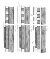
- Figures 3a to 3c illustrate the method according to a further embodiment.
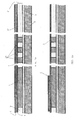
- Figures 4a and 4b illustrate embodiments of a device structure according to the invention.
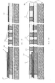
- Figures 5a and 5b illustrate embodiments of a resistor device that can be produced together with a MIMCAP according to the invention.
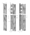
- Figure 1 illustrates one embodiment of the method according to the invention for producing a MIMCAP according to the invention, located between two copper metallization layers produced on a substrate.
- the substrate may for example be an active or passive interposer substrate onto which various integrated circuit chips are to be assembled.
- Figure 1a shows the substrate as a Silicon base substrate 1, provided with an isolation layer 2.
- the isolation layer 2 could be a layer consisting of silicon oxide or silicon nitride or silicon carbide or a combination (e.g. a stack) of two or three of these materials.
- the substrate may be a glass substrate (i.e. instead of the combined Si+isolation layer).
- a first metallization layer M1 is produced by a damascene process as known per se in the art.
- a first layer 3 of inter-metal dielectric (IMD) is deposited, and patterned by a patterning step as defined above, to form openings and/or trenches, which are then lined with a barrier layer for preventing Cu-diffusion into the IMD combined with a copper seed deposited by a suitable deposition technique (such as physical or chemical vapour deposition - PVD or CVD) as known in the art.
- a suitable deposition technique such as physical or chemical vapour deposition - PVD or CVD
- ECD electrochemical deposition
- the first metallization layer M1 thus obtained comprises at least one plate 4 which is to form the bottom plate of the MIMCAP. This may be a rectangular plate for example.
- the bottom plate 4 is preferably provided with perforations (not shown) filled with dielectric, which serve to maintain flatness of the bottom plate during CMP.
- the perforations are obtained as non-etched IMD portions during the IMD patterning step, onto which the copper is deposited, the copper filling the spaces between the IMD portions.
- three further copper structures 5 are shown, for example conductors running along a pre-defined pattern in the first metallization layer M1. Then a stack of three layers is deposited on the planarized surface ( fig. 1c ), for example by a PVD deposition step : a first electrically conductive layer 6, a dielectric layer 7 and a second electrically conductive layer 7.
- these electrically conductive layers 6 and 8 will be referred to as 'conductive layers' for reasons of conciseness. They may be metal layers or layers of materials like TiN or TaN.
- the stack of layers 6/7/8 is patterned, to form the MIM-stack 9 ( fig. 1d ), which covers at least a portion of the bottom plate 4.
- a further IMD layer 10 ( fig. 1e ), which is patterned to form at least one opening 11 on top of the MIM-stack, as well as vias 12 towards some of the structures 5 ( fig. 1f ).
- the openings are filled with copper and planarized, resulting in the second metallization layer M2, comprising the top plate 13 (equally preferably perforated for maintaining flatness), in contact with the second conductive layer 8 of the MIM-stack ( fig. 1g ), as well as via connections 14 for connecting the structures 5 with a further metallization layer.
- the final MIMCAP-structure 50 consists of a portion of the bottom plate 4, first conductive layer 6, dielectric 7, second conductive layer 8 and top plate 13.
- the MIMCAP as such is characterized by the presence of a bottom plate 4, first conductive layer 6 in contact with the bottom plate 4, dielectric layer 7 in contact with the first conductive layer 6, second conductive layer 8 in contact with the dielectric layer 7, and top plate 13 in contact with the second conductive layer, wherein the bottom plate is part of a first metallization layer and the top plate is part of a second metallization layer in a metallization stack coupled between one or more semiconductor devices and an external power source.
- the formation of the MIM-stack 9 takes place by multiple patterning steps, wherein in the first patterning step, the first conductive layer 6 remains intact on the surface of the planarized first metallization layer M1, while the dielectric 7 and the second conductive layer 8 are patterned to form a stack of these two layers covering at least a portion of the bottom plate 4.
- a second patterning step is performed to pattern the first conductive layer 6 and possibly the second conductive layer 8 simultaneously. In this way, the first conductive layer can be used to form additional structures within the first metallization layer M1.
- FIG 2 This embodiment is illustrated in figure 2 .
- Figure 2a shows the stage where the stack of layers 6/7/8 described in relation to figure 1 , has been deposited on the planarized first metallization layer M1.
- the structures 15 are part of an inductor pattern in the first metallization layer M1, while the MIM-stack also extends over a portion 3' of the IMD 3 of M1, with no metal present in said portion.
- Figure 2b shows the result of a first patterning step wherein only the dielectric layer 7 and the second conductive layer 8 are patterned to form a MIM-stack 9 which covers at least a portion of the bottom plate 4.
- the MIM-stack 9 consists of the remainder of the dielectric layer 7 and second conductive layer 8, and of a portion of the first conductive layer 6, said conductive layer being still intact on the whole surface of the first metallization layer M1.
- the etching of layers 7 and 8 stops on the first conductive layer 6 (possible by suitable choice of etchant in relation to the material of the first conductive layer 6).
- the first conductive layer 6 is patterned, as shown in figure 2c . Portions 20 and 21 of said layer 6 to the left and right of the MIM stack remain. Furthermore, a portion 22 above the inductor structure 15 and covering the entire inductor structure remains as well. Finally, a rectangular portion 23 remains on the portion 10' of the IMD. These portions 20 to 23 of the first conductive layer 6 can now serve as additional structural elements in the metallization layout. Deposition and patterning of the second metallization layer M2 results in the view of figure 2d , once again with the top copper plate 24 on and in contact with the second conductive layer 8 of the MIM-stack.
- a via 25 is produced for contacting the first conductive layer 6 and thus the bottom plate 4 from the second metallization layer M2.
- Vias 26 are provided for contacting the inductor 15, while rectangular vias 27, as seen in the top view of figure 2e , are produced for connecting the rectangular portion 23 of the first conductive layer to the second metallization layer M2.
- said rectangular portion 23 may be integrated as a resistor in the circuit defined within said second metallization layer M2.
- the function of the inductor shaped portion 22 of layer 6 and of the portion 21 to the right of the MIMCAP (contacted by via 25) is to provide an advantage in the processing of the M1 and M2 layers : when etching the vias 25 and 26 for example, the etching stops on the first conductive layer 6 (e.g. a TaN layer), and not on the Cu. Stopping on a Cu layer leads to contamination of the etching chamber, which complicates the process.
- the presence of the first conductive layer 6 makes it possible to avoid those complications (by patterning the portion 22) at least during processing of the M1 and M2 layers, which is particularly advantageous given the high copper density of the layers M1 and M2. So even though the invention is not limited (as seen in figure 1 for example) to the embodiment wherein portions of the first conductive layer 6 remain on inductors and/or other structures in the M1 level, the invention does represent a considerable advantage in providing this possibility.
- the patterned portion 22 of layer 6 plays itself the part of an inductor (i.e. without the inductor pattern 15 in the M1 level), although the thickness of the inductor pattern 22 would be insufficient for serving as a workable inductor in many practical circumstances in terms of the material and thickness of the metallization layers and the MIM-stack layers.
- the patterned portions of the first conductive layer 6 may serve as contact portions for structures (such as inductor 15) in one of the metallization layers M1/M2 or said portions may themselves play the part of circuit elements in said metallization layers (such as the resistor 23, or theoretically, the inductor pattern 22).
- the patterning step executed for patterning the first conductive layer 6 serves also to pattern the portion of the second conductive layer 8 that forms the top layer of the MIM stack 9.
- this patterning is to the effect that a ring structure 30 (not necessarily circular-shaped) is formed surrounding a central portion 31 of said top conductive layer 8, in the plane of the MIMCAP.
- the top copper plate 24 then only contacts the central portion 31.
- the ring portion 30 serves to prevent possible shorting between the top and bottom electrodes at the edge of the capacitor.
- the structure of the MIMCAP of the invention, and its production method allow to produce such a protective ring 30 simultaneously with the patterning of the first conductive layer 6, and thus provides an economic way of producing complex structures.
- the first conductive layer 6 remains intact after a first patterning step, as in the embodiments of figures 2 and 3 , but in the second patterning step, it is only the second conductive layer 8 which is further patterned, for example to form a ring structure 30, while the first conductive layer 6 still remains intact.
- This final structure is illustrated in figures 4a and 4b .
- the bottom plate of the MIMCAP is a portion of a larger metal layer in the M1-level.
- the step of patterning the dielectric layer 7 and the second conductive layer 8 of the MIM-stack, with the first conductive layer 6 remaining intact does not only take place at the location of the eventual MIMCAP above the bottom plate 4, but a stack of portions 7' and 8' of these layers 7 and 8 may also remain on other locations.
- an additional stack 40 of these portions 7' and 8' is produced on the resistor portion 23.
- This stack 40 provides a protection of a large portion of the resistor metal during the etching of the dielectric 7 in other areas. This therefore allows a better control of the resistance value of the resistor.
- the stack 40 may be further provided with a connection 28 to the next metallization layer ( figure 5b ).
- the IMD material may be silicon oxide (SiO 2 ) or a combination of SiO 2 with silicon nitride (Si 3 N 4 ) or a combination of SiO 2 with silicon carbide (SiC).
- the IMD may also be a low-k material.
- the thickness of the M1 and M2 levels may be according to known practice in the domain of damascene processing, e.g. around 1micron.
- the thickness of the M2 layer may be chosen higher than M1 given that the CMP step will generally take longer as the topography caused by the MIM-stack patterning needs to be removed.
- the first and second conductive layer 6/8 of the MIM-stack may be for example Ta, TaN, Ti or TiN, but other suitable materials may be applicable.
- the layers 6, 7 and 8 preferably have the same thickness, e.g. between 50nm and 100nm. At least the thickness of the first and second conductive layer 6 and 8 is preferably the same, especially in the embodiment of figure 2 , where both layers are etched in the same etching step.
- the dielectric layer 7 of the MIM-stack may be for example SiO 2 , silicon nitride (Si 3 N 4 ), silicon carbide, Ta 2 O 5 , hafnium oxide, TiO 2 , an ONO-stack (Oxide-nitride-oxide), or any other suitable material.
- an annealing step can be performed prior to the CMP done on the first metallization layer M1.
- the annealing temperature is preferably between 350°C and 450°C.
- the annealing is done to decrease hillocks formation due to stress induced by the subsequent steps (MIM-stack deposition).
- the invention can be integrated in existing BEOL process schemes.
- the MIMCAP of the invention is integrated in an interposer substrate, in particular between the power supply layer the ground layer of such an interposer. This is particularly advantageous due to the large surface that is available for the MIMCAP.
Landscapes
- Semiconductor Integrated Circuits (AREA)
- Internal Circuitry In Semiconductor Integrated Circuit Devices (AREA)
- Engineering & Computer Science (AREA)
- Power Engineering (AREA)
- Physics & Mathematics (AREA)
- Geometry (AREA)
Abstract
Description
- The present invention is related to semiconductor processing. The invention is in particular related to a metal-insulator-metal capacitor and its integration in the back-end-of-line (BEOL) processing of a semiconductor package.
- Device downscaling in present day CMOS technology is leading to faster switching speeds of the transistors integrated with a higher density on the semiconductor wafer. However, in the final device, large current spikes may occur due to a large number of 'simultaneous' switching events in the circuit within a short period of time, which can cause considerable current-resistance drop and noise over the power supply network. Voltage fluctuation and power supply noise may impact signal integrity, speed and reliability of the devices. It has been shown that the addition of an on-chip decoupling MIMCAP (Metal-Insulator-Metal capacitor) can reduce this problem and enhance circuit performance. The MIMCAP can compensate voltage fluctuations by delivering charges to the power-supply network. However, its capacitance needs to be large enough to be actually efficient. In addition, low resistance and low inductance is needed to enable the efficient application of MIMCAPs at high frequencies. In present day MIMCAP designs, resistance especially is too high for this purpose because of the connections from at least one of the metallization levels to the top and/or the bottom plate of the MIMCAP. Such connections are established by via etching and filling techniques, typically increasing the resistance of the path from said metallization layer(s) to the MIMCAP.
- The invention is related to a MIMCAP design that does not suffer from the above-described problem. The invention is in particular related to a MIMCAP structure as disclosed in the appended claims and to a method for producing such a structure. A MIMCAP according to the invention is located between a first and second metallization layer in a stack of metallization layers, in particular copper metallization layers, obtainable by single damascene processing steps as known in the art, said stack supporting semiconductor devices, which are connected through said metallization layers to an external power source. The MIMCAP comprises a bottom plate in the first metallization layer, a first conductive layer on and in electrical contact with said bottom plate, a dielectric layer on and in contact with said first conductive layer, a second conductive layer on and in contact with said dielectric layer, and a top plate in the second metallization layer, on and in electrical contact with the second metal plate. The contacting of the bottom and top plates of the MIMCAP from the first and second metallization layer is thereby established without vias between said plates and said metallization layers. In addition, the first conductive layer of the MIMCAP may extend beyond the surface of the dielectric and the second layer for forming other structures.
- In particular, the invention is related to a semiconductor device package comprising one or more semiconductor devices electrically coupled to a metallization stack, said stack comprising a plurality of interconnected metallization layers, wherein a metal-insulator-metal capacitor is mounted between two of said metallization layers, a lower layer and an upper layer, said layers being directly adjacent in the stack, said capacitor comprising :
- At least a portion of a bottom plate which is part of the lower metallization layer,
- At least a portion of a first conductive layer on and in contact with said bottom plate,
- A dielectric layer on and in contact with said first conductive layer,
- A second conductive layer on and in contact with said dielectric layer,
- A top plate which is part of the upper metallization layer, said top plate being on and in contact with said second conductive layer.
- According to an embodiment, the first and second conductive layer and the dielectric layer in between said layers have the same size in the plane of said layers.
- According to another embodiment, the first conductive layer extends beyond the surface of the dielectric layer and the second dielectric layer.
- In the latter case, said first conductive layer may be patterned in the area outside the area covered by the MIMCAP. Said first conductive layer may be patterned to form one or more patterned portions, which serve as contact portions for electrical circuit elements in the lower or upper metallization layer and/or which serve themselves as said electrical circuit elements.
- According to an embodiment, a patterned portion of the first conductive layer forms a resistor in the upper metallization layer, and wherein a stack of a dielectric layer portion and a top conductive layer portion is present on top of said resistor, said dielectric layer and top conductive layer portion being of the same material and thickness of said dielectric layer and second conductive layer of said capacitor.
- According to an embodiment, the second conductive layer is surrounded in the plane of the layer by a ring structure of the same material and thickness of said second conductive layer.
- Said first and second metallization layer may be the power supply layer and the ground layer respectively of an interposer substrate carrying one or more integrated circuit devices.
- Said bottom and/or top plate may be provided with perforations through the complete thickness of the plates, said perforations being filled with a dielectric material.
- The invention is equally related to a method for producing a semiconductor package according to the invention, comprising the steps of :
- Producing a first metallization layer by a damascene process, said first metallization layer comprising a bottom plate,
- Depositing a stack of a first conductive layer, a dielectric layer and a second conductive layer on and in contact with said first metallization layer,
- Patterning at least the second layer and the dielectric layer to form a stack of the first conductive layer or a portion thereof, the dielectric layer and the second conductive layer, which covers at least partially said bottom plate,
- Producing a second metallization layer by a damascene process, said second metallization layer comprising a top plate which is on and in contact with the second conductive layer of said stack.
- In the method of the invention, said patterning step may be performed to the effect of forming a stack of the first conductive layer, the dielectric layer and the second conductive layer, said layers being of the same size in the plane of said layers.
- According to another embodiment, said patterning step is performed to the effect of forming a stack of the dielectric layer and the second conductive layer on top of the first conductive layer, said first conductive layer remaining intact after said patterning step.
- According to an embodiment, said first conductive layer is further patterned in a second patterning step. During said second patterning step, said first conductive layer and the second conductive layer portion of said stack may be patterned simultaneously.
- During said second patterning step, the second conductive layer portion of the stack may be patterned to form a ring structure around a central portion of the second conductive layer.
-
Figures 1a to 1e illustrate the steps of the method according to one embodiment of the invention. -
Figures 2a to 2e illustrate the method according to a more specific embodiment. -
Figures 3a to 3c illustrate the method according to a further embodiment. -
Figures 4a and 4b illustrate embodiments of a device structure according to the invention. -
Figures 5a and 5b illustrate embodiments of a resistor device that can be produced together with a MIMCAP according to the invention. - Definitions :
- Metallization layer : one of a stack of layers of a dielectric material, with electrically conductive material forming a pattern embedded in said layer. Subsequent metallization layers in the stack are isolated from each other except through vertical connections between the electrically conductive material.
- patterning step : procedure in which portions of a layer are removed by etching away said portions while the remainder of the layer is protected by an etch mask,
- leaving a pattern formed by the remaining parts of the layer. The patterning may take place by known photolithography techniques involving a resist layer, or by hard mask techniques, equally known in the art.
-
Figure 1 illustrates one embodiment of the method according to the invention for producing a MIMCAP according to the invention, located between two copper metallization layers produced on a substrate. The substrate may for example be an active or passive interposer substrate onto which various integrated circuit chips are to be assembled.Figure 1a shows the substrate as aSilicon base substrate 1, provided with anisolation layer 2. Theisolation layer 2 could be a layer consisting of silicon oxide or silicon nitride or silicon carbide or a combination (e.g. a stack) of two or three of these materials. Alternatively, the substrate may be a glass substrate (i.e. instead of the combined Si+isolation layer). - On the substrate, a first metallization layer M1 is produced by a damascene process as known per se in the art. A
first layer 3 of inter-metal dielectric (IMD) is deposited, and patterned by a patterning step as defined above, to form openings and/or trenches, which are then lined with a barrier layer for preventing Cu-diffusion into the IMD combined with a copper seed deposited by a suitable deposition technique (such as physical or chemical vapour deposition - PVD or CVD) as known in the art. After that, copper is plated (using electrochemical deposition ECD) to fill openings and/or trenches. The copper which has been plated not only in the openings and trenches but also on top of the IMD, is planarized by a CMP (Chemical Mechanical Polishing) step, which leads to the result shown infigure 1b . The barrier layer is not shown in this drawing. In the method of the invention, the first metallization layer M1 thus obtained comprises at least oneplate 4 which is to form the bottom plate of the MIMCAP. This may be a rectangular plate for example. Thebottom plate 4 is preferably provided with perforations (not shown) filled with dielectric, which serve to maintain flatness of the bottom plate during CMP. The perforations are obtained as non-etched IMD portions during the IMD patterning step, onto which the copper is deposited, the copper filling the spaces between the IMD portions. - By way of example, three further copper structures 5 are shown, for example conductors running along a pre-defined pattern in the first metallization layer M1. Then a stack of three layers is deposited on the planarized surface (
fig. 1c ), for example by a PVD deposition step : a first electricallyconductive layer 6, adielectric layer 7 and a second electricallyconductive layer 7. In the rest of this description and in the claims, these electricallyconductive layers layers 6/7/8 is patterned, to form the MIM-stack 9 (fig. 1d ), which covers at least a portion of thebottom plate 4. This is followed by the deposition of a further IMD layer 10 (fig. 1e ), which is patterned to form at least oneopening 11 on top of the MIM-stack, as well asvias 12 towards some of the structures 5 (fig. 1f ). By another damascene process, the openings are filled with copper and planarized, resulting in the second metallization layer M2, comprising the top plate 13 (equally preferably perforated for maintaining flatness), in contact with the secondconductive layer 8 of the MIM-stack (fig. 1g ), as well as viaconnections 14 for connecting the structures 5 with a further metallization layer. The final MIMCAP-structure 50 consists of a portion of thebottom plate 4, firstconductive layer 6,dielectric 7, secondconductive layer 8 andtop plate 13. - In the method of the invention, no via connections are produced towards the top or bottom plate of the MIMCAP. The MIMCAP as such is characterized by the presence of a
bottom plate 4, firstconductive layer 6 in contact with thebottom plate 4,dielectric layer 7 in contact with the firstconductive layer 6, secondconductive layer 8 in contact with thedielectric layer 7, andtop plate 13 in contact with the second conductive layer, wherein the bottom plate is part of a first metallization layer and the top plate is part of a second metallization layer in a metallization stack coupled between one or more semiconductor devices and an external power source. - According to a specific embodiment, the formation of the MIM-
stack 9 takes place by multiple patterning steps, wherein in the first patterning step, the firstconductive layer 6 remains intact on the surface of the planarized first metallization layer M1, while thedielectric 7 and the secondconductive layer 8 are patterned to form a stack of these two layers covering at least a portion of thebottom plate 4. After that, a second patterning step is performed to pattern the firstconductive layer 6 and possibly the secondconductive layer 8 simultaneously. In this way, the first conductive layer can be used to form additional structures within the first metallization layer M1. - This embodiment is illustrated in
figure 2 .Figure 2a shows the stage where the stack oflayers 6/7/8 described in relation tofigure 1 , has been deposited on the planarized first metallization layer M1. Thestructures 15 are part of an inductor pattern in the first metallization layer M1, while the MIM-stack also extends over a portion 3' of theIMD 3 of M1, with no metal present in said portion.Figure 2b shows the result of a first patterning step wherein only thedielectric layer 7 and the secondconductive layer 8 are patterned to form a MIM-stack 9 which covers at least a portion of thebottom plate 4. The MIM-stack 9 consists of the remainder of thedielectric layer 7 and secondconductive layer 8, and of a portion of the firstconductive layer 6, said conductive layer being still intact on the whole surface of the first metallization layer M1. The etching oflayers - In a second patterning step, the first
conductive layer 6 is patterned, as shown infigure 2c .Portions layer 6 to the left and right of the MIM stack remain. Furthermore, aportion 22 above theinductor structure 15 and covering the entire inductor structure remains as well. Finally, arectangular portion 23 remains on the portion 10' of the IMD. Theseportions 20 to 23 of the firstconductive layer 6 can now serve as additional structural elements in the metallization layout. Deposition and patterning of the second metallization layer M2 results in the view offigure 2d , once again with thetop copper plate 24 on and in contact with the secondconductive layer 8 of the MIM-stack. A via 25 is produced for contacting the firstconductive layer 6 and thus thebottom plate 4 from the second metallization layer M2.Vias 26 are provided for contacting theinductor 15, whilerectangular vias 27, as seen in the top view offigure 2e , are produced for connecting therectangular portion 23 of the first conductive layer to the second metallization layer M2. In this way, saidrectangular portion 23 may be integrated as a resistor in the circuit defined within said second metallization layer M2. - The function of the inductor shaped
portion 22 oflayer 6 and of theportion 21 to the right of the MIMCAP (contacted by via 25) is to provide an advantage in the processing of the M1 and M2 layers : when etching thevias conductive layer 6 makes it possible to avoid those complications (by patterning the portion 22) at least during processing of the M1 and M2 layers, which is particularly advantageous given the high copper density of the layers M1 and M2. So even though the invention is not limited (as seen infigure 1 for example) to the embodiment wherein portions of the firstconductive layer 6 remain on inductors and/or other structures in the M1 level, the invention does represent a considerable advantage in providing this possibility. - In the case of the
inductor 15, it is not excluded that the patternedportion 22 oflayer 6 plays itself the part of an inductor (i.e. without theinductor pattern 15 in the M1 level), although the thickness of theinductor pattern 22 would be insufficient for serving as a workable inductor in many practical circumstances in terms of the material and thickness of the metallization layers and the MIM-stack layers. In general, it can be said that the patterned portions of the firstconductive layer 6 may serve as contact portions for structures (such as inductor 15) in one of the metallization layers M1/M2 or said portions may themselves play the part of circuit elements in said metallization layers (such as theresistor 23, or theoretically, the inductor pattern 22). - In a still further embodiment, the patterning step executed for patterning the first
conductive layer 6 serves also to pattern the portion of the secondconductive layer 8 that forms the top layer of theMIM stack 9. According to a preferred embodiment illustrated infigure 3 , this patterning is to the effect that a ring structure 30 (not necessarily circular-shaped) is formed surrounding acentral portion 31 of said topconductive layer 8, in the plane of the MIMCAP. Thetop copper plate 24 then only contacts thecentral portion 31. Thering portion 30 serves to prevent possible shorting between the top and bottom electrodes at the edge of the capacitor. The structure of the MIMCAP of the invention, and its production method allow to produce such aprotective ring 30 simultaneously with the patterning of the firstconductive layer 6, and thus provides an economic way of producing complex structures. - According to another embodiment, the first
conductive layer 6 remains intact after a first patterning step, as in the embodiments offigures 2 and3 , but in the second patterning step, it is only the secondconductive layer 8 which is further patterned, for example to form aring structure 30, while the firstconductive layer 6 still remains intact. This final structure is illustrated infigures 4a and 4b . In these embodiments, there is no separate step of processing a separate bottom plate having dimensions that are in the same order of magnitude as thetop plate - According to an embodiment, the step of patterning the
dielectric layer 7 and the secondconductive layer 8 of the MIM-stack, with the firstconductive layer 6 remaining intact, does not only take place at the location of the eventual MIMCAP above thebottom plate 4, but a stack of portions 7' and 8' of theselayers figure 5a and 5b , anadditional stack 40 of these portions 7' and 8' is produced on theresistor portion 23. Thisstack 40 provides a protection of a large portion of the resistor metal during the etching of the dielectric 7 in other areas. This therefore allows a better control of the resistance value of the resistor. Thestack 40 may be further provided with aconnection 28 to the next metallization layer (figure 5b ). - The IMD material may be silicon oxide (SiO2) or a combination of SiO2 with silicon nitride (Si3N4) or a combination of SiO2 with silicon carbide (SiC). The IMD may also be a low-k material. The metallization metal used in preferably copper. The thickness of the M1 and M2 levels may be according to known practice in the domain of damascene processing, e.g. around 1micron. The thickness of the M2 layer may be chosen higher than M1 given that the CMP step will generally take longer as the topography caused by the MIM-stack patterning needs to be removed.
- The first and second
conductive layer 6/8 of the MIM-stack may be for example Ta, TaN, Ti or TiN, but other suitable materials may be applicable. Thelayers conductive layer figure 2 , where both layers are etched in the same etching step. - The
dielectric layer 7 of the MIM-stack may be for example SiO2, silicon nitride (Si3N4), silicon carbide, Ta2O5, hafnium oxide, TiO2, an ONO-stack (Oxide-nitride-oxide), or any other suitable material. - According to an embodiment, an annealing step can be performed prior to the CMP done on the first metallization layer M1. The annealing temperature is preferably between 350°C and 450°C. The annealing is done to decrease hillocks formation due to stress induced by the subsequent steps (MIM-stack deposition).
- The invention can be integrated in existing BEOL process schemes. According to a preferred embodiment, the MIMCAP of the invention is integrated in an interposer substrate, in particular between the power supply layer the ground layer of such an interposer. This is particularly advantageous due to the large surface that is available for the MIMCAP.
- While the invention has been illustrated and described in detail in the drawings and foregoing description, such illustration and description are to be considered illustrative or exemplary and not restrictive. Other variations to the disclosed embodiments can be understood and effected by those skilled in the art in practicing the claimed invention, from a study of the drawings, the disclosure and the appended claims. In the claims, the word "comprising" does not exclude other elements or steps, and the indefinite article "a" or "an" does not exclude a plurality. The mere fact that certain measures are recited in mutually different dependent claims does not indicate that a combination of these measures cannot be used to advantage. Any reference signs in the claims should not be construed as limiting the scope.
- The foregoing description details certain embodiments of the invention. It will be appreciated, however, that no matter how detailed the foregoing appears in text, the invention may be practiced in many ways, and is therefore not limited to the embodiments disclosed. It should be noted that the use of particular terminology when describing certain features or aspects of the invention should not be taken to imply that the terminology is being re-defined herein to be restricted to include any specific characteristics of the features or aspects of the invention with which that terminology is associated.
- Unless specifically specified, the description of a layer being deposited or produced 'on' another layer or substrate, includes the options of
- said layer being produced or deposited directly on, i.e. in contact with, said other layer or substrate, and
- said layer being produced on one or a stack of intermediate layers between said layer and said other layer or substrate.
Claims (15)
- A semiconductor device package comprising one or more semiconductor devices electrically coupled to a metallization stack, said stack comprising a plurality of interconnected metallization layers, wherein a metal-insulator-metal capacitor (50) is mounted between two of said metallization layers, a lower layer (M1) and an upper layer (M2), said layers being directly adjacent in the stack, said capacitor comprising :• At least a portion of a bottom plate (4) which is part of the lower metallization layer (M1),• At least a portion of a first conductive layer (6) on and in contact with said bottom plate,• A dielectric layer (7) on and in contact with said first conductive layer,• A second conductive layer (8,31) on and in contact with said dielectric layer,• A top plate (13,24) which is part of the upper metallization layer, said top plate being on and in contact with said second conductive layer (8).
- Semiconductor package according to claim 1, wherein the first and second conductive layer (6,8) and the dielectric layer (7) in between said layers have the same size in the plane of said layers.
- Semiconductor package according to claim 1, wherein the first conductive layer (6) extends beyond the surface of the dielectric layer (7) and the second dielectric layer (8).
- Semiconductor package according to claim 3, wherein said first conductive layer (6) is patterned in the area outside the area covered by the MIMCAP (50).
- Semiconductor package according to claim 3, wherein said first conductive layer (6) is patterned to form one or more patterned portions (22,23), which serve as contact portions for electrical circuit elements (15) in the lower or upper metallization layer (M1,M2) and/or which serve themselves as said electrical circuit elements.
- Semiconductor package according to claim 5, wherein a patterned portion (23) of the first conductive layer (6) forms a resistor in the upper metallization layer (M2), and wherein a stack of a dielectric layer portion (7') and a top conductive layer portion (8') is present on top of said resistor, said dielectric layer (7') and top conductive layer portion (8') being of the same material and thickness of said dielectric layer (7) and second conductive layer (8) of said capacitor (50).
- Semiconductor package according to any one of claims 3 to 6, wherein the second conductive layer (31) is surrounded in the plane of the layer by a ring structure (30) of the same material and thickness of said second conductive layer (31).
- Semiconductor package according to any one of claims 1 to 7, wherein said first and second metallization layer (M1, M2) are the power supply layer and the ground layer respectively of an interposer substrate carrying one or more integrated circuit devices.
- Semiconductor package according to any one of claims 1 to 8, wherein said bottom and/or top plate are provided with perforations through the complete thickness of the plates, said perforations being filled with a dielectric material.
- A method for producing a semiconductor package according to any one of claims 1 to 9, comprising the steps of :• Producing a first metallization layer (M1) by a damascene process, said first metallization layer comprising a bottom plate (4),• Depositing a stack of a first conductive layer (6), a dielectric layer (7) and a second conductive layer (8) on and in contact with said first metallization layer (M1),• Patterning at least the second layer (8) and the dielectric layer (7) to form a stack (9) of the first conductive layer (6) or a portion thereof, the dielectric layer (7) and the second conductive layer (8), which covers at least partially said bottom plate (4),• Producing a second metallization layer (M2) by a damascene process, said second metallization layer comprising a top plate (13,24) which is on and in contact with the second conductive layer (8) of said stack (9).
- Method according to claim 10, wherein said patterning step is performed to the effect of forming a stack of the first conductive layer (6), the dielectric layer (7) and the second conductive layer (8), said layers being of the same size in the plane of said layers.
- Method according to claim 10, wherein said patterning step is performed to the effect of forming a stack of the dielectric layer (7) and the second conductive layer (8) on top of the first conductive layer, said first conductive layer (6) remaining intact after said patterning step.
- Method according to claim 12, wherein said first conductive layer (6) is further patterned in a second patterning step.
- Method according to claim 11 or 12, wherein during said second patterning step, said first conductive layer (6) and the second conductive layer portion (8) of said stack (9) are patterned simultaneously.
- Method according to claim 12, wherein during said second patterning step, the second conductive layer portion (8) of the stack (9) is patterned to form a ring structure (30) around a central portion (31) of the second conductive layer.
Priority Applications (4)
| Application Number | Priority Date | Filing Date | Title |
|---|---|---|---|
| EP12194922.6A EP2738827B1 (en) | 2012-11-29 | 2012-11-29 | MIMCAP structure in a semiconductor device package |
| US14/092,762 US20140151848A1 (en) | 2012-11-29 | 2013-11-27 | Mimcap structure in a semiconductor device package |
| US15/014,343 US20160155699A1 (en) | 2012-11-29 | 2016-02-03 | Mimcap structure in a semiconductor device package |
| US15/411,891 US10256183B2 (en) | 2012-11-29 | 2017-01-20 | MIMCAP structure in a semiconductor device package |
Applications Claiming Priority (1)
| Application Number | Priority Date | Filing Date | Title |
|---|---|---|---|
| EP12194922.6A EP2738827B1 (en) | 2012-11-29 | 2012-11-29 | MIMCAP structure in a semiconductor device package |
Publications (2)
| Publication Number | Publication Date |
|---|---|
| EP2738827A1 true EP2738827A1 (en) | 2014-06-04 |
| EP2738827B1 EP2738827B1 (en) | 2022-04-06 |
Family
ID=47325894
Family Applications (1)
| Application Number | Title | Priority Date | Filing Date |
|---|---|---|---|
| EP12194922.6A Active EP2738827B1 (en) | 2012-11-29 | 2012-11-29 | MIMCAP structure in a semiconductor device package |
Country Status (2)
| Country | Link |
|---|---|
| US (3) | US20140151848A1 (en) |
| EP (1) | EP2738827B1 (en) |
Families Citing this family (4)
| Publication number | Priority date | Publication date | Assignee | Title |
|---|---|---|---|---|
| US20160293334A1 (en) * | 2015-03-31 | 2016-10-06 | Tdk Corporation | Thin film capacitor |
| US10714420B1 (en) | 2019-01-02 | 2020-07-14 | International Business Machines Corporation | High cutoff frequency metal-insulator-metal capacitors implemented using via contact configurations |
| CN112259521B (en) * | 2020-10-20 | 2022-08-16 | 华虹半导体(无锡)有限公司 | MIM capacitor for improving contact stress of electrode plate |
| TWI824677B (en) * | 2022-08-25 | 2023-12-01 | 同欣電子工業股份有限公司 | Chip packaging structure and method for fabricating the same |
Citations (5)
| Publication number | Priority date | Publication date | Assignee | Title |
|---|---|---|---|---|
| US20030211731A1 (en) * | 2002-05-07 | 2003-11-13 | Chartered Semiconductor Manufacturing Ltd. | Metal sandwich structure for MIM capacitor onto dual damascene |
| US20040106266A1 (en) * | 2002-12-02 | 2004-06-03 | Taiwan Semiconductor Manufacturing Company | Novel method to fabricate high reliable metal capacitor within copper back-end process |
| US20050095781A1 (en) * | 2003-10-30 | 2005-05-05 | Papa Rao Satyavolu S. | Capacitor integration at top-metal level with a protection layer for the copper surface |
| US20050098815A1 (en) * | 2002-04-16 | 2005-05-12 | Fujitsu Limited | Laser having active region formed above substrate |
| US20110062549A1 (en) * | 2009-09-11 | 2011-03-17 | Stats Chippac, Ltd. | Semiconductor Device and Method of Forming Integrated Passive Device |
Family Cites Families (11)
| Publication number | Priority date | Publication date | Assignee | Title |
|---|---|---|---|---|
| US5583359A (en) * | 1995-03-03 | 1996-12-10 | Northern Telecom Limited | Capacitor structure for an integrated circuit |
| US5831331A (en) * | 1996-11-22 | 1998-11-03 | Philips Electronics North America Corporation | Self-shielding inductor for multi-layer semiconductor integrated circuits |
| US6395996B1 (en) * | 2000-05-16 | 2002-05-28 | Silicon Integrated Systems Corporation | Multi-layered substrate with a built-in capacitor design |
| US6737728B1 (en) * | 2000-10-12 | 2004-05-18 | Intel Corporation | On-chip decoupling capacitor and method of making same |
| US6791133B2 (en) * | 2002-07-19 | 2004-09-14 | International Business Machines Corporation | Interposer capacitor built on silicon wafer and joined to a ceramic substrate |
| US7112507B2 (en) * | 2003-11-24 | 2006-09-26 | Infineon Technologies Ag | MIM capacitor structure and method of fabrication |
| US7049170B2 (en) * | 2003-12-17 | 2006-05-23 | Tru-Si Technologies, Inc. | Integrated circuits and packaging substrates with cavities, and attachment methods including insertion of protruding contact pads into cavities |
| US20080113455A1 (en) * | 2006-11-11 | 2008-05-15 | Rajesh Jain | Planar etching of dissimilar materials |
| US7759212B2 (en) * | 2007-12-26 | 2010-07-20 | Stats Chippac, Ltd. | System-in-package having integrated passive devices and method therefor |
| US7863724B2 (en) * | 2008-02-12 | 2011-01-04 | International Business Machines Corporation | Circuit substrate having post-fed die side power supply connections |
| US7791897B2 (en) * | 2008-09-09 | 2010-09-07 | Endicott Interconnect Technologies, Inc. | Multi-layer embedded capacitance and resistance substrate core |
-
2012
- 2012-11-29 EP EP12194922.6A patent/EP2738827B1/en active Active
-
2013
- 2013-11-27 US US14/092,762 patent/US20140151848A1/en not_active Abandoned
-
2016
- 2016-02-03 US US15/014,343 patent/US20160155699A1/en not_active Abandoned
-
2017
- 2017-01-20 US US15/411,891 patent/US10256183B2/en active Active
Patent Citations (5)
| Publication number | Priority date | Publication date | Assignee | Title |
|---|---|---|---|---|
| US20050098815A1 (en) * | 2002-04-16 | 2005-05-12 | Fujitsu Limited | Laser having active region formed above substrate |
| US20030211731A1 (en) * | 2002-05-07 | 2003-11-13 | Chartered Semiconductor Manufacturing Ltd. | Metal sandwich structure for MIM capacitor onto dual damascene |
| US20040106266A1 (en) * | 2002-12-02 | 2004-06-03 | Taiwan Semiconductor Manufacturing Company | Novel method to fabricate high reliable metal capacitor within copper back-end process |
| US20050095781A1 (en) * | 2003-10-30 | 2005-05-05 | Papa Rao Satyavolu S. | Capacitor integration at top-metal level with a protection layer for the copper surface |
| US20110062549A1 (en) * | 2009-09-11 | 2011-03-17 | Stats Chippac, Ltd. | Semiconductor Device and Method of Forming Integrated Passive Device |
Also Published As
| Publication number | Publication date |
|---|---|
| US10256183B2 (en) | 2019-04-09 |
| US20160155699A1 (en) | 2016-06-02 |
| EP2738827B1 (en) | 2022-04-06 |
| US20140151848A1 (en) | 2014-06-05 |
| US20170194246A1 (en) | 2017-07-06 |
Similar Documents
| Publication | Publication Date | Title |
|---|---|---|
| CN108461477B (en) | Metal Interconnects for Ultra (Jump) Via Integration | |
| EP3174094B1 (en) | Integrated circuit comprising a metal-insulator-metal capacitor and fabrication method thereof | |
| CN106170858B (en) | capacitor structure | |
| KR100773256B1 (en) | Stacked structure for parallel capacitors and method of fabrication | |
| US20100178747A1 (en) | Minimum Cost Method for Forming High Density Passive Capacitors for Replacement of Discrete Board Capacitors Using a Minimum Cost 3D Wafer-to-Wafer Modular Integration Scheme | |
| CN110060982B (en) | Capacitor for interposer and method of making the same | |
| US9831171B2 (en) | Capacitors with barrier dielectric layers, and methods of formation thereof | |
| JP2009099991A (en) | Stack capacitor of semiconductor device and method of forming the same | |
| US7586142B2 (en) | Semiconductor device having metal-insulator-metal capacitor and method of fabricating the same | |
| US20210265263A1 (en) | Metal-insulator-metal (mim) capacitor | |
| KR100889556B1 (en) | Inductor of semiconductor device and manufacturing method thereof | |
| US10256183B2 (en) | MIMCAP structure in a semiconductor device package | |
| JP3566658B2 (en) | Capacitor and method of forming the same | |
| US10504821B2 (en) | Through-silicon via structure | |
| US20050140010A1 (en) | Method and structure of manufacturing high capacitance metal on insulator capacitors in copper | |
| US20250210401A1 (en) | Method for forming semiconductor structure | |
| US9484398B2 (en) | Metal-insulator-metal (MIM) capacitor | |
| US10734444B1 (en) | Integrated circuits with integrated memory structures and capacitors and methods for fabricating the same | |
| JP4211910B2 (en) | Manufacturing method of semiconductor device | |
| US20120241972A1 (en) | Layout scheme for an input output cell | |
| US20050086780A1 (en) | Method of fabricating circular or angular spiral MIM capacitors | |
| JP4376030B2 (en) | Manufacturing method of semiconductor device provided with MIM capacitance element | |
| KR100800823B1 (en) | Method for manufacturing wiring of semiconductor device having MIM capacitor | |
| KR100922558B1 (en) | Metal wiring of semiconductor device and manufacturing method thereof | |
| US7743482B2 (en) | Fabricating method of a semiconductor device |
Legal Events
| Date | Code | Title | Description |
|---|---|---|---|
| PUAI | Public reference made under article 153(3) epc to a published international application that has entered the european phase |
Free format text: ORIGINAL CODE: 0009012 |
|
| 17P | Request for examination filed |
Effective date: 20121129 |
|
| AK | Designated contracting states |
Kind code of ref document: A1 Designated state(s): AL AT BE BG CH CY CZ DE DK EE ES FI FR GB GR HR HU IE IS IT LI LT LU LV MC MK MT NL NO PL PT RO RS SE SI SK SM TR |
|
| AX | Request for extension of the european patent |
Extension state: BA ME |
|
| R17P | Request for examination filed (corrected) |
Effective date: 20141118 |
|
| RBV | Designated contracting states (corrected) |
Designated state(s): AL AT BE BG CH CY CZ DE DK EE ES FI FR GB GR HR HU IE IS IT LI LT LU LV MC MK MT NL NO PL PT RO RS SE SI SK SM TR |
|
| RAP1 | Party data changed (applicant data changed or rights of an application transferred) |
Owner name: IMEC VZW |
|
| STAA | Information on the status of an ep patent application or granted ep patent |
Free format text: STATUS: EXAMINATION IS IN PROGRESS |
|
| 17Q | First examination report despatched |
Effective date: 20190416 |
|
| GRAP | Despatch of communication of intention to grant a patent |
Free format text: ORIGINAL CODE: EPIDOSNIGR1 |
|
| STAA | Information on the status of an ep patent application or granted ep patent |
Free format text: STATUS: GRANT OF PATENT IS INTENDED |
|
| RIC1 | Information provided on ipc code assigned before grant |
Ipc: H01L 27/01 20060101ALN20211018BHEP Ipc: H01L 23/00 20060101ALI20211018BHEP Ipc: H01L 23/64 20060101ALI20211018BHEP Ipc: H01L 23/522 20060101ALI20211018BHEP Ipc: H01L 49/02 20060101AFI20211018BHEP |
|
| RIC1 | Information provided on ipc code assigned before grant |
Ipc: H01L 27/01 20060101ALN20211025BHEP Ipc: H01L 23/00 20060101ALI20211025BHEP Ipc: H01L 23/64 20060101ALI20211025BHEP Ipc: H01L 23/522 20060101ALI20211025BHEP Ipc: H01L 49/02 20060101AFI20211025BHEP |
|
| RIN1 | Information on inventor provided before grant (corrected) |
Inventor name: BEYNE, ERIC Inventor name: DETALLE, MIKAEL |
|
| INTG | Intention to grant announced |
Effective date: 20211109 |
|
| GRAS | Grant fee paid |
Free format text: ORIGINAL CODE: EPIDOSNIGR3 |
|
| GRAA | (expected) grant |
Free format text: ORIGINAL CODE: 0009210 |
|
| STAA | Information on the status of an ep patent application or granted ep patent |
Free format text: STATUS: THE PATENT HAS BEEN GRANTED |
|
| AK | Designated contracting states |
Kind code of ref document: B1 Designated state(s): AL AT BE BG CH CY CZ DE DK EE ES FI FR GB GR HR HU IE IS IT LI LT LU LV MC MK MT NL NO PL PT RO RS SE SI SK SM TR |
|
| REG | Reference to a national code |
Ref country code: GB Ref legal event code: FG4D |
|
| REG | Reference to a national code |
Ref country code: CH Ref legal event code: EP |
|
| REG | Reference to a national code |
Ref country code: AT Ref legal event code: REF Ref document number: 1482229 Country of ref document: AT Kind code of ref document: T Effective date: 20220415 |
|
| REG | Reference to a national code |
Ref country code: IE Ref legal event code: FG4D |
|
| REG | Reference to a national code |
Ref country code: DE Ref legal event code: R096 Ref document number: 602012077971 Country of ref document: DE |
|
| REG | Reference to a national code |
Ref country code: LT Ref legal event code: MG9D |
|
| REG | Reference to a national code |
Ref country code: NL Ref legal event code: MP Effective date: 20220406 |
|
| REG | Reference to a national code |
Ref country code: AT Ref legal event code: MK05 Ref document number: 1482229 Country of ref document: AT Kind code of ref document: T Effective date: 20220406 |
|
| PG25 | Lapsed in a contracting state [announced via postgrant information from national office to epo] |
Ref country code: NL Free format text: LAPSE BECAUSE OF FAILURE TO SUBMIT A TRANSLATION OF THE DESCRIPTION OR TO PAY THE FEE WITHIN THE PRESCRIBED TIME-LIMIT Effective date: 20220406 |
|
| PG25 | Lapsed in a contracting state [announced via postgrant information from national office to epo] |
Ref country code: SE Free format text: LAPSE BECAUSE OF FAILURE TO SUBMIT A TRANSLATION OF THE DESCRIPTION OR TO PAY THE FEE WITHIN THE PRESCRIBED TIME-LIMIT Effective date: 20220406 Ref country code: PT Free format text: LAPSE BECAUSE OF FAILURE TO SUBMIT A TRANSLATION OF THE DESCRIPTION OR TO PAY THE FEE WITHIN THE PRESCRIBED TIME-LIMIT Effective date: 20220808 Ref country code: NO Free format text: LAPSE BECAUSE OF FAILURE TO SUBMIT A TRANSLATION OF THE DESCRIPTION OR TO PAY THE FEE WITHIN THE PRESCRIBED TIME-LIMIT Effective date: 20220706 Ref country code: LT Free format text: LAPSE BECAUSE OF FAILURE TO SUBMIT A TRANSLATION OF THE DESCRIPTION OR TO PAY THE FEE WITHIN THE PRESCRIBED TIME-LIMIT Effective date: 20220406 Ref country code: HR Free format text: LAPSE BECAUSE OF FAILURE TO SUBMIT A TRANSLATION OF THE DESCRIPTION OR TO PAY THE FEE WITHIN THE PRESCRIBED TIME-LIMIT Effective date: 20220406 Ref country code: GR Free format text: LAPSE BECAUSE OF FAILURE TO SUBMIT A TRANSLATION OF THE DESCRIPTION OR TO PAY THE FEE WITHIN THE PRESCRIBED TIME-LIMIT Effective date: 20220707 Ref country code: FI Free format text: LAPSE BECAUSE OF FAILURE TO SUBMIT A TRANSLATION OF THE DESCRIPTION OR TO PAY THE FEE WITHIN THE PRESCRIBED TIME-LIMIT Effective date: 20220406 Ref country code: ES Free format text: LAPSE BECAUSE OF FAILURE TO SUBMIT A TRANSLATION OF THE DESCRIPTION OR TO PAY THE FEE WITHIN THE PRESCRIBED TIME-LIMIT Effective date: 20220406 Ref country code: BG Free format text: LAPSE BECAUSE OF FAILURE TO SUBMIT A TRANSLATION OF THE DESCRIPTION OR TO PAY THE FEE WITHIN THE PRESCRIBED TIME-LIMIT Effective date: 20220706 Ref country code: AT Free format text: LAPSE BECAUSE OF FAILURE TO SUBMIT A TRANSLATION OF THE DESCRIPTION OR TO PAY THE FEE WITHIN THE PRESCRIBED TIME-LIMIT Effective date: 20220406 |
|
| REG | Reference to a national code |
Ref country code: DE Ref legal event code: R079 Ref document number: 602012077971 Country of ref document: DE Free format text: PREVIOUS MAIN CLASS: H01L0049020000 Ipc: H10N0097000000 |
|
| PG25 | Lapsed in a contracting state [announced via postgrant information from national office to epo] |
Ref country code: RS Free format text: LAPSE BECAUSE OF FAILURE TO SUBMIT A TRANSLATION OF THE DESCRIPTION OR TO PAY THE FEE WITHIN THE PRESCRIBED TIME-LIMIT Effective date: 20220406 Ref country code: PL Free format text: LAPSE BECAUSE OF FAILURE TO SUBMIT A TRANSLATION OF THE DESCRIPTION OR TO PAY THE FEE WITHIN THE PRESCRIBED TIME-LIMIT Effective date: 20220406 Ref country code: LV Free format text: LAPSE BECAUSE OF FAILURE TO SUBMIT A TRANSLATION OF THE DESCRIPTION OR TO PAY THE FEE WITHIN THE PRESCRIBED TIME-LIMIT Effective date: 20220406 Ref country code: IS Free format text: LAPSE BECAUSE OF FAILURE TO SUBMIT A TRANSLATION OF THE DESCRIPTION OR TO PAY THE FEE WITHIN THE PRESCRIBED TIME-LIMIT Effective date: 20220806 |
|
| REG | Reference to a national code |
Ref country code: DE Ref legal event code: R097 Ref document number: 602012077971 Country of ref document: DE |
|
| PG25 | Lapsed in a contracting state [announced via postgrant information from national office to epo] |
Ref country code: SM Free format text: LAPSE BECAUSE OF FAILURE TO SUBMIT A TRANSLATION OF THE DESCRIPTION OR TO PAY THE FEE WITHIN THE PRESCRIBED TIME-LIMIT Effective date: 20220406 Ref country code: SK Free format text: LAPSE BECAUSE OF FAILURE TO SUBMIT A TRANSLATION OF THE DESCRIPTION OR TO PAY THE FEE WITHIN THE PRESCRIBED TIME-LIMIT Effective date: 20220406 Ref country code: RO Free format text: LAPSE BECAUSE OF FAILURE TO SUBMIT A TRANSLATION OF THE DESCRIPTION OR TO PAY THE FEE WITHIN THE PRESCRIBED TIME-LIMIT Effective date: 20220406 Ref country code: EE Free format text: LAPSE BECAUSE OF FAILURE TO SUBMIT A TRANSLATION OF THE DESCRIPTION OR TO PAY THE FEE WITHIN THE PRESCRIBED TIME-LIMIT Effective date: 20220406 Ref country code: DK Free format text: LAPSE BECAUSE OF FAILURE TO SUBMIT A TRANSLATION OF THE DESCRIPTION OR TO PAY THE FEE WITHIN THE PRESCRIBED TIME-LIMIT Effective date: 20220406 Ref country code: CZ Free format text: LAPSE BECAUSE OF FAILURE TO SUBMIT A TRANSLATION OF THE DESCRIPTION OR TO PAY THE FEE WITHIN THE PRESCRIBED TIME-LIMIT Effective date: 20220406 |
|
| PLBE | No opposition filed within time limit |
Free format text: ORIGINAL CODE: 0009261 |
|
| STAA | Information on the status of an ep patent application or granted ep patent |
Free format text: STATUS: NO OPPOSITION FILED WITHIN TIME LIMIT |
|
| 26N | No opposition filed |
Effective date: 20230110 |
|
| PG25 | Lapsed in a contracting state [announced via postgrant information from national office to epo] |
Ref country code: AL Free format text: LAPSE BECAUSE OF FAILURE TO SUBMIT A TRANSLATION OF THE DESCRIPTION OR TO PAY THE FEE WITHIN THE PRESCRIBED TIME-LIMIT Effective date: 20220406 |
|
| PG25 | Lapsed in a contracting state [announced via postgrant information from national office to epo] |
Ref country code: SI Free format text: LAPSE BECAUSE OF FAILURE TO SUBMIT A TRANSLATION OF THE DESCRIPTION OR TO PAY THE FEE WITHIN THE PRESCRIBED TIME-LIMIT Effective date: 20220406 |
|
| P01 | Opt-out of the competence of the unified patent court (upc) registered |
Effective date: 20230513 |
|
| PG25 | Lapsed in a contracting state [announced via postgrant information from national office to epo] |
Ref country code: MC Free format text: LAPSE BECAUSE OF FAILURE TO SUBMIT A TRANSLATION OF THE DESCRIPTION OR TO PAY THE FEE WITHIN THE PRESCRIBED TIME-LIMIT Effective date: 20220406 |
|
| REG | Reference to a national code |
Ref country code: CH Ref legal event code: PL |
|
| GBPC | Gb: european patent ceased through non-payment of renewal fee |
Effective date: 20221129 |
|
| REG | Reference to a national code |
Ref country code: BE Ref legal event code: MM Effective date: 20221130 |
|
| PG25 | Lapsed in a contracting state [announced via postgrant information from national office to epo] |
Ref country code: LI Free format text: LAPSE BECAUSE OF NON-PAYMENT OF DUE FEES Effective date: 20221130 Ref country code: CH Free format text: LAPSE BECAUSE OF NON-PAYMENT OF DUE FEES Effective date: 20221130 |
|
| PG25 | Lapsed in a contracting state [announced via postgrant information from national office to epo] |
Ref country code: LU Free format text: LAPSE BECAUSE OF NON-PAYMENT OF DUE FEES Effective date: 20221129 |
|
| PG25 | Lapsed in a contracting state [announced via postgrant information from national office to epo] |
Ref country code: IE Free format text: LAPSE BECAUSE OF NON-PAYMENT OF DUE FEES Effective date: 20221129 Ref country code: GB Free format text: LAPSE BECAUSE OF NON-PAYMENT OF DUE FEES Effective date: 20221129 |
|
| PG25 | Lapsed in a contracting state [announced via postgrant information from national office to epo] |
Ref country code: FR Free format text: LAPSE BECAUSE OF NON-PAYMENT OF DUE FEES Effective date: 20221130 Ref country code: BE Free format text: LAPSE BECAUSE OF NON-PAYMENT OF DUE FEES Effective date: 20221130 |
|
| PG25 | Lapsed in a contracting state [announced via postgrant information from national office to epo] |
Ref country code: IT Free format text: LAPSE BECAUSE OF FAILURE TO SUBMIT A TRANSLATION OF THE DESCRIPTION OR TO PAY THE FEE WITHIN THE PRESCRIBED TIME-LIMIT Effective date: 20220406 |
|
| PG25 | Lapsed in a contracting state [announced via postgrant information from national office to epo] |
Ref country code: HU Free format text: LAPSE BECAUSE OF FAILURE TO SUBMIT A TRANSLATION OF THE DESCRIPTION OR TO PAY THE FEE WITHIN THE PRESCRIBED TIME-LIMIT; INVALID AB INITIO Effective date: 20121129 |
|
| PG25 | Lapsed in a contracting state [announced via postgrant information from national office to epo] |
Ref country code: CY Free format text: LAPSE BECAUSE OF FAILURE TO SUBMIT A TRANSLATION OF THE DESCRIPTION OR TO PAY THE FEE WITHIN THE PRESCRIBED TIME-LIMIT Effective date: 20220406 |
|
| PG25 | Lapsed in a contracting state [announced via postgrant information from national office to epo] |
Ref country code: MK Free format text: LAPSE BECAUSE OF FAILURE TO SUBMIT A TRANSLATION OF THE DESCRIPTION OR TO PAY THE FEE WITHIN THE PRESCRIBED TIME-LIMIT Effective date: 20220406 |
|
| PG25 | Lapsed in a contracting state [announced via postgrant information from national office to epo] |
Ref country code: TR Free format text: LAPSE BECAUSE OF FAILURE TO SUBMIT A TRANSLATION OF THE DESCRIPTION OR TO PAY THE FEE WITHIN THE PRESCRIBED TIME-LIMIT Effective date: 20220406 |
|
| PG25 | Lapsed in a contracting state [announced via postgrant information from national office to epo] |
Ref country code: MT Free format text: LAPSE BECAUSE OF FAILURE TO SUBMIT A TRANSLATION OF THE DESCRIPTION OR TO PAY THE FEE WITHIN THE PRESCRIBED TIME-LIMIT Effective date: 20220406 |
|
| PG25 | Lapsed in a contracting state [announced via postgrant information from national office to epo] |
Ref country code: BG Free format text: LAPSE BECAUSE OF FAILURE TO SUBMIT A TRANSLATION OF THE DESCRIPTION OR TO PAY THE FEE WITHIN THE PRESCRIBED TIME-LIMIT Effective date: 20220406 |
|
| PG25 | Lapsed in a contracting state [announced via postgrant information from national office to epo] |
Ref country code: BG Free format text: LAPSE BECAUSE OF FAILURE TO SUBMIT A TRANSLATION OF THE DESCRIPTION OR TO PAY THE FEE WITHIN THE PRESCRIBED TIME-LIMIT Effective date: 20220406 |
|
| PGFP | Annual fee paid to national office [announced via postgrant information from national office to epo] |
Ref country code: DE Payment date: 20251022 Year of fee payment: 14 |