EP2738819A1 - Solar cell - Google Patents
Solar cell Download PDFInfo
- Publication number
- EP2738819A1 EP2738819A1 EP12817558.5A EP12817558A EP2738819A1 EP 2738819 A1 EP2738819 A1 EP 2738819A1 EP 12817558 A EP12817558 A EP 12817558A EP 2738819 A1 EP2738819 A1 EP 2738819A1
- Authority
- EP
- European Patent Office
- Prior art keywords
- layer
- metal layer
- transparent conductive
- solar cell
- intermediate layer
- Prior art date
- Legal status (The legal status is an assumption and is not a legal conclusion. Google has not performed a legal analysis and makes no representation as to the accuracy of the status listed.)
- Granted
Links
Images

Classifications
-
- H—ELECTRICITY
- H10—SEMICONDUCTOR DEVICES; ELECTRIC SOLID-STATE DEVICES NOT OTHERWISE PROVIDED FOR
- H10F—INORGANIC SEMICONDUCTOR DEVICES SENSITIVE TO INFRARED RADIATION, LIGHT, ELECTROMAGNETIC RADIATION OF SHORTER WAVELENGTH OR CORPUSCULAR RADIATION
- H10F77/00—Constructional details of devices covered by this subclass
- H10F77/40—Optical elements or arrangements
- H10F77/413—Optical elements or arrangements directly associated or integrated with the devices, e.g. back reflectors
-
- H—ELECTRICITY
- H10—SEMICONDUCTOR DEVICES; ELECTRIC SOLID-STATE DEVICES NOT OTHERWISE PROVIDED FOR
- H10F—INORGANIC SEMICONDUCTOR DEVICES SENSITIVE TO INFRARED RADIATION, LIGHT, ELECTROMAGNETIC RADIATION OF SHORTER WAVELENGTH OR CORPUSCULAR RADIATION
- H10F10/00—Individual photovoltaic cells, e.g. solar cells
- H10F10/10—Individual photovoltaic cells, e.g. solar cells having potential barriers
- H10F10/16—Photovoltaic cells having only PN heterojunction potential barriers
- H10F10/164—Photovoltaic cells having only PN heterojunction potential barriers comprising heterojunctions with Group IV materials, e.g. ITO/Si or GaAs/SiGe photovoltaic cells
- H10F10/165—Photovoltaic cells having only PN heterojunction potential barriers comprising heterojunctions with Group IV materials, e.g. ITO/Si or GaAs/SiGe photovoltaic cells the heterojunctions being Group IV-IV heterojunctions, e.g. Si/Ge, SiGe/Si or Si/SiC photovoltaic cells
- H10F10/166—Photovoltaic cells having only PN heterojunction potential barriers comprising heterojunctions with Group IV materials, e.g. ITO/Si or GaAs/SiGe photovoltaic cells the heterojunctions being Group IV-IV heterojunctions, e.g. Si/Ge, SiGe/Si or Si/SiC photovoltaic cells the Group IV-IV heterojunctions being heterojunctions of crystalline and amorphous materials, e.g. silicon heterojunction [SHJ] photovoltaic cells
-
- H—ELECTRICITY
- H10—SEMICONDUCTOR DEVICES; ELECTRIC SOLID-STATE DEVICES NOT OTHERWISE PROVIDED FOR
- H10F—INORGANIC SEMICONDUCTOR DEVICES SENSITIVE TO INFRARED RADIATION, LIGHT, ELECTROMAGNETIC RADIATION OF SHORTER WAVELENGTH OR CORPUSCULAR RADIATION
- H10F77/00—Constructional details of devices covered by this subclass
- H10F77/20—Electrodes
- H10F77/206—Electrodes for devices having potential barriers
- H10F77/211—Electrodes for devices having potential barriers for photovoltaic cells
-
- H—ELECTRICITY
- H10—SEMICONDUCTOR DEVICES; ELECTRIC SOLID-STATE DEVICES NOT OTHERWISE PROVIDED FOR
- H10F—INORGANIC SEMICONDUCTOR DEVICES SENSITIVE TO INFRARED RADIATION, LIGHT, ELECTROMAGNETIC RADIATION OF SHORTER WAVELENGTH OR CORPUSCULAR RADIATION
- H10F77/00—Constructional details of devices covered by this subclass
- H10F77/40—Optical elements or arrangements
- H10F77/42—Optical elements or arrangements directly associated or integrated with photovoltaic cells, e.g. light-reflecting means or light-concentrating means
- H10F77/48—Back surface reflectors [BSR]
-
- Y—GENERAL TAGGING OF NEW TECHNOLOGICAL DEVELOPMENTS; GENERAL TAGGING OF CROSS-SECTIONAL TECHNOLOGIES SPANNING OVER SEVERAL SECTIONS OF THE IPC; TECHNICAL SUBJECTS COVERED BY FORMER USPC CROSS-REFERENCE ART COLLECTIONS [XRACs] AND DIGESTS
- Y02—TECHNOLOGIES OR APPLICATIONS FOR MITIGATION OR ADAPTATION AGAINST CLIMATE CHANGE
- Y02E—REDUCTION OF GREENHOUSE GAS [GHG] EMISSIONS, RELATED TO ENERGY GENERATION, TRANSMISSION OR DISTRIBUTION
- Y02E10/00—Energy generation through renewable energy sources
- Y02E10/50—Photovoltaic [PV] energy
- Y02E10/52—PV systems with concentrators
Definitions
- the present invention relates to a solar cell.
- Patent Document 1 which has a semiconductor substrate, a silicon layer arranged on the main surface of the semiconductor substrate on the back surface side, a transparent conductive layer arranged on the silicon layer, and a reflective layer of Ag arranged on the transparent conductive layer.
- Patent Document 1 PCT Application Translation No. 8-508368
- the present invention provides a solar cell with improved photoelectric conversion efficiency.
- the solar cell of the present invention includes a photoelectric conversion unit, a metal layer, and an intermediate layer.
- the photoelectric conversion unit includes a transparent conductive layer on a surface.
- the metal layer is arranged on the transparent conductive layer.
- the intermediate layer is arranged between the metal layer and the transparent conductive layer.
- the intermediate layer has a smaller extinction coefficient than that of the metal layer.
- the present invention is able to provide a solar cell with improved photoelectric conversion efficiency.
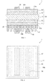
- FIG. 1 is a simplified cross-sectional view of the solar cell 1 in an embodiment.
- FIG. 2 is a simplified rear view of the solar cell 1.
- the solar cell 1 has a photoelectric conversion unit 10.
- the photoelectric conversion unit 10 is the portion which generates carriers such as electrons and holes when exposed to light.
- the photoelectric conversion unit 10 has a substrate 11, first and second semiconductor layers 12, 13, and first and second transparent conductive layers 14, 15.
- the substrate 11 is a substrate made of a semiconductor material.
- the substrate 11 has one type of conductivity.
- the substrate 11 can be constructed of a substrate made of crystalline silicon, such as a substrate of single-crystal silicon.
- the thickness of the substrate 11 can be 300 ⁇ m or less.
- the substrate 11 has first and second main surfaces 11a, 11b.
- each of the first and second main surfaces 11a, 11b has a textured structure.
- textured structure means an uneven structure formed to suppress surface reflection and increase the amount of light absorbed by the photoelectric conversion unit.
- a specific example of a textured structure is a pyramidal uneven structure (pyramid or truncated pyramid) obtained by performing anisotropic etching on the surface of a single-crystal silicon substrate having a (100) plane.
- a first semiconductor layer 12 is arranged on the first main surface 11a. Meanwhile, a second semiconductor layer 13 is formed on the second main surface 11b.
- One of the first and second semiconductor layers 12, 13 has the same type of conductivity as the substrate 11, and the other has a type of conductivity different from that of the substrate 11.
- the semiconductor layers 12, 13 can be made of p-type or n-type amorphous silicon.
- the structure of the solar cell in the present embodiment is called a HIT (registered trademark) structure.
- a substantially intrinsic i-type semiconductor layer having a thickness from several ⁇ to 250 ⁇ that does not substantially influence the generation of power may be arranged between the semiconductor layers 12, 13.
- a first transparent conductive layer 14 is arranged on the first semiconductor layer 12.
- the first transparent conductive layer 14 is provided so as to substantially cover the entire first semiconductor layer 12.
- the light-receiving surface 10a of the photoelectric conversion unit 10 is composed of the surface of the first transparent conductive layer 14.
- a linear electrode (busbar portion and finger portions) 16 made of a metal such as Ag or an alloy is arranged on the first transparent conductive layer 14. This electrode 16 collects either electron or hole carriers.
- a second transparent conductive layer 15 is arranged on the second semiconductor layer 13.
- the second transparent conductive layer 15 is provided so as to substantially cover the entire second semiconductor layer 13.
- the back surface 10b of the photoelectric conversion unit 10 is composed of the surface of the second transparent conductive layer 15.
- the light-receiving surface 10a is the main surface that primarily receives light.
- the solar cell 1 may generate electricity when receiving light only on the light-receiving surface 10a, or may be a bifacial light-receiving solar cell which generates electricity when receiving light on both the light-receiving surface 10a and the back surface 10b.
- the transparent conductive layers 14, 15 can be composed of indium tin oxide (ITO), indium zinc oxide (IZO), aluminum zinc oxide (AZO), or gallium zinc oxide (GZO).
- ITO indium tin oxide
- IZO indium zinc oxide
- AZO aluminum zinc oxide
- GZO gallium zinc oxide
- the thickness of the transparent conductive layers 14, 15 is 100 nm or less.
- layer thickness refers to the thickness in the direction normal to the surface of the layer, and not the thickness in the thickness direction of the substrate 11.
- the thickness of the transparent conductive layer 15 is thickness T 15 in FIG. 3 .
- a metal layer 17 is arranged on the second transparent conductive layer 15.
- the metal layer 17 substantially covers the entire second transparent conductive layer 15.
- a linear electrode 18 made of a metal such as Ag or an alloy is arranged on the metal layer 17.
- the electrode 18 may have a finger portion and a busbar portion. In the solar cell 1, one of the carriers, electrons or holes, is collected by electrode 18 and the metal layer 17, and the other is collected by electrode 16.
- the metal layer 17 also functions as a reflective layer. At least some of the light incident from the light-receiving surface 10a that reaches the metal layer 17 is reflected again towards the light-receiving surface 10a.
- the metal layer 17 is preferably of at least one type of metal selected from a group including Ag, Cu, Ni, Mn, Cr, Sn, Mg, W, Co and Zn. Among these a metal layer 17 of Ag is preferred.
- the thickness T 17 of the metal layer 17 is preferably from 100 nm to 400 nm, and more preferably from 150 nm to 300 nm. This increases the optical reflectance of the metal layer 17 while also reducing the electrical resistivity of the metal layer 17.
- An intermediate layer 20 is provided between the transparent conductive layer 15 and at least a portion of the metal layer 17.
- the intermediate layer 20 may be provided over the entire area in which the metal layer 17 is provided but, in the present invention, the intermediate layer 20 is arranged between the transparent conductive layer 15 and a portion of the metal layer 17. In other words, the intermediate layer 20 is arranged in a portion of the area in which the metal layer 17 is provided. More specifically, as shown in FIG. 2 , the intermediate layer 20 is provided as stripes extending parallel to each other at intervals in the area in which the metal layer 17 is provided.
- the area percentage for the area in which the intermediate layer 20 is provided relative to the area in which the metal layer 17 is provided is preferably from 20% to 80%, and more preferably from 30% to 70%.
- the intermediate layer 20 has a higher electrical resistivity than the metal layer 17.
- the electrical resistivity is determined as a general rule using carrier concentration and carrier mobility.
- the carrier concentration When the carrier concentration is higher, the electrical resistivity tends to be lower.
- the carrier concentration When the carrier concentration is lower, the electrical resistivity tends to be higher.
- the extinction coefficient is correlated with the carrier concentration, as understood from the Drude equation explained below.
- the carrier concentration is higher, the extinction coefficient is higher.
- the carrier concentration is lower, the extinction coefficient is lower.
- there is a correlation between electrical resistivity and the extinction coefficient More specifically, when the carrier concentration is high and the electrical resistivity is low, the extinction coefficient is higher. When the carrier concentration is low and the electrical resistivity is high, the extinction coefficient is lower.
- an intermediate layer 20 with an electrical resistivity that is higher than the metal layer 17 also has an extinction coefficient that is lower than the metal layer 17.
- N is the complex refractive index
- n is the refractive index
- i is an imaginary number
- k is the extinction coefficient
- E is the energy of the incident light
- A is a coefficient proportional to the carrier concentration
- ⁇ ⁇ and ⁇ are both coefficients unrelated to the carrier concentration.
- the electrical resistivity of the intermediate layer 20 is greater than the electrical resistivity of the metal layer 17 preferably by a factor of 100 or more, and more preferably by a factor of 50 or more. More specifically, the electrical resistivity of the intermediate layer 20 is preferably 1 ⁇ 10 -3 ⁇ cm or more, and more preferably 5 ⁇ 10 -3 ⁇ cm or more.
- the extinction coefficient of the intermediate layer 20 is smaller than the extinction coefficient of the metal layer 17 preferably by a factor of 0.01 or less, and more preferably by a factor of 0.002 or less. More specifically, the extinction coefficient of the intermediate layer 20 is preferably 0.1 or less, and more preferably 0.02 or less.
- the intermediate layer 20 can be made of at least one type of material selected from a group including magnesium fluoride, silicon nitride, aluminum oxide, calcium fluoride, and magnesium oxide.
- the refractive index of the intermediate layer 20 is preferably higher than the refractive index of the metal layer 17 but lower than the refractive index of the transparent conductive layer 15.
- the refractive index of the intermediate layer 20 is higher than the refractive index of the metal layer 17 preferably by 0.1 or more, and more preferably by 0.2 or more.
- the refractive index of the intermediate layer 20 is lower than the refractive index of the transparent conductive layer 15 preferably by 0.1 or more, and more preferably by 0.2 or more. More specifically, the refractive index of the intermediate layer 20 is preferably from 0.3 to 2.5, and more preferably from 1 to 2.
- the thickness T 20 of the intermediate layer 20 is preferably 100 nm or more.
- the thickness of the intermediate layer 20 is preferably less than the thickness of the metal layer 17. In other words, the thickness of the metal layer 17 is preferably greater than the thickness of the intermediate layer 20.
- a metal layer 17 functioning as a reflective layer has an electrical resistivity that is lower than the transparent conductive layer 15. Therefore, the extinction coefficient of the metal layer 17 is high. As a result, evanescent light occurring at the interface between the second semiconductor layer 13 and the transparent conductive layer 15 is readily absorbed by the metal layer 17.
- optical reflectance of the metal layer 17 is reduced by the amount of absorbed evanescent light.
- evanescent light refers to the light leaking slightly towards the transparent conductive layer 15 or the metal layer 17 when all of the light is reflected at the interface between the second semiconductor layer 13 and the transparent conductive layer 15. This evanescent light is absorbed by the transparent conductive layer 15 and the metal layer 17. Therefore, the absorption of evanescent light by the transparent conductive layer 15 and the metal layer 17 has to be taken into account when reflectance is considered. This reduces the utilization efficiency of the light. As a result, the photoelectric conversion efficiency declines.
- an intermediate layer 20 is provided between the transparent conductive layer 15 and at least a portion of the metal layer 17 in the solar cell 1.
- the intermediate layer 20 has an electrical resistivity that is higher than the metal layer 17.
- the extinction coefficient of the intermediate layer 20 is smaller than the extinction coefficient of the metal layer 17.
- the evanescent light occurring at the interface of the second semiconductor layer 13 and the transparent conductive layer 15 is less readily absorbed by the intermediate layer 20.
- the absorption of light occurring in the interface between the second semiconductor layer 13 and the transparent conductive layer 15 can be suppressed.
- reduction of the optical reflectance by the metal layer 17 can be suppressed, the utilization efficiency of light can be increased, and improved photoelectric conversion efficiency can be realized.
- the thickness of the semiconductor substrate 11 is preferably reduced, and the amount of light passing though the substrate 11 increased. More specifically, the thickness of the substrate 11 is more preferably 300 ⁇ m or less.
- Another way to prevent the metal layer 17 from being located in the area in which evanescent light generated at the interface between the second semiconductor layer 13 and the transparent conductive layer 15 is standing would be to increase the thickness of the transparent conductive layer 15. However, this increases the amount of light absorbed by the transparent conductive layer 15. This is counterproductive as it reduces the utilization efficiency of the light.
- the thickness of the transparent conductive layer 15 does not have to be increased in the solar cell 1. As a result, any increase in the amount of light absorbed by the transparent conductive layer 15 can be suppressed.
- the percentage of the area in which the intermediate layer 20 is provided is increased relative to the area in which the metal layer 17 is provided, and for the intermediate layer 20 to be substantially provided in the entire region in which the metal layer 17 is provided.
- the percentage of the area in which the intermediate layer 20 is provided is increased relative to the area in which the metal layer 17 is provided, the electrical resistivity of the intermediate layer 20 is higher than the electrical resistivity of the metal layer 17, and the resistance between the transparent conductive layer 15 and the metal layer 17 tends to increase. Therefore, the photoelectric conversion efficiency of the solar cell 1 may be reduced.
- the percentage of the area in which the intermediate layer 20 is provided relative to the area in which the metal layer 17 is provided is preferably from 20% to 80%, and more preferably from 30% to 70%.
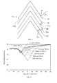
- FIG. 4 is a graph representing the reflectivity of the metal layer at an optical wavelength of 1000 nm.
- the data is obtained from a simulation performed under the following conditions.
- the thickness shown in FIG. 4 is the thickness of the intermediate layer 20.
- the horizontal axis in FIG. 4 is the angle of incidence ( ⁇ ).
- the intermediate layer 20 is provided in the entire region in which the metal layer 17 is provided.
- 2nd semiconductor layer 13 9.1 nm-thick amorphous silicon layer.
- Transparent conductive layer 15 61.5 nm-thick indium oxide layer doped with W dopant.
- Intermediate layer 20 Magnesium fluoride layer.
- Metal layer 17 400 nm-thick Ag layer.
- the optical reflectance of the metal layer 17 can be increased by providing an intermediate layer 20 with an electrical resistivity greater than that of the metal layer 17 but with an extinction coefficient that is smaller. It is also clear that the optical reflectance of the metal layer 17 can be increased even further when the thickness of the intermediate layer 20 is 100 nm or greater. From these results, it is clear that the thickness of the intermediate layer 20 is preferably 100 nm or greater.
- the thickness of the intermediate layer 20 is preferably smaller than the thickness of the metal layer 17. In other words, the thickness of the metal layer 17 is preferably greater than the thickness of the intermediate layer 20.
- FIG. 5 is a graph representing the reflectivity of the metal layer of the solar cell in the present embodiment at an optical wavelength of 1000 nm.
- the data shown in FIG. 5 the data is obtained from a simulation performed under the following conditions.
- the thickness shown in FIG. 5 is the thickness of the transparent conductive layer 15.
- the intermediate layer 20 is provided in the entire region in which the metal layer 17.
- 2nd semiconductor layer 13 9.1 nm-thick amorphous silicon layer.
- Transparent conductive layer 15 indium oxide layer doped with W dopant.
- Intermediate layer 20 61.5 nm-thick magnesium fluoride layer.
- Metal layer 17 400 nm-thick Ag layer.
- FIG. 6 is a graph representing the reflectivity at an optical wavelength of 1000 nm of the metal layer of a solar cell in a reference example having a configuration substantially identical to the solar cell in the embodiment, except that an intermediate layer 20 is not provided.
- the thickness shown in FIG. 6 is the thickness of the transparent conductive layer.
- the thickness of the transparent conductive layer 15 is preferably 100 nm or less when an intermediate layer 20 is provided.
- the refractive index of the intermediate layer 20 is preferably higher than the refractive index of the metal layer 17 but lower than the refractive index of the transparent conductive layer 15.
- the light interference effect increases the reflectance.
- the intermediate layer 20 may be provided over the entire area in which the metal layer 17 is provided. In this case, the absorption of evanescent light can be more effectively suppressed.
- the photoelectric conversion unit does not have to have a HIT structure.
- Polycrystalline silicon, thin-film silicon, or CIGS may be used.
- the solar cell may also be a back contact solar cell in which the first and second electrodes are arranged on a single main surface.
Landscapes
- Photovoltaic Devices (AREA)
- Life Sciences & Earth Sciences (AREA)
- Engineering & Computer Science (AREA)
- Sustainable Development (AREA)
- Sustainable Energy (AREA)
Abstract
Description
- The present invention relates to a solar cell.
- Solar cells have attracted attention in recent years as an energy source with a low environmental impact. A solar cell is described in
Patent Document 1 which has a semiconductor substrate, a silicon layer arranged on the main surface of the semiconductor substrate on the back surface side, a transparent conductive layer arranged on the silicon layer, and a reflective layer of Ag arranged on the transparent conductive layer. - Patent Document 1: PCT Application Translation No.
8-508368 - There has been growing demand in recent years for a solar cell with even greater photoelectric conversion efficiency.
- The present invention provides a solar cell with improved photoelectric conversion efficiency.
- The solar cell of the present invention includes a photoelectric conversion unit, a metal layer, and an intermediate layer. The photoelectric conversion unit includes a transparent conductive layer on a surface. The metal layer is arranged on the transparent conductive layer. The intermediate layer is arranged between the metal layer and the transparent conductive layer. The intermediate layer has a smaller extinction coefficient than that of the metal layer.
- The present invention is able to provide a solar cell with improved photoelectric conversion efficiency.
-
-
FIG. 1 is a simplified cross-sectional view of the solar cell in an embodiment. -
FIG. 2 is a simplified rear view of the solar cell in the embodiment. -
FIG. 3 is a simplified cross-sectional view in which a portion of the solar cell in the embodiment has been enlarged. InFIG. 3 , the cross-sectional hatching has been omitted. -
FIG. 4 is a graph representing the optical reflectance of the metal layer of the solar cell in the embodiment at an optical wavelength of 1000 nm. -
FIG. 5 is a graph representing the reflectivity of the metal layer of the solar cell in the embodiment at an optical wavelength of 1000 nm. -
FIG. 6 is a graph representing the reflectivity of the metal layer of the solar cell in a reference example at an optical wavelength of 1000 nm. - The following is an explanation of examples of preferred embodiments of the present invention. The following embodiments are merely examples. The present invention is not limited by the following embodiments in any way.
- Further, in each of the drawings referenced in the embodiments, members having substantially the same function are denoted by the same symbols. The drawings referenced in the embodiments are also depicted schematically. The dimensional ratios of the objects depicted in the drawings may differ from those of the actual objects. The dimensional ratios of objects may also vary between drawings. The specific dimensional ratios of the objects should be determined with reference to the following explanation.
-
FIG. 1 is a simplified cross-sectional view of thesolar cell 1 in an embodiment.FIG. 2 is a simplified rear view of thesolar cell 1. - The
solar cell 1 has aphotoelectric conversion unit 10. Thephotoelectric conversion unit 10 is the portion which generates carriers such as electrons and holes when exposed to light. Thephotoelectric conversion unit 10 has asubstrate 11, first andsecond semiconductor layers conductive layers - The
substrate 11 is a substrate made of a semiconductor material. Thesubstrate 11 has one type of conductivity. Thesubstrate 11 can be constructed of a substrate made of crystalline silicon, such as a substrate of single-crystal silicon. The thickness of thesubstrate 11 can be 300 µm or less. Thesubstrate 11 has first and secondmain surfaces - In the present embodiment, as shown in
FIG. 3 , each of the first and secondmain surfaces - A
first semiconductor layer 12 is arranged on the firstmain surface 11a. Meanwhile, asecond semiconductor layer 13 is formed on the secondmain surface 11b. One of the first andsecond semiconductor layers substrate 11, and the other has a type of conductivity different from that of thesubstrate 11. Thesemiconductor layers - A substantially intrinsic i-type semiconductor layer having a thickness from several Å to 250 Å that does not substantially influence the generation of power may be arranged between the
semiconductor layers - A first transparent
conductive layer 14 is arranged on thefirst semiconductor layer 12. The first transparentconductive layer 14 is provided so as to substantially cover the entirefirst semiconductor layer 12. The light-receivingsurface 10a of thephotoelectric conversion unit 10 is composed of the surface of the first transparentconductive layer 14. - A linear electrode (busbar portion and finger portions) 16 made of a metal such as Ag or an alloy is arranged on the first transparent
conductive layer 14. Thiselectrode 16 collects either electron or hole carriers. - A second transparent
conductive layer 15 is arranged on thesecond semiconductor layer 13. The second transparentconductive layer 15 is provided so as to substantially cover the entiresecond semiconductor layer 13. Theback surface 10b of thephotoelectric conversion unit 10 is composed of the surface of the second transparentconductive layer 15. The light-receivingsurface 10a is the main surface that primarily receives light. Thesolar cell 1 may generate electricity when receiving light only on the light-receivingsurface 10a, or may be a bifacial light-receiving solar cell which generates electricity when receiving light on both the light-receivingsurface 10a and theback surface 10b. - The transparent
conductive layers - The thickness of the transparent
conductive layers substrate 11. Specifically, the thickness of the transparentconductive layer 15 is thickness T15 inFIG. 3 . - A
metal layer 17 is arranged on the second transparentconductive layer 15. Themetal layer 17 substantially covers the entire second transparentconductive layer 15. Alinear electrode 18 made of a metal such as Ag or an alloy is arranged on themetal layer 17. Theelectrode 18 may have a finger portion and a busbar portion. In thesolar cell 1, one of the carriers, electrons or holes, is collected byelectrode 18 and themetal layer 17, and the other is collected byelectrode 16. - The
metal layer 17 also functions as a reflective layer. At least some of the light incident from the light-receivingsurface 10a that reaches themetal layer 17 is reflected again towards the light-receivingsurface 10a. - The
metal layer 17 is preferably of at least one type of metal selected from a group including Ag, Cu, Ni, Mn, Cr, Sn, Mg, W, Co and Zn. Among these ametal layer 17 of Ag is preferred. - The thickness T17 of the
metal layer 17 is preferably from 100 nm to 400 nm, and more preferably from 150 nm to 300 nm. This increases the optical reflectance of themetal layer 17 while also reducing the electrical resistivity of themetal layer 17. - An
intermediate layer 20 is provided between the transparentconductive layer 15 and at least a portion of themetal layer 17. Theintermediate layer 20 may be provided over the entire area in which themetal layer 17 is provided but, in the present invention, theintermediate layer 20 is arranged between the transparentconductive layer 15 and a portion of themetal layer 17. In other words, theintermediate layer 20 is arranged in a portion of the area in which themetal layer 17 is provided. More specifically, as shown inFIG. 2 , theintermediate layer 20 is provided as stripes extending parallel to each other at intervals in the area in which themetal layer 17 is provided. - From the standpoint of reducing the electrical resistivity, the area percentage for the area in which the
intermediate layer 20 is provided relative to the area in which themetal layer 17 is provided is preferably from 20% to 80%, and more preferably from 30% to 70%. - The
intermediate layer 20 has a higher electrical resistivity than themetal layer 17. Here, the electrical resistivity is determined as a general rule using carrier concentration and carrier mobility. When the carrier concentration is higher, the electrical resistivity tends to be lower. When the carrier concentration is lower, the electrical resistivity tends to be higher. However, the extinction coefficient is correlated with the carrier concentration, as understood from the Drude equation explained below. When the carrier concentration is higher, the extinction coefficient is higher. When the carrier concentration is lower, the extinction coefficient is lower. In other words, there is a correlation between electrical resistivity and the extinction coefficient. More specifically, when the carrier concentration is high and the electrical resistivity is low, the extinction coefficient is higher. When the carrier concentration is low and the electrical resistivity is high, the extinction coefficient is lower. Therefore, anintermediate layer 20 with an electrical resistivity that is higher than themetal layer 17 also has an extinction coefficient that is lower than themetal layer 17.
- In the Drude equation, N is the complex refractive index, n is the refractive index, i is an imaginary number, k is the extinction coefficient, E is the energy of the incident light, A is a coefficient proportional to the carrier concentration, and ε∞ and Γ are both coefficients unrelated to the carrier concentration.
- The electrical resistivity of the
intermediate layer 20 is greater than the electrical resistivity of themetal layer 17 preferably by a factor of 100 or more, and more preferably by a factor of 50 or more. More specifically, the electrical resistivity of theintermediate layer 20 is preferably 1 × 10⁻³ Ω·cm or more, and more preferably 5 × 10⁻³ Ω·cm or more. - The extinction coefficient of the
intermediate layer 20 is smaller than the extinction coefficient of themetal layer 17 preferably by a factor of 0.01 or less, and more preferably by a factor of 0.002 or less. More specifically, the extinction coefficient of theintermediate layer 20 is preferably 0.1 or less, and more preferably 0.02 or less. - The
intermediate layer 20 can be made of at least one type of material selected from a group including magnesium fluoride, silicon nitride, aluminum oxide, calcium fluoride, and magnesium oxide. - The refractive index of the
intermediate layer 20 is preferably higher than the refractive index of themetal layer 17 but lower than the refractive index of the transparentconductive layer 15. The refractive index of theintermediate layer 20 is higher than the refractive index of themetal layer 17 preferably by 0.1 or more, and more preferably by 0.2 or more. The refractive index of theintermediate layer 20 is lower than the refractive index of the transparentconductive layer 15 preferably by 0.1 or more, and more preferably by 0.2 or more. More specifically, the refractive index of theintermediate layer 20 is preferably from 0.3 to 2.5, and more preferably from 1 to 2. - The thickness T20 of the
intermediate layer 20 is preferably 100 nm or more. The thickness of theintermediate layer 20 is preferably less than the thickness of themetal layer 17. In other words, the thickness of themetal layer 17 is preferably greater than the thickness of theintermediate layer 20. - However, a
metal layer 17 functioning as a reflective layer has an electrical resistivity that is lower than the transparentconductive layer 15. Therefore, the extinction coefficient of themetal layer 17 is high. As a result, evanescent light occurring at the interface between thesecond semiconductor layer 13 and the transparentconductive layer 15 is readily absorbed by themetal layer 17. When evanescent light is absorbed by themetal layer 17, optical reflectance of themetal layer 17 is reduced by the amount of absorbed evanescent light. Here, evanescent light refers to the light leaking slightly towards the transparentconductive layer 15 or themetal layer 17 when all of the light is reflected at the interface between thesecond semiconductor layer 13 and the transparentconductive layer 15. This evanescent light is absorbed by the transparentconductive layer 15 and themetal layer 17. Therefore, the absorption of evanescent light by the transparentconductive layer 15 and themetal layer 17 has to be taken into account when reflectance is considered. This reduces the utilization efficiency of the light. As a result, the photoelectric conversion efficiency declines. - For this reason, an
intermediate layer 20 is provided between the transparentconductive layer 15 and at least a portion of themetal layer 17 in thesolar cell 1. Theintermediate layer 20 has an electrical resistivity that is higher than themetal layer 17. Thus, the extinction coefficient of theintermediate layer 20 is smaller than the extinction coefficient of themetal layer 17. As a result, the evanescent light occurring at the interface of thesecond semiconductor layer 13 and the transparentconductive layer 15 is less readily absorbed by theintermediate layer 20. By arranging thisintermediate layer 20 between themetal layer 17 and the transparentconductive layer 15, the percentage of the area in which themetal layer 17 readily absorbs evanescent light can be reduced relative to the area in which evanescent light is standing. Therefore, the absorption of light occurring in the interface between thesecond semiconductor layer 13 and the transparentconductive layer 15 can be suppressed. As a result, reduction of the optical reflectance by themetal layer 17 can be suppressed, the utilization efficiency of light can be increased, and improved photoelectric conversion efficiency can be realized. - In an embodiment able to increase the optical reflectance of the
metal layer 17 and improve the utilization efficiency of light, the thickness of thesemiconductor substrate 11 is preferably reduced, and the amount of light passing though thesubstrate 11 increased. More specifically, the thickness of thesubstrate 11 is more preferably 300 µm or less. - Another way to prevent the
metal layer 17 from being located in the area in which evanescent light generated at the interface between thesecond semiconductor layer 13 and the transparentconductive layer 15 is standing would be to increase the thickness of the transparentconductive layer 15. However, this increases the amount of light absorbed by the transparentconductive layer 15. This is counterproductive as it reduces the utilization efficiency of the light. - In contrast, the thickness of the transparent
conductive layer 15 does not have to be increased in thesolar cell 1. As a result, any increase in the amount of light absorbed by the transparentconductive layer 15 can be suppressed. - From the standpoint of more effectively suppressing the absorption of light by the
metal layer 17, it is preferable for the percentage of the area in which theintermediate layer 20 is provided to be increased relative to the area in which themetal layer 17 is provided, and for theintermediate layer 20 to be substantially provided in the entire region in which themetal layer 17 is provided. However, when the percentage of the area in which theintermediate layer 20 is provided is increased relative to the area in which themetal layer 17 is provided, the electrical resistivity of theintermediate layer 20 is higher than the electrical resistivity of themetal layer 17, and the resistance between the transparentconductive layer 15 and themetal layer 17 tends to increase. Therefore, the photoelectric conversion efficiency of thesolar cell 1 may be reduced. From this standpoint, the percentage of the area in which theintermediate layer 20 is provided relative to the area in which themetal layer 17 is provided is preferably from 20% to 80%, and more preferably from 30% to 70%. -
FIG. 4 is a graph representing the reflectivity of the metal layer at an optical wavelength of 1000 nm. In the graph shown inFIG. 4 , the data is obtained from a simulation performed under the following conditions. The thickness shown inFIG. 4 is the thickness of theintermediate layer 20. The horizontal axis inFIG. 4 is the angle of incidence (θ). - The
intermediate layer 20 is provided in the entire region in which themetal layer 17 is provided. - 2nd semiconductor layer 13: 9.1 nm-thick amorphous silicon layer.
- Transparent conductive layer 15: 61.5 nm-thick indium oxide layer doped with W dopant.
- Intermediate layer 20: Magnesium fluoride layer.
- Metal layer 17: 400 nm-thick Ag layer.
- It is clear from the graph shown in
FIG. 4 that the optical reflectance of themetal layer 17 can be increased by providing anintermediate layer 20 with an electrical resistivity greater than that of themetal layer 17 but with an extinction coefficient that is smaller. It is also clear that the optical reflectance of themetal layer 17 can be increased even further when the thickness of theintermediate layer 20 is 100 nm or greater. From these results, it is clear that the thickness of theintermediate layer 20 is preferably 100 nm or greater. However, when theintermediate layer 20 is too thick and theintermediate layer 20 is thicker than themetal layer 17, the portion in which themetal layer 17 is positioned above theintermediate layer 20 and the portion in which themetal layer 17 is positioned in the region where theintermediate layer 20 is not provided may become decoupled in themetal layer 17 forming process due to a coverage problem. Therefore, the thickness of theintermediate layer 20 is preferably smaller than the thickness of themetal layer 17. In other words, the thickness of themetal layer 17 is preferably greater than the thickness of theintermediate layer 20. -
FIG. 5 is a graph representing the reflectivity of the metal layer of the solar cell in the present embodiment at an optical wavelength of 1000 nm. In the data shown inFIG. 5 , the data is obtained from a simulation performed under the following conditions. The thickness shown inFIG. 5 is the thickness of the transparentconductive layer 15. - The
intermediate layer 20 is provided in the entire region in which themetal layer 17. - 2nd semiconductor layer 13: 9.1 nm-thick amorphous silicon layer.
- Transparent conductive layer 15: indium oxide layer doped with W dopant.
- Intermediate layer 20: 61.5 nm-thick magnesium fluoride layer.
- Metal layer 17: 400 nm-thick Ag layer.
-
FIG. 6 is a graph representing the reflectivity at an optical wavelength of 1000 nm of the metal layer of a solar cell in a reference example having a configuration substantially identical to the solar cell in the embodiment, except that anintermediate layer 20 is not provided. The thickness shown inFIG. 6 is the thickness of the transparent conductive layer. - It is clear from the graphs in
FIG. 5 and FIG. 6 that when anintermediate layer 20 is provided the minimum value of optical reflectance decreases monotonically as the thickness of the transparentconductive layer 15 increases. This does not occur when anintermediate layer 20 is not provided. It is clear from these results that the thickness of the transparentconductive layer 15 is preferably 100 nm or less when anintermediate layer 20 is provided. - Also, the refractive index of the
intermediate layer 20 is preferably higher than the refractive index of themetal layer 17 but lower than the refractive index of the transparentconductive layer 15. Here, the light interference effect increases the reflectance. - The present invention includes many embodiments not described herein. For example, the
intermediate layer 20 may be provided over the entire area in which themetal layer 17 is provided. In this case, the absorption of evanescent light can be more effectively suppressed. - The photoelectric conversion unit does not have to have a HIT structure.
- Polycrystalline silicon, thin-film silicon, or CIGS may be used.
- The solar cell may also be a back contact solar cell in which the first and second electrodes are arranged on a single main surface.
- The present invention includes many other embodiments not described herein. Therefore, the technical scope of the present invention is defined solely by the items of the invention specified in the claims pertinent to the above explanation.
-
- 1:
- Solar cell
- 10:
- Photoelectric conversion unit
- 11:
- Substrate
- 12:
- 1 st semiconductor layer
- 13:
- 2nd semiconductor layer
- 14:
- 1 st transparent conductive layer
- 15:
- 2nd transparent conductive layer
- 17:
- Metal layer
- 20:
- Intermediate layer
Claims (8)
- A solar cell comprising:a photoelectric conversion unit including a transparent conductive layer on a surface;a metal layer arranged on the transparent conductive layer; andan intermediate layer arranged between the metal layer and the transparent conductive layer, the intermediate layer having a smaller extinction coefficient than the metal layer.
- The solar cell according to claim 1, wherein the intermediate layer has a higher electrical resistivity than the metal layer, and is arranged between the transparent conductive layer and a portion of the metal layer.
- The solar cell according to claim 2, wherein the area ratio of the area in which the intermediate layer is provided relative to the area in which the metal layer is provided is from 20% to 80%.
- The solar cell according to claim 2 or claim 3, wherein the thickness of the metal layer is greater than the thickness of the intermediate layer.
- The solar cell according to any one of claims 1 through 4, wherein the refractive index of the intermediate layer is greater than the refractive index of the metal layer, but less than the refractive index of the transparent conductive layer.
- The solar cell according to any one of claims 1 through 5, wherein the intermediate layer is made of at least one type of material selected from a group including magnesium fluoride, silicon nitride, aluminum oxide, calcium fluoride, and magnesium oxide.
- The solar cell according to any one of claims 1 through 6, wherein the metal layer is made of at least one type of element selected from a group including Ag, Cu, Ni, Mn, Cr, Sn, Mg, W, Co, and Zn.
- The solar cell according to any one of claims 1 through 7, wherein the photoelectric conversion unit includes a substrate made of crystalline silicon, and the thickness of the substrate is 300 µm or less.
Applications Claiming Priority (2)
| Application Number | Priority Date | Filing Date | Title |
|---|---|---|---|
| JP2011163823A JP2013030520A (en) | 2011-07-27 | 2011-07-27 | Solar cell |
| PCT/JP2012/056859 WO2013014967A1 (en) | 2011-07-27 | 2012-03-16 | Solar cell |
Publications (3)
| Publication Number | Publication Date |
|---|---|
| EP2738819A1 true EP2738819A1 (en) | 2014-06-04 |
| EP2738819A4 EP2738819A4 (en) | 2015-04-08 |
| EP2738819B1 EP2738819B1 (en) | 2018-05-30 |
Family
ID=47600827
Family Applications (1)
| Application Number | Title | Priority Date | Filing Date |
|---|---|---|---|
| EP12817558.5A Not-in-force EP2738819B1 (en) | 2011-07-27 | 2012-03-16 | Solar cell |
Country Status (4)
| Country | Link |
|---|---|
| US (1) | US20140130861A1 (en) |
| EP (1) | EP2738819B1 (en) |
| JP (1) | JP2013030520A (en) |
| WO (1) | WO2013014967A1 (en) |
Families Citing this family (2)
| Publication number | Priority date | Publication date | Assignee | Title |
|---|---|---|---|---|
| JP2015073057A (en) * | 2013-10-04 | 2015-04-16 | 長州産業株式会社 | Photovoltaic element |
| JP2019179838A (en) * | 2018-03-30 | 2019-10-17 | パナソニック株式会社 | Solar cell, and manufacturing method of solar cell |
Family Cites Families (12)
| Publication number | Priority date | Publication date | Assignee | Title |
|---|---|---|---|---|
| FR2711276B1 (en) * | 1993-10-11 | 1995-12-01 | Neuchatel Universite | Photovoltaic cell and method of manufacturing such a cell. |
| JPH07321362A (en) * | 1994-05-24 | 1995-12-08 | Sanyo Electric Co Ltd | Photovoltaic device |
| US5569332A (en) * | 1995-08-07 | 1996-10-29 | United Solar Systems Corporation | Optically enhanced photovoltaic back reflector |
| JP3193287B2 (en) * | 1996-02-28 | 2001-07-30 | シャープ株式会社 | Solar cell |
| JPH11220154A (en) * | 1997-10-29 | 1999-08-10 | Canon Inc | Photovoltaic element and photovoltaic element module |
| EP0915523A3 (en) * | 1997-10-29 | 2005-11-02 | Canon Kabushiki Kaisha | A photovoltaic element having a back side transparent and electrically conductive layer with a light incident side surface region having a specific cross section and a module comprising said photovoltaic element |
| WO2006005889A1 (en) * | 2004-07-07 | 2006-01-19 | Saint-Gobain Glass France | Photovoltaic solar cell and solar module |
| DE102004032810B4 (en) * | 2004-07-07 | 2009-01-08 | Saint-Gobain Glass Deutschland Gmbh | Photovoltaic solar cell with a layer of light-scattering properties and solar module |
| WO2008059857A1 (en) * | 2006-11-17 | 2008-05-22 | Kaneka Corporation | Thin-film photoelectric conversion device |
| CN101978508A (en) * | 2008-03-19 | 2011-02-16 | 三洋电机株式会社 | Solar cell and manufacturing method thereof |
| JP2009231505A (en) * | 2008-03-21 | 2009-10-08 | Sanyo Electric Co Ltd | Solar battery |
| JP5535709B2 (en) * | 2010-03-19 | 2014-07-02 | 三洋電機株式会社 | SOLAR CELL, SOLAR CELL MODULE USING THE SOLAR CELL, AND SOLAR CELL MANUFACTURING METHOD |
-
2011
- 2011-07-27 JP JP2011163823A patent/JP2013030520A/en active Pending
-
2012
- 2012-03-16 WO PCT/JP2012/056859 patent/WO2013014967A1/en not_active Ceased
- 2012-03-16 EP EP12817558.5A patent/EP2738819B1/en not_active Not-in-force
-
2014
- 2014-01-21 US US14/159,677 patent/US20140130861A1/en not_active Abandoned
Also Published As
| Publication number | Publication date |
|---|---|
| US20140130861A1 (en) | 2014-05-15 |
| JP2013030520A (en) | 2013-02-07 |
| EP2738819B1 (en) | 2018-05-30 |
| EP2738819A4 (en) | 2015-04-08 |
| WO2013014967A1 (en) | 2013-01-31 |
Similar Documents
| Publication | Publication Date | Title |
|---|---|---|
| EP2867926B1 (en) | Solar cell | |
| JP4257332B2 (en) | Silicon-based thin film solar cell | |
| US10084107B2 (en) | Transparent conducting oxide for photovoltaic devices | |
| JP5705968B2 (en) | Photoelectric conversion device and manufacturing method thereof | |
| JP4940309B2 (en) | Solar cell | |
| US20080236661A1 (en) | Solar cell | |
| KR20110122704A (en) | Photovoltaic module with semiconductor multilayer stack and manufacturing method of photovoltaic module | |
| JP2011035092A (en) | Back-junction type solar cell and solar cell module using the same | |
| US20110155210A1 (en) | Solar cell module | |
| EP2672522A1 (en) | Photoelectric conversion element | |
| JP6414767B2 (en) | Solar cells | |
| KR20150090606A (en) | Solar cell and manufacturing method thereof | |
| US20120006391A1 (en) | Photovoltaic module and method of manufacturing a photovoltaic module having an electrode diffusion layer | |
| EP2738819B1 (en) | Solar cell | |
| EP2273559A1 (en) | Solar cell | |
| US9627557B2 (en) | Solar cell | |
| WO2011105170A1 (en) | Solar cell | |
| US9040812B2 (en) | Photovoltaic device including flexible substrate or inflexible substrate and method for manufacturing the same | |
| JP5542025B2 (en) | Photoelectric conversion device | |
| JP5371284B2 (en) | Thin film photoelectric converter | |
| TW201414001A (en) | Deliberately doped cadmium oxide layer for solar cells | |
| EP2608273A2 (en) | Solar cell having a pn hetero-junction | |
| US20120055535A1 (en) | Photovoltaic Devices With Textured Glass Superstrate | |
| US20100258171A1 (en) | Solar photovoltaic device | |
| US20100154882A1 (en) | Solar cell |
Legal Events
| Date | Code | Title | Description |
|---|---|---|---|
| PUAI | Public reference made under article 153(3) epc to a published international application that has entered the european phase |
Free format text: ORIGINAL CODE: 0009012 |
|
| 17P | Request for examination filed |
Effective date: 20140212 |
|
| AK | Designated contracting states |
Kind code of ref document: A1 Designated state(s): AL AT BE BG CH CY CZ DE DK EE ES FI FR GB GR HR HU IE IS IT LI LT LU LV MC MK MT NL NO PL PT RO RS SE SI SK SM TR |
|
| DAX | Request for extension of the european patent (deleted) | ||
| RA4 | Supplementary search report drawn up and despatched (corrected) |
Effective date: 20150310 |
|
| RIC1 | Information provided on ipc code assigned before grant |
Ipc: H01L 31/056 20140101ALI20150304BHEP Ipc: H01L 31/0747 20120101ALI20150304BHEP Ipc: H01L 31/04 20140101AFI20150304BHEP Ipc: H01L 31/0224 20060101ALI20150304BHEP |
|
| RAP1 | Party data changed (applicant data changed or rights of an application transferred) |
Owner name: PANASONIC INTELLECTUAL PROPERTY MANAGEMENT CO., LT |
|
| GRAP | Despatch of communication of intention to grant a patent |
Free format text: ORIGINAL CODE: EPIDOSNIGR1 |
|
| STAA | Information on the status of an ep patent application or granted ep patent |
Free format text: STATUS: GRANT OF PATENT IS INTENDED |
|
| INTG | Intention to grant announced |
Effective date: 20180102 |
|
| GRAS | Grant fee paid |
Free format text: ORIGINAL CODE: EPIDOSNIGR3 |
|
| GRAA | (expected) grant |
Free format text: ORIGINAL CODE: 0009210 |
|
| STAA | Information on the status of an ep patent application or granted ep patent |
Free format text: STATUS: THE PATENT HAS BEEN GRANTED |
|
| AK | Designated contracting states |
Kind code of ref document: B1 Designated state(s): AL AT BE BG CH CY CZ DE DK EE ES FI FR GB GR HR HU IE IS IT LI LT LU LV MC MK MT NL NO PL PT RO RS SE SI SK SM TR |
|
| REG | Reference to a national code |
Ref country code: GB Ref legal event code: FG4D |
|
| REG | Reference to a national code |
Ref country code: CH Ref legal event code: EP |
|
| REG | Reference to a national code |
Ref country code: AT Ref legal event code: REF Ref document number: 1004484 Country of ref document: AT Kind code of ref document: T Effective date: 20180615 |
|
| REG | Reference to a national code |
Ref country code: IE Ref legal event code: FG4D |
|
| REG | Reference to a national code |
Ref country code: DE Ref legal event code: R096 Ref document number: 602012047005 Country of ref document: DE |
|
| REG | Reference to a national code |
Ref country code: NL Ref legal event code: MP Effective date: 20180530 |
|
| REG | Reference to a national code |
Ref country code: LT Ref legal event code: MG4D |
|
| PG25 | Lapsed in a contracting state [announced via postgrant information from national office to epo] |
Ref country code: BG Free format text: LAPSE BECAUSE OF FAILURE TO SUBMIT A TRANSLATION OF THE DESCRIPTION OR TO PAY THE FEE WITHIN THE PRESCRIBED TIME-LIMIT Effective date: 20180830 Ref country code: FI Free format text: LAPSE BECAUSE OF FAILURE TO SUBMIT A TRANSLATION OF THE DESCRIPTION OR TO PAY THE FEE WITHIN THE PRESCRIBED TIME-LIMIT Effective date: 20180530 Ref country code: SE Free format text: LAPSE BECAUSE OF FAILURE TO SUBMIT A TRANSLATION OF THE DESCRIPTION OR TO PAY THE FEE WITHIN THE PRESCRIBED TIME-LIMIT Effective date: 20180530 Ref country code: NO Free format text: LAPSE BECAUSE OF FAILURE TO SUBMIT A TRANSLATION OF THE DESCRIPTION OR TO PAY THE FEE WITHIN THE PRESCRIBED TIME-LIMIT Effective date: 20180830 Ref country code: ES Free format text: LAPSE BECAUSE OF FAILURE TO SUBMIT A TRANSLATION OF THE DESCRIPTION OR TO PAY THE FEE WITHIN THE PRESCRIBED TIME-LIMIT Effective date: 20180530 Ref country code: LT Free format text: LAPSE BECAUSE OF FAILURE TO SUBMIT A TRANSLATION OF THE DESCRIPTION OR TO PAY THE FEE WITHIN THE PRESCRIBED TIME-LIMIT Effective date: 20180530 Ref country code: CY Free format text: LAPSE BECAUSE OF FAILURE TO SUBMIT A TRANSLATION OF THE DESCRIPTION OR TO PAY THE FEE WITHIN THE PRESCRIBED TIME-LIMIT Effective date: 20180530 |
|
| PG25 | Lapsed in a contracting state [announced via postgrant information from national office to epo] |
Ref country code: HR Free format text: LAPSE BECAUSE OF FAILURE TO SUBMIT A TRANSLATION OF THE DESCRIPTION OR TO PAY THE FEE WITHIN THE PRESCRIBED TIME-LIMIT Effective date: 20180530 Ref country code: RS Free format text: LAPSE BECAUSE OF FAILURE TO SUBMIT A TRANSLATION OF THE DESCRIPTION OR TO PAY THE FEE WITHIN THE PRESCRIBED TIME-LIMIT Effective date: 20180530 Ref country code: GR Free format text: LAPSE BECAUSE OF FAILURE TO SUBMIT A TRANSLATION OF THE DESCRIPTION OR TO PAY THE FEE WITHIN THE PRESCRIBED TIME-LIMIT Effective date: 20180831 Ref country code: LV Free format text: LAPSE BECAUSE OF FAILURE TO SUBMIT A TRANSLATION OF THE DESCRIPTION OR TO PAY THE FEE WITHIN THE PRESCRIBED TIME-LIMIT Effective date: 20180530 |
|
| REG | Reference to a national code |
Ref country code: AT Ref legal event code: MK05 Ref document number: 1004484 Country of ref document: AT Kind code of ref document: T Effective date: 20180530 |
|
| PG25 | Lapsed in a contracting state [announced via postgrant information from national office to epo] |
Ref country code: NL Free format text: LAPSE BECAUSE OF FAILURE TO SUBMIT A TRANSLATION OF THE DESCRIPTION OR TO PAY THE FEE WITHIN THE PRESCRIBED TIME-LIMIT Effective date: 20180530 |
|
| PG25 | Lapsed in a contracting state [announced via postgrant information from national office to epo] |
Ref country code: EE Free format text: LAPSE BECAUSE OF FAILURE TO SUBMIT A TRANSLATION OF THE DESCRIPTION OR TO PAY THE FEE WITHIN THE PRESCRIBED TIME-LIMIT Effective date: 20180530 Ref country code: SK Free format text: LAPSE BECAUSE OF FAILURE TO SUBMIT A TRANSLATION OF THE DESCRIPTION OR TO PAY THE FEE WITHIN THE PRESCRIBED TIME-LIMIT Effective date: 20180530 Ref country code: AT Free format text: LAPSE BECAUSE OF FAILURE TO SUBMIT A TRANSLATION OF THE DESCRIPTION OR TO PAY THE FEE WITHIN THE PRESCRIBED TIME-LIMIT Effective date: 20180530 Ref country code: DK Free format text: LAPSE BECAUSE OF FAILURE TO SUBMIT A TRANSLATION OF THE DESCRIPTION OR TO PAY THE FEE WITHIN THE PRESCRIBED TIME-LIMIT Effective date: 20180530 Ref country code: CZ Free format text: LAPSE BECAUSE OF FAILURE TO SUBMIT A TRANSLATION OF THE DESCRIPTION OR TO PAY THE FEE WITHIN THE PRESCRIBED TIME-LIMIT Effective date: 20180530 Ref country code: RO Free format text: LAPSE BECAUSE OF FAILURE TO SUBMIT A TRANSLATION OF THE DESCRIPTION OR TO PAY THE FEE WITHIN THE PRESCRIBED TIME-LIMIT Effective date: 20180530 Ref country code: PL Free format text: LAPSE BECAUSE OF FAILURE TO SUBMIT A TRANSLATION OF THE DESCRIPTION OR TO PAY THE FEE WITHIN THE PRESCRIBED TIME-LIMIT Effective date: 20180530 |
|
| PG25 | Lapsed in a contracting state [announced via postgrant information from national office to epo] |
Ref country code: SM Free format text: LAPSE BECAUSE OF FAILURE TO SUBMIT A TRANSLATION OF THE DESCRIPTION OR TO PAY THE FEE WITHIN THE PRESCRIBED TIME-LIMIT Effective date: 20180530 Ref country code: IT Free format text: LAPSE BECAUSE OF FAILURE TO SUBMIT A TRANSLATION OF THE DESCRIPTION OR TO PAY THE FEE WITHIN THE PRESCRIBED TIME-LIMIT Effective date: 20180530 |
|
| REG | Reference to a national code |
Ref country code: DE Ref legal event code: R097 Ref document number: 602012047005 Country of ref document: DE |
|
| PLBE | No opposition filed within time limit |
Free format text: ORIGINAL CODE: 0009261 |
|
| STAA | Information on the status of an ep patent application or granted ep patent |
Free format text: STATUS: NO OPPOSITION FILED WITHIN TIME LIMIT |
|
| 26N | No opposition filed |
Effective date: 20190301 |
|
| PG25 | Lapsed in a contracting state [announced via postgrant information from national office to epo] |
Ref country code: SI Free format text: LAPSE BECAUSE OF FAILURE TO SUBMIT A TRANSLATION OF THE DESCRIPTION OR TO PAY THE FEE WITHIN THE PRESCRIBED TIME-LIMIT Effective date: 20180530 |
|
| PG25 | Lapsed in a contracting state [announced via postgrant information from national office to epo] |
Ref country code: MC Free format text: LAPSE BECAUSE OF FAILURE TO SUBMIT A TRANSLATION OF THE DESCRIPTION OR TO PAY THE FEE WITHIN THE PRESCRIBED TIME-LIMIT Effective date: 20180530 |
|
| REG | Reference to a national code |
Ref country code: CH Ref legal event code: PL |
|
| GBPC | Gb: european patent ceased through non-payment of renewal fee |
Effective date: 20190316 |
|
| PG25 | Lapsed in a contracting state [announced via postgrant information from national office to epo] |
Ref country code: AL Free format text: LAPSE BECAUSE OF FAILURE TO SUBMIT A TRANSLATION OF THE DESCRIPTION OR TO PAY THE FEE WITHIN THE PRESCRIBED TIME-LIMIT Effective date: 20180530 Ref country code: LU Free format text: LAPSE BECAUSE OF NON-PAYMENT OF DUE FEES Effective date: 20190316 |
|
| REG | Reference to a national code |
Ref country code: BE Ref legal event code: MM Effective date: 20190331 |
|
| PG25 | Lapsed in a contracting state [announced via postgrant information from national office to epo] |
Ref country code: LI Free format text: LAPSE BECAUSE OF NON-PAYMENT OF DUE FEES Effective date: 20190331 Ref country code: CH Free format text: LAPSE BECAUSE OF NON-PAYMENT OF DUE FEES Effective date: 20190331 Ref country code: GB Free format text: LAPSE BECAUSE OF NON-PAYMENT OF DUE FEES Effective date: 20190316 Ref country code: IE Free format text: LAPSE BECAUSE OF NON-PAYMENT OF DUE FEES Effective date: 20190316 |
|
| PG25 | Lapsed in a contracting state [announced via postgrant information from national office to epo] |
Ref country code: BE Free format text: LAPSE BECAUSE OF NON-PAYMENT OF DUE FEES Effective date: 20190331 Ref country code: FR Free format text: LAPSE BECAUSE OF NON-PAYMENT OF DUE FEES Effective date: 20190331 |
|
| PG25 | Lapsed in a contracting state [announced via postgrant information from national office to epo] |
Ref country code: TR Free format text: LAPSE BECAUSE OF FAILURE TO SUBMIT A TRANSLATION OF THE DESCRIPTION OR TO PAY THE FEE WITHIN THE PRESCRIBED TIME-LIMIT Effective date: 20180530 |
|
| PG25 | Lapsed in a contracting state [announced via postgrant information from national office to epo] |
Ref country code: MT Free format text: LAPSE BECAUSE OF NON-PAYMENT OF DUE FEES Effective date: 20190316 Ref country code: PT Free format text: LAPSE BECAUSE OF FAILURE TO SUBMIT A TRANSLATION OF THE DESCRIPTION OR TO PAY THE FEE WITHIN THE PRESCRIBED TIME-LIMIT Effective date: 20181001 |
|
| PG25 | Lapsed in a contracting state [announced via postgrant information from national office to epo] |
Ref country code: IS Free format text: LAPSE BECAUSE OF FAILURE TO SUBMIT A TRANSLATION OF THE DESCRIPTION OR TO PAY THE FEE WITHIN THE PRESCRIBED TIME-LIMIT Effective date: 20180930 |
|
| PG25 | Lapsed in a contracting state [announced via postgrant information from national office to epo] |
Ref country code: HU Free format text: LAPSE BECAUSE OF FAILURE TO SUBMIT A TRANSLATION OF THE DESCRIPTION OR TO PAY THE FEE WITHIN THE PRESCRIBED TIME-LIMIT; INVALID AB INITIO Effective date: 20120316 |
|
| PG25 | Lapsed in a contracting state [announced via postgrant information from national office to epo] |
Ref country code: MK Free format text: LAPSE BECAUSE OF FAILURE TO SUBMIT A TRANSLATION OF THE DESCRIPTION OR TO PAY THE FEE WITHIN THE PRESCRIBED TIME-LIMIT Effective date: 20180530 |
|
| PGFP | Annual fee paid to national office [announced via postgrant information from national office to epo] |
Ref country code: DE Payment date: 20230321 Year of fee payment: 12 |
|
| REG | Reference to a national code |
Ref country code: DE Ref legal event code: R119 Ref document number: 602012047005 Country of ref document: DE |
|
| PG25 | Lapsed in a contracting state [announced via postgrant information from national office to epo] |
Ref country code: DE Free format text: LAPSE BECAUSE OF NON-PAYMENT OF DUE FEES Effective date: 20241001 |
|
| PG25 | Lapsed in a contracting state [announced via postgrant information from national office to epo] |
Ref country code: DE Free format text: LAPSE BECAUSE OF NON-PAYMENT OF DUE FEES Effective date: 20241001 |