EP2738794A1 - Method for manufacturing semiconductor device, and semiconductor device - Google Patents
Method for manufacturing semiconductor device, and semiconductor device Download PDFInfo
- Publication number
- EP2738794A1 EP2738794A1 EP12818068.4A EP12818068A EP2738794A1 EP 2738794 A1 EP2738794 A1 EP 2738794A1 EP 12818068 A EP12818068 A EP 12818068A EP 2738794 A1 EP2738794 A1 EP 2738794A1
- Authority
- EP
- European Patent Office
- Prior art keywords
- znal
- temperature
- semiconductor device
- semiconductor element
- substrate
- Prior art date
- Legal status (The legal status is an assumption and is not a legal conclusion. Google has not performed a legal analysis and makes no representation as to the accuracy of the status listed.)
- Granted
Links
Images

Classifications
-
- H—ELECTRICITY
- H10—SEMICONDUCTOR DEVICES; ELECTRIC SOLID-STATE DEVICES NOT OTHERWISE PROVIDED FOR
- H10W—GENERIC PACKAGES, INTERCONNECTIONS, CONNECTORS OR OTHER CONSTRUCTIONAL DETAILS OF DEVICES COVERED BY CLASS H10
- H10W72/00—Interconnections or connectors in packages
- H10W72/30—Die-attach connectors
-
- H—ELECTRICITY
- H10—SEMICONDUCTOR DEVICES; ELECTRIC SOLID-STATE DEVICES NOT OTHERWISE PROVIDED FOR
- H10D—INORGANIC ELECTRIC SEMICONDUCTOR DEVICES
- H10D62/00—Semiconductor bodies, or regions thereof, of devices having potential barriers
- H10D62/80—Semiconductor bodies, or regions thereof, of devices having potential barriers characterised by the materials
- H10D62/83—Semiconductor bodies, or regions thereof, of devices having potential barriers characterised by the materials being Group IV materials, e.g. B-doped Si or undoped Ge
- H10D62/8303—Diamond
-
- B—PERFORMING OPERATIONS; TRANSPORTING
- B23—MACHINE TOOLS; METAL-WORKING NOT OTHERWISE PROVIDED FOR
- B23K—SOLDERING OR UNSOLDERING; WELDING; CLADDING OR PLATING BY SOLDERING OR WELDING; CUTTING BY APPLYING HEAT LOCALLY, e.g. FLAME CUTTING; WORKING BY LASER BEAM
- B23K1/00—Soldering, e.g. brazing, or unsoldering
- B23K1/0008—Soldering, e.g. brazing, or unsoldering specially adapted for particular articles or work
- B23K1/0016—Soldering of electronic components
-
- B—PERFORMING OPERATIONS; TRANSPORTING
- B23—MACHINE TOOLS; METAL-WORKING NOT OTHERWISE PROVIDED FOR
- B23K—SOLDERING OR UNSOLDERING; WELDING; CLADDING OR PLATING BY SOLDERING OR WELDING; CUTTING BY APPLYING HEAT LOCALLY, e.g. FLAME CUTTING; WORKING BY LASER BEAM
- B23K1/00—Soldering, e.g. brazing, or unsoldering
- B23K1/008—Soldering within a furnace
-
- B—PERFORMING OPERATIONS; TRANSPORTING
- B23—MACHINE TOOLS; METAL-WORKING NOT OTHERWISE PROVIDED FOR
- B23K—SOLDERING OR UNSOLDERING; WELDING; CLADDING OR PLATING BY SOLDERING OR WELDING; CUTTING BY APPLYING HEAT LOCALLY, e.g. FLAME CUTTING; WORKING BY LASER BEAM
- B23K1/00—Soldering, e.g. brazing, or unsoldering
- B23K1/19—Soldering, e.g. brazing, or unsoldering taking account of the properties of the materials to be soldered
-
- B—PERFORMING OPERATIONS; TRANSPORTING
- B23—MACHINE TOOLS; METAL-WORKING NOT OTHERWISE PROVIDED FOR
- B23K—SOLDERING OR UNSOLDERING; WELDING; CLADDING OR PLATING BY SOLDERING OR WELDING; CUTTING BY APPLYING HEAT LOCALLY, e.g. FLAME CUTTING; WORKING BY LASER BEAM
- B23K1/00—Soldering, e.g. brazing, or unsoldering
- B23K1/20—Preliminary treatment of work or areas to be soldered, e.g. in respect of a galvanic coating
- B23K1/206—Cleaning
-
- B—PERFORMING OPERATIONS; TRANSPORTING
- B23—MACHINE TOOLS; METAL-WORKING NOT OTHERWISE PROVIDED FOR
- B23K—SOLDERING OR UNSOLDERING; WELDING; CLADDING OR PLATING BY SOLDERING OR WELDING; CUTTING BY APPLYING HEAT LOCALLY, e.g. FLAME CUTTING; WORKING BY LASER BEAM
- B23K35/00—Rods, electrodes, materials, or media, for use in soldering, welding, or cutting
- B23K35/001—Interlayers, transition pieces for metallurgical bonding of workpieces
- B23K35/007—Interlayers, transition pieces for metallurgical bonding of workpieces at least one of the workpieces being of copper or another noble metal
-
- B—PERFORMING OPERATIONS; TRANSPORTING
- B23—MACHINE TOOLS; METAL-WORKING NOT OTHERWISE PROVIDED FOR
- B23K—SOLDERING OR UNSOLDERING; WELDING; CLADDING OR PLATING BY SOLDERING OR WELDING; CUTTING BY APPLYING HEAT LOCALLY, e.g. FLAME CUTTING; WORKING BY LASER BEAM
- B23K35/00—Rods, electrodes, materials, or media, for use in soldering, welding, or cutting
- B23K35/02—Rods, electrodes, materials, or media, for use in soldering, welding, or cutting characterised by mechanical features, e.g. shape
- B23K35/0222—Rods, electrodes, materials, or media, for use in soldering, welding, or cutting characterised by mechanical features, e.g. shape for use in soldering or brazing
- B23K35/0244—Powders, particles or spheres; Preforms made therefrom
- B23K35/025—Pastes, creams or slurries
-
- B—PERFORMING OPERATIONS; TRANSPORTING
- B23—MACHINE TOOLS; METAL-WORKING NOT OTHERWISE PROVIDED FOR
- B23K—SOLDERING OR UNSOLDERING; WELDING; CLADDING OR PLATING BY SOLDERING OR WELDING; CUTTING BY APPLYING HEAT LOCALLY, e.g. FLAME CUTTING; WORKING BY LASER BEAM
- B23K35/00—Rods, electrodes, materials, or media, for use in soldering, welding, or cutting
- B23K35/22—Rods, electrodes, materials, or media, for use in soldering, welding, or cutting characterised by the composition or nature of the material
- B23K35/24—Selection of soldering or welding materials proper
- B23K35/28—Selection of soldering or welding materials proper with the principal constituent melting at less than 950°C
- B23K35/282—Zn as the principal constituent
-
- B—PERFORMING OPERATIONS; TRANSPORTING
- B23—MACHINE TOOLS; METAL-WORKING NOT OTHERWISE PROVIDED FOR
- B23K—SOLDERING OR UNSOLDERING; WELDING; CLADDING OR PLATING BY SOLDERING OR WELDING; CUTTING BY APPLYING HEAT LOCALLY, e.g. FLAME CUTTING; WORKING BY LASER BEAM
- B23K35/00—Rods, electrodes, materials, or media, for use in soldering, welding, or cutting
- B23K35/22—Rods, electrodes, materials, or media, for use in soldering, welding, or cutting characterised by the composition or nature of the material
- B23K35/24—Selection of soldering or welding materials proper
- B23K35/28—Selection of soldering or welding materials proper with the principal constituent melting at less than 950°C
- B23K35/286—Al as the principal constituent
-
- C—CHEMISTRY; METALLURGY
- C22—METALLURGY; FERROUS OR NON-FERROUS ALLOYS; TREATMENT OF ALLOYS OR NON-FERROUS METALS
- C22C—ALLOYS
- C22C18/00—Alloys based on zinc
- C22C18/04—Alloys based on zinc with aluminium as the next major constituent
-
- H—ELECTRICITY
- H10—SEMICONDUCTOR DEVICES; ELECTRIC SOLID-STATE DEVICES NOT OTHERWISE PROVIDED FOR
- H10D—INORGANIC ELECTRIC SEMICONDUCTOR DEVICES
- H10D62/00—Semiconductor bodies, or regions thereof, of devices having potential barriers
- H10D62/80—Semiconductor bodies, or regions thereof, of devices having potential barriers characterised by the materials
- H10D62/83—Semiconductor bodies, or regions thereof, of devices having potential barriers characterised by the materials being Group IV materials, e.g. B-doped Si or undoped Ge
- H10D62/832—Semiconductor bodies, or regions thereof, of devices having potential barriers characterised by the materials being Group IV materials, e.g. B-doped Si or undoped Ge being Group IV materials comprising two or more elements, e.g. SiGe
- H10D62/8325—Silicon carbide
-
- H—ELECTRICITY
- H10—SEMICONDUCTOR DEVICES; ELECTRIC SOLID-STATE DEVICES NOT OTHERWISE PROVIDED FOR
- H10D—INORGANIC ELECTRIC SEMICONDUCTOR DEVICES
- H10D62/00—Semiconductor bodies, or regions thereof, of devices having potential barriers
- H10D62/80—Semiconductor bodies, or regions thereof, of devices having potential barriers characterised by the materials
- H10D62/85—Semiconductor bodies, or regions thereof, of devices having potential barriers characterised by the materials being Group III-V materials, e.g. GaAs
- H10D62/8503—Nitride Group III-V materials, e.g. AlN or GaN
-
- B—PERFORMING OPERATIONS; TRANSPORTING
- B23—MACHINE TOOLS; METAL-WORKING NOT OTHERWISE PROVIDED FOR
- B23K—SOLDERING OR UNSOLDERING; WELDING; CLADDING OR PLATING BY SOLDERING OR WELDING; CUTTING BY APPLYING HEAT LOCALLY, e.g. FLAME CUTTING; WORKING BY LASER BEAM
- B23K2101/00—Articles made by soldering, welding or cutting
- B23K2101/34—Coated articles ; Surface treated articles
-
- B—PERFORMING OPERATIONS; TRANSPORTING
- B23—MACHINE TOOLS; METAL-WORKING NOT OTHERWISE PROVIDED FOR
- B23K—SOLDERING OR UNSOLDERING; WELDING; CLADDING OR PLATING BY SOLDERING OR WELDING; CUTTING BY APPLYING HEAT LOCALLY, e.g. FLAME CUTTING; WORKING BY LASER BEAM
- B23K2101/00—Articles made by soldering, welding or cutting
- B23K2101/36—Electric or electronic devices
- B23K2101/40—Semiconductor devices
-
- B—PERFORMING OPERATIONS; TRANSPORTING
- B23—MACHINE TOOLS; METAL-WORKING NOT OTHERWISE PROVIDED FOR
- B23K—SOLDERING OR UNSOLDERING; WELDING; CLADDING OR PLATING BY SOLDERING OR WELDING; CUTTING BY APPLYING HEAT LOCALLY, e.g. FLAME CUTTING; WORKING BY LASER BEAM
- B23K2101/00—Articles made by soldering, welding or cutting
- B23K2101/36—Electric or electronic devices
- B23K2101/42—Printed circuits
-
- H—ELECTRICITY
- H10—SEMICONDUCTOR DEVICES; ELECTRIC SOLID-STATE DEVICES NOT OTHERWISE PROVIDED FOR
- H10W—GENERIC PACKAGES, INTERCONNECTIONS, CONNECTORS OR OTHER CONSTRUCTIONAL DETAILS OF DEVICES COVERED BY CLASS H10
- H10W72/00—Interconnections or connectors in packages
- H10W72/071—Connecting or disconnecting
- H10W72/073—Connecting or disconnecting of die-attach connectors
- H10W72/07302—Connecting or disconnecting of die-attach connectors using an auxiliary member
- H10W72/07304—Connecting or disconnecting of die-attach connectors using an auxiliary member the auxiliary member being temporary, e.g. a sacrificial coating
-
- H—ELECTRICITY
- H10—SEMICONDUCTOR DEVICES; ELECTRIC SOLID-STATE DEVICES NOT OTHERWISE PROVIDED FOR
- H10W—GENERIC PACKAGES, INTERCONNECTIONS, CONNECTORS OR OTHER CONSTRUCTIONAL DETAILS OF DEVICES COVERED BY CLASS H10
- H10W72/00—Interconnections or connectors in packages
- H10W72/071—Connecting or disconnecting
- H10W72/073—Connecting or disconnecting of die-attach connectors
- H10W72/07331—Connecting techniques
- H10W72/07332—Compression bonding, e.g. thermocompression bonding
-
- H—ELECTRICITY
- H10—SEMICONDUCTOR DEVICES; ELECTRIC SOLID-STATE DEVICES NOT OTHERWISE PROVIDED FOR
- H10W—GENERIC PACKAGES, INTERCONNECTIONS, CONNECTORS OR OTHER CONSTRUCTIONAL DETAILS OF DEVICES COVERED BY CLASS H10
- H10W72/00—Interconnections or connectors in packages
- H10W72/071—Connecting or disconnecting
- H10W72/073—Connecting or disconnecting of die-attach connectors
- H10W72/07331—Connecting techniques
- H10W72/07336—Soldering or alloying
-
- H—ELECTRICITY
- H10—SEMICONDUCTOR DEVICES; ELECTRIC SOLID-STATE DEVICES NOT OTHERWISE PROVIDED FOR
- H10W—GENERIC PACKAGES, INTERCONNECTIONS, CONNECTORS OR OTHER CONSTRUCTIONAL DETAILS OF DEVICES COVERED BY CLASS H10
- H10W72/00—Interconnections or connectors in packages
- H10W72/30—Die-attach connectors
- H10W72/351—Materials of die-attach connectors
- H10W72/352—Materials of die-attach connectors comprising metals or metalloids, e.g. solders
-
- H—ELECTRICITY
- H10—SEMICONDUCTOR DEVICES; ELECTRIC SOLID-STATE DEVICES NOT OTHERWISE PROVIDED FOR
- H10W—GENERIC PACKAGES, INTERCONNECTIONS, CONNECTORS OR OTHER CONSTRUCTIONAL DETAILS OF DEVICES COVERED BY CLASS H10
- H10W72/00—Interconnections or connectors in packages
- H10W72/90—Bond pads, in general
- H10W72/951—Materials of bond pads
- H10W72/952—Materials of bond pads comprising metals or metalloids, e.g. PbSn, Ag or Cu
-
- H—ELECTRICITY
- H10—SEMICONDUCTOR DEVICES; ELECTRIC SOLID-STATE DEVICES NOT OTHERWISE PROVIDED FOR
- H10W—GENERIC PACKAGES, INTERCONNECTIONS, CONNECTORS OR OTHER CONSTRUCTIONAL DETAILS OF DEVICES COVERED BY CLASS H10
- H10W90/00—Package configurations
- H10W90/701—Package configurations characterised by the relative positions of pads or connectors relative to package parts
- H10W90/731—Package configurations characterised by the relative positions of pads or connectors relative to package parts of die-attach connectors
- H10W90/734—Package configurations characterised by the relative positions of pads or connectors relative to package parts of die-attach connectors between a chip and a stacked insulating package substrate, interposer or RDL
Definitions
- the present invention relates to a method for manufacturing a semiconductor device in which a semiconductor element and a substrate are bonded using a zinc-aluminum based bonding material, and to a semiconductor device thereby obtained.
- Wide bandgap semiconductors such as silicon carbide (SiC) and gallium nitride (GaN) are capable of handling large currents at a high actuation voltage, and a high heat resistance is therefore required from portions that are bonded by soldering. Therefore, there has been proposed a zinc-aluminum-based ZnAl eutectic solder as a material for bonding high-temperature actuation devices such as power semiconductor devices (Patent Citation 1).
- Patent Citation 1 JP-A 2009-125753
- An object of the present invention is to minimize variation in the strength of bonding between a semiconductor element and a substrate, and to improve the yield of the obtained product.
- ZnAl eutectic solder sandwiched between a semiconductor element and a substrate having Cu as a principal element on the surface is increased in temperature while being subjected to a load, caused to melt, and subsequently reduced in temperature while being subjected to a load, whereby the above object is achieved.
- ZnAl eutectic phase structures change to ZnAl eutectoid phase structures, and the ZnAl solder layer becomes a structure having a small number of ZnAl eutectic phases and a large number of Zn phases and ZnAl eutectoid phases.
- the stress difference at the phase interfaces is thereby minimized; as a result, the variation in bonding strength is minimised and the yield of the obtained product is improved.
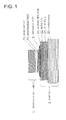
- FIG. 1 The structure of a semiconductor device according to an embodiment of the present invention will now be described with reference to the cross-section view in FIG. 1 .
- the semiconductor element 1/ZnAl solder layer 3/substrate 2 structure shown in FIG. 1 will be referred to as a semiconductor device according to the present example.
- FIGS. 1 and 2 are shown schematically in order to facilitate understanding of the present invention, and the relationship between the thickness and the planar dimensions, the proportion of thicknesses of the layers, and the like may be exaggerated.
- a SiC power element is used as the semiconductor element
- a substrate in which a Cu plate is affixed to both surfaces of a SiN ceramic plate is used as the substrate.
- this is merely an example; a GaN element, a diamond element, a ZnO element, or another wide bandgap semiconductor element, or a Si semiconductor element intended for high-temperature usage (SOI element or sensor element), can be equally employed.
- the substrate is not limited to Cu affixed to an SiN ceramic plate, and may be: a Cu substrate affixed to another type of ceramic substrate; a metal substrate other than Cu (e.g., Al or CuMo) affixed to another type of ceramic substrate (Al 2 O 3 or AIN) or an insulating body; or a simple metal plate made from Cu or a standalone metal other than Cu (without a ceramic or an insulating plate).
- Numeral 1 represents a silicon carbide (SiC) power semiconductor element.
- An ohmic contact 11 is formed on the reverse surface.
- a mounting electrode 12 covers the surface of the ohmic contact 11 in order, e.g., to improve the solder wettability, prevent ingress of the solder, and improve adhesion.
- An example of the mounting electrode 12 is an evaporated Ti/Ni/Ag multilayer film (a layered structure in which the Ti is in contact with the Ohmic contact 11 and Ag represents the outermost surface).
- Numeral 2 represents the substrate.
- the substrate 2 according to the present example has a structure in which a metal plate 21 made from Cu, Al, or another metal is brazed or otherwise affixed on at least one surface of a SiN ceramic plate 20.
- the surface of the metal plate 21 is covered by a metal film 22 comprising N, Pt, Pd, or another metal exhibiting wettability, adhesive properties, and barrier properties with respect to solder.
- a Cu-based metal film 23 having Cu as a principal element and a thickness of 20 nm to 200 nm is formed so as to coat the surface of the metal film 22.
- a ZnAl solder layer 3 is sandwiched between the semiconductor element 1 and the substrate 2.
- the ZnAl solder layer 3 may contain a trace amount (no greater than 1 mass%) of Ge, P, or another element in order to improve the hardness of the solder material, wettability during bonding, and viscosity of the molten liquid.
- the thickness of the ZnAl solder layer 3 is preferably no greater than about 100 ⁇ m, further preferably no greater than 50 ⁇ m, and even further preferably no greater than 30 ⁇ m.
- the structural characteristic of the ZnAl solder layer 3 according to the present example is that although the composition of the ZnAl solder layer 3 according to the present example is eutectic or substantially eutectic, the structure thereof either does not contain a eutectic structure at all or contains an eutectic structure to an extent that does not exceed 20%. This matter will be described further below.
- Precursor material A is a power semiconductor element 1 made from silicon carbide (SiC) shown in FIG. 1 mentioned further above.
- Silicon carbide (SiC) semiconductor elements 1 that are commercially available substantially have, in reality, the structure shown in FIG. 1 . Therefore, as long as a semiconductor element of such description is used, there is no need for a particular modification in order to carry out the present invention.
- Precursor material B is the substrate 2 shown in FIG. 1 mentioned further above.
- the Cu installed on the surface of the substrate 2 has a property of readily forming an alloy with a Zn component in molten ZnAl solder. Therefore, the Cu has an effect of promoting the spread of the molten ZnAl eutectic solder and contributing to the reduction in reflow time, as well as reducing the thickness of the ZnAl solder layer 3 formed.
- the substrate 2 is widely commercially available, and is therefore extremely easy to obtain.
- the dimensions of the ZnAl solder chip 3' are set to be smaller than the dimensions of a die for the semiconductor element 1.
- the thickness of the ZnAl solder chip 3' is preferably no greater than 50 ⁇ m and is further preferably 30 ⁇ m.
- the ZnAl solder chip 3' is exposed to the atmosphere before bonding; therefore, it shall be apparent that a natural oxide film is formed on the surface.
- a semiconductor device can be produced without any problems, even when a ZnAl solder chip 3' of such description is used.
- organic cleaning is performed using a solvent such as acetone or isopropyl alcohol, and contaminants adhering to the surface of the precursor materials are removed.
- the decompression reflow device has an exhaust capacity enabling decompression down to about 5 millibars, and is configured so as to be able to introduce an inert gas (nitrogen or argon gas) having a purity of no less than 99.99%.
- an inert gas nitrogen or argon gas
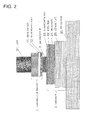
- FIG. 2 is a cross-section view showing the precursor materials A to C placed in a sample compartment (chamber in which a reflow stage 30 is placed) of a decompression reflow device.
- the substrate 2 is placed on the reflow stage 30, the ZnAl solder chip 3' and the semiconductor element 1 with the bonding surface facing downwards are overlapped so as to be aligned with the portion on the substrate 2 to be bonded, and a load member 31 is placed on top thereof.
- the first point is the manner in which the ZnAl solder chip 3' is placed. It is important to place the ZnAl solder chip 3' so that when the ZnAl solder chip 3' and the semiconductor element 1 are overlapped, the ZnAl solder chip 3' does not protrude beyond the outer periphery of the semiconductor element 1.
- the thickness of the resulting ZnAl solder layer 3 can be controlled so as to be small and uniform.
- the second point is to use a static load member 31.
- a gentle pressure is applied to the semiconductor element 1 during solder melting in order to form a satisfactory bond.
- the necessary load is preferably no less than 0.1 g/cm 2 and further preferably no less than 0.3 g/cm 2 .
- the load to be used is preferably no less than 0.4 g and further preferably no less than 1.2 g.
- the thickness of the ZnAl solder layer 3 is further reduced, making it possible to reduce the thickness to 50 ⁇ m or less, such a thickness having a property in which eutectic phase structures do not readily form.
- a reflow step is performed. First, air in the sample compartment of the decompression reflow device is discharged. When the pressure in the sample compartment has fallen to 5 millibar or less, the inert gas is introduced. This operation is performed several times, and the air in the sample compartment is replaced with the inert gas. The sample compartment is thereby filled with the inert gas.
- the reflow stage 30 or the entire sample compartment is heated, the temperature of the precursor materials A to C is increased to about 200°C and maintained for approximately 2 minutes. At this time, an inert gas containing formic acid vapor may be introduced and removal of contaminant organic matter promoted.
- the introduction of the inert gas is discontinued, gas discharging is restarted, and the pressure in the sample compartment is reduced to 5 millibar or less; at the same time, the reflow stage 30 or the entire sample compartment is further heated, and the temperature of the precursor materials A to C is increased to and maintained at a predetermined temperature defined within a temperature range ranging from the liquidus temperature of the ZnAl solder chip 3' to 420°C.
- a holding time of as much as 5 minutes will be adequate.
- a typical holding time when the predetermined temperature is 415°C is 1 minute.
- the melting point (382°C) is exceeded, the ZnAl solder chip 3' is turned into a molten liquid, flattened by the load from the load member 31, and caused to radially spread on the substrate 2 surrounding the semiconductor element 1.
- the inert gas is introduced into the sample compartment.
- a reduction in the temperature of the reflow stage 30 or the entire sample compartment is immediately commenced.
- annealing is performed for several minutes to several tens of minutes while the temperature is temporarily maintained or reduced at a gradual pace. This annealing step acts effectively to convert ZnAl eutectic phase structures, which are harmful and thermally unstable, contained in the ZnAl solder layer 3 into ZnAl eutectoid phase structures and Zn phase structures.
- the annealing step has an effect of eliminating eutectic phase structures which are generated when the molten ZnAl eutectic solder liquid is caused to rapidly solidify.
- a load member 31 of less than 0.3 g/cm 2 is used during the reflow, this conversion occurs over an extremely short period of time, and the annealing step can therefore be omitted.
- the reflow stage 30 or the entire sample compartment is cooled to room temperature, completing the semiconductor device of the present example.
- a high concentration of ZnAl eutectic phase structures are normally formed.
- SEM cross-section scanning electron micrograph
- countless microcracks are formed at the interfaces between the eutectic phase structures (regions resembling stripes on pearl oyster shells) and other structures, i.e., between Zn phase structures (regions having a white uniform contrast) and ZnAl eutectoid phase structures (regions containing scattered small black-contrast dots).
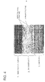
- FIG. 4 is a cross-sectional scanning electron micrograph of the ZnAl solder layer 3 in a silicon carbide semiconductor element 1/ZnAl solder layer 3/substrate 2 structure produced according to the abovementioned manufacturing method according to the present example.
- the ZnAl solder layer 3 in the sample shown comprises only Zn phase structures and ZnAl eutectoid phase structures, and that eutectic phase structures are not contained at all.
- This micrograph is a typical cross-sectional scanning electron micrograph of a sample in which the thickness of the ZnAl solder layer 3 is no greater than 50 ⁇ m. However, it was established that a sample in which the thickness of the ZnAl solder layer 3 is greater than 50 ⁇ m has basically the same cross-sectional structure as that in this micrograph (other than the thickness of the ZnAl solder layer 3 being greater).
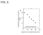
- FIG. 5 is a graph obtained by measuring the bonding strength at different test temperatures along the horizontal axis from room temperature to 300°C and plotting the average values of the obtained bonding strengths against the test temperature.
- the bonding strength (average value) at room temperature is approximately 120 MPa. This is an extremely satisfactory value equivalent to approximately 20 times that according to the international standard (IEC60749-19) defined in relation to the bonding strength of semiconductor devices.
- IEC60749-19 the bonding strength
- the extent by which the semiconductor device degrades during a soldering treatment lasting a short period of time as described above is negligible.
- the solder layer 3 comprises a well-known, simple ZnAl eutectic solder
- the cost of manufacturing the solder material is prevented from increasing.
- the bonding step according to the present example is not sensitive to the oxygen concentration in the atmosphere, and can be readily achieved using a gas and a generic decompression reflow device commonly used in PbSn soldering. As a result, there is no need for a dedicated reflow device such as a sophisticated reflow device equipped with a substrate heating means provided with an explosion-proof function and the like.
- the thickness of the ZnAl solder layer 3 is set to preferably no greater than 50 ⁇ m and further preferably no greater than 30 ⁇ m, whereby the ZnAl solder layer 3 is formed so as to be extremely thin, resulting in the effect of it being possible to reduce the thermal resistance, against thermal conduction, of the ZnAl solder layer 3.
- employing a substrate 2 in which the principal element, at least at the surface, is Cu has an effect of promoting the spread of the molten ZnAl eutectic solder and contributing to reducing the reflow time, as well as reducing the thickness of the ZnAl solder layer 3 formed.
- a ZnAl solder chip 3' having a smaller shape than that of the semiconductor element 1 is used, and caused to melt while being subjected to a static load; therefore, the Zn or Al natural oxide film coating covering the molten ZnAl solder liquid pulverizes instantaneously, making it possible to cause a bonding reaction between the molten liquid and the substrate 2 and between the molten liquid and the semiconductor element 1 in a swift and reproducible manner.
- the thickness of the resulting ZnAl solder layer 3 can be controlled so as to be small and uniform.
- the ZnAl solder chip 3' having a ZnAl eutectic or substantially eutectic composition is increased in temperature while being subjected to a load, caused to melt, and subsequently reduced in temperature, whereby the ZnAl eutectic phase structure changes to a ZnAl eutectoid phase structure, and the ZnAl solder layer becomes a structure having a small number of ZnAl eutectic phases and a large number of Zn phases and ZnAl eutectoid phases.
- the stress difference at phase interfaces is thereby minimized, and as a result, the variation in bonding strength is minimized and the yield of the obtained product is improved.
- the temperature is maintained or reduced at a gradual pace at a temperature immediately below the eutectoid temperature of the ZnAl solder layer during the reduction in temperature, which acts to effectively convert ZnAl eutectic phase structures, which are harmful and thermally unstable, contained in the ZnAl solder layer 3 into ZnAl eutectoid phase structures and Zn phase structures.
- having the static load be no less than 0.1 g/mm 2 and preferably no less than 0.3 g/mm 2 further reduces the thickness of the ZnAl solder layer 3, making it possible to reduce the thickness to 50 ⁇ m or less, such a thickness having a property in which eutectic phase structures do not readily form.
Landscapes
- Engineering & Computer Science (AREA)
- Mechanical Engineering (AREA)
- Chemical & Material Sciences (AREA)
- Materials Engineering (AREA)
- Metallurgy (AREA)
- Organic Chemistry (AREA)
- Die Bonding (AREA)
Abstract
Description
- The present invention relates to a method for manufacturing a semiconductor device in which a semiconductor element and a substrate are bonded using a zinc-aluminum based bonding material, and to a semiconductor device thereby obtained.
- Wide bandgap semiconductors such as silicon carbide (SiC) and gallium nitride (GaN) are capable of handling large currents at a high actuation voltage, and a high heat resistance is therefore required from portions that are bonded by soldering. Therefore, there has been proposed a zinc-aluminum-based ZnAl eutectic solder as a material for bonding high-temperature actuation devices such as power semiconductor devices (Patent Citation 1).
- Patent Citation 1:
JP-A 2009-125753 - However, when the inventors in the present application attempted to bond a power semiconductor element and a substrate using the bonding method disclosed in the above Patent Citation 1, it was found that the bonding strength varied significantly.
- An object of the present invention is to minimize variation in the strength of bonding between a semiconductor element and a substrate, and to improve the yield of the obtained product.
- In the present invention, ZnAl eutectic solder sandwiched between a semiconductor element and a substrate having Cu as a principal element on the surface is increased in temperature while being subjected to a load, caused to melt, and subsequently reduced in temperature while being subjected to a load, whereby the above object is achieved.
- According to the present invention, ZnAl eutectic phase structures change to ZnAl eutectoid phase structures, and the ZnAl solder layer becomes a structure having a small number of ZnAl eutectic phases and a large number of Zn phases and ZnAl eutectoid phases. The stress difference at the phase interfaces is thereby minimized; as a result, the variation in bonding strength is minimised and the yield of the obtained product is improved.
-
-
FIG. 1 is a cross-section view showing a semiconductor device according to an embodiment of the present invention; -
FIG. 2 is a cross-section view for illustrating a method for manufacturing the semiconductor device inFIG. 1 ; -
FIG. 3 is a scanning electron micrograph of a cross-section of the semiconductor device produced according to the method disclosed in Patent Citation 1; -
FIG. 4 is a scanning electron micrograph of a cross-section of a semiconductor device produced according to the method for manufacturing a semiconductor device inFIG. 2 ; and -
FIG. 5 is a graph showing temperature characteristics of the shear strength of the semiconductor device produced according to the method for manufacturing a semiconductor device inFIG. 2 . - The structure of a semiconductor device according to an embodiment of the present invention will now be described with reference to the cross-section view in
FIG. 1 . Thesemiconductor element 1/ZnAl solder layer 3/substrate 2 structure shown inFIG. 1 will be referred to as a semiconductor device according to the present example.FIGS. 1 and2 are shown schematically in order to facilitate understanding of the present invention, and the relationship between the thickness and the planar dimensions, the proportion of thicknesses of the layers, and the like may be exaggerated. - In the following description, the present invention will be described in detail using an example in which a SiC power element is used as the semiconductor element, and a substrate in which a Cu plate is affixed to both surfaces of a SiN ceramic plate is used as the substrate. However, this is merely an example; a GaN element, a diamond element, a ZnO element, or another wide bandgap semiconductor element, or a Si semiconductor element intended for high-temperature usage (SOI element or sensor element), can be equally employed. The substrate is not limited to Cu affixed to an SiN ceramic plate, and may be: a Cu substrate affixed to another type of ceramic substrate; a metal substrate other than Cu (e.g., Al or CuMo) affixed to another type of ceramic substrate (Al2O3 or AIN) or an insulating body; or a simple metal plate made from Cu or a standalone metal other than Cu (without a ceramic or an insulating plate).
-
Numeral 1 represents a silicon carbide (SiC) power semiconductor element. Anohmic contact 11 is formed on the reverse surface. Amounting electrode 12 covers the surface of theohmic contact 11 in order, e.g., to improve the solder wettability, prevent ingress of the solder, and improve adhesion. An example of themounting electrode 12 is an evaporated Ti/Ni/Ag multilayer film (a layered structure in which the Ti is in contact with theOhmic contact 11 and Ag represents the outermost surface). -
Numeral 2 represents the substrate. Thesubstrate 2 according to the present example has a structure in which a metal plate 21 made from Cu, Al, or another metal is brazed or otherwise affixed on at least one surface of a SiN ceramic plate 20. The surface of the metal plate 21 is covered by a metal film 22 comprising N, Pt, Pd, or another metal exhibiting wettability, adhesive properties, and barrier properties with respect to solder. In addition, a Cu-basedmetal film 23 having Cu as a principal element and a thickness of 20 nm to 200 nm is formed so as to coat the surface of the metal film 22. - A
ZnAl solder layer 3 is sandwiched between thesemiconductor element 1 and thesubstrate 2. The composition of Zn and Al in theZnAl solder layer 3 in the present example is preferably eutectic (Al concentration = 5 mass%) or substantially eutectic (Al concentration within 5 ± 2 mass%). In addition, theZnAl solder layer 3 may contain a trace amount (no greater than 1 mass%) of Ge, P, or another element in order to improve the hardness of the solder material, wettability during bonding, and viscosity of the molten liquid. In the semiconductor device of the present invention, no particular limitation exists with regards to the thickness of theZnAl solder layer 3. However, in practical use, the thickness of theZnAl solder layer 3 is preferably no greater than about 100 µm, further preferably no greater than 50 µm, and even further preferably no greater than 30 µm. - The structural characteristic of the
ZnAl solder layer 3 according to the present example is that although the composition of theZnAl solder layer 3 according to the present example is eutectic or substantially eutectic, the structure thereof either does not contain a eutectic structure at all or contains an eutectic structure to an extent that does not exceed 20%. This matter will be described further below. - Next, a description will be given for a method for manufacturing a semiconductor device having the above structure. First, precursor materials A to C having the following specifications are readied.
- Precursor material A is a
power semiconductor element 1 made from silicon carbide (SiC) shown inFIG. 1 mentioned further above. Silicon carbide (SiC)semiconductor elements 1 that are commercially available substantially have, in reality, the structure shown inFIG. 1 . Therefore, as long as a semiconductor element of such description is used, there is no need for a particular modification in order to carry out the present invention. - Precursor material B is the
substrate 2 shown inFIG. 1 mentioned further above. The Cu installed on the surface of thesubstrate 2 has a property of readily forming an alloy with a Zn component in molten ZnAl solder. Therefore, the Cu has an effect of promoting the spread of the molten ZnAl eutectic solder and contributing to the reduction in reflow time, as well as reducing the thickness of theZnAl solder layer 3 formed. Thesubstrate 2 is widely commercially available, and is therefore extremely easy to obtain. - Precursor material C is a chip-shaped ZnAl solder chip 3' prepared so as to have an eutectic composition (Al concentration = 5 mass%) or a substantially eutectic composition (Al concentration within 5 ± 2 mass%). The dimensions of the ZnAl solder chip 3' are set to be smaller than the dimensions of a die for the
semiconductor element 1. In the present example, the thickness of the ZnAl solder chip 3' is preferably no greater than 50 µm and is further preferably 30 µm. The ZnAl solder chip 3' is exposed to the atmosphere before bonding; therefore, it shall be apparent that a natural oxide film is formed on the surface. However, in the present example, a semiconductor device can be produced without any problems, even when a ZnAl solder chip 3' of such description is used. - When the precursor materials A to C are ready, organic cleaning is performed using a solvent such as acetone or isopropyl alcohol, and contaminants adhering to the surface of the precursor materials are removed.
- Next, the precursor materials A to C are installed in a decompression reflow device. The decompression reflow device has an exhaust capacity enabling decompression down to about 5 millibars, and is configured so as to be able to introduce an inert gas (nitrogen or argon gas) having a purity of no less than 99.99%.
-
FIG. 2 is a cross-section view showing the precursor materials A to C placed in a sample compartment (chamber in which areflow stage 30 is placed) of a decompression reflow device. As shown in the drawing, thesubstrate 2 is placed on thereflow stage 30, the ZnAl solder chip 3' and thesemiconductor element 1 with the bonding surface facing downwards are overlapped so as to be aligned with the portion on thesubstrate 2 to be bonded, and aload member 31 is placed on top thereof. - There are important points with regards to the above in relation to the manufacture of a semiconductor device according to the present example. The first point is the manner in which the ZnAl solder chip 3' is placed. It is important to place the ZnAl solder chip 3' so that when the ZnAl solder chip 3' and the
semiconductor element 1 are overlapped, the ZnAl solder chip 3' does not protrude beyond the outer periphery of thesemiconductor element 1. Having the dimensions of the ZnAl solder chip 3' so as to be smaller than those of thesemiconductor element 1, placing the ZnAl solder chip 3' so as to not protrude beyond the outer periphery of thesemiconductor element 1, and causing the ZnAl solder chip 3' to melt while applying a load, cause the Zn or Al natural oxide film coating covering the molten ZnAl solder liquid to pulverize instantaneously, and make it possible to cause a bonding reaction between the molten liquid and thesubstrate 2 and between the molten liquid and thesemiconductor element 1 in a swift and reproducible manner. In addition, the thickness of the resultingZnAl solder layer 3 can be controlled so as to be small and uniform. - The second point is to use a
static load member 31. In the present example, a gentle pressure is applied to thesemiconductor element 1 during solder melting in order to form a satisfactory bond. The necessary load is preferably no less than 0.1 g/cm2 and further preferably no less than 0.3 g/cm2. For example, for asemiconductor element 1 measuring 4 mm2, the load to be used is preferably no less than 0.4 g and further preferably no less than 1.2 g. In particular, if a load of no less than 0.3 g/cm2 is employed, the thickness of theZnAl solder layer 3 is further reduced, making it possible to reduce the thickness to 50 µm or less, such a thickness having a property in which eutectic phase structures do not readily form. - When the above preparations are done, a reflow step is performed. First, air in the sample compartment of the decompression reflow device is discharged. When the pressure in the sample compartment has fallen to 5 millibar or less, the inert gas is introduced. This operation is performed several times, and the air in the sample compartment is replaced with the inert gas. The sample compartment is thereby filled with the inert gas.
- Then, the
reflow stage 30 or the entire sample compartment is heated, the temperature of the precursor materials A to C is increased to about 200°C and maintained for approximately 2 minutes. At this time, an inert gas containing formic acid vapor may be introduced and removal of contaminant organic matter promoted. - Next, the introduction of the inert gas is discontinued, gas discharging is restarted, and the pressure in the sample compartment is reduced to 5 millibar or less; at the same time, the
reflow stage 30 or the entire sample compartment is further heated, and the temperature of the precursor materials A to C is increased to and maintained at a predetermined temperature defined within a temperature range ranging from the liquidus temperature of the ZnAl solder chip 3' to 420°C. A holding time of as much as 5 minutes will be adequate. A typical holding time when the predetermined temperature is 415°C is 1 minute. When the melting point (382°C) is exceeded, the ZnAl solder chip 3' is turned into a molten liquid, flattened by the load from theload member 31, and caused to radially spread on thesubstrate 2 surrounding thesemiconductor element 1. - Next, the inert gas is introduced into the sample compartment. When the pressure has increased to a predetermined pressure, a reduction in the temperature of the
reflow stage 30 or the entire sample compartment is immediately commenced. In this instance, it is preferable that when the temperature has fallen below 275°C, which is the eutectoid temperature of the ZnAl alloy, annealing is performed for several minutes to several tens of minutes while the temperature is temporarily maintained or reduced at a gradual pace. This annealing step acts effectively to convert ZnAl eutectic phase structures, which are harmful and thermally unstable, contained in theZnAl solder layer 3 into ZnAl eutectoid phase structures and Zn phase structures. In other words, the annealing step has an effect of eliminating eutectic phase structures which are generated when the molten ZnAl eutectic solder liquid is caused to rapidly solidify. However, if aload member 31 of less than 0.3 g/cm2 is used during the reflow, this conversion occurs over an extremely short period of time, and the annealing step can therefore be omitted. - Then, the
reflow stage 30 or the entire sample compartment is cooled to room temperature, completing the semiconductor device of the present example. - In a semiconductor device in which a ZnAl eutectic solder disclosed in
Patent Citation 1 is used, there is significant variation in bonding strength, and it is difficult to manufacture a product that is suitable for practical use. As a result of examining in detail a large number of defective samples of such description, the inventors in the present application arrived at the following explanation for the abovementioned problems. - Specifically, in a
ZnAl solder layer 3 of asemiconductor element 1/ZnAl solder layer 3/substrate 2 structure in which a ZnAl solder chip 3' is used, a high concentration of ZnAl eutectic phase structures are normally formed. As shown in the cross-section scanning electron micrograph (SEM) inFIG. 3 , countless microcracks are formed at the interfaces between the eutectic phase structures (regions resembling stripes on pearl oyster shells) and other structures, i.e., between Zn phase structures (regions having a white uniform contrast) and ZnAl eutectoid phase structures (regions containing scattered small black-contrast dots). - When the proportion of eutectic phase structures contained exceeds 20%, the microcracks rapidly join, readily forming large cracks at the interface of the eutectic phase structures, resulting in a significant decrease in bonding strength. It is presumed that the variation in the manner in which such cracks occur result in the variation in bonding strength. It is thought that normally the presence of a plurality of structures causes stress differences to occur at the interfaces of the structures, generating microcracks as a result.
- In response, the inventors, with an idea to reduce the formation of ZnAl eutectic phase structures to 20% or less, searched for a manufacturing method that can be implemented, and succeeded in actually forming a structure of such description using the abovementioned manufacturing method and established that a semiconductor device having sufficient bonding strength can be manufactured by adopting the abovementioned structure.
FIG. 4 is a cross-sectional scanning electron micrograph of theZnAl solder layer 3 in a siliconcarbide semiconductor element 1/ZnAl solder layer 3/substrate 2 structure produced according to the abovementioned manufacturing method according to the present example. - It can be seen that the
ZnAl solder layer 3 in the sample shown comprises only Zn phase structures and ZnAl eutectoid phase structures, and that eutectic phase structures are not contained at all. This micrograph is a typical cross-sectional scanning electron micrograph of a sample in which the thickness of theZnAl solder layer 3 is no greater than 50 µm. However, it was established that a sample in which the thickness of theZnAl solder layer 3 is greater than 50 µm has basically the same cross-sectional structure as that in this micrograph (other than the thickness of theZnAl solder layer 3 being greater). - In addition, the bonding strength of a semiconductor device having a silicon
carbide semiconductor element 1/ZnAl solder layer 3/substrate 2 structure of the present example was evaluated by die shear testing. The size of the siliconcarbide semiconductor element 1 in this instance was 2 × 2 mm2.FIG. 5 is a graph obtained by measuring the bonding strength at different test temperatures along the horizontal axis from room temperature to 300°C and plotting the average values of the obtained bonding strengths against the test temperature. - As can be seen from
FIG. 5 , the bonding strength (average value) at room temperature is approximately 120 MPa. This is an extremely satisfactory value equivalent to approximately 20 times that according to the international standard (IEC60749-19) defined in relation to the bonding strength of semiconductor devices. In addition, as can be seen fromFIG. 5 , although the bonding strength gradually falls with increasing test temperature, it was established that even at 300°C, the bonding strength is still approximately 7 times that according to the standard. - As described above, the
solder layer 3 of the semiconductor device according to the present example comprises ZnAl eutectic solder; therefore, the melting point thereof (= liquidus temperature = solidus temperature = eutectic temp) is low, in the vicinity of 382°C, and as a result, the semiconductor device can be manufactured through a soldering treatment lasting 5 minutes or less at a temperature no greater than 420°C. The extent by which the semiconductor device degrades during a soldering treatment lasting a short period of time as described above is negligible. Specifically, according to the present example, it is possible to minimize problems of the semiconductor device failing to withstand the heat during soldering and becoming defective. - In addition, since the
solder layer 3 comprises a well-known, simple ZnAl eutectic solder, there is no need to perform a process of adding a special film, and the cost of manufacturing the solder material is prevented from increasing. Specifically, according to the present example, there is no need to produce a special ZnAl solder material coated with an easily reducible metal (Cu, Ag, Au), and the manufacturing cost of the ZnAl solder is kept low. - In addition, according to the present example, as shown in
FIG. 5 , it is possible to manufacture a semiconductor device having a sufficient bonding strength. In particular, the bonding step according to the present example is not sensitive to the oxygen concentration in the atmosphere, and can be readily achieved using a gas and a generic decompression reflow device commonly used in PbSn soldering. As a result, there is no need for a dedicated reflow device such as a sophisticated reflow device equipped with a substrate heating means provided with an explosion-proof function and the like. - According to the present example, the thickness of the
ZnAl solder layer 3 is set to preferably no greater than 50 µm and further preferably no greater than 30 µm, whereby theZnAl solder layer 3 is formed so as to be extremely thin, resulting in the effect of it being possible to reduce the thermal resistance, against thermal conduction, of theZnAl solder layer 3. - In the present example, employing a
substrate 2 in which the principal element, at least at the surface, is Cu has an effect of promoting the spread of the molten ZnAl eutectic solder and contributing to reducing the reflow time, as well as reducing the thickness of theZnAl solder layer 3 formed. - In the present example, a ZnAl solder chip 3' having a smaller shape than that of the
semiconductor element 1 is used, and caused to melt while being subjected to a static load; therefore, the Zn or Al natural oxide film coating covering the molten ZnAl solder liquid pulverizes instantaneously, making it possible to cause a bonding reaction between the molten liquid and thesubstrate 2 and between the molten liquid and thesemiconductor element 1 in a swift and reproducible manner. In addition, the thickness of the resultingZnAl solder layer 3 can be controlled so as to be small and uniform. In particular, installing the ZnAl solder chip 3' having a smaller shape than that of thesemiconductor element 1 so as to not protrude beyond the outer periphery of thesemiconductor element 1 results in the pulverization of the natural oxide film coating being aided in a uniform manner, further enhancing the abovementioned effect. - Also, in the present example, the ZnAl solder chip 3' having a ZnAl eutectic or substantially eutectic composition is increased in temperature while being subjected to a load, caused to melt, and subsequently reduced in temperature, whereby the ZnAl eutectic phase structure changes to a ZnAl eutectoid phase structure, and the ZnAl solder layer becomes a structure having a small number of ZnAl eutectic phases and a large number of Zn phases and ZnAl eutectoid phases. The stress difference at phase interfaces is thereby minimized, and as a result, the variation in bonding strength is minimized and the yield of the obtained product is improved.
- According to the present example, the temperature is maintained or reduced at a gradual pace at a temperature immediately below the eutectoid temperature of the ZnAl solder layer during the reduction in temperature, which acts to effectively convert ZnAl eutectic phase structures, which are harmful and thermally unstable, contained in the
ZnAl solder layer 3 into ZnAl eutectoid phase structures and Zn phase structures. - In the present example, having the static load be no less than 0.1 g/mm2 and preferably no less than 0.3 g/mm2 further reduces the thickness of the
ZnAl solder layer 3, making it possible to reduce the thickness to 50 µm or less, such a thickness having a property in which eutectic phase structures do not readily form. -
- 1
- Silicon carbide semiconductor device
- 2
- Metal substrate
- 3
- ZnAl solder layer
- 11
- Ohmic contact
- 12
- Mounting electrode
- 20
- Ceramic plate
- 21
- Metal plate
- 22
- Metal film
- 23
- Cu-based metal film
- 3'
- ZnAl solder chip
- 30
- Reflow stage
- 31
- Load
Claims (7)
- A method for manufacturing a semiconductor device, comprising:a step for readying each of a semiconductor element, a substrate having Cu as a principal element at least on a surface, and a ZnAl eutectic solder chip having a smaller shape than that of the semiconductor element;a step for disposing the semiconductor element and the substrate so that respective bonding surfaces face each other, and sandwiching the ZnAl eutectic solder chip between the substrate and the semiconductor element;a step for increasing the temperature of the ZnAl solder chip sandwiched between the substrate and the semiconductor element while applying a load to the ZnAl solder chip, causing the ZnAl solder chip to melt, and forming a ZnAl solder layer; anda step for reducing the temperature of the ZnAl solder layer while applying a load to the ZnAl solder layer.
- The method for manufacturing a semiconductor device according to claim 1, wherein the step for reducing the temperature includes a step for maintaining the temperature, or reducing the temperature at a gradual pace, immediately below the eutectoid temperature of the ZnAl solder layer.
- The method for manufacturing a semiconductor device according to claim 1 or 2, wherein the load is no less than 0.1 g/mm2.
- The method for manufacturing a semiconductor device according to any of claims 1-3, wherein a maximum melting temperature of the ZnAl eutectic solder chip is no less than the liquidus temperature of the ZnAl eutectic solder chip and no greater than 420°C.
- The method for manufacturing a semiconductor device according to claim 4, wherein the temperature is held at the maximum melting temperature for 5 minutes or less.
- A semiconductor device in which a ZnAl solder layer is sandwiched between a semiconductor element and a substrate, wherein the eutectic phase structure content relative to the entire ZnAl solder layer is no greater than 20%.
- The semiconductor device disclosed in claim 6, wherein the semiconductor element has, as a base body, a wide bandgap semiconductor containing silicon carbide (SiC), gallium nitride (GaN), and diamond (C).
Applications Claiming Priority (2)
| Application Number | Priority Date | Filing Date | Title |
|---|---|---|---|
| JP2011165508A JP5675525B2 (en) | 2011-07-28 | 2011-07-28 | Semiconductor device manufacturing method and semiconductor device |
| PCT/JP2012/069096 WO2013015402A1 (en) | 2011-07-28 | 2012-07-27 | Method for manufacturing semiconductor device, and semiconductor device |
Publications (3)
| Publication Number | Publication Date |
|---|---|
| EP2738794A1 true EP2738794A1 (en) | 2014-06-04 |
| EP2738794A4 EP2738794A4 (en) | 2015-11-04 |
| EP2738794B1 EP2738794B1 (en) | 2018-09-12 |
Family
ID=47601233
Family Applications (1)
| Application Number | Title | Priority Date | Filing Date |
|---|---|---|---|
| EP12818068.4A Not-in-force EP2738794B1 (en) | 2011-07-28 | 2012-07-27 | Method for manufacturing semiconductor device, and semiconductor device |
Country Status (4)
| Country | Link |
|---|---|
| US (1) | US8975182B2 (en) |
| EP (1) | EP2738794B1 (en) |
| JP (1) | JP5675525B2 (en) |
| WO (1) | WO2013015402A1 (en) |
Cited By (1)
| Publication number | Priority date | Publication date | Assignee | Title |
|---|---|---|---|---|
| CN105965120A (en) * | 2016-06-03 | 2016-09-28 | 湖北三江航天险峰电子信息有限公司 | Semi-automatic eutectic soldering method of GaAs microwave power amplifier chip and product |
Families Citing this family (9)
| Publication number | Priority date | Publication date | Assignee | Title |
|---|---|---|---|---|
| JP6069135B2 (en) * | 2013-08-30 | 2017-02-01 | 株式会社日立製作所 | Power semiconductor device, method of manufacturing the same, and solder for the same |
| TWI561639B (en) * | 2014-04-17 | 2016-12-11 | Heraeus Materials Singapore Pte Ltd | Lead-free eutectic solder alloy comprising zinc as the main component and aluminum as an alloying metal |
| JP2016098165A (en) * | 2014-11-26 | 2016-05-30 | 株式会社テリーサ研究所 | Soldering method for jointing solder to ceramic |
| JP6354954B2 (en) * | 2015-05-15 | 2018-07-11 | トヨタ自動車株式会社 | Semiconductor device manufacturing method and semiconductor device |
| JP6590336B2 (en) * | 2015-06-03 | 2019-10-16 | 国立大学法人茨城大学 | High heat-resistant solder junction semiconductor device and manufacturing method thereof |
| JP6493161B2 (en) * | 2015-11-05 | 2019-04-03 | トヨタ自動車株式会社 | Manufacturing method of semiconductor device |
| US10879211B2 (en) | 2016-06-30 | 2020-12-29 | R.S.M. Electron Power, Inc. | Method of joining a surface-mount component to a substrate with solder that has been temporarily secured |
| EP3616827B1 (en) | 2017-04-28 | 2024-03-20 | Mitsubishi Electric Corporation | Junction structure, method for manufacturing same, electric motor, and method for manufacturing same |
| CN109873068B (en) * | 2019-01-08 | 2024-03-15 | 王耀村 | Eutectic machine |
Family Cites Families (10)
| Publication number | Priority date | Publication date | Assignee | Title |
|---|---|---|---|---|
| JPS6316628A (en) * | 1986-07-08 | 1988-01-23 | Mitsubishi Electric Corp | Semiconductor device |
| JPH10140307A (en) * | 1996-11-08 | 1998-05-26 | Suzuki Motor Corp | Heat treatment method for Zn alloy |
| JP2001093916A (en) * | 1999-09-24 | 2001-04-06 | Toshiba Corp | Semiconductor device and manufacturing method thereof |
| ES2228816T3 (en) * | 2000-01-28 | 2005-04-16 | Gea Energietechnik Gmbh | PROCEDURE FOR THE UNION OF STEEL PIPES WITH ALUMINUM NERVES. |
| JP2002203932A (en) * | 2000-10-31 | 2002-07-19 | Hitachi Ltd | Heat dissipation board for semiconductor power element, its conductor plate, heat sink material and solder material |
| JP4772320B2 (en) * | 2004-12-15 | 2011-09-14 | 富士通株式会社 | Zinc-aluminum solder alloy |
| JP4390799B2 (en) * | 2006-11-21 | 2009-12-24 | 株式会社日立製作所 | Connection material, method for manufacturing connection material, and semiconductor device |
| US20080136019A1 (en) * | 2006-12-11 | 2008-06-12 | Johnson Michael E | Solder Bump/Under Bump Metallurgy Structure for High Temperature Applications |
| JP4803834B2 (en) * | 2007-11-02 | 2011-10-26 | 国立大学法人茨城大学 | Zn-Al eutectoid alloy bonding material, method for producing Zn-Al eutectoid alloy bonding material, bonding method using Zn-Al eutectoid alloy bonding material, and Zn-Al eutectoid alloy bonding material Semiconductor device |
| JP5160201B2 (en) * | 2007-11-20 | 2013-03-13 | 株式会社豊田中央研究所 | Solder material and manufacturing method thereof, joined body and manufacturing method thereof, power semiconductor module and manufacturing method thereof |
-
2011
- 2011-07-28 JP JP2011165508A patent/JP5675525B2/en not_active Expired - Fee Related
-
2012
- 2012-07-27 EP EP12818068.4A patent/EP2738794B1/en not_active Not-in-force
- 2012-07-27 WO PCT/JP2012/069096 patent/WO2013015402A1/en not_active Ceased
- 2012-07-27 US US14/234,476 patent/US8975182B2/en active Active
Cited By (1)
| Publication number | Priority date | Publication date | Assignee | Title |
|---|---|---|---|---|
| CN105965120A (en) * | 2016-06-03 | 2016-09-28 | 湖北三江航天险峰电子信息有限公司 | Semi-automatic eutectic soldering method of GaAs microwave power amplifier chip and product |
Also Published As
| Publication number | Publication date |
|---|---|
| CN103733321A (en) | 2014-04-16 |
| US20140191250A1 (en) | 2014-07-10 |
| WO2013015402A1 (en) | 2013-01-31 |
| US8975182B2 (en) | 2015-03-10 |
| JP2013030607A (en) | 2013-02-07 |
| EP2738794A4 (en) | 2015-11-04 |
| JP5675525B2 (en) | 2015-02-25 |
| EP2738794B1 (en) | 2018-09-12 |
Similar Documents
| Publication | Publication Date | Title |
|---|---|---|
| EP2738794B1 (en) | Method for manufacturing semiconductor device, and semiconductor device | |
| KR101867625B1 (en) | Member for semiconductor manufacturing device | |
| EP3358614B1 (en) | Circuit substrate and semiconductor device | |
| EP2579696B1 (en) | Circuit board and electronic device using the same | |
| US10727167B2 (en) | Power semiconductor device and method for manufacturing power semiconductor device | |
| JP3949459B2 (en) | Joined body of different materials and manufacturing method thereof | |
| JPWO2002078085A1 (en) | Electronic component package and method of manufacturing the same | |
| US9698082B2 (en) | Au-based solder die attachment semiconductor device and method for manufacturing the same | |
| Bajwa et al. | Foil based transient liquid phase bonding as a die-attachment method for high temperature devices | |
| Shen et al. | Characterization of Bi–Ag–X solder for high temperature SiC die attach | |
| Yu et al. | Pressureless, low temperature sintering of micro-scale silver paste for die attach for 300 C applications | |
| Hagler et al. | SiC Die Attach Metallurgy and Processes for Applications up to 500$^{\circ}{\rm C} $ | |
| JPH0777989B2 (en) | Method for manufacturing ceramic-metal bonded body | |
| JP2015072959A (en) | Bonding structure of insulating substrate and cooler, manufacturing method thereof, power semiconductor module, and manufacturing method thereof | |
| EP3056303B1 (en) | Method for bonding metal bodies and bonding structure for metal bodies | |
| JP6221590B2 (en) | Bonding structure of insulating substrate and cooler, manufacturing method thereof, power semiconductor module, and manufacturing method thereof | |
| JP3794454B2 (en) | Nitride ceramic substrate | |
| CN103733321B (en) | The manufacture method of semiconductor device and semiconductor device | |
| JP6116857B2 (en) | Au-based solder die attachment semiconductor device and manufacturing method thereof | |
| JP6289756B1 (en) | Semiconductor device and manufacturing method thereof | |
| JP3872379B2 (en) | Package for housing semiconductor element and manufacturing method thereof | |
| Wu et al. | High temperature Ag-In joints between Si chips and aluminum | |
| Du et al. | Exploration of a new wafer-level hermetic sealing method by Cu/Sn isothermal solidification technique for MEMS/NEMS devices | |
| JP2026007364A (en) | Vertical nitride semiconductor device manufacturing method and vertical nitride semiconductor device | |
| JP2002037679A (en) | Composite component comprising diferent elements joined together and manufacturing method of the composite component |
Legal Events
| Date | Code | Title | Description |
|---|---|---|---|
| PUAI | Public reference made under article 153(3) epc to a published international application that has entered the european phase |
Free format text: ORIGINAL CODE: 0009012 |
|
| 17P | Request for examination filed |
Effective date: 20140224 |
|
| AK | Designated contracting states |
Kind code of ref document: A1 Designated state(s): AL AT BE BG CH CY CZ DE DK EE ES FI FR GB GR HR HU IE IS IT LI LT LU LV MC MK MT NL NO PL PT RO RS SE SI SK SM TR |
|
| RIN1 | Information on inventor provided before grant (corrected) |
Inventor name: ZUSHI, YUSUKE Inventor name: MURAKAMI, YOSHINORI Inventor name: MATSUI, KOHEI Inventor name: TANIMOTO, SATOSHI Inventor name: TAKAMORI, MASATO Inventor name: ISEKI, TAKASHI |
|
| RAP1 | Party data changed (applicant data changed or rights of an application transferred) |
Owner name: SANKEN ELECTRIC CO., LTD. Owner name: FUJI ELECTRIC CO., LTD. Owner name: SUMITOMO METAL MINING CO., LTD. Owner name: NISSAN MOTOR COMPANY, LIMITED |
|
| RAP1 | Party data changed (applicant data changed or rights of an application transferred) |
Owner name: FUJI ELECTRIC CO., LTD. Owner name: SUMITOMO METAL MINING CO., LTD. Owner name: NISSAN MOTOR CO., LTD. |
|
| DAX | Request for extension of the european patent (deleted) | ||
| RA4 | Supplementary search report drawn up and despatched (corrected) |
Effective date: 20151005 |
|
| RIC1 | Information provided on ipc code assigned before grant |
Ipc: C22C 18/04 20060101ALI20150929BHEP Ipc: H01L 21/52 20060101AFI20150929BHEP Ipc: B23K 1/008 20060101ALI20150929BHEP Ipc: B23K 1/19 20060101ALI20150929BHEP Ipc: B23K 1/20 20060101ALI20150929BHEP Ipc: B23K 35/28 20060101ALI20150929BHEP |
|
| STAA | Information on the status of an ep patent application or granted ep patent |
Free format text: STATUS: EXAMINATION IS IN PROGRESS |
|
| 17Q | First examination report despatched |
Effective date: 20171020 |
|
| GRAP | Despatch of communication of intention to grant a patent |
Free format text: ORIGINAL CODE: EPIDOSNIGR1 |
|
| STAA | Information on the status of an ep patent application or granted ep patent |
Free format text: STATUS: GRANT OF PATENT IS INTENDED |
|
| INTG | Intention to grant announced |
Effective date: 20180426 |
|
| GRAS | Grant fee paid |
Free format text: ORIGINAL CODE: EPIDOSNIGR3 |
|
| GRAA | (expected) grant |
Free format text: ORIGINAL CODE: 0009210 |
|
| STAA | Information on the status of an ep patent application or granted ep patent |
Free format text: STATUS: THE PATENT HAS BEEN GRANTED |
|
| AK | Designated contracting states |
Kind code of ref document: B1 Designated state(s): AL AT BE BG CH CY CZ DE DK EE ES FI FR GB GR HR HU IE IS IT LI LT LU LV MC MK MT NL NO PL PT RO RS SE SI SK SM TR |
|
| REG | Reference to a national code |
Ref country code: GB Ref legal event code: FG4D |
|
| REG | Reference to a national code |
Ref country code: CH Ref legal event code: EP |
|
| REG | Reference to a national code |
Ref country code: IE Ref legal event code: FG4D |
|
| REG | Reference to a national code |
Ref country code: DE Ref legal event code: R096 Ref document number: 602012051080 Country of ref document: DE |
|
| REG | Reference to a national code |
Ref country code: AT Ref legal event code: REF Ref document number: 1041583 Country of ref document: AT Kind code of ref document: T Effective date: 20181015 |
|
| REG | Reference to a national code |
Ref country code: NL Ref legal event code: MP Effective date: 20180912 |
|
| REG | Reference to a national code |
Ref country code: LT Ref legal event code: MG4D |
|
| PG25 | Lapsed in a contracting state [announced via postgrant information from national office to epo] |
Ref country code: SE Free format text: LAPSE BECAUSE OF FAILURE TO SUBMIT A TRANSLATION OF THE DESCRIPTION OR TO PAY THE FEE WITHIN THE PRESCRIBED TIME-LIMIT Effective date: 20180912 Ref country code: BG Free format text: LAPSE BECAUSE OF FAILURE TO SUBMIT A TRANSLATION OF THE DESCRIPTION OR TO PAY THE FEE WITHIN THE PRESCRIBED TIME-LIMIT Effective date: 20181212 Ref country code: LT Free format text: LAPSE BECAUSE OF FAILURE TO SUBMIT A TRANSLATION OF THE DESCRIPTION OR TO PAY THE FEE WITHIN THE PRESCRIBED TIME-LIMIT Effective date: 20180912 Ref country code: GR Free format text: LAPSE BECAUSE OF FAILURE TO SUBMIT A TRANSLATION OF THE DESCRIPTION OR TO PAY THE FEE WITHIN THE PRESCRIBED TIME-LIMIT Effective date: 20181213 Ref country code: FI Free format text: LAPSE BECAUSE OF FAILURE TO SUBMIT A TRANSLATION OF THE DESCRIPTION OR TO PAY THE FEE WITHIN THE PRESCRIBED TIME-LIMIT Effective date: 20180912 Ref country code: NO Free format text: LAPSE BECAUSE OF FAILURE TO SUBMIT A TRANSLATION OF THE DESCRIPTION OR TO PAY THE FEE WITHIN THE PRESCRIBED TIME-LIMIT Effective date: 20181212 Ref country code: RS Free format text: LAPSE BECAUSE OF FAILURE TO SUBMIT A TRANSLATION OF THE DESCRIPTION OR TO PAY THE FEE WITHIN THE PRESCRIBED TIME-LIMIT Effective date: 20180912 |
|
| PG25 | Lapsed in a contracting state [announced via postgrant information from national office to epo] |
Ref country code: HR Free format text: LAPSE BECAUSE OF FAILURE TO SUBMIT A TRANSLATION OF THE DESCRIPTION OR TO PAY THE FEE WITHIN THE PRESCRIBED TIME-LIMIT Effective date: 20180912 Ref country code: LV Free format text: LAPSE BECAUSE OF FAILURE TO SUBMIT A TRANSLATION OF THE DESCRIPTION OR TO PAY THE FEE WITHIN THE PRESCRIBED TIME-LIMIT Effective date: 20180912 Ref country code: AL Free format text: LAPSE BECAUSE OF FAILURE TO SUBMIT A TRANSLATION OF THE DESCRIPTION OR TO PAY THE FEE WITHIN THE PRESCRIBED TIME-LIMIT Effective date: 20180912 |
|
| REG | Reference to a national code |
Ref country code: AT Ref legal event code: MK05 Ref document number: 1041583 Country of ref document: AT Kind code of ref document: T Effective date: 20180912 |
|
| PG25 | Lapsed in a contracting state [announced via postgrant information from national office to epo] |
Ref country code: RO Free format text: LAPSE BECAUSE OF FAILURE TO SUBMIT A TRANSLATION OF THE DESCRIPTION OR TO PAY THE FEE WITHIN THE PRESCRIBED TIME-LIMIT Effective date: 20180912 Ref country code: IT Free format text: LAPSE BECAUSE OF FAILURE TO SUBMIT A TRANSLATION OF THE DESCRIPTION OR TO PAY THE FEE WITHIN THE PRESCRIBED TIME-LIMIT Effective date: 20180912 Ref country code: CZ Free format text: LAPSE BECAUSE OF FAILURE TO SUBMIT A TRANSLATION OF THE DESCRIPTION OR TO PAY THE FEE WITHIN THE PRESCRIBED TIME-LIMIT Effective date: 20180912 Ref country code: EE Free format text: LAPSE BECAUSE OF FAILURE TO SUBMIT A TRANSLATION OF THE DESCRIPTION OR TO PAY THE FEE WITHIN THE PRESCRIBED TIME-LIMIT Effective date: 20180912 Ref country code: NL Free format text: LAPSE BECAUSE OF FAILURE TO SUBMIT A TRANSLATION OF THE DESCRIPTION OR TO PAY THE FEE WITHIN THE PRESCRIBED TIME-LIMIT Effective date: 20180912 Ref country code: IS Free format text: LAPSE BECAUSE OF FAILURE TO SUBMIT A TRANSLATION OF THE DESCRIPTION OR TO PAY THE FEE WITHIN THE PRESCRIBED TIME-LIMIT Effective date: 20190112 Ref country code: AT Free format text: LAPSE BECAUSE OF FAILURE TO SUBMIT A TRANSLATION OF THE DESCRIPTION OR TO PAY THE FEE WITHIN THE PRESCRIBED TIME-LIMIT Effective date: 20180912 Ref country code: ES Free format text: LAPSE BECAUSE OF FAILURE TO SUBMIT A TRANSLATION OF THE DESCRIPTION OR TO PAY THE FEE WITHIN THE PRESCRIBED TIME-LIMIT Effective date: 20180912 Ref country code: PL Free format text: LAPSE BECAUSE OF FAILURE TO SUBMIT A TRANSLATION OF THE DESCRIPTION OR TO PAY THE FEE WITHIN THE PRESCRIBED TIME-LIMIT Effective date: 20180912 |
|
| PG25 | Lapsed in a contracting state [announced via postgrant information from national office to epo] |
Ref country code: SM Free format text: LAPSE BECAUSE OF FAILURE TO SUBMIT A TRANSLATION OF THE DESCRIPTION OR TO PAY THE FEE WITHIN THE PRESCRIBED TIME-LIMIT Effective date: 20180912 Ref country code: PT Free format text: LAPSE BECAUSE OF FAILURE TO SUBMIT A TRANSLATION OF THE DESCRIPTION OR TO PAY THE FEE WITHIN THE PRESCRIBED TIME-LIMIT Effective date: 20190112 Ref country code: SK Free format text: LAPSE BECAUSE OF FAILURE TO SUBMIT A TRANSLATION OF THE DESCRIPTION OR TO PAY THE FEE WITHIN THE PRESCRIBED TIME-LIMIT Effective date: 20180912 |
|
| REG | Reference to a national code |
Ref country code: DE Ref legal event code: R097 Ref document number: 602012051080 Country of ref document: DE |
|
| PLBE | No opposition filed within time limit |
Free format text: ORIGINAL CODE: 0009261 |
|
| STAA | Information on the status of an ep patent application or granted ep patent |
Free format text: STATUS: NO OPPOSITION FILED WITHIN TIME LIMIT |
|
| PG25 | Lapsed in a contracting state [announced via postgrant information from national office to epo] |
Ref country code: DK Free format text: LAPSE BECAUSE OF FAILURE TO SUBMIT A TRANSLATION OF THE DESCRIPTION OR TO PAY THE FEE WITHIN THE PRESCRIBED TIME-LIMIT Effective date: 20180912 |
|
| 26N | No opposition filed |
Effective date: 20190613 |
|
| PG25 | Lapsed in a contracting state [announced via postgrant information from national office to epo] |
Ref country code: SI Free format text: LAPSE BECAUSE OF FAILURE TO SUBMIT A TRANSLATION OF THE DESCRIPTION OR TO PAY THE FEE WITHIN THE PRESCRIBED TIME-LIMIT Effective date: 20180912 |
|
| PG25 | Lapsed in a contracting state [announced via postgrant information from national office to epo] |
Ref country code: MC Free format text: LAPSE BECAUSE OF FAILURE TO SUBMIT A TRANSLATION OF THE DESCRIPTION OR TO PAY THE FEE WITHIN THE PRESCRIBED TIME-LIMIT Effective date: 20180912 |
|
| REG | Reference to a national code |
Ref country code: CH Ref legal event code: PL |
|
| PG25 | Lapsed in a contracting state [announced via postgrant information from national office to epo] |
Ref country code: TR Free format text: LAPSE BECAUSE OF FAILURE TO SUBMIT A TRANSLATION OF THE DESCRIPTION OR TO PAY THE FEE WITHIN THE PRESCRIBED TIME-LIMIT Effective date: 20180912 |
|
| REG | Reference to a national code |
Ref country code: BE Ref legal event code: MM Effective date: 20190731 |
|
| PG25 | Lapsed in a contracting state [announced via postgrant information from national office to epo] |
Ref country code: CH Free format text: LAPSE BECAUSE OF NON-PAYMENT OF DUE FEES Effective date: 20190731 Ref country code: LU Free format text: LAPSE BECAUSE OF NON-PAYMENT OF DUE FEES Effective date: 20190727 Ref country code: LI Free format text: LAPSE BECAUSE OF NON-PAYMENT OF DUE FEES Effective date: 20190731 Ref country code: BE Free format text: LAPSE BECAUSE OF NON-PAYMENT OF DUE FEES Effective date: 20190731 |
|
| PG25 | Lapsed in a contracting state [announced via postgrant information from national office to epo] |
Ref country code: IE Free format text: LAPSE BECAUSE OF NON-PAYMENT OF DUE FEES Effective date: 20190727 |
|
| PG25 | Lapsed in a contracting state [announced via postgrant information from national office to epo] |
Ref country code: CY Free format text: LAPSE BECAUSE OF FAILURE TO SUBMIT A TRANSLATION OF THE DESCRIPTION OR TO PAY THE FEE WITHIN THE PRESCRIBED TIME-LIMIT Effective date: 20180912 |
|
| PG25 | Lapsed in a contracting state [announced via postgrant information from national office to epo] |
Ref country code: HU Free format text: LAPSE BECAUSE OF FAILURE TO SUBMIT A TRANSLATION OF THE DESCRIPTION OR TO PAY THE FEE WITHIN THE PRESCRIBED TIME-LIMIT; INVALID AB INITIO Effective date: 20120727 Ref country code: MT Free format text: LAPSE BECAUSE OF FAILURE TO SUBMIT A TRANSLATION OF THE DESCRIPTION OR TO PAY THE FEE WITHIN THE PRESCRIBED TIME-LIMIT Effective date: 20180912 |
|
| PG25 | Lapsed in a contracting state [announced via postgrant information from national office to epo] |
Ref country code: MK Free format text: LAPSE BECAUSE OF FAILURE TO SUBMIT A TRANSLATION OF THE DESCRIPTION OR TO PAY THE FEE WITHIN THE PRESCRIBED TIME-LIMIT Effective date: 20180912 |
|
| PGFP | Annual fee paid to national office [announced via postgrant information from national office to epo] |
Ref country code: FR Payment date: 20230621 Year of fee payment: 12 |
|
| PGFP | Annual fee paid to national office [announced via postgrant information from national office to epo] |
Ref country code: GB Payment date: 20230620 Year of fee payment: 12 |
|
| PGFP | Annual fee paid to national office [announced via postgrant information from national office to epo] |
Ref country code: DE Payment date: 20230620 Year of fee payment: 12 |
|
| REG | Reference to a national code |
Ref country code: DE Ref legal event code: R119 Ref document number: 602012051080 Country of ref document: DE |
|
| GBPC | Gb: european patent ceased through non-payment of renewal fee |
Effective date: 20240727 |
|
| PG25 | Lapsed in a contracting state [announced via postgrant information from national office to epo] |
Ref country code: DE Free format text: LAPSE BECAUSE OF NON-PAYMENT OF DUE FEES Effective date: 20250201 |
|
| PG25 | Lapsed in a contracting state [announced via postgrant information from national office to epo] |
Ref country code: FR Free format text: LAPSE BECAUSE OF NON-PAYMENT OF DUE FEES Effective date: 20240731 |
|
| PG25 | Lapsed in a contracting state [announced via postgrant information from national office to epo] |
Ref country code: GB Free format text: LAPSE BECAUSE OF NON-PAYMENT OF DUE FEES Effective date: 20240727 |