EP2738764A1 - Data writer with tapered side shield sidewalls - Google Patents
Data writer with tapered side shield sidewalls Download PDFInfo
- Publication number
- EP2738764A1 EP2738764A1 EP13194708.7A EP13194708A EP2738764A1 EP 2738764 A1 EP2738764 A1 EP 2738764A1 EP 13194708 A EP13194708 A EP 13194708A EP 2738764 A1 EP2738764 A1 EP 2738764A1
- Authority
- EP
- European Patent Office
- Prior art keywords
- shield
- tip
- write pole
- pole
- magnetic
- Prior art date
- Legal status (The legal status is an assumption and is not a legal conclusion. Google has not performed a legal analysis and makes no representation as to the accuracy of the status listed.)
- Granted
Links
- 239000010410 layer Substances 0.000 description 15
- 238000013500 data storage Methods 0.000 description 11
- 239000000463 material Substances 0.000 description 8
- 230000002463 transducing effect Effects 0.000 description 8
- 230000004907 flux Effects 0.000 description 7
- 238000003860 storage Methods 0.000 description 7
- 238000004519 manufacturing process Methods 0.000 description 5
- 238000003475 lamination Methods 0.000 description 4
- 238000010276 construction Methods 0.000 description 3
- 230000015572 biosynthetic process Effects 0.000 description 2
- 230000003247 decreasing effect Effects 0.000 description 2
- 230000000694 effects Effects 0.000 description 2
- 239000011810 insulating material Substances 0.000 description 2
- 230000005415 magnetization Effects 0.000 description 2
- 230000001154 acute effect Effects 0.000 description 1
- 238000012512 characterization method Methods 0.000 description 1
- 238000005516 engineering process Methods 0.000 description 1
- 230000001747 exhibiting effect Effects 0.000 description 1
- 238000007885 magnetic separation Methods 0.000 description 1
- 230000000116 mitigating effect Effects 0.000 description 1
- 238000005457 optimization Methods 0.000 description 1
- 238000009738 saturating Methods 0.000 description 1
- 230000035945 sensitivity Effects 0.000 description 1
- 239000002356 single layer Substances 0.000 description 1
- 230000007704 transition Effects 0.000 description 1
Images


Classifications
-
- G—PHYSICS
- G11—INFORMATION STORAGE
- G11B—INFORMATION STORAGE BASED ON RELATIVE MOVEMENT BETWEEN RECORD CARRIER AND TRANSDUCER
- G11B5/00—Recording by magnetisation or demagnetisation of a record carrier; Reproducing by magnetic means; Record carriers therefor
- G11B5/127—Structure or manufacture of heads, e.g. inductive
- G11B5/187—Structure or manufacture of the surface of the head in physical contact with, or immediately adjacent to the recording medium; Pole pieces; Gap features
-
- G—PHYSICS
- G11—INFORMATION STORAGE
- G11B—INFORMATION STORAGE BASED ON RELATIVE MOVEMENT BETWEEN RECORD CARRIER AND TRANSDUCER
- G11B5/00—Recording by magnetisation or demagnetisation of a record carrier; Reproducing by magnetic means; Record carriers therefor
- G11B5/10—Structure or manufacture of housings or shields for heads
- G11B5/11—Shielding of head against electric or magnetic fields
-
- G—PHYSICS
- G11—INFORMATION STORAGE
- G11B—INFORMATION STORAGE BASED ON RELATIVE MOVEMENT BETWEEN RECORD CARRIER AND TRANSDUCER
- G11B5/00—Recording by magnetisation or demagnetisation of a record carrier; Reproducing by magnetic means; Record carriers therefor
- G11B5/127—Structure or manufacture of heads, e.g. inductive
-
- G—PHYSICS
- G11—INFORMATION STORAGE
- G11B—INFORMATION STORAGE BASED ON RELATIVE MOVEMENT BETWEEN RECORD CARRIER AND TRANSDUCER
- G11B5/00—Recording by magnetisation or demagnetisation of a record carrier; Reproducing by magnetic means; Record carriers therefor
- G11B5/127—Structure or manufacture of heads, e.g. inductive
- G11B5/1278—Structure or manufacture of heads, e.g. inductive specially adapted for magnetisations perpendicular to the surface of the record carrier
-
- G—PHYSICS
- G11—INFORMATION STORAGE
- G11B—INFORMATION STORAGE BASED ON RELATIVE MOVEMENT BETWEEN RECORD CARRIER AND TRANSDUCER
- G11B5/00—Recording by magnetisation or demagnetisation of a record carrier; Reproducing by magnetic means; Record carriers therefor
- G11B5/127—Structure or manufacture of heads, e.g. inductive
- G11B5/31—Structure or manufacture of heads, e.g. inductive using thin films
- G11B5/3109—Details
- G11B5/3116—Shaping of layers, poles or gaps for improving the form of the electrical signal transduced, e.g. for shielding, contour effect, equalizing, side flux fringing, cross talk reduction between heads or between heads and information tracks
-
- G—PHYSICS
- G11—INFORMATION STORAGE
- G11B—INFORMATION STORAGE BASED ON RELATIVE MOVEMENT BETWEEN RECORD CARRIER AND TRANSDUCER
- G11B5/00—Recording by magnetisation or demagnetisation of a record carrier; Reproducing by magnetic means; Record carriers therefor
- G11B5/127—Structure or manufacture of heads, e.g. inductive
- G11B5/31—Structure or manufacture of heads, e.g. inductive using thin films
- G11B5/3109—Details
- G11B5/313—Disposition of layers
- G11B5/3143—Disposition of layers including additional layers for improving the electromagnetic transducing properties of the basic structure, e.g. for flux coupling, guiding or shielding
- G11B5/3146—Disposition of layers including additional layers for improving the electromagnetic transducing properties of the basic structure, e.g. for flux coupling, guiding or shielding magnetic layers
- G11B5/315—Shield layers on both sides of the main pole, e.g. in perpendicular magnetic heads
Definitions
- Various embodiments are generally directed to a data writer capable of being used in high data bit density data storage environments.
- a write pole may have a pole sidewall and a continuous first taper angle connecting leading and trailing edges.
- the write pole may be positioned adjacent to a side shield that is configured with first and second shield sidewalls tapered to a shield tip that is the closest point between the write pole and side shield.
- an apparatus comprising a write pole having a pole sidewall with a continuous first taper angle connecting leading and trailing edges, the write pole adjacent a side shield configured with first and second shield sidewalls tapered to a shield tip, the shield tip being the closest point between the write pole and side shield.
- the shield tip is positioned between the leading and trailing edges.
- the first and second shield sidewalls extend from the shield tip at opposing angles.
- At least one of the first and second shield sidewalls continuously extend beyond the leading and trailing edges of the write pole.
- the first and second shield sidewalls extend from the shield tip at different second and third taper angles.
- the shield tip is positioned proximal the leading edge.
- the shield tip comprises a linear sidewall with a predetermined length connecting the first and second shield sidewalls.
- the linear sidewall is oriented orthogonal to the trailing edge of the write pole.
- the linear sidewall is positioned wholly between the leading and trailing edges.
- the shield tip is positioned a first distance from the leading edge and a second distance from the trailing edge, the first distance being less than the trailing edge.
- a magnetic element comprising a write pole having a pole sidewall with a continuous first taper angle connecting leading and trailing edges, the write pole disposed between and separated from first and second side shields each configured with first and second shield sidewalls tapered to a shield tip, the shield tip being the closest point between the write pole and side shield.
- the first and second side shields have a different total number of shield sidewalls.
- At least one of the side shields comprises multiple layers with different magnetic moments.
- the multiple layers have different thicknesses.
- a first layer of the multiple layers has a first magnetic moment is positioned proximal the leading edge, the first magnetic moment being greater than a second magnetic moment of a second layer of the multiple layers.
- the first shield sidewall of both first and second side shields extend beyond the trailing edge to form a letterbox.
- the second shield sidewall of at least one of the first and second side shields extends to a plane downtrack from the leading edge.
- a data writer comprising a write pole having a pole sidewall with a continuous first taper angle connecting leading and trailing edges, the write pole disposed between and separated from first and second side shields each configured with first and second shield sidewalls tapered to a shield tip and providing a letterbox proximal the trailing edge, the shield tip being the closest point between the write pole and side shield.
- the letterbox has a predetermined width greater than a pole width of the write pole.
- the letterbox is formed with the union of at least one side shield and a trailing shield.
- various embodiments can generally be directed to configuring a magnetic element with a write pole having a pole sidewall and a continuous first taper angle connecting leading and trailing edges, where the write pole is positioned adjacent a side shield that is configured with first and second shield sidewalls tapered to a shield tip that is the closest point between the write pole and side shield.
- the position of the shield tip and the angular orientation of the shield sidewalls from the shield tip in relation to the write pole can be selectively tuned to provide a predetermined magnetic extent.
- Such tuned magnetic shield configurations can additionally mitigate magnetic flux saturating the shields instead of contributing to data bit access.
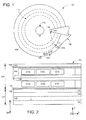
- FIG. 1 generally illustrates a top view block representation of an example data storage device 100 that can utilize a tuned magnetic element in accordance with various embodiments.
- the data storage device 100 is shown in a non-limiting configuration where an actuating assembly 102 is capable of positioning a transducing head 104 over a variety of locations on a magnetic storage media 106 where stored data bits 108 are located on predetermined data tracks 110.
- the storage media 106 can be attached to one or more spindle motors 112 that rotate during use to produce an air bearing surface (ABS) on which a slider portion 114 of the actuating assembly 102 flies to position a head gimbal assembly (HGA) 116, which includes the transducing head 104, over a predetermined portion of the media 106.
- ABS air bearing surface
- HGA head gimbal assembly
- the transducing head 104 can be configured with one or more transducing elements, such as a magnetic writer, magnetically responsive reader, and magnetic shields, which operate to program and read data from the selected data tracks 110 of the storage media 106, respectively.
- controlled motion of the actuating assembly 102 correspond with alignment of the transducers with the data tracks 110 defined on the storage media surfaces to write, read, and rewrite data.
- the head 104 may inadvertently receive magnetic flux from data bits on adjacent data tracks 110, which can induce magnetic noise and interference that degrades performance of the data storage device 100.
- FIG. 2 displays a cross-sectional block representation of an example magnetic element 120 constructed with magnetic shielding to mitigate the effects of reduced form factor data tracks and more densely packed data bits.
- the magnetic element 120 can comprise have one or more data access elements, such as the magnetic reader 122 and writer 124, which can operate individually or concurrently to write data to or retrieve data from an adjacent storage media, such as media 106 of FIG. 1 .
- Each magnetic element 122 and 124 is constructed of a variety of shields and a transducing element that act to read data from and write data to a corresponding data medium along a data track 126.
- the magnetic reading element 122 has a magnetoresistive layer 130 disposed between leading and trailing shields 132 and 134.
- the writing element 124 has a write pole 136 and at least one return pole 138 that creates a writing circuit to impart a predetermined magnetic orientation to the adjacent storage media.
- two return poles 138 are each contactingly adjacent a non-magnetic gap layer 140 and trailing shield 142, respectively, that prevent flux from the poles 136 and 138 from extending beyond the bounds of the writing element 124.
- Each return pole 138 further contacts insulating material 144 that maintains magnetic separation of the writing poles 136 and 138.
- the shields of the magnetic element 120 can be characterized by their position with respect to the timing of encountering external bits, such as bits 108 of FIG. 1 .
- the shields that encounter the external bits before the transducing elements 122 and 124 are “leading” shields while shields that see the bits after the transducing elements are “trailing” shields.
- Such characterization extends to the difference between "uptrack” or “downtrack” of the transducing elements in that, depending on the direction of travel for the magnetic element 120 and external bits, the shields can be either leading or trailing and either uptrack or downtrack.
- the magnetic element 120 has a plurality of shielding layers positioned along the Y axis that dispel magnetic flux from reaching uptrack and downtrack magnetic bits, increased data bit densities have led to the tighter data tracks 126 that correspond with additional shielding along the Z axis.
- the addition of side shields in the Z axis in relation to the write pole 136 can cater the magnetic extent of the write pole 136 to conform to a reduced data track 126 width, but such addition can decrease magnetic field amplitude and gradient as magnetization saturates the side shields instead of flowing through the write pole.
- the reduction in magnetic field can operationally reduce the magnetic sensitivity and data programming efficiency of the write pole 136, which can result in degraded linear data bit density capacity and increased the chances of side track erasure as the write pole inadvertently programs data bits of adjacent data tracks 126.
- FIG. 3 provides an ABS view block representation of a portion of an example magnetic element 150 employing tuned side shields 152 on opposite sides of a write pole 154 in accordance with various embodiments.
- Each side shield 152 is configured with first 156 and second 158 shield sidewalls that taper to a shield tip 160 while the write pole 154 has pole sidewalls 162 that taper to a pole tip 164 positioned uptrack from a pole body 166.
- FIG. 3 is generally illustrated as aligned with a predetermined track where the bottom portion of the magnetic element 150 is uptrack and will encounter a data bit before a downtrack portion at the top plane of the element 150.
- Configuring the side shields 152 with a uniform write gap 168 from the pole body 166 to the pole tip 164 by configuring the shield sidewall 158 angle ( ⁇ 1 ) to match the pole sidewall 162 angle ( ⁇ 2 ) can provide controlled magnetic extent for the write pole 154, but may provide a conduit for magnetic flux to saturate the side shields 152 instead of being transmitted through the write pole 154.
- one or more side shield 152 can be constructed, as shown, so that the shield tip 160 is the closest point between the write pole 154 and the side shield 152.
- the ability to tune the vertical position of the shield tip 160 along the Y axis and the taper angles ( ⁇ 1 & ⁇ 3 ) of the respective shield sidewalls 156 and 158 can control the magnetic extent of the write pole 154 without providing easy magnetic conduits between the write pole 154 and the side shields 152.
- each side shield 152 may be configured so that the shield tip 160 is positioned between the pole tip 164, which can be characterized as the leading edge, and the pole body 166, which can be characterized as the trailing edge, and the shield sidewalls 156 and 158 respectively extend in different directions and angles ( ⁇ 1 & ⁇ 3 ) from the shield tip 160 so that the distance 170 from the pole sidewall 162 to the shield tip 160 is smaller than either distance 172 and 174 from the pole sidewall 162 to the first 156 or second 158 shield sidewall.
- Various embodiments tune the distance 174 to be twice the distance 170 and greater than distance 172 to configure the magnetic extent of the write pole 154 to reduce both side track erasure and adjacent track interference.
- fringe magnetic fields proximal the pole tip 164 can contribute to inadvertent programming of adjacent data tracks in a side track erasure condition. Such condition may be mitigated at least by adjusting the length of the shield sidewalls 156 to extend uptrack from the pole tip 164 a predetermined distance 176, which may be greater than a predetermined width 178 of the pole body 166 at plane 180.
- the magnetic extent of the write pole 154 can be manipulated into a number of different shapes that can increase data writing performance, especially in reduced form factor, high data bit density storage devices.
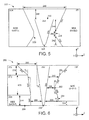
- FIG. 4 illustrates an ABS view block representation of a portion of an example magnetic element 190 tuned with a variety of structural features in accordance with some embodiments.
- the magnetic element 190 has a write pole 192 disposed between side shields 194 and a trailing shield 196 each configured with magnetic extent altering features such as letterbox 198, shield sidewalls 200 and 202, and pole sidewalls 204.
- the write pole 192 is configured with a linear trailing edge 204 and curved leading edge pole tip 206 between which a shield tip 208 is positioned and the shield sidewalls 200 and 202 extend therefrom with lengths that take each sidewall 200 and 202 beyond the bounds of the leading 206 and trailing 204 edges.
- the various sidewalls 200, 202, and 204 can be tuned to an unlimited variety of angles ( ⁇ 1 , ⁇ 2 , & ⁇ 3 ) that allow different shield-to-pole distances at the leading edge 206, trailing edge 204, and shield tip 208.
- the inclusion of a letterbox 198 downtrack from the write pole 192 can provide adequate magnetic shielding while minimizing magnetic flux loss from the pole 192, which increases write field gradient, amplitude, and gain.
- the letterbox 198 is displayed as being formed partially out of the side 194 and trailing 196 shields, but such configuration can be altered, at will, to wholly incorporate the letterbox as part of either the side 194 or trailing 196 shields.
- the position and shape of the letterbox 198 may be tuned in various embodiments to provide a balance between magnetic shielding and write field gain and gradient of the write pole 192. That is, the width 210 and distance 212 from the write pole 198 may be tuned, along with the overall shape such as continuously curvilinear and rectangular, to provide predetermined shielding and magnetic performance characteristics for the write pole 192.
- the addition of a tuned letterbox 198 can reduce magnetic overshoot as stray fields are reduced at least by shape anisotropy provided by the tuned shield sidewalls 200 and 202 having the longest sidewall closest to the write pole 192.
- the letterbox 198 may be complemented by the tuned position of the shield tip 208 provided by leading 214 and trailing 216 distance of the shield tip 208 from the respective leading 206 and trailing 204 edges of the write pole 192 to reduce side track erasure and increase magnetic transition curvature.
- FIG. 5 generally displays an ABS view block representation of a portion of an example magnetic element 220 tuned in accordance with various embodiments.
- the magnetic element 220 has a write pole 222 disposed between side shields 224 that are each tuned to provide more than two shield sidewalls.
- the write pole 222 has a substantially trapezoidal shape with opposite facing pole sidewalls 226 connecting leading 228 and trialing 230 edges.
- Each side shield 224 is configured with first 232 and second 234 shield sidewalls tapering at predetermined angles from a shield tip 236 consisting of a tip sidewall 238.
- the shield tip 236 is not the meeting point of two surfaces but instead a surface having a predetermined length 240 connecting the other shield sidewalls 232 and 234.
- a linear surface for the tip sidewall 238, or alternatively a continuously curvilinear surface in some embodiments provides another tunable structural surface that allows the write gap between the write pole 222 and side shields 224 to vary at predetermined distances 242 and 244 in relation to the pole sidewall 226.
- the shape and position of the tip sidewall 238 can allow the first 232 and second 234 shield sidewalls to taper and extend at angles that would bring the shield sidewalls too close to the write pole 222 if the shield sidewalls 232 and 234 met at a point.
- the length of the tip sidewall 238 may allow the second shield sidewall to extend from the shield tip 236 at a lesser angle to provide a predetermined distance to the trailing edge 230 of the write pole 222 than if the length 240 of the tip sidewall 238 were not present.
- Such lesser shield sidewall angles may be utilized, in some embodiments, to form a predetermined side shield width 246 a predetermined downtrack distance 248 from the write pole 222, which can create letterbox-type write field gain and gradient optimization without the additional manufacturing of a letterbox into the side 224 and/or trailing shields.
- FIG. 6 generally illustrates how an example magnetic element 260 can be tuned to control the magnetic extent of a write pole 262 with differing side shield 264 and 266 configurations constructed in accordance with some embodiments.
- the ABS view of the magnetic element 260 displays a first side shield 264 constructed as a lamination of multiple different materials having different magnetic shielding characteristics and structural orientations.
- the first side shield 264 has first 268, second 270, and third 272 shield layers each having different thicknesses 274, 276, and 278 along the Y axis and different shield sidewalls 280, 282, and 284 oriented with different angles ( ⁇ 1 & ⁇ 2 ) with respect to the pole sidewall 286 ( ⁇ 3 ).
- Some embodiments configure the shield sidewalls 280, 282, and 284 to provide a leading distance 288 between the side shield 264 and the leading edge of the write pole 262 that is half a trailing distance 290 between the side shield 264 and the trailing edge of the write pole 262.
- Configuring the leading distance 288 as half the trailing distance 290 can provide write field optimized for minimum adjacent track interference.
- the increasing write gap between the first side shield 264 and write pole 262 can be complemented by the use of materials exhibiting different magnet moments.
- the first layer 268 can be constructed with a first predetermined moment, such as 2.4 Tesla, while the second layer 270 has a different second predetermined moment, such as 1.4 Tesla, and the third layer 272 is configured with a different third predetermined moment, such as 1.0 Tesla.
- the varying magnetic moments of the different layers 268, 270, and 272 can minimize write field loss as stray magnetic fields are controlled, particularly proximal to the leading pole tip 292.
- the ability to tune the size, position relative to the write pole 262, and material of the various side shield 264 lamination provides additional tuning aspects that can allow precise articulation of the magnetic extent and magnetic characteristics of the write pole 262.
- the second side shield 266 displays how a single layer and material can be constructed with a plurality of shield sidewalls 294, 296, 298, and 300 constructed with different angular orientations ( ⁇ 4 , ⁇ 5 , ⁇ 6 , & ⁇ 7 ) to produce a shield tip 302 that is the closest point between the write pole 262 and the second side shield 266.
- the position of the shield tip 302 may be positioned proximal to any predetermined portion of the pole sidewall 286, but such predetermined portion may be more towards the trailing portion of the write pole 262 when the side shield extends a plane downtrack from the leading pole tip 292. That is, the position of the shield tip 302 may be chosen in response to the downtrack distance 304 the side shield 266 extends. Such downtrack distance 304 may further alter the leading 306, tip 308, and trailing 310 distances to balance magnetic shielding with write field gain and gradient to provide predetermined adjacent track interference and side track erasure mitigation.
- FIG. 7 provides an example magnetic element fabrication routine 330 conducted in accordance with various embodiments to tune the magnetic shielding and magnetic write field performance of a magnetic element. Initially, routine 330 constructs a write pole with a predetermined shape, sidewalls, and pole tip in step 332.
- Step 334 determines whether or not one, or both, side shields are to be constructed as a multi-layer lamination. If a plurality of different side shield layers are to be utilized from decision 334, step 336 successively forms each side shield layer with predetermined materials, thicknesses, and shield sidewall angular orientations. In contrast, step 338 deposits a single side shield layer and forms a shield tip with a predetermined number of shield sidewalls extending therefrom. Various embodiments configure the shield sidewalls to extend beyond the leading and trailing edges of the write pole with other embodiments position the shield tip proximal a predetermined portion of the write pole, such as 10%, 30%, or 50% of the length of the pole sidewall from the leading edge.
- Step 342 forms a letterbox that has a predetermined shape, such as rectangular, trapezoidal, and rectangular shapes, a predetermined size, and a predetermined distance from the write pole.
- a letterbox may incorporate the processing of one, or both, side shields and a trailing shield that is subsequently deposited in step 344. That is, a letterbox may be wholly incorporated into the side or trailing shields or made up of a combination of surfaces provided by both the side and trailing shields.
- step 344 deposits the trailing shield a predetermined distance from the write pole without forming an internal letterbox opening.
- a magnetic element can be optimized for performance by balancing magnetic shielding with write field performance through tuned configurations of the various side shield sidewalls, distances, and shield tip positions.
- the tapered shield sidewalls and position of the shield tip can be configured in a variety of positions relative to the write pole to provide more, or less, magnetic shielding combined with decreased, or minimized, risk of inadvertent performance characteristics, such as side track erasure and adjacent track interference.
- routine 330 shown in FIG. 7 are not required or limited as the various decisions and steps can be omitted, changed, and added.
- decision 334 and steps 336 and 338 can be performed multiple times with similar or different results to construct side shields positioned on opposite sides of the write pole.
- side shield structural parameters that can be tuned to provide predetermined magnetic shielding and data bit programming performance illustrates the vast possible side shield configurations capable of controlling the magnetic extent of a write pole.
- Such side shield configurations may be tuned to provide heightened magnetic field performance with optimized write field gain and gradient while other configurations may be tuned to minimize inadvertent performance conditions resulting from errant magnetic fields and magnetic saturation of the side shields.
- the ability to balance these various performance characteristics by tuning the various structural aspects of the side shields with respect to the write pole conveys the versatility of side shield construction, especially in regard to adapting to increased data bit density, reduced form factor data storage devices.
Landscapes
- Engineering & Computer Science (AREA)
- Manufacturing & Machinery (AREA)
- Physics & Mathematics (AREA)
- Electromagnetism (AREA)
- Magnetic Heads (AREA)
Abstract
Description
- Various embodiments are generally directed to a data writer capable of being used in high data bit density data storage environments.
- In accordance with various embodiments, a write pole may have a pole sidewall and a continuous first taper angle connecting leading and trailing edges. The write pole may be positioned adjacent to a side shield that is configured with first and second shield sidewalls tapered to a shield tip that is the closest point between the write pole and side shield.
- According to a first aspect of the present invention, there is provided an apparatus comprising a write pole having a pole sidewall with a continuous first taper angle connecting leading and trailing edges, the write pole adjacent a side shield configured with first and second shield sidewalls tapered to a shield tip, the shield tip being the closest point between the write pole and side shield.
- Preferably, the shield tip is positioned between the leading and trailing edges.
- Preferably, the first and second shield sidewalls extend from the shield tip at opposing angles.
- Preferably, at least one of the first and second shield sidewalls continuously extend beyond the leading and trailing edges of the write pole.
- Preferably, the first and second shield sidewalls extend from the shield tip at different second and third taper angles.
- Preferably, the shield tip is positioned proximal the leading edge.
- Preferably, the shield tip comprises a linear sidewall with a predetermined length connecting the first and second shield sidewalls.
- More preferably, the linear sidewall is oriented orthogonal to the trailing edge of the write pole.
- Alternatively, it is further preferable that the linear sidewall is positioned wholly between the leading and trailing edges.
- Preferably, the shield tip is positioned a first distance from the leading edge and a second distance from the trailing edge, the first distance being less than the trailing edge.
- According to another aspect of the present invention, there is provided a magnetic element comprising a write pole having a pole sidewall with a continuous first taper angle connecting leading and trailing edges, the write pole disposed between and separated from first and second side shields each configured with first and second shield sidewalls tapered to a shield tip, the shield tip being the closest point between the write pole and side shield.
- Preferably, the first and second side shields have a different total number of shield sidewalls.
- Preferably, at least one of the side shields comprises multiple layers with different magnetic moments.
- Preferably, the multiple layers have different thicknesses.
- Preferably, a first layer of the multiple layers has a first magnetic moment is positioned proximal the leading edge, the first magnetic moment being greater than a second magnetic moment of a second layer of the multiple layers.
- Preferably, the first shield sidewall of both first and second side shields extend beyond the trailing edge to form a letterbox.
- Preferably, the second shield sidewall of at least one of the first and second side shields extends to a plane downtrack from the leading edge.
- According to a further aspect of the present invention, there is provided a data writer comprising a write pole having a pole sidewall with a continuous first taper angle connecting leading and trailing edges, the write pole disposed between and separated from first and second side shields each configured with first and second shield sidewalls tapered to a shield tip and providing a letterbox proximal the trailing edge, the shield tip being the closest point between the write pole and side shield.
- Preferably, the letterbox has a predetermined width greater than a pole width of the write pole.
- Preferably, the letterbox is formed with the union of at least one side shield and a trailing shield.
- Embodiments of the present invention will now be described by way of further example only and with reference to the accompanying drawings, in which:
-
FIG. 1 is a top view block representation of an example data storage device constructed and operated in accordance with various embodiments. -
FIG. 2 illustrates a cross-sectional block representation of an example magnetic element capable of being used in the data storage device ofFIG. 1 . -
FIG. 3 shows an ABS view block representation of a portion of an example magnetic element constructed in accordance with some embodiments. -
FIG. 4 displays an ABS view block representation of a portion of an example magnetic element constructed in accordance with various embodiments. -
FIG. 5 illustrates an ABS view block representation of a portion of an example magnetic element constructed in accordance with various embodiments. -
FIG. 6 is an ABS view block representation of a portion of an example magnetic element constructed in accordance with some embodiments. -
FIG. 7 provides a flowchart for an example magnetic element fabrication routine conducted in accordance with various embodiments. - As data storage devices advance towards greater data storage capacity and faster data access rates, magnetic shielding of errant magnetic flux has become an acute source of manufacturing and operational performance difficulties as the physical size and tolerances of various device components is reduced. While the minimization of data tracks on which data bits populate can pose a particular operational difficulty in the form of adjacent track interference (ATI), positioning lateral magnetic shields adjacent a magnetic access feature, such as a write pole and magnetoresistive lamination, may mitigate ATI by reducing the magnetic extent of the access feature. However, the addition of lateral magnetic shields can suffer from magnetic field and magnetic gradient loss as the magnetic shields saturate with magnetization intended for the magnetic access feature. Hence, there is a continued industry demand for magnetic shield configurations capable of being implemented in reduced form factor data storage devices without decreasing magnetic field and gradient.
- Accordingly, various embodiments can generally be directed to configuring a magnetic element with a write pole having a pole sidewall and a continuous first taper angle connecting leading and trailing edges, where the write pole is positioned adjacent a side shield that is configured with first and second shield sidewalls tapered to a shield tip that is the closest point between the write pole and side shield. The position of the shield tip and the angular orientation of the shield sidewalls from the shield tip in relation to the write pole can be selectively tuned to provide a predetermined magnetic extent. Such tuned magnetic shield configurations can additionally mitigate magnetic flux saturating the shields instead of contributing to data bit access.
- While at least one tuned magnetic shield may be practiced in an unlimited variety of environments,
FIG. 1 generally illustrates a top view block representation of an exampledata storage device 100 that can utilize a tuned magnetic element in accordance with various embodiments. Thedata storage device 100 is shown in a non-limiting configuration where anactuating assembly 102 is capable of positioning a transducinghead 104 over a variety of locations on amagnetic storage media 106 where storeddata bits 108 are located onpredetermined data tracks 110. Thestorage media 106 can be attached to one ormore spindle motors 112 that rotate during use to produce an air bearing surface (ABS) on which aslider portion 114 of theactuating assembly 102 flies to position a head gimbal assembly (HGA) 116, which includes the transducinghead 104, over a predetermined portion of themedia 106. - The transducing
head 104 can be configured with one or more transducing elements, such as a magnetic writer, magnetically responsive reader, and magnetic shields, which operate to program and read data from theselected data tracks 110 of thestorage media 106, respectively. In this way, controlled motion of the actuatingassembly 102 correspond with alignment of the transducers with thedata tracks 110 defined on the storage media surfaces to write, read, and rewrite data. Asdata bits 108 become more densely positioned indata tracks 110 with smaller radial widths, thehead 104 may inadvertently receive magnetic flux from data bits onadjacent data tracks 110, which can induce magnetic noise and interference that degrades performance of thedata storage device 100. -
FIG. 2 displays a cross-sectional block representation of an examplemagnetic element 120 constructed with magnetic shielding to mitigate the effects of reduced form factor data tracks and more densely packed data bits. As shown, themagnetic element 120 can comprise have one or more data access elements, such as themagnetic reader 122 andwriter 124, which can operate individually or concurrently to write data to or retrieve data from an adjacent storage media, such asmedia 106 ofFIG. 1 . Eachmagnetic element data track 126. - The
magnetic reading element 122 has amagnetoresistive layer 130 disposed between leading and trailingshields writing element 124 has awrite pole 136 and at least onereturn pole 138 that creates a writing circuit to impart a predetermined magnetic orientation to the adjacent storage media. In the non-limiting configuration of thewrite element 124 shown inFIG. 2 , tworeturn poles 138 are each contactingly adjacent anon-magnetic gap layer 140 andtrailing shield 142, respectively, that prevent flux from thepoles writing element 124. Eachreturn pole 138 furthercontacts insulating material 144 that maintains magnetic separation of thewriting poles - The shields of the
magnetic element 120 can be characterized by their position with respect to the timing of encountering external bits, such asbits 108 ofFIG. 1 . In other words, the shields that encounter the external bits before the transducingelements magnetic element 120 and external bits, the shields can be either leading or trailing and either uptrack or downtrack. - While the
magnetic element 120 has a plurality of shielding layers positioned along the Y axis that dispel magnetic flux from reaching uptrack and downtrack magnetic bits, increased data bit densities have led to thetighter data tracks 126 that correspond with additional shielding along the Z axis. The addition of side shields in the Z axis in relation to thewrite pole 136 can cater the magnetic extent of thewrite pole 136 to conform to a reduceddata track 126 width, but such addition can decrease magnetic field amplitude and gradient as magnetization saturates the side shields instead of flowing through the write pole. The reduction in magnetic field can operationally reduce the magnetic sensitivity and data programming efficiency of thewrite pole 136, which can result in degraded linear data bit density capacity and increased the chances of side track erasure as the write pole inadvertently programs data bits ofadjacent data tracks 126. -
FIG. 3 provides an ABS view block representation of a portion of an examplemagnetic element 150 employing tunedside shields 152 on opposite sides of awrite pole 154 in accordance with various embodiments. Eachside shield 152 is configured with first 156 and second 158 shield sidewalls that taper to ashield tip 160 while thewrite pole 154 haspole sidewalls 162 that taper to apole tip 164 positioned uptrack from apole body 166. It is to be understood thatFIG. 3 is generally illustrated as aligned with a predetermined track where the bottom portion of themagnetic element 150 is uptrack and will encounter a data bit before a downtrack portion at the top plane of theelement 150. - Configuring the
side shields 152 with auniform write gap 168 from thepole body 166 to thepole tip 164 by configuring theshield sidewall 158 angle (Θ1) to match thepole sidewall 162 angle (Θ2) can provide controlled magnetic extent for thewrite pole 154, but may provide a conduit for magnetic flux to saturate theside shields 152 instead of being transmitted through thewrite pole 154. With such magnetic concerns in mind, one ormore side shield 152 can be constructed, as shown, so that theshield tip 160 is the closest point between thewrite pole 154 and theside shield 152. The ability to tune the vertical position of theshield tip 160 along the Y axis and the taper angles (Θ1 & Θ3) of the respective shield sidewalls 156 and 158 can control the magnetic extent of thewrite pole 154 without providing easy magnetic conduits between thewrite pole 154 and the side shields 152. - As a non-limiting example, each
side shield 152 may be configured so that theshield tip 160 is positioned between thepole tip 164, which can be characterized as the leading edge, and thepole body 166, which can be characterized as the trailing edge, and the shield sidewalls 156 and 158 respectively extend in different directions and angles (Θ1 & Θ3) from theshield tip 160 so that thedistance 170 from thepole sidewall 162 to theshield tip 160 is smaller than eitherdistance pole sidewall 162 to the first 156 or second 158 shield sidewall. Various embodiments tune thedistance 174 to be twice thedistance 170 and greater thandistance 172 to configure the magnetic extent of thewrite pole 154 to reduce both side track erasure and adjacent track interference. - The presence of fringe magnetic fields proximal the
pole tip 164 can contribute to inadvertent programming of adjacent data tracks in a side track erasure condition. Such condition may be mitigated at least by adjusting the length of the shield sidewalls 156 to extend uptrack from the pole tip 164 apredetermined distance 176, which may be greater than apredetermined width 178 of thepole body 166 atplane 180. With the wide variety of tunable magnetic element characteristics like the taper angles (Θ1, Θ2, & Θ3) of theshield shield tip 160, the magnetic extent of thewrite pole 154 can be manipulated into a number of different shapes that can increase data writing performance, especially in reduced form factor, high data bit density storage devices. -
FIG. 4 illustrates an ABS view block representation of a portion of an examplemagnetic element 190 tuned with a variety of structural features in accordance with some embodiments. Themagnetic element 190 has awrite pole 192 disposed between side shields 194 and a trailingshield 196 each configured with magnetic extent altering features such asletterbox 198, shield sidewalls 200 and 202, andpole sidewalls 204. Thewrite pole 192 is configured with alinear trailing edge 204 and curved leadingedge pole tip 206 between which ashield tip 208 is positioned and the shield sidewalls 200 and 202 extend therefrom with lengths that take eachsidewall - As with the shield and pole sidewalls of
FIG. 3 , thevarious sidewalls leading edge 206, trailingedge 204, andshield tip 208. Regardless of the tuned angles of the various sidewalls and size of the gap between theside shield 194 and writepole 192, the inclusion of a letterbox 198 downtrack from thewrite pole 192 can provide adequate magnetic shielding while minimizing magnetic flux loss from thepole 192, which increases write field gradient, amplitude, and gain. The letterbox 198 is displayed as being formed partially out of theside 194 and trailing 196 shields, but such configuration can be altered, at will, to wholly incorporate the letterbox as part of either theside 194 or trailing 196 shields. - The position and shape of the letterbox 198 may be tuned in various embodiments to provide a balance between magnetic shielding and write field gain and gradient of the
write pole 192. That is, thewidth 210 anddistance 212 from thewrite pole 198 may be tuned, along with the overall shape such as continuously curvilinear and rectangular, to provide predetermined shielding and magnetic performance characteristics for thewrite pole 192. The addition of atuned letterbox 198 can reduce magnetic overshoot as stray fields are reduced at least by shape anisotropy provided by the tuned shield sidewalls 200 and 202 having the longest sidewall closest to thewrite pole 192. The letterbox 198 may be complemented by the tuned position of theshield tip 208 provided by leading 214 and trailing 216 distance of theshield tip 208 from the respective leading 206 and trailing 204 edges of thewrite pole 192 to reduce side track erasure and increase magnetic transition curvature. - While the configurations of the side shields 194,
write pole 192, and letterbox 198 can position shielding material in predetermined proximity to selected portions of thewrite pole 192 and allow magnetically insulating material to be disposed between theshields write pole 192, the variousmagnetic element 190 components may further be tuned for shape, material, size, and position to manipulate the magnetic extent of thewrite pole 192 while providing optimized magnetic write fields.FIG. 5 generally displays an ABS view block representation of a portion of an examplemagnetic element 220 tuned in accordance with various embodiments. Themagnetic element 220 has awrite pole 222 disposed between side shields 224 that are each tuned to provide more than two shield sidewalls. - As shown, the
write pole 222 has a substantially trapezoidal shape with opposite facingpole sidewalls 226 connecting leading 228 and trialing 230 edges. Eachside shield 224 is configured with first 232 and second 234 shield sidewalls tapering at predetermined angles from ashield tip 236 consisting of atip sidewall 238. In comparison to theshield tip 208 ofFIG. 4 , theshield tip 236 is not the meeting point of two surfaces but instead a surface having apredetermined length 240 connecting theother shield sidewalls tip sidewall 238, or alternatively a continuously curvilinear surface in some embodiments, provides another tunable structural surface that allows the write gap between thewrite pole 222 andside shields 224 to vary atpredetermined distances pole sidewall 226. - The shape and position of the
tip sidewall 238 can allow the first 232 and second 234 shield sidewalls to taper and extend at angles that would bring the shield sidewalls too close to thewrite pole 222 if the shield sidewalls 232 and 234 met at a point. For example, the length of thetip sidewall 238 may allow the second shield sidewall to extend from theshield tip 236 at a lesser angle to provide a predetermined distance to the trailingedge 230 of thewrite pole 222 than if thelength 240 of thetip sidewall 238 were not present. Such lesser shield sidewall angles may be utilized, in some embodiments, to form a predetermined side shield width 246 apredetermined downtrack distance 248 from thewrite pole 222, which can create letterbox-type write field gain and gradient optimization without the additional manufacturing of a letterbox into theside 224 and/or trailing shields. - The wide variety of shielding configurations possible by tuning the various shield and pole sidewalls are not limited to mirroring structures on opposite sides of the
write pole 222.FIG. 6 generally illustrates how an examplemagnetic element 260 can be tuned to control the magnetic extent of awrite pole 262 with differingside shield magnetic element 260 displays afirst side shield 264 constructed as a lamination of multiple different materials having different magnetic shielding characteristics and structural orientations. - In the example shown in
FIG. 6 , thefirst side shield 264 has first 268, second 270, and third 272 shield layers each havingdifferent thicknesses different shield sidewalls leading distance 288 between theside shield 264 and the leading edge of thewrite pole 262 that is half atrailing distance 290 between theside shield 264 and the trailing edge of thewrite pole 262. Configuring theleading distance 288 as half the trailingdistance 290 can provide write field optimized for minimum adjacent track interference. - The increasing write gap between the
first side shield 264 and writepole 262 can be complemented by the use of materials exhibiting different magnet moments. For example, thefirst layer 268 can be constructed with a first predetermined moment, such as 2.4 Tesla, while thesecond layer 270 has a different second predetermined moment, such as 1.4 Tesla, and thethird layer 272 is configured with a different third predetermined moment, such as 1.0 Tesla. The varying magnetic moments of thedifferent layers leading pole tip 292. The ability to tune the size, position relative to thewrite pole 262, and material of thevarious side shield 264 lamination provides additional tuning aspects that can allow precise articulation of the magnetic extent and magnetic characteristics of thewrite pole 262. - While the use of multiple
different shield layers second side shield 266 displays how a single layer and material can be constructed with a plurality ofshield sidewalls shield tip 302 that is the closest point between thewrite pole 262 and thesecond side shield 266. - The position of the
shield tip 302 may be positioned proximal to any predetermined portion of thepole sidewall 286, but such predetermined portion may be more towards the trailing portion of thewrite pole 262 when the side shield extends a plane downtrack from the leadingpole tip 292. That is, the position of theshield tip 302 may be chosen in response to the downtrack distance 304 theside shield 266 extends. Such downtrack distance 304 may further alter the leading 306,tip 308, and trailing 310 distances to balance magnetic shielding with write field gain and gradient to provide predetermined adjacent track interference and side track erasure mitigation. - With the variety of non-limiting side shield configurations possible to optimize write field and data bit programming performance, the construction of a magnetic element can undergo a series of general and specific decisions to tune the magnetic operation.
FIG. 7 provides an example magneticelement fabrication routine 330 conducted in accordance with various embodiments to tune the magnetic shielding and magnetic write field performance of a magnetic element. Initially, routine 330 constructs a write pole with a predetermined shape, sidewalls, and pole tip instep 332. -
Decision 334 determines whether or not one, or both, side shields are to be constructed as a multi-layer lamination. If a plurality of different side shield layers are to be utilized fromdecision 334, step 336 successively forms each side shield layer with predetermined materials, thicknesses, and shield sidewall angular orientations. In contrast, step 338 deposits a single side shield layer and forms a shield tip with a predetermined number of shield sidewalls extending therefrom. Various embodiments configure the shield sidewalls to extend beyond the leading and trailing edges of the write pole with other embodiments position the shield tip proximal a predetermined portion of the write pole, such as 10%, 30%, or 50% of the length of the pole sidewall from the leading edge. - It should be noted that the formation of side shields on opposite sides of the write pole can be accomplished through performing either
steps decision 340 where the inclusion of letterbox, such asletterbox 198 ofFIG. 4 , is contemplated. Step 342 forms a letterbox that has a predetermined shape, such as rectangular, trapezoidal, and rectangular shapes, a predetermined size, and a predetermined distance from the write pole. Such letterbox construction may incorporate the processing of one, or both, side shields and a trailing shield that is subsequently deposited instep 344. That is, a letterbox may be wholly incorporated into the side or trailing shields or made up of a combination of surfaces provided by both the side and trailing shields. - In the event a letterbox is not to be incorporated into the magnetic element in
decision 340, step 344 deposits the trailing shield a predetermined distance from the write pole without forming an internal letterbox opening. Through the various decisions and steps ofroutine 330, a magnetic element can be optimized for performance by balancing magnetic shielding with write field performance through tuned configurations of the various side shield sidewalls, distances, and shield tip positions. For example, the tapered shield sidewalls and position of the shield tip can be configured in a variety of positions relative to the write pole to provide more, or less, magnetic shielding combined with decreased, or minimized, risk of inadvertent performance characteristics, such as side track erasure and adjacent track interference. - It should be noted, however, that the various steps and decisions of routine 330 shown in
FIG. 7 are not required or limited as the various decisions and steps can be omitted, changed, and added. As an example,decision 334 andsteps - The plethora of side shield structural parameters that can be tuned to provide predetermined magnetic shielding and data bit programming performance illustrates the vast possible side shield configurations capable of controlling the magnetic extent of a write pole. Such side shield configurations may be tuned to provide heightened magnetic field performance with optimized write field gain and gradient while other configurations may be tuned to minimize inadvertent performance conditions resulting from errant magnetic fields and magnetic saturation of the side shields. The ability to balance these various performance characteristics by tuning the various structural aspects of the side shields with respect to the write pole conveys the versatility of side shield construction, especially in regard to adapting to increased data bit density, reduced form factor data storage devices.
- In addition, while the embodiments have been directed to magnetic programming, it will be appreciated that the claimed invention can readily be utilized in any number of other applications, including data storage device applications. It is to be understood that even though numerous characteristics and configurations of various embodiments of the present disclosure have been set forth in the foregoing description, together with details of the structure and function of various embodiments, this detailed description is illustrative only, and changes may be made in detail, especially in matters of structure and arrangements of parts within the principles of the present disclosure to the full extent indicated by the broad general meaning of the terms in which the appended claims are expressed. For example, the particular elements may vary depending on the particular application without departing from the scope of the present technology.
Claims (19)
- An apparatus (150) comprising a write pole (154) having a pole sidewall with a continuous first taper angle Θ2 connecting leading and trailing edges, the write pole adjacent a side shield (152) configured with first and second shield sidewalls (156, 158) tapered to a shield tip (160), the shield tip being the closest point between the write pole and side shield.
- The apparatus of claim 1, wherein the shield tip is positioned between the leading and trailing edges.
- The apparatus of claim 1 or claim 2, wherein the first and second shield sidewalls extend from the shield tip at opposing angles.
- The apparatus of any one of the preceding claims, wherein at least one of the first and second shield sidewalls continuously extend beyond the leading and trailing edges of the write pole.
- The apparatus of any one of the preceding claims, wherein the first and second shield sidewalls extend from the shield tip (208) at different second and third taper angles Θ1, Θ3.
- The apparatus of any one of the preceding claims, wherein the shield tip is positioned proximal the leading edge.
- The apparatus of any one of the preceding claims, wherein the shield tip (238) comprises a linear sidewall with a predetermined length connecting the first and second shield sidewalls.
- The apparatus of claim 7, wherein the linear sidewall is oriented orthogonal to the trailing edge of the write pole.
- The apparatus of claim 7 or claim 8, wherein the linear sidewall is positioned wholly between the leading and trailing edges.
- The apparatus of any one of the preceding claims, wherein the shield tip is positioned a first distance from the leading edge and a second distance from the trailing edge, the first distance being less than the trailing edge.
- The apparatus of any one of the preceding claims, wherein the write pole is disposed between and separated from first and second said side shields (152) each configured with first and second said shield sidewalls tapered to a said shield tip, the shield tip being the closest point between the write pole and side shield.
- The apparatus of claim 11, wherein the first and second side shields (264, 266) have a different total number of shield sidewalls.
- The apparatus of claim 11 or claim 12, wherein at least one of the side shields (264) comprises multiple layers (268, 270, 272) with different magnetic moments.
- The apparatus of claim 13, wherein the multiple layers have different thicknesses.
- The apparatus of claim 13 or claim 14, wherein a first layer of the multiple layers has a first magnetic moment is positioned proximal the leading edge, the first magnetic moment being greater than a second magnetic moment of a second layer of the multiple layers.
- The apparatus any one of claims 11 to 15, wherein the first shield sidewall of both first and second side shields extend beyond the trailing edge to form a letterbox (198).
- The apparatus of claim 16, wherein the letterbox has a predetermined width greater than a pole width of the write pole.
- The apparatus of claim 16 or claim 17, wherein the letterbox is formed with the union of at least one side shield and a trailing shield (196).
- The apparatus of any one of claims 11 to 18, wherein the second shield sidewall of at least one of the first and second side shields extends to a plane downtrack from the leading edge.
Applications Claiming Priority (1)
| Application Number | Priority Date | Filing Date | Title |
|---|---|---|---|
| US13/689,337 US8830625B2 (en) | 2012-11-29 | 2012-11-29 | Data writer with tapered side shield sidewalls |
Publications (2)
| Publication Number | Publication Date |
|---|---|
| EP2738764A1 true EP2738764A1 (en) | 2014-06-04 |
| EP2738764B1 EP2738764B1 (en) | 2017-05-10 |
Family
ID=49641676
Family Applications (1)
| Application Number | Title | Priority Date | Filing Date |
|---|---|---|---|
| EP13194708.7A Not-in-force EP2738764B1 (en) | 2012-11-29 | 2013-11-27 | Data writer with tapered side shield sidewalls |
Country Status (5)
| Country | Link |
|---|---|
| US (2) | US8830625B2 (en) |
| EP (1) | EP2738764B1 (en) |
| JP (1) | JP6013309B2 (en) |
| KR (1) | KR101524527B1 (en) |
| CN (1) | CN103854665B (en) |
Families Citing this family (13)
| Publication number | Priority date | Publication date | Assignee | Title |
|---|---|---|---|---|
| US9196267B2 (en) * | 2013-06-28 | 2015-11-24 | Seagate Technology Llc | Data writer with flux density insert |
| US8964332B1 (en) * | 2013-09-30 | 2015-02-24 | HGST Netherlands B.V. | Microwave-assisted magnetic recording head with asymmetric side gap for shingled magnetic recording |
| US9047889B1 (en) * | 2013-12-10 | 2015-06-02 | HGST Netherlands B.V. | Perpendicular magnetic recording head having a trailing side taper angle which is less than a leading side taper angle |
| US9269378B2 (en) * | 2013-12-20 | 2016-02-23 | HGST Netherlands B.V. | Stray field shielding for perpendicular magnetic recording write head |
| US8988824B1 (en) * | 2013-12-23 | 2015-03-24 | HGST Netherlands B.V. | Method for manufacturing a magnetic write pole with a consistent bevel angle |
| US9224407B2 (en) * | 2014-01-13 | 2015-12-29 | Seagate Technology Llc | Varying write pole side shield gap |
| US9153255B1 (en) * | 2014-03-05 | 2015-10-06 | Western Digital (Fremont), Llc | Method for fabricating a magnetic writer having an asymmetric gap and shields |
| US9286919B1 (en) * | 2014-12-17 | 2016-03-15 | Western Digital (Fremont), Llc | Magnetic writer having a dual side gap |
| US9349388B1 (en) | 2015-02-27 | 2016-05-24 | Seagate Technology Llc | Data writer front shield with varying throat height |
| US9299367B1 (en) | 2015-07-30 | 2016-03-29 | Headway Technologies, Inc. | Perpendicular magnetic recording (PMR) writer with minimized internal flux shunting |
| US9595273B1 (en) * | 2015-09-30 | 2017-03-14 | Western Digital (Fremont), Llc | Shingle magnetic writer having nonconformal shields |
| US10141014B1 (en) | 2017-07-28 | 2018-11-27 | Seagate Technology Llc | Write head with reduced trailing shield—side shield spacing |
| US10468054B1 (en) | 2018-08-22 | 2019-11-05 | Western Digital Technologies, Inc. | Write head having a monolithic side sheild and leading shield |
Citations (5)
| Publication number | Priority date | Publication date | Assignee | Title |
|---|---|---|---|---|
| US20060098334A1 (en) * | 2004-10-27 | 2006-05-11 | Jayasekara Wipul P | Laminated side shield for perpendicular write head for improved performance |
| US20090168240A1 (en) * | 2007-12-28 | 2009-07-02 | Wen-Chien David Hsiao | Perpendicular write head having a modified wrap-around shield to improve overwrite, adjacent track interference and magnetic core width dependence on skew angle |
| US20110058277A1 (en) * | 2009-09-09 | 2011-03-10 | De La Fuente Anton R | Asymmetric writer for shingled magnetic recording |
| US20120106001A1 (en) * | 2010-10-29 | 2012-05-03 | Seagate Technology Llc | Shield with wine glass shaped cavity |
| US20120250187A1 (en) * | 2011-03-28 | 2012-10-04 | Seagate Technology Llc | Write head with modified side shields |
Family Cites Families (38)
| Publication number | Priority date | Publication date | Assignee | Title |
|---|---|---|---|---|
| US5907220A (en) | 1996-03-13 | 1999-05-25 | Applied Materials, Inc. | Magnetron for low pressure full face erosion |
| US5929526A (en) | 1997-06-05 | 1999-07-27 | Micron Technology, Inc. | Removal of metal cusp for improved contact fill |
| US6846745B1 (en) | 2001-08-03 | 2005-01-25 | Novellus Systems, Inc. | High-density plasma process for filling high aspect ratio structures |
| JP4088453B2 (en) * | 2002-02-14 | 2008-05-21 | 株式会社日立グローバルストレージテクノロジーズ | Magnetic head for perpendicular recording and magnetic disk drive equipped with the same |
| JP2004094997A (en) * | 2002-08-29 | 2004-03-25 | Tdk Corp | Thin film magnetic head and its manufacturing method |
| US7205240B2 (en) | 2003-06-04 | 2007-04-17 | Applied Materials, Inc. | HDP-CVD multistep gapfill process |
| US7397633B2 (en) | 2005-03-01 | 2008-07-08 | Seagate Technology, Llc | Writer structure with assisted bias |
| US7268057B2 (en) | 2005-03-30 | 2007-09-11 | Micron Technology, Inc. | Methods of filling openings with oxide, and methods of forming trenched isolation regions |
| KR100763904B1 (en) * | 2005-08-12 | 2007-10-05 | 삼성전자주식회사 | Vertical magnetic head and its manufacturing method |
| JP4287457B2 (en) * | 2006-05-11 | 2009-07-01 | 株式会社東芝 | Magnetic head for perpendicular recording and magnetic disk drive |
| US7715147B2 (en) | 2006-10-27 | 2010-05-11 | Hitachi Global Storage Technologies Netherlands B.V. | Magnetic write head having a shield that extends below the leading edge of the write pole |
| US8689430B1 (en) * | 2006-11-29 | 2014-04-08 | Western Digital (Fremont), Llc | Method for providing a perpendicular magnetic recording (PMR)head |
| US7872835B2 (en) | 2007-04-13 | 2011-01-18 | Headway Technologies, Inc. | Optimized write pole flare angle for side shield or semi side shield PMR writer application |
| US8339735B2 (en) * | 2007-06-29 | 2012-12-25 | Seagate Technology Llc | Magnetic writer for patterned stack with increased write field |
| US8035930B2 (en) | 2007-10-03 | 2011-10-11 | Headway Technologies, Inc. | Perpendicular magnetic recording write head with a side shield |
| US8000064B2 (en) | 2007-12-13 | 2011-08-16 | Tdk Corporation | Thin-film magnetic head for perpendicular magnetic recording and method of making the same |
| US8310782B2 (en) * | 2008-04-04 | 2012-11-13 | Seagate Technology Llc | Dedicated ID-OD writer with beveled pole tips and method of manufacture |
| JP2010003353A (en) | 2008-06-19 | 2010-01-07 | Toshiba Corp | Magnetic recording head, magnetic head assembly, and magnetic recorder |
| US8031433B2 (en) * | 2008-09-05 | 2011-10-04 | Headway Technologies, Inc. | Method to make an integrated side shield PMR head with non conformal side gap |
| JP2010146600A (en) | 2008-12-16 | 2010-07-01 | Hitachi Global Storage Technologies Netherlands Bv | Perpendicular magnetic recording head, method of manufacturing the same, and magnetic recording/reproducing device |
| JP2010146639A (en) | 2008-12-18 | 2010-07-01 | Hitachi Global Storage Technologies Netherlands Bv | Perpendicular recording magnetic head |
| JP2010176732A (en) * | 2009-01-27 | 2010-08-12 | Toshiba Corp | Magnetic head and disk apparatus having the same |
| US8400731B1 (en) * | 2009-04-19 | 2013-03-19 | Western Digital (Fremont), Llc | Write head with variable side shield gaps |
| US8264792B2 (en) | 2009-05-04 | 2012-09-11 | Headway Technologies, Inc. | PMR writer device with multi-level tapered write pole |
| US8470185B2 (en) * | 2009-05-29 | 2013-06-25 | Sae Magnetics (H.K.) Ltd. | Perpendicular magnetic recording head and method of manufacturing the same |
| US8339741B2 (en) * | 2009-06-22 | 2012-12-25 | Seagate Technology Llc | Write pole trailing edge partial side shield |
| JP4693923B2 (en) * | 2009-09-29 | 2011-06-01 | 株式会社東芝 | Magnetic head and disk device provided with the same |
| US8072706B2 (en) | 2009-10-15 | 2011-12-06 | Tdk Corporation | Magnetic head for perpendicular magnetic recording and method of manufacturing same |
| US8134802B2 (en) | 2009-10-29 | 2012-03-13 | Headway Technologies, Inc. | Writer and reader arrangements for shingled writing |
| US8300359B2 (en) * | 2009-12-30 | 2012-10-30 | Tdk Corporation | Perpendicular magnetic recording head and magnetic recording device |
| US8611046B2 (en) * | 2010-04-19 | 2013-12-17 | Headway Technologies, Inc. | PMR writer with graded side shield |
| US8264798B1 (en) * | 2010-06-23 | 2012-09-11 | Western Digital (Fremont), Llc | Systems and methods for providing magnetic recording heads adapted for writing shingled tracks |
| US8355222B2 (en) * | 2010-06-30 | 2013-01-15 | Sae Magnetics (H.K.) Ltd. | Perpendicular magnetic write head including high magnetic moment seed layer for trailing shield therein and/or method of making the same |
| US8347489B2 (en) | 2010-09-01 | 2013-01-08 | Hitachi Global Storage Technologies Netherlands B.V. | Method for manufacturing a perpendicular magnetic write head having a leading edge tapered write pole, self aligned side shield and independent trailing shield |
| US20120154951A1 (en) | 2010-12-21 | 2012-06-21 | Hitachi Global Storage Technologies Netherlands B.V. | Method for manufacturing a perpendicular magnetic write pole having a write pole and trailing shield with a tapered trailing gap |
| US9082425B2 (en) * | 2011-05-04 | 2015-07-14 | Seagate Technology Llc | Magnetic shield with flux concentration feature |
| US8472139B2 (en) * | 2011-09-06 | 2013-06-25 | HGST Netherlands B.V. | Shingled magnetic recording (SMR) head with bent trailing shield and methods of production thereof |
| US8582238B1 (en) * | 2011-10-21 | 2013-11-12 | Western Digital (Fremont), Llc | Systems and methods for providing perpendicular magnetic writers having gradient magnetic moment side shields |
-
2012
- 2012-11-29 US US13/689,337 patent/US8830625B2/en active Active
-
2013
- 2013-11-27 EP EP13194708.7A patent/EP2738764B1/en not_active Not-in-force
- 2013-11-28 JP JP2013246154A patent/JP6013309B2/en not_active Expired - Fee Related
- 2013-11-28 CN CN201310625340.9A patent/CN103854665B/en not_active Expired - Fee Related
- 2013-11-29 KR KR1020130147612A patent/KR101524527B1/en not_active Expired - Fee Related
-
2014
- 2014-09-08 US US14/479,850 patent/US9218824B2/en active Active
Patent Citations (5)
| Publication number | Priority date | Publication date | Assignee | Title |
|---|---|---|---|---|
| US20060098334A1 (en) * | 2004-10-27 | 2006-05-11 | Jayasekara Wipul P | Laminated side shield for perpendicular write head for improved performance |
| US20090168240A1 (en) * | 2007-12-28 | 2009-07-02 | Wen-Chien David Hsiao | Perpendicular write head having a modified wrap-around shield to improve overwrite, adjacent track interference and magnetic core width dependence on skew angle |
| US20110058277A1 (en) * | 2009-09-09 | 2011-03-10 | De La Fuente Anton R | Asymmetric writer for shingled magnetic recording |
| US20120106001A1 (en) * | 2010-10-29 | 2012-05-03 | Seagate Technology Llc | Shield with wine glass shaped cavity |
| US20120250187A1 (en) * | 2011-03-28 | 2012-10-04 | Seagate Technology Llc | Write head with modified side shields |
Also Published As
| Publication number | Publication date |
|---|---|
| US20140146417A1 (en) | 2014-05-29 |
| JP6013309B2 (en) | 2016-10-25 |
| KR20140070469A (en) | 2014-06-10 |
| KR101524527B1 (en) | 2015-06-02 |
| US8830625B2 (en) | 2014-09-09 |
| CN103854665A (en) | 2014-06-11 |
| CN103854665B (en) | 2018-04-10 |
| US20140376131A1 (en) | 2014-12-25 |
| JP2014112455A (en) | 2014-06-19 |
| US9218824B2 (en) | 2015-12-22 |
| EP2738764B1 (en) | 2017-05-10 |
Similar Documents
| Publication | Publication Date | Title |
|---|---|---|
| EP2738764B1 (en) | Data writer with tapered side shield sidewalls | |
| US8830626B2 (en) | Write pole with shaped box shield | |
| US8189294B2 (en) | Apparatus including modified write pole tip | |
| US20100321825A1 (en) | Magnetic writer with multi-component shielf | |
| US8582234B2 (en) | Shaped magnetic write pole | |
| US8472147B2 (en) | Magnetoresistive shield with lateral sub-magnets | |
| CN101345056B (en) | Magnetic writer for patterned media with increased write field | |
| US20140126078A1 (en) | Magnetic writer having multiple gaps with more uniform magnetic fields across the gaps | |
| US8164852B2 (en) | Magnetic head having shield and recording apparatus employing the same | |
| US8675315B2 (en) | Magnetic sensor with anisotropic liner | |
| US9019659B1 (en) | Write pole with varying bevel angles | |
| KR101609730B1 (en) | Side shield with variable anisotropy | |
| US8804283B2 (en) | Chamfered magnetic write pole | |
| EP2728579A2 (en) | Magnetic element with current constriction feature | |
| US9704510B2 (en) | Data writer with graded side shields | |
| KR20150035892A (en) | Data writer with tapered side shield sidewalls | |
| US20170133043A1 (en) | Single coil turn data writer | |
| US9099108B2 (en) | Magnetically biased write pole | |
| US20140300995A1 (en) | Data Writer with Yoke Shaped Write Pole | |
| US9263066B1 (en) | Data writer with magnetically hard front shield |
Legal Events
| Date | Code | Title | Description |
|---|---|---|---|
| PUAI | Public reference made under article 153(3) epc to a published international application that has entered the european phase |
Free format text: ORIGINAL CODE: 0009012 |
|
| 17P | Request for examination filed |
Effective date: 20131216 |
|
| AK | Designated contracting states |
Kind code of ref document: A1 Designated state(s): AL AT BE BG CH CY CZ DE DK EE ES FI FR GB GR HR HU IE IS IT LI LT LU LV MC MK MT NL NO PL PT RO RS SE SI SK SM TR |
|
| AX | Request for extension of the european patent |
Extension state: BA ME |
|
| RIN1 | Information on inventor provided before grant (corrected) |
Inventor name: XUE, JIANHUA Inventor name: CHEN, YONGHUA Inventor name: LINVILLE, ERIC SHANE Inventor name: YIN, HUAQING Inventor name: MELOCHE, ERIC ROGER |
|
| RBV | Designated contracting states (corrected) |
Designated state(s): AL AT BE BG CH CY CZ DE DK EE ES FI FR GB GR HR HU IE IS IT LI LT LU LV MC MK MT NL NO PL PT RO RS SE SI SK SM TR |
|
| 17Q | First examination report despatched |
Effective date: 20150722 |
|
| REG | Reference to a national code |
Ref country code: DE Ref legal event code: R079 Ref document number: 602013020889 Country of ref document: DE Free format text: PREVIOUS MAIN CLASS: G11B0005127000 Ipc: G11B0005110000 |
|
| GRAP | Despatch of communication of intention to grant a patent |
Free format text: ORIGINAL CODE: EPIDOSNIGR1 |
|
| RIC1 | Information provided on ipc code assigned before grant |
Ipc: G11B 5/11 20060101AFI20161108BHEP Ipc: G11B 5/31 20060101ALI20161108BHEP Ipc: G11B 5/127 20060101ALI20161108BHEP |
|
| INTG | Intention to grant announced |
Effective date: 20161124 |
|
| GRAS | Grant fee paid |
Free format text: ORIGINAL CODE: EPIDOSNIGR3 |
|
| GRAA | (expected) grant |
Free format text: ORIGINAL CODE: 0009210 |
|
| AK | Designated contracting states |
Kind code of ref document: B1 Designated state(s): AL AT BE BG CH CY CZ DE DK EE ES FI FR GB GR HR HU IE IS IT LI LT LU LV MC MK MT NL NO PL PT RO RS SE SI SK SM TR |
|
| REG | Reference to a national code |
Ref country code: GB Ref legal event code: FG4D |
|
| REG | Reference to a national code |
Ref country code: AT Ref legal event code: REF Ref document number: 893101 Country of ref document: AT Kind code of ref document: T Effective date: 20170515 Ref country code: CH Ref legal event code: EP |
|
| REG | Reference to a national code |
Ref country code: IE Ref legal event code: FG4D |
|
| REG | Reference to a national code |
Ref country code: DE Ref legal event code: R096 Ref document number: 602013020889 Country of ref document: DE |
|
| REG | Reference to a national code |
Ref country code: NL Ref legal event code: MP Effective date: 20170510 |
|
| REG | Reference to a national code |
Ref country code: LT Ref legal event code: MG4D |
|
| REG | Reference to a national code |
Ref country code: AT Ref legal event code: MK05 Ref document number: 893101 Country of ref document: AT Kind code of ref document: T Effective date: 20170510 |
|
| PG25 | Lapsed in a contracting state [announced via postgrant information from national office to epo] |
Ref country code: AT Free format text: LAPSE BECAUSE OF FAILURE TO SUBMIT A TRANSLATION OF THE DESCRIPTION OR TO PAY THE FEE WITHIN THE PRESCRIBED TIME-LIMIT Effective date: 20170510 Ref country code: NO Free format text: LAPSE BECAUSE OF FAILURE TO SUBMIT A TRANSLATION OF THE DESCRIPTION OR TO PAY THE FEE WITHIN THE PRESCRIBED TIME-LIMIT Effective date: 20170810 Ref country code: HR Free format text: LAPSE BECAUSE OF FAILURE TO SUBMIT A TRANSLATION OF THE DESCRIPTION OR TO PAY THE FEE WITHIN THE PRESCRIBED TIME-LIMIT Effective date: 20170510 Ref country code: GR Free format text: LAPSE BECAUSE OF FAILURE TO SUBMIT A TRANSLATION OF THE DESCRIPTION OR TO PAY THE FEE WITHIN THE PRESCRIBED TIME-LIMIT Effective date: 20170811 Ref country code: FI Free format text: LAPSE BECAUSE OF FAILURE TO SUBMIT A TRANSLATION OF THE DESCRIPTION OR TO PAY THE FEE WITHIN THE PRESCRIBED TIME-LIMIT Effective date: 20170510 Ref country code: ES Free format text: LAPSE BECAUSE OF FAILURE TO SUBMIT A TRANSLATION OF THE DESCRIPTION OR TO PAY THE FEE WITHIN THE PRESCRIBED TIME-LIMIT Effective date: 20170510 Ref country code: LT Free format text: LAPSE BECAUSE OF FAILURE TO SUBMIT A TRANSLATION OF THE DESCRIPTION OR TO PAY THE FEE WITHIN THE PRESCRIBED TIME-LIMIT Effective date: 20170510 |
|
| PG25 | Lapsed in a contracting state [announced via postgrant information from national office to epo] |
Ref country code: SE Free format text: LAPSE BECAUSE OF FAILURE TO SUBMIT A TRANSLATION OF THE DESCRIPTION OR TO PAY THE FEE WITHIN THE PRESCRIBED TIME-LIMIT Effective date: 20170510 Ref country code: PL Free format text: LAPSE BECAUSE OF FAILURE TO SUBMIT A TRANSLATION OF THE DESCRIPTION OR TO PAY THE FEE WITHIN THE PRESCRIBED TIME-LIMIT Effective date: 20170510 Ref country code: RS Free format text: LAPSE BECAUSE OF FAILURE TO SUBMIT A TRANSLATION OF THE DESCRIPTION OR TO PAY THE FEE WITHIN THE PRESCRIBED TIME-LIMIT Effective date: 20170510 Ref country code: BG Free format text: LAPSE BECAUSE OF FAILURE TO SUBMIT A TRANSLATION OF THE DESCRIPTION OR TO PAY THE FEE WITHIN THE PRESCRIBED TIME-LIMIT Effective date: 20170810 Ref country code: LV Free format text: LAPSE BECAUSE OF FAILURE TO SUBMIT A TRANSLATION OF THE DESCRIPTION OR TO PAY THE FEE WITHIN THE PRESCRIBED TIME-LIMIT Effective date: 20170510 Ref country code: NL Free format text: LAPSE BECAUSE OF FAILURE TO SUBMIT A TRANSLATION OF THE DESCRIPTION OR TO PAY THE FEE WITHIN THE PRESCRIBED TIME-LIMIT Effective date: 20170510 Ref country code: IS Free format text: LAPSE BECAUSE OF FAILURE TO SUBMIT A TRANSLATION OF THE DESCRIPTION OR TO PAY THE FEE WITHIN THE PRESCRIBED TIME-LIMIT Effective date: 20170910 |
|
| PG25 | Lapsed in a contracting state [announced via postgrant information from national office to epo] |
Ref country code: RO Free format text: LAPSE BECAUSE OF FAILURE TO SUBMIT A TRANSLATION OF THE DESCRIPTION OR TO PAY THE FEE WITHIN THE PRESCRIBED TIME-LIMIT Effective date: 20170510 Ref country code: CZ Free format text: LAPSE BECAUSE OF FAILURE TO SUBMIT A TRANSLATION OF THE DESCRIPTION OR TO PAY THE FEE WITHIN THE PRESCRIBED TIME-LIMIT Effective date: 20170510 Ref country code: DK Free format text: LAPSE BECAUSE OF FAILURE TO SUBMIT A TRANSLATION OF THE DESCRIPTION OR TO PAY THE FEE WITHIN THE PRESCRIBED TIME-LIMIT Effective date: 20170510 Ref country code: EE Free format text: LAPSE BECAUSE OF FAILURE TO SUBMIT A TRANSLATION OF THE DESCRIPTION OR TO PAY THE FEE WITHIN THE PRESCRIBED TIME-LIMIT Effective date: 20170510 Ref country code: SK Free format text: LAPSE BECAUSE OF FAILURE TO SUBMIT A TRANSLATION OF THE DESCRIPTION OR TO PAY THE FEE WITHIN THE PRESCRIBED TIME-LIMIT Effective date: 20170510 |
|
| REG | Reference to a national code |
Ref country code: DE Ref legal event code: R097 Ref document number: 602013020889 Country of ref document: DE |
|
| PG25 | Lapsed in a contracting state [announced via postgrant information from national office to epo] |
Ref country code: SM Free format text: LAPSE BECAUSE OF FAILURE TO SUBMIT A TRANSLATION OF THE DESCRIPTION OR TO PAY THE FEE WITHIN THE PRESCRIBED TIME-LIMIT Effective date: 20170510 Ref country code: IT Free format text: LAPSE BECAUSE OF FAILURE TO SUBMIT A TRANSLATION OF THE DESCRIPTION OR TO PAY THE FEE WITHIN THE PRESCRIBED TIME-LIMIT Effective date: 20170510 |
|
| PLBE | No opposition filed within time limit |
Free format text: ORIGINAL CODE: 0009261 |
|
| STAA | Information on the status of an ep patent application or granted ep patent |
Free format text: STATUS: NO OPPOSITION FILED WITHIN TIME LIMIT |
|
| 26N | No opposition filed |
Effective date: 20180213 |
|
| PG25 | Lapsed in a contracting state [announced via postgrant information from national office to epo] |
Ref country code: SI Free format text: LAPSE BECAUSE OF FAILURE TO SUBMIT A TRANSLATION OF THE DESCRIPTION OR TO PAY THE FEE WITHIN THE PRESCRIBED TIME-LIMIT Effective date: 20170510 |
|
| REG | Reference to a national code |
Ref country code: DE Ref legal event code: R119 Ref document number: 602013020889 Country of ref document: DE |
|
| PG25 | Lapsed in a contracting state [announced via postgrant information from national office to epo] |
Ref country code: MC Free format text: LAPSE BECAUSE OF FAILURE TO SUBMIT A TRANSLATION OF THE DESCRIPTION OR TO PAY THE FEE WITHIN THE PRESCRIBED TIME-LIMIT Effective date: 20170510 |
|
| GBPC | Gb: european patent ceased through non-payment of renewal fee |
Effective date: 20171127 |
|
| PG25 | Lapsed in a contracting state [announced via postgrant information from national office to epo] |
Ref country code: CH Free format text: LAPSE BECAUSE OF NON-PAYMENT OF DUE FEES Effective date: 20171130 Ref country code: LI Free format text: LAPSE BECAUSE OF NON-PAYMENT OF DUE FEES Effective date: 20171130 |
|
| PG25 | Lapsed in a contracting state [announced via postgrant information from national office to epo] |
Ref country code: LU Free format text: LAPSE BECAUSE OF NON-PAYMENT OF DUE FEES Effective date: 20171127 |
|
| REG | Reference to a national code |
Ref country code: FR Ref legal event code: ST Effective date: 20180731 Ref country code: BE Ref legal event code: MM Effective date: 20171130 |
|
| REG | Reference to a national code |
Ref country code: IE Ref legal event code: MM4A |
|
| PG25 | Lapsed in a contracting state [announced via postgrant information from national office to epo] |
Ref country code: MT Free format text: LAPSE BECAUSE OF NON-PAYMENT OF DUE FEES Effective date: 20171127 |
|
| PG25 | Lapsed in a contracting state [announced via postgrant information from national office to epo] |
Ref country code: DE Free format text: LAPSE BECAUSE OF NON-PAYMENT OF DUE FEES Effective date: 20180602 Ref country code: FR Free format text: LAPSE BECAUSE OF NON-PAYMENT OF DUE FEES Effective date: 20171130 Ref country code: IE Free format text: LAPSE BECAUSE OF NON-PAYMENT OF DUE FEES Effective date: 20171127 |
|
| PG25 | Lapsed in a contracting state [announced via postgrant information from national office to epo] |
Ref country code: BE Free format text: LAPSE BECAUSE OF NON-PAYMENT OF DUE FEES Effective date: 20171130 Ref country code: GB Free format text: LAPSE BECAUSE OF NON-PAYMENT OF DUE FEES Effective date: 20171127 |
|
| PG25 | Lapsed in a contracting state [announced via postgrant information from national office to epo] |
Ref country code: HU Free format text: LAPSE BECAUSE OF FAILURE TO SUBMIT A TRANSLATION OF THE DESCRIPTION OR TO PAY THE FEE WITHIN THE PRESCRIBED TIME-LIMIT; INVALID AB INITIO Effective date: 20131127 |
|
| PG25 | Lapsed in a contracting state [announced via postgrant information from national office to epo] |
Ref country code: CY Free format text: LAPSE BECAUSE OF NON-PAYMENT OF DUE FEES Effective date: 20170510 |
|
| PG25 | Lapsed in a contracting state [announced via postgrant information from national office to epo] |
Ref country code: MK Free format text: LAPSE BECAUSE OF FAILURE TO SUBMIT A TRANSLATION OF THE DESCRIPTION OR TO PAY THE FEE WITHIN THE PRESCRIBED TIME-LIMIT Effective date: 20170510 |
|
| PG25 | Lapsed in a contracting state [announced via postgrant information from national office to epo] |
Ref country code: TR Free format text: LAPSE BECAUSE OF FAILURE TO SUBMIT A TRANSLATION OF THE DESCRIPTION OR TO PAY THE FEE WITHIN THE PRESCRIBED TIME-LIMIT Effective date: 20170510 |
|
| PG25 | Lapsed in a contracting state [announced via postgrant information from national office to epo] |
Ref country code: PT Free format text: LAPSE BECAUSE OF FAILURE TO SUBMIT A TRANSLATION OF THE DESCRIPTION OR TO PAY THE FEE WITHIN THE PRESCRIBED TIME-LIMIT Effective date: 20170510 |
|
| PG25 | Lapsed in a contracting state [announced via postgrant information from national office to epo] |
Ref country code: AL Free format text: LAPSE BECAUSE OF FAILURE TO SUBMIT A TRANSLATION OF THE DESCRIPTION OR TO PAY THE FEE WITHIN THE PRESCRIBED TIME-LIMIT Effective date: 20170510 |