EP2738758B1 - Gate driving apparatus and display device - Google Patents
Gate driving apparatus and display device Download PDFInfo
- Publication number
- EP2738758B1 EP2738758B1 EP13194861.4A EP13194861A EP2738758B1 EP 2738758 B1 EP2738758 B1 EP 2738758B1 EP 13194861 A EP13194861 A EP 13194861A EP 2738758 B1 EP2738758 B1 EP 2738758B1
- Authority
- EP
- European Patent Office
- Prior art keywords
- shift register
- pulling
- unit
- terminal
- thin film
- Prior art date
- Legal status (The legal status is an assumption and is not a legal conclusion. Google has not performed a legal analysis and makes no representation as to the accuracy of the status listed.)
- Not-in-force
Links
Images


Classifications
-
- G—PHYSICS
- G09—EDUCATION; CRYPTOGRAPHY; DISPLAY; ADVERTISING; SEALS
- G09G—ARRANGEMENTS OR CIRCUITS FOR CONTROL OF INDICATING DEVICES USING STATIC MEANS TO PRESENT VARIABLE INFORMATION
- G09G3/00—Control arrangements or circuits, of interest only in connection with visual indicators other than cathode-ray tubes
- G09G3/20—Control arrangements or circuits, of interest only in connection with visual indicators other than cathode-ray tubes for presentation of an assembly of a number of characters, e.g. a page, by composing the assembly by combination of individual elements arranged in a matrix no fixed position being assigned to or needed to be assigned to the individual characters or partial characters
- G09G3/34—Control arrangements or circuits, of interest only in connection with visual indicators other than cathode-ray tubes for presentation of an assembly of a number of characters, e.g. a page, by composing the assembly by combination of individual elements arranged in a matrix no fixed position being assigned to or needed to be assigned to the individual characters or partial characters by control of light from an independent source
- G09G3/36—Control arrangements or circuits, of interest only in connection with visual indicators other than cathode-ray tubes for presentation of an assembly of a number of characters, e.g. a page, by composing the assembly by combination of individual elements arranged in a matrix no fixed position being assigned to or needed to be assigned to the individual characters or partial characters by control of light from an independent source using liquid crystals
- G09G3/3611—Control of matrices with row and column drivers
- G09G3/3674—Details of drivers for scan electrodes
- G09G3/3677—Details of drivers for scan electrodes suitable for active matrices only
-
- G—PHYSICS
- G09—EDUCATION; CRYPTOGRAPHY; DISPLAY; ADVERTISING; SEALS
- G09G—ARRANGEMENTS OR CIRCUITS FOR CONTROL OF INDICATING DEVICES USING STATIC MEANS TO PRESENT VARIABLE INFORMATION
- G09G3/00—Control arrangements or circuits, of interest only in connection with visual indicators other than cathode-ray tubes
- G09G3/20—Control arrangements or circuits, of interest only in connection with visual indicators other than cathode-ray tubes for presentation of an assembly of a number of characters, e.g. a page, by composing the assembly by combination of individual elements arranged in a matrix no fixed position being assigned to or needed to be assigned to the individual characters or partial characters
- G09G3/34—Control arrangements or circuits, of interest only in connection with visual indicators other than cathode-ray tubes for presentation of an assembly of a number of characters, e.g. a page, by composing the assembly by combination of individual elements arranged in a matrix no fixed position being assigned to or needed to be assigned to the individual characters or partial characters by control of light from an independent source
- G09G3/36—Control arrangements or circuits, of interest only in connection with visual indicators other than cathode-ray tubes for presentation of an assembly of a number of characters, e.g. a page, by composing the assembly by combination of individual elements arranged in a matrix no fixed position being assigned to or needed to be assigned to the individual characters or partial characters by control of light from an independent source using liquid crystals
- G09G3/3611—Control of matrices with row and column drivers
- G09G3/3674—Details of drivers for scan electrodes
-
- G—PHYSICS
- G11—INFORMATION STORAGE
- G11C—STATIC STORES
- G11C19/00—Digital stores in which the information is moved stepwise, e.g. shift registers
- G11C19/28—Digital stores in which the information is moved stepwise, e.g. shift registers using semiconductor elements
-
- G—PHYSICS
- G09—EDUCATION; CRYPTOGRAPHY; DISPLAY; ADVERTISING; SEALS
- G09G—ARRANGEMENTS OR CIRCUITS FOR CONTROL OF INDICATING DEVICES USING STATIC MEANS TO PRESENT VARIABLE INFORMATION
- G09G2300/00—Aspects of the constitution of display devices
- G09G2300/04—Structural and physical details of display devices
- G09G2300/0404—Matrix technologies
- G09G2300/0408—Integration of the drivers onto the display substrate
-
- G—PHYSICS
- G09—EDUCATION; CRYPTOGRAPHY; DISPLAY; ADVERTISING; SEALS
- G09G—ARRANGEMENTS OR CIRCUITS FOR CONTROL OF INDICATING DEVICES USING STATIC MEANS TO PRESENT VARIABLE INFORMATION
- G09G2310/00—Command of the display device
- G09G2310/02—Addressing, scanning or driving the display screen or processing steps related thereto
- G09G2310/0264—Details of driving circuits
- G09G2310/0286—Details of a shift registers arranged for use in a driving circuit
-
- G—PHYSICS
- G09—EDUCATION; CRYPTOGRAPHY; DISPLAY; ADVERTISING; SEALS
- G09G—ARRANGEMENTS OR CIRCUITS FOR CONTROL OF INDICATING DEVICES USING STATIC MEANS TO PRESENT VARIABLE INFORMATION
- G09G2310/00—Command of the display device
- G09G2310/02—Addressing, scanning or driving the display screen or processing steps related thereto
- G09G2310/0264—Details of driving circuits
- G09G2310/0291—Details of output amplifiers or buffers arranged for use in a driving circuit
Definitions
- the present disclosure relates to a field of liquid crystal displaying technique, and particularly, to a gate driving apparatus and a display device.
- a liquid crystal display device has filled in everywhere in people's life, such as a mobile phone, a game machine, a computer display, a television and the like.
- a traditional liquid crystal display device drives a liquid crystal panel to display generally in a manner of bonding by a gate driving IC and a source driving IC, and a driving technique for disposing a gate driver on the liquid crystal display integrally (gate in panel, GIP) arises to meet requirements for an increased resolution and a competitive cost pressure.
- a gate driving circuit is composed of a plurality of thin film transistors TFTs, its manufacture process is the same as the liquid crystal display, which can reduce expenses of using the gate driving IC without increasing process difficulty and the cost.
- Fig.1 is a schematic diagram illustrating a liquid crystal display driven by the existing GIP technique.
- a gate driving apparatus is composed of a plurality of shift register units 1 connected in cascade, each of the shift register units corresponds to a gate driving signal line, wherein a STV (frame start signal) provides a start signal with a cycle being same as a frame frequency to the shift register unit S 1; a first clock signal CLK and a second clock signal CLKB are the same but have opposite polarities, and are used for controlling the shift register to output a high level signal or a low level signal.
- a low level maintaining signal is provided to the shift register by VSS.
- An output signal from the shift register unit S1 is as a start signal for a next shift register unit S2 and provides a reset signal to the shift register unit S1 at the same time when the shift register unit S2 outputs a high level, so that the output from the S 1 is at the low level to produce a progressive driving process of the liquid crystal display device.
- CN 102 708 925 A discloses a TFT shift register which comprises a shift register functional part and an auxiliary part, the shift register functional part is used for realizing a shift register function, the auxiliary part is used for controlling the voltage of a pulling low point in the shift register functional part, assisting charge and discharge of a PU point and an output terminal, and controlling output noise.
- the signal output from the shift register may change abnormally when a short-circuit occurs in the wirings associated with the gate driving signal lines (for example, a gate signal line and a data signal line, the gate signal line and a common electrode line) within the panel of the liquid crystal display device, which may affect visibly the resetting of the previous shift register and the turning-on of the next shift register and in turn cause a disorder in timings and operation states of all of the shift registers, such that a display in a full screen is abnormal or fails.
- This problem may also affect seriously the research and analysis of reasons for the defect of the abnormality in a picture displaying, which will be made by engineers, and it is not benefit for increasing the product yield.
- the gate driving apparatus according to the embodiments of the present disclosure comprises the features of claim 1.
- a display device comprises the above gate driving apparatus.
- the embodiments of the present disclosure may settle an abnormal display in a full screen caused by an abnormality in signals output from a shift register, when a short-circuit occurs in wirings associated with gate lines within a liquid crystal panel, by arranging the outputting unit at the output terminal of the shift register unit, making an output signal from the shift register unit of the gate driving apparatus as a pulling-up control signal of the outputting unit, and providing an output signal to the gate line by the outputting unit, while it is able to enhance an analysis efficiency for defective phenomena such as the normal display, etc, and increase the product yield.
- Embodiments of the present disclosure provide a gate driving apparatus and a display device for settling an abnormal displaying in a full screen caused by an abnormality in signals output from a shift register when short-circuit occurs in wirings associated with gate lines within a liquid crystal panel.
- the gate driving apparatus comprises a plurality of gate driving units 2 connected in cascade, wherein each stage of the gate driving unit 2 comprises a shift register unit 3, for example, S1, S2, etc. in Fig. 2 .
- the shift register unit 3 comprises a pulling-down control node PD-CN.
- Each stage of the gate driving unit 2 further comprises an outputting unit 4, for example, Z1, Z2 and the like in the figure, for outputting a first power voltage Vgh or a second power voltage VSS to a gate line.
- a pulling-up control terminal IN of the outputting unit is connected to an output terminal OUTPUT of the shift register unit, a reset signal terminal RET thereof is connected to a reset signal terminal RET of the shift register unit in the same stage of the gate driving unit, a pulling-down control terminal thereof is connected to a pulling-down control node PD-CN of the shift register unit in the same stage of the gate driving unit, a first power supply input terminal thereof is connected to the first power voltage Vgh, a second power supply input terminal thereof is connected to the second power voltage VSS, and an output terminal OUT of the outputting unit is connected to the gate line 'gate' as an output terminal of the gate driving unit.
- the outputting unit 4 comprises:
- the first outputting module comprises a first thin film transistor with a gate connected to the pulling-up control terminal of the outputting unit, a source connected to the first power supply input terminal, and a drain connected to the output terminal of the outputting unit.
- the second outputting module comprises a second thin film transistor with a gate connected to the reset signal terminal of the outputting unit, a source connected to the output terminal of the outputting unit, and a drain connected to the second power supply input terminal.
- the third outputting module comprises a third thin film transistor with a gate connected to the pulling-down control terminal of the outputting unit, a source connected to the output terminal of the outputting unit, and a drain connected to the second power supply input terminal.
- the shift register unit comprises a plurality of N-type thin film transistors, and the first thin film transistor, the second thin film transistor and the third thin film transistor in the outputting unit are all the N-type thin film transistors.
- the N-type thin film transistor is turned on at a high level and is turned off at a low level.
- an input signal terminal of a first stage of shift register unit is connected to a frame start signal, and a reset signal terminal of the first stage of shift register unit is connected to an output terminal of a second stage of shift register unit;
- an input signal terminal of a last stage of shift register unit is connected to an output terminal of a previous stage of shift register unit, and a reset signal terminal of the last stage of shift register unit is connected to the frame start signal, or is connected to an outputting terminal of any stage of shift register unit except its previous stage of shift register unit or an output terminal of the outputting unit;
- the input signal terminals of the remaining respective stages of shift register units are connected to the output terminals of their corresponding previous stages of shift register units, and the reset signal terminals thereof are connected to the output terminals of the next stages of shift register units.
- the gate driving apparatus comprises a plurality of gate driving units 2 connected in cascade, wherein each stage of the gate driving unit 2 comprises a shift register unit 3, for example, S1, S2, and the like in the figure, which comprises a pulling-down control node PD-CN, and each stage of the gate driving unit further comprises an outputting unit 4, for example, Z1, Z2 and the like in the figure.
- a pulling-up control terminal IN of the outputting unit is connected to an output terminal OUTPUT of the shift register unit, a reset signal terminal RET thereof is connected to a reset signal terminal RET of the shift register unit, a pulling-down control terminal thereof is connected to a pulling-down control node PD-CN of the shift register unit, a first power supply input terminal thereof is connected to the first power voltage Vgh, a second power supply input terminal thereof is connected to the second power voltage VSS, and an output terminal OUT of the outputting unit is connected to the gate line 'gate' as an output terminal of the gate driving unit.
- the first power voltage Vgh is a high level
- the second power voltage VSS is a low level.
- An input signal terminal IN of the first stage of shift register unit S1 is connected to a frame start signal STV
- the reset signal terminal RET of the first stage of shift register unit S1 is connected to an output terminal OUTPUT of the second stage of shift register unit
- an input signal terminal of the last stage of shift register unit is connected to an output terminal of its previous stage of shift register unit
- a reset signal terminal of the last stage of shift register unit is connected to the frame start signal, or is connected to an output terminal of any stage of shift register unit except its previous stage of shift register unit or an output terminal of an outputting unit 4; except for the first stage of shift register unit and the last stage of shift register unit, the input signal terminals of the remaining respective stages of shift register units are connected to the output terminals of previous stages of shift register units, and the reset signal terminals thereof are connected to the output terminals of next stages of shift register units.
- a STV as the frame start signal, provides a driving start control signal to the shift register
- CLK and CLKB are a first clock signal and a second clock signal, respectively, and control the shift register to output a high level signal and a low level signal, respectively
- a VSS provides a low level maintaining signal to the shift register 3 and the outputting unit 4
- a Vgh provides a high level signal to a gate signal line through the outputting unit 4
- a high level signal output from the outputting unit 4 is controlled by an output signal from the shift register 3.
- a pulse cycle of the STV is the same as a frame frequency of a display device
- the CLK and the CLKB have the same signal pulses but opposite polarities
- the Vgh and the VSS are the high level signal and the low level signal, respectively.
- an output signal at the high level from the shift register unit S1 functions as an input signal of the shift register unit S2 in the second gate driving unit; when the second gate driving unit outputs a high level, the output signal at the high level from the shift register unit S2 functions as a reset signal of the shift register unit S1 and the outputting unit Z1 (which makes the output from the shift register unit S1 and the gate signal be at the low levels); and when the S1 and Z1 are reset to the low level, the shift register S1 outputs a PD-CN signal to the outputting unit Z1 so as to maintain the output terminal of the outputting unit Z1 at the low level.
- the gate signal lines corresponding to each of the gate driving units outputs progressively a high level to drive a liquid crystal panel to drive progressively the display.
- the gate driving apparatus is always maintained to output the low level outside periods of time during which it outputs the high level.
- Fig. 3 is a schematic diagram illustrating a circuit structure of a shift register unit connected in cascade in the prior art.
- the shift register unit is used for the prior art shown in Fig. 1 and also may be used for the structure of the gate driving apparatus according to the embodiment of the present disclosure illustrated in Fig. 2 .
- regions marked by reference numerals 11, 12, 13, 14 and 15 correspond to a pulling-up driving module, a pulling-up module, a pulling-down controlling module, a pulling-down module and a resetting module in the shift register, respectively.
- the pulling-up driving module 11 of the shift register unit comprises a TFT M1 with a gate and a source connected to a STV signal, and a drain connected to a PU node;
- the pulling-up module 12 comprises a TFT M3 and a capacitor C1, a source of the M3 is connected to a first clock signal CLK, a gate thereof is connected to the PU node, and a drain thereof is connected to an output terminal OUTPUT; a first end of the capacitor C1 is connected to the PU node, and a second end thereof is connected to the output terminal OUTPUT;
- the pulling-down controlling module 13 comprises a TFT M6 with a gate connected to the PU node, a drain connected to a VSS, and a source used as a PD-CN node;
- the pulling-down module 14 comprises TFTs M2, M4, M5 and M8, wherein a source of the M2 is connected to the PU node, a gate thereof is connected to the a
- the pulling-up driving module 11 receives the high level signal outputting from the previous stage as a start signal, so that a level at the PU node connected with the pulling-up module 12 rises and a level at the PD-CN node is pulled down; when the first clock signal CLK is at the high level, the TFT M3 is turned on, and the shift register unit outputs the high level; when an output from the next stage of shift register unit is the high level (the second clock signal CLKB is at the high level), the RET signal is at the high level, the M7 and M9 are turned on, so that the PU node and the output terminal OUTPUT are pulled down to a low level VSS, and the PD-CN node is pulled up to the high level at the same time; in subsequent high-low level switching processes of the CLKB, the high level at the PD-CN node retains the M2 and M4 to be turned on and maintains the PU node and the output terminal OUTPUT of the shift register to be at the low level
- the outputting unit 4 receives a voltage signal at the pulling-down node PD-CN outputting from the shift register unit 3, so that the output terminal OUT of the outputting unit 4 retains a low level signal.
- Fig. 4 is a schematic diagram illustrating an internal structure of the outputting unit 4 in the n th gate driving unit according to an embodiment of the present disclosure.
- the outputting unit 4 comprises: a first outputting module 41 for providing the first power voltage Vgh to the output terminal OUT of this outputting unit, that is, outputting the same to the gate line, in response to a pulling-up control signal, namely in response to the output signal of the shift register unit; a second outputting module 42 for providing the second power voltage VSS to the output terminal OUT of this outputting unit, in response to a reset signal RET; a third outputting module 43 for providing the second power voltage VSS to the output terminal of the outputting unit, in response to a pulling-down control signal PD-CN, namely in response to the voltage signal at the PD-CN node of the shift register unit.
- the first outputting module comprises a first thin film transistor M21 whose gate is connected to the pulling-up control terminal IN of the outputting unit, source is connected to the first power supply input terminal Vgh, and drain is connected to the output terminal OUT of the outputting unit.
- the second outputting module comprises a second thin film transistor M22 whose gate is connected to the reset signal terminal RET of the outputting unit, source is connected to the output terminal OUT of the outputting unit, and drain is connected to the second power supply input terminal VSS.
- the third outputting module comprises a third thin film transistor M23 whose gate is connected to the pulling-down control terminal PD-CN of the outputting unit, source is connected to the output terminal OUT of the outputting unit, and drain is connected to the second power supply input terminal VSS.
- all of the thin film transistors in the above shift register unit are N-type thin film transistors
- the first thin film transistor, the second thin film transistor and the third thin film transistor in the outputting unit are all the N-type thin film transistors. All of the N-type thin film transistors are turned on at a high level and are turned off at a low level.
- a detailed operation principle of the outputting unit 4 is as follows.
- the shift register n When the shift register n outputs a high level, it shifts to a shift register n+1, at the same time the TFT M21 is turned on so that the output terminal OUT of the outputting unit outputs the high level Vgh to the gate line; when the shift register unit n outputs a low level, the TFT M21 is turned off, so that the output terminal OUT of the outputting unit is disconnected from Vgh.
- the shift register n+1 When the shift register n+1 outputs the high level, the RET signal is at the high level, the TFT M22 is turned on, so that the VSS signal pulls down the level at the output terminal OUT of the outputting unit n, and the gate signal line n is at the low level correspondingly; when the shift register n+1 is reset to the low level, the low level at the output terminal OUT of the outputting unit n cannot be maintained continually.
- the pulling-down control signal PD-CN of the shift register is high, so that the TFT M23 is turned on and the output terminal OUT of the outputting unit 4 is retained to be the low level signal VSS.
- the signal on the gate line can be at the high level when the shift register outputs the high level, and the signal on the gate line can be maintained at the low level outside the periods of time during which the shift register outputs the high level, so that the signal on the gate line can be ensured to be consistent with the output signal from the shift register.
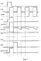
- Fig. 5 illustrates the timing chart for the signals at respective signal terminals, the PU node and the PD-CN node in the first stage of shift register unit, and the signals at the respective signal terminals in the first stage of outputting unit, with respect to a process during which the first stage of shift register unit finishes a shift once. It can be seen from the figure that an output signal 'gate1-out' of the first stage of gate driving unit may be maintained to be consistent with the output signal OUTPUT of the shift register completely.
- the output signal from the related shift register is abnormal accordingly, such that the output signals from other stages of shift registers are affected to be abnormal, which in turn lead to an abnormality in the signals of corresponding gate lines.
- the thin film transistors for driving the display which are connected to these gate lines, cannot operate normally, thereby causing an abnormal display in the full screen finally.
- the gate driving apparatus when a gate line is short-circuited with other wirings at a certain position in a liquid crystal display region, only the low level signal VSS and the high level signal Vgh may be affected, but driving abilities of the low level signal VSS and the high level signal Vgh are both strong and not easy to be pulled generally.
- the gate line short-circuited since the signals from the output terminal of the shift register is not connected to the gate line directly, the gate line short-circuited may not affect the output of the corresponding shift register, which in turn provide normally a normal reset signal to the (n-1) th stage of shift register unit and provide a normal input signal to the (n+1) th stage of shift register unit.
- driving timings and operation states of the gate driving unit may not be disordered and the liquid crystal display device may display normally the remaining regions except for the region(s) affected by the short-circuit.
- the abnormality in the full screen display caused by the short-circuit within the panel may be found easily and there are many methods for repairing the short-circuit within the panel of the liquid crystal display device so that a defective product can become a good product by repairing, which improves the product yield.
- the above embodiments are described only with respect to the shift register unit in a manner of gate driving using a pair of clock signals (CLK and CLKB), but they are not limited to the shift register unit in such a driving manner.
- the gate driving apparatus according to the embodiments of the present disclosure is also applicable, wherein the connection mode of the respective signal terminals of the outputting unit is the same as that of the embodiments of the present disclosure, and the details are omitted herein.
- the embodiments of the present disclosure provide a display device comprising the above gate driving apparatus.
- the embodiments of the present disclosure is able to settle the abnormal display in the full screen caused by an abnormality in signals output from the shift register, when a short-circuit occurs in wirings associated with gate lines within a liquid crystal panel, by arranging the outputting unit at the output terminal of the shift register unit, making an output signal from the shift register unit of the gate driving apparatus as a pulling-up control signal of the outputting unit, and providing an output signal to the gate line by the outputting unit, while it is able to enhance the efficiency of analysis for defective phenomena such as the abnormal display etc., and increase the product yield.
Landscapes
- Engineering & Computer Science (AREA)
- Chemical & Material Sciences (AREA)
- Crystallography & Structural Chemistry (AREA)
- Physics & Mathematics (AREA)
- Computer Hardware Design (AREA)
- General Physics & Mathematics (AREA)
- Theoretical Computer Science (AREA)
- Control Of Indicators Other Than Cathode Ray Tubes (AREA)
- Liquid Crystal Display Device Control (AREA)
- Shift Register Type Memory (AREA)
Description
- The present disclosure relates to a field of liquid crystal displaying technique, and particularly, to a gate driving apparatus and a display device.
- Application of a liquid crystal display device has filled in everywhere in people's life, such as a mobile phone, a game machine, a computer display, a television and the like. A traditional liquid crystal display device drives a liquid crystal panel to display generally in a manner of bonding by a gate driving IC and a source driving IC, and a driving technique for disposing a gate driver on the liquid crystal display integrally (gate in panel, GIP) arises to meet requirements for an increased resolution and a competitive cost pressure. In this technique, a gate driving circuit is composed of a plurality of thin film transistors TFTs, its manufacture process is the same as the liquid crystal display, which can reduce expenses of using the gate driving IC without increasing process difficulty and the cost.
-
Fig.1 is a schematic diagram illustrating a liquid crystal display driven by the existing GIP technique. A gate driving apparatus is composed of a plurality ofshift register units 1 connected in cascade, each of the shift register units corresponds to a gate driving signal line, wherein a STV (frame start signal) provides a start signal with a cycle being same as a frame frequency to the shiftregister unit S 1; a first clock signal CLK and a second clock signal CLKB are the same but have opposite polarities, and are used for controlling the shift register to output a high level signal or a low level signal. A low level maintaining signal is provided to the shift register by VSS. An output signal from the shift register unit S1 is as a start signal for a next shift register unit S2 and provides a reset signal to the shift register unit S1 at the same time when the shift register unit S2 outputs a high level, so that the output from theS 1 is at the low level to produce a progressive driving process of the liquid crystal display device. -
CN 102 708 925 A discloses a TFT shift register which comprises a shift register functional part and an auxiliary part, the shift register functional part is used for realizing a shift register function, the auxiliary part is used for controlling the voltage of a pulling low point in the shift register functional part, assisting charge and discharge of a PU point and an output terminal, and controlling output noise. - However, since the output signal from the shift register is connected directly with the gate driving signal line, the signal output from the shift register may change abnormally when a short-circuit occurs in the wirings associated with the gate driving signal lines (for example, a gate signal line and a data signal line, the gate signal line and a common electrode line) within the panel of the liquid crystal display device, which may affect visibly the resetting of the previous shift register and the turning-on of the next shift register and in turn cause a disorder in timings and operation states of all of the shift registers, such that a display in a full screen is abnormal or fails. This problem may also affect seriously the research and analysis of reasons for the defect of the abnormality in a picture displaying, which will be made by engineers, and it is not benefit for increasing the product yield.
- It is an object of the present disclosure to provide a gate driving apparatus and a display device to settle an abnormal display in a full screen caused by an abnormality in signals output from a shift register, when a short-circuit occurs in wirings associated with gate lines within a liquid crystal panel.
- The object is solved by the features of the respective independent claims. Further embodiments and developments are defined in the respective dependent claims.
- The gate driving apparatus according to the embodiments of the present disclosure comprises the features of
claim 1. - A display device according to the embodiments of the present disclosure comprises the above gate driving apparatus.
- The embodiments of the present disclosure may settle an abnormal display in a full screen caused by an abnormality in signals output from a shift register, when a short-circuit occurs in wirings associated with gate lines within a liquid crystal panel, by arranging the outputting unit at the output terminal of the shift register unit, making an output signal from the shift register unit of the gate driving apparatus as a pulling-up control signal of the outputting unit, and providing an output signal to the gate line by the outputting unit, while it is able to enhance an analysis efficiency for defective phenomena such as the normal display, etc, and increase the product yield.
-
-
Fig.1 is a schematic diagram illustrating a structure of a gate driving apparatus in the prior art; -
Fig.2 is a schematic diagram illustrating a structure of a gate driving apparatus according to an embodiment of the present disclosure; -
Fig.3 is a schematic diagram illustrating a structure of a shift register unit in the gate driving apparatus shown inFig. 1 ; -
Fig.4 is a schematic diagram illustrating a structure of an outputting unit according to an embodiment of the present disclosure; -
Fig.5 is a timing chart for respective signal terminals of the gate driving unit according to the embodiments of the present disclosure. - Embodiments of the present disclosure provide a gate driving apparatus and a display device for settling an abnormal displaying in a full screen caused by an abnormality in signals output from a shift register when short-circuit occurs in wirings associated with gate lines within a liquid crystal panel.
- The embodiments of the present disclosure will be described below in connection with drawings.
- Referring to
Fig.2 , the gate driving apparatus according to an embodiment of the present disclosure comprises a plurality ofgate driving units 2 connected in cascade, wherein each stage of thegate driving unit 2 comprises a shift register unit 3, for example, S1, S2, etc. inFig. 2 . The shift register unit 3 comprises a pulling-down control node PD-CN. Each stage of thegate driving unit 2 further comprises anoutputting unit 4, for example, Z1, Z2 and the like in the figure, for outputting a first power voltage Vgh or a second power voltage VSS to a gate line. - A pulling-up control terminal IN of the outputting unit is connected to an output terminal OUTPUT of the shift register unit, a reset signal terminal RET thereof is connected to a reset signal terminal RET of the shift register unit in the same stage of the gate driving unit, a pulling-down control terminal thereof is connected to a pulling-down control node PD-CN of the shift register unit in the same stage of the gate driving unit, a first power supply input terminal thereof is connected to the first power voltage Vgh, a second power supply input terminal thereof is connected to the second power voltage VSS, and an output terminal OUT of the outputting unit is connected to the gate line 'gate' as an output terminal of the gate driving unit.
- The
outputting unit 4 comprises: - a first outputting module for providing the first power voltage to the output terminal of the outputting unit, that is, outputting the same to the gate line, in response to a pulling-up control signal, namely in response to an output signal of the shift register unit;
- a second outputting module for providing the second power voltage to the output terminal of the outputting unit, in response to a reset signal;
- a third outputting module for providing the second power voltage to the output terminal of the outputting unit, in response to a pulling-down control signal, namely in response to a voltage signal at the PD-CN node of the shift register unit.
- Optionally, the first outputting module comprises a first thin film transistor with a gate connected to the pulling-up control terminal of the outputting unit, a source connected to the first power supply input terminal, and a drain connected to the output terminal of the outputting unit.
- Optionally, the second outputting module comprises a second thin film transistor with a gate connected to the reset signal terminal of the outputting unit, a source connected to the output terminal of the outputting unit, and a drain connected to the second power supply input terminal.
- Optionally, the third outputting module comprises a third thin film transistor with a gate connected to the pulling-down control terminal of the outputting unit, a source connected to the output terminal of the outputting unit, and a drain connected to the second power supply input terminal.
- Optionally, the shift register unit comprises a plurality of N-type thin film transistors, and the first thin film transistor, the second thin film transistor and the third thin film transistor in the outputting unit are all the N-type thin film transistors. The N-type thin film transistor is turned on at a high level and is turned off at a low level.
- Optionally, for the shift register units,
an input signal terminal of a first stage of shift register unit is connected to a frame start signal, and a reset signal terminal of the first stage of shift register unit is connected to an output terminal of a second stage of shift register unit;
an input signal terminal of a last stage of shift register unit is connected to an output terminal of a previous stage of shift register unit, and a reset signal terminal of the last stage of shift register unit is connected to the frame start signal, or is connected to an outputting terminal of any stage of shift register unit except its previous stage of shift register unit or an output terminal of the outputting unit;
except the first stage of shift register unit and the last stage of shift register unit, the input signal terminals of the remaining respective stages of shift register units are connected to the output terminals of their corresponding previous stages of shift register units, and the reset signal terminals thereof are connected to the output terminals of the next stages of shift register units. - The embodiments of the present disclosure will be described below in connection with drawings.
- Referring to
Fig. 2 , the gate driving apparatus according to an embodiment of the present disclosure comprises a plurality ofgate driving units 2 connected in cascade, wherein each stage of thegate driving unit 2 comprises a shift register unit 3, for example, S1, S2, and the like in the figure, which comprises a pulling-down control node PD-CN, and each stage of the gate driving unit further comprises anoutputting unit 4, for example, Z1, Z2 and the like in the figure. - A pulling-up control terminal IN of the outputting unit is connected to an output terminal OUTPUT of the shift register unit, a reset signal terminal RET thereof is connected to a reset signal terminal RET of the shift register unit, a pulling-down control terminal thereof is connected to a pulling-down control node PD-CN of the shift register unit, a first power supply input terminal thereof is connected to the first power voltage Vgh, a second power supply input terminal thereof is connected to the second power voltage VSS, and an output terminal OUT of the outputting unit is connected to the gate line 'gate' as an output terminal of the gate driving unit.
- Herein, the first power voltage Vgh is a high level, and the second power voltage VSS is a low level. An input signal terminal IN of the first stage of shift register unit S1 is connected to a frame start signal STV, the reset signal terminal RET of the first stage of shift register unit S1 is connected to an output terminal OUTPUT of the second stage of shift register unit; an input signal terminal of the last stage of shift register unit is connected to an output terminal of its previous stage of shift register unit, and a reset signal terminal of the last stage of shift register unit is connected to the frame start signal, or is connected to an output terminal of any stage of shift register unit except its previous stage of shift register unit or an output terminal of an
outputting unit 4; except for the first stage of shift register unit and the last stage of shift register unit, the input signal terminals of the remaining respective stages of shift register units are connected to the output terminals of previous stages of shift register units, and the reset signal terminals thereof are connected to the output terminals of next stages of shift register units. - As illustrated in
Fig.2 , a STV, as the frame start signal, provides a driving start control signal to the shift register; CLK and CLKB are a first clock signal and a second clock signal, respectively, and control the shift register to output a high level signal and a low level signal, respectively; a VSS provides a low level maintaining signal to the shift register 3 and theoutputting unit 4; a Vgh provides a high level signal to a gate signal line through theoutputting unit 4; and a high level signal output from theoutputting unit 4 is controlled by an output signal from the shift register 3. Among the above signals, a pulse cycle of the STV is the same as a frame frequency of a display device, the CLK and the CLKB have the same signal pulses but opposite polarities, and the Vgh and the VSS are the high level signal and the low level signal, respectively. During a process of progressive driving, when a first gate driving unit outputs a high level, an output signal at the high level from the shift register unit S1 functions as an input signal of the shift register unit S2 in the second gate driving unit; when the second gate driving unit outputs a high level, the output signal at the high level from the shift register unit S2 functions as a reset signal of the shift register unit S1 and the outputting unit Z1 (which makes the output from the shift register unit S1 and the gate signal be at the low levels); and when the S1 and Z1 are reset to the low level, the shift register S1 outputs a PD-CN signal to the outputting unit Z1 so as to maintain the output terminal of the outputting unit Z1 at the low level. - Similarly, the gate signal lines corresponding to each of the gate driving units outputs progressively a high level to drive a liquid crystal panel to drive progressively the display. The gate driving apparatus is always maintained to output the low level outside periods of time during which it outputs the high level.
-
Fig. 3 is a schematic diagram illustrating a circuit structure of a shift register unit connected in cascade in the prior art. The shift register unit is used for the prior art shown inFig. 1 and also may be used for the structure of the gate driving apparatus according to the embodiment of the present disclosure illustrated inFig. 2 . As shown inFigure 3 , regions marked byreference numerals - As illustrated in
Fig. 3 , the pulling-updriving module 11 of the shift register unit comprises a TFT M1 with a gate and a source connected to a STV signal, and a drain connected to a PU node;
the pulling-up module 12 comprises a TFT M3 and a capacitor C1, a source of the M3 is connected to a first clock signal CLK, a gate thereof is connected to the PU node, and a drain thereof is connected to an output terminal OUTPUT; a first end of the capacitor C1 is connected to the PU node, and a second end thereof is connected to the output terminal OUTPUT;
the pulling-down controllingmodule 13 comprises a TFT M6 with a gate connected to the PU node, a drain connected to a VSS, and a source used as a PD-CN node;
the pulling-downmodule 14 comprises TFTs M2, M4, M5 and M8, wherein a source of the M2 is connected to the PU node, a gate thereof is connected to the PD-CN node, and a drain thereof is connected to the VSS; a source of the M4 is connected to the output terminal OUTPUT, a gate thereof is connected to the PD-CN node, and a drain thereof is connected to the VSS; a source and a gate of the M5 are connected to the second clock signal CLKB, and a drain thereof is connected to the PD-CN node; a source of the M8 is connected to the second clock signal CLKB, a gate thereof is connected to the PU node, and a drain thereof is connected to the PD-CN node;
theresetting module 15 comprises TFTs M7 and M9, wherein a source of the M7 is connected to the PU node, a gate thereof is connected to the reset signal terminal RET, and a drain thereof is connected to the VSS; a source of the M9 is connected to the output terminal OUTPUT, a gate thereof is connected to the reset signal terminal RET, and a drain thereof is connected to the VSS. - In the example, the pulling-up
driving module 11 receives the high level signal outputting from the previous stage as a start signal, so that a level at the PU node connected with the pulling-upmodule 12 rises and a level at the PD-CN node is pulled down; when the first clock signal CLK is at the high level, the TFT M3 is turned on, and the shift register unit outputs the high level; when an output from the next stage of shift register unit is the high level (the second clock signal CLKB is at the high level), the RET signal is at the high level, the M7 and M9 are turned on, so that the PU node and the output terminal OUTPUT are pulled down to a low level VSS, and the PD-CN node is pulled up to the high level at the same time; in subsequent high-low level switching processes of the CLKB, the high level at the PD-CN node retains the M2 and M4 to be turned on and maintains the PU node and the output terminal OUTPUT of the shift register to be at the low level. - In the
gate driving unit 2 according to the embodiments of the present disclosure, the outputtingunit 4 receives a voltage signal at the pulling-down node PD-CN outputting from the shift register unit 3, so that the output terminal OUT of theoutputting unit 4 retains a low level signal. -
Fig. 4 is a schematic diagram illustrating an internal structure of theoutputting unit 4 in the nth gate driving unit according to an embodiment of the present disclosure. As shown inFig. 4 , the outputtingunit 4 comprises: afirst outputting module 41 for providing the first power voltage Vgh to the output terminal OUT of this outputting unit, that is, outputting the same to the gate line, in response to a pulling-up control signal, namely in response to the output signal of the shift register unit; asecond outputting module 42 for providing the second power voltage VSS to the output terminal OUT of this outputting unit, in response to a reset signal RET; athird outputting module 43 for providing the second power voltage VSS to the output terminal of the outputting unit, in response to a pulling-down control signal PD-CN, namely in response to the voltage signal at the PD-CN node of the shift register unit. - Specifically, the first outputting module comprises a first thin film transistor M21 whose gate is connected to the pulling-up control terminal IN of the outputting unit, source is connected to the first power supply input terminal Vgh, and drain is connected to the output terminal OUT of the outputting unit.
- Specifically, the second outputting module comprises a second thin film transistor M22 whose gate is connected to the reset signal terminal RET of the outputting unit, source is connected to the output terminal OUT of the outputting unit, and drain is connected to the second power supply input terminal VSS.
- Specifically, the third outputting module comprises a third thin film transistor M23 whose gate is connected to the pulling-down control terminal PD-CN of the outputting unit, source is connected to the output terminal OUT of the outputting unit, and drain is connected to the second power supply input terminal VSS.
- In the gate driving apparatus according to the embodiments of the present disclosure, all of the thin film transistors in the above shift register unit are N-type thin film transistors, the first thin film transistor, the second thin film transistor and the third thin film transistor in the outputting unit are all the N-type thin film transistors. All of the N-type thin film transistors are turned on at a high level and are turned off at a low level.
- A detailed operation principle of the
outputting unit 4 is as follows. - When the shift register n outputs a high level, it shifts to a shift register n+1, at the same time the TFT M21 is turned on so that the output terminal OUT of the outputting unit outputs the high level Vgh to the gate line; when the shift register unit n outputs a low level, the TFT M21 is turned off, so that the output terminal OUT of the outputting unit is disconnected from Vgh.
- When the shift register n+1 outputs the high level, the RET signal is at the high level, the TFT M22 is turned on, so that the VSS signal pulls down the level at the output terminal OUT of the outputting unit n, and the gate signal line n is at the low level correspondingly; when the shift register n+1 is reset to the low level, the low level at the output terminal OUT of the outputting unit n cannot be maintained continually.
- At this time, the pulling-down control signal PD-CN of the shift register is high, so that the TFT M23 is turned on and the output terminal OUT of the
outputting unit 4 is retained to be the low level signal VSS. Thus, with timing signals output from the outputting unit, the signal on the gate line can be at the high level when the shift register outputs the high level, and the signal on the gate line can be maintained at the low level outside the periods of time during which the shift register outputs the high level, so that the signal on the gate line can be ensured to be consistent with the output signal from the shift register. - The embodiments of the present disclosure will be described more clearly by referring to a timing chart illustrated in
Fig. 5. Fig. 5 illustrates the timing chart for the signals at respective signal terminals, the PU node and the PD-CN node in the first stage of shift register unit, and the signals at the respective signal terminals in the first stage of outputting unit, with respect to a process during which the first stage of shift register unit finishes a shift once. It can be seen from the figure that an output signal 'gate1-out' of the first stage of gate driving unit may be maintained to be consistent with the output signal OUTPUT of the shift register completely. - In the gate driving apparatus of the prior art, when the gate line is short-circuited with other wirings at a certain position in a liquid crystal display region, the output signal from the related shift register is abnormal accordingly, such that the output signals from other stages of shift registers are affected to be abnormal, which in turn lead to an abnormality in the signals of corresponding gate lines. As a result, the thin film transistors for driving the display, which are connected to these gate lines, cannot operate normally, thereby causing an abnormal display in the full screen finally.
- However, in the gate driving apparatus according to the embodiments of the present disclosure, when a gate line is short-circuited with other wirings at a certain position in a liquid crystal display region, only the low level signal VSS and the high level signal Vgh may be affected, but driving abilities of the low level signal VSS and the high level signal Vgh are both strong and not easy to be pulled generally. Meanwhile, in the embodiments of the present disclosure, since the signals from the output terminal of the shift register is not connected to the gate line directly, the gate line short-circuited may not affect the output of the corresponding shift register, which in turn provide normally a normal reset signal to the (n-1)th stage of shift register unit and provide a normal input signal to the (n+1)th stage of shift register unit. Therefore, driving timings and operation states of the gate driving unit may not be disordered and the liquid crystal display device may display normally the remaining regions except for the region(s) affected by the short-circuit. Thus, the abnormality in the full screen display caused by the short-circuit within the panel may be found easily and there are many methods for repairing the short-circuit within the panel of the liquid crystal display device so that a defective product can become a good product by repairing, which improves the product yield.
- The above embodiments are described only with respect to the shift register unit in a manner of gate driving using a pair of clock signals (CLK and CLKB), but they are not limited to the shift register unit in such a driving manner. For example, for a shift register unit having many gate lines and using a driving manner with a plurality groups of clock signals, the gate driving apparatus according to the embodiments of the present disclosure is also applicable, wherein the connection mode of the respective signal terminals of the outputting unit is the same as that of the embodiments of the present disclosure, and the details are omitted herein.
- The embodiments of the present disclosure provide a display device comprising the above gate driving apparatus.
- In conclusion, the embodiments of the present disclosure is able to settle the abnormal display in the full screen caused by an abnormality in signals output from the shift register, when a short-circuit occurs in wirings associated with gate lines within a liquid crystal panel, by arranging the outputting unit at the output terminal of the shift register unit, making an output signal from the shift register unit of the gate driving apparatus as a pulling-up control signal of the outputting unit, and providing an output signal to the gate line by the outputting unit, while it is able to enhance the efficiency of analysis for defective phenomena such as the abnormal display etc., and increase the product yield.
- Obviously, those skilled in the art may make various amendments and variations to the embodiments of the present invention without departing from the scope of the present invention as defined in the appended claims. Thus, the present disclosure intends to cover such amendments and variations if they fall into the scope of the invention defined in the appended claims.
Claims (4)
- A gate driving apparatus comprising a plurality of gate driving units (2) connected in cascade, wherein each stage of the gate driving units (2) comprises a shift register unit (3) comprising a pulling-up driving module (11), a pulling-up module (12), a pulling-down controlling module (13), a pulling-down module (14), and a resetting module (15), wherein an input terminal of the pulling-down controlling module (13) is connected to a pulling-up node (PU), and an output terminal of the pulling-down controlling module (13) is connected to a pulling-down control node (PD-CN) in the pulling-down module (14),
characterized in that each stage of the gate driving units (2) further comprises an outputting unit (4) for outputting a first power voltage (Vgh) or a second power voltage (VSS) to a respective gate line (gate1, gate2, ...), the outputting unit (4) comprising:a first outputting module (41) with a pulling-up control terminal (IN) connected to an output terminal (OUTPUT) of the shift register unit (3), for providing the first power voltage (Vgh) to an output terminal (OUT) of the outputting unit (4), in response to an output signal of the shift register unit (3);a second outputting module (42) with a terminal connected to a reset signal terminal (RET) of the shift register unit (3), for providing the second power voltage (VSS) to the output terminal (OUT) of the outputting unit (4), in response to a reset signal;a third outputting module (43) with a pulling-down control terminal (PD-CN signal) connected to the pulling-down control node (PD-CN) of the shift register unit (3), for providing the second power voltage (VSS) to the output terminal (OUT) of the outputting unit (4), in response to a voltage signal at the pulling-down control node (PD-CN),wherein a first power supply input terminal of the outputting unit (4) is connected to the first power voltage (Vgh), a second power supply input terminal of the outputting unit (4) is connected to the second power voltage (VSS), and the output terminal (OUT) of the outputting unit (4) is connected to the respective gate line (gate1, gate2, ...) as an output terminal (OUT) of the gate driving unit, so that the output terminal (OUTPUT) of the shift register unit (3) is not directly connected to the respective gate line (gate1, gate2, ...) to avoid a gate line shorted-circuit from affecting an output of the corresponding shift register unit (3);wherein the first outputting module (41) comprises a first thin film transistor (M21) whose gate is connected to the pulling-up control terminal (IN) of the outputting unit (4), whose source is connected to the first power supply input terminal (Vgh), and whose drain is connected to the output terminal (OUT) of the outputting unit (4);wherein the second outputting module (42) comprises a second thin film transistor (M22) whose gate is connected to the reset signal terminal (RET) of the outputting unit (4), whose source is connected to the output terminal (OUT) of the outputting unit (4), and whose drain is connected to the second power supply input terminal (VSS);wherein the third outputting module (43) comprises a third thin film transistor (M23) whose gate is connected to the pulling-down control terminal (PD-CN signal) of the outputting unit (4), whose source is connected to the output terminal (OUT) of the outputting unit (4), and whose drain is connected to the second power supply input terminal (VSS),the pulling-up module (12) comprises a fourth thin film transistor (M3) and a capacitor (C1), a gate of the fourth thin film transistor (M3) is connected to the pulling-up node (PU) and a first end of the capacitor (C1), a source of the fourth thin film transistor (M3) is connected to a clock signal input terminal (CLK), and a drain of the fourth thin film transistor (M3) is connected to the output terminal (OUTPUT) of the shift register and a second end of the capacitor (C1);the pulling-down controlling module (13) comprises a fifth thin film transistor (M6), a gate of the fifth thin film transistor (M6) is connected to the pulling-up node (PU), a source of the fifth thin film transistor (M6) is connected to the pulling-down control node (PD-CN), and a drain of the fifth thin film transistor (M6) is connected to the second power voltage input terminal (VSS); andthe resetting module (15) comprises a sixth thin film transistor (M7) and a seventh thin film transistor (M9), a gate of the sixth thin film transistor (M7) is connected to the reset signal terminal (RET), a source of the sixth thin film transistor (M7) is connected to the pulling-up node (PU), and a drain of the sixth thin film transistor (M7) is connected to the second power voltage input terminal (VSS), and a gate of the seventh thin film transistor (M9) is connected to the reset signal terminal (RET), a source of the seventh thin film transistor (M9) is connected to the output terminal (OUTPUT) of the shift register, and a drain of the seventh thin film transistor (M9) is connected to the second power voltage input terminal (VSS). - The gate driving apparatus of claim 1, characterized in that all of the thin film transistors (M21, M22, M23, M3, M6, M7, M9) are N-type thin film transistors.
- The gate driving apparatus of claim 1, characterized in that
an input signal terminal (IN) of a first stage of shift register unit (S1) is connected to a frame start signal (STV), and a reset signal terminal (RET) of the first stage of shift register unit (S1) is connected to an output terminal (OUTPUT) of a second stage of shift register unit (S2);
an input signal terminal of a last stage of shift register unit is connected to an output terminal of a previous stage of shift register unit, and a reset signal terminal of the last stage of shift register unit is connected to the frame start signal (STV), or is connected to an output terminal of any stage of the shift register units except for its previous stage of shift register unit or an output terminal of an outputting unit;
except for the first stage of shift register unit (S1) and the last stage of shift register unit, the input signal terminals of the remaining respective stage of shift register units are connected to the output terminals of their previous stage of shift register unit, and the reset signal terminals thereof are connected to the output terminals of next stage of shift register unit. - A display device, characterized in that the display device comprises the gate driving apparatus of any one of claims 1 to 3.
Applications Claiming Priority (1)
| Application Number | Priority Date | Filing Date | Title |
|---|---|---|---|
| CN201210500711.6A CN103000151B (en) | 2012-11-29 | 2012-11-29 | Gate drive device and display device |
Publications (2)
| Publication Number | Publication Date |
|---|---|
| EP2738758A1 EP2738758A1 (en) | 2014-06-04 |
| EP2738758B1 true EP2738758B1 (en) | 2018-04-11 |
Family
ID=47928651
Family Applications (1)
| Application Number | Title | Priority Date | Filing Date |
|---|---|---|---|
| EP13194861.4A Not-in-force EP2738758B1 (en) | 2012-11-29 | 2013-11-28 | Gate driving apparatus and display device |
Country Status (3)
| Country | Link |
|---|---|
| US (1) | US9570025B2 (en) |
| EP (1) | EP2738758B1 (en) |
| CN (1) | CN103000151B (en) |
Families Citing this family (18)
| Publication number | Priority date | Publication date | Assignee | Title |
|---|---|---|---|---|
| CN103247276B (en) * | 2013-04-25 | 2015-03-18 | 北京京东方光电科技有限公司 | Gate drive circuit and array substrate |
| CN103489483A (en) * | 2013-09-02 | 2014-01-01 | 合肥京东方光电科技有限公司 | Shift register unit circuit, shift register, array substrate and display device |
| CN103943081A (en) * | 2014-03-14 | 2014-07-23 | 京东方科技集团股份有限公司 | Shifting register, manufacturing method of shifting register, grid line integrated drive circuit and relevant devices |
| CN104036714B (en) * | 2014-05-26 | 2017-02-01 | 京东方科技集团股份有限公司 | GOA circuit, display substrate and display device |
| CN104282287B (en) | 2014-10-31 | 2017-03-08 | 合肥鑫晟光电科技有限公司 | A kind of GOA unit and driving method, GOA circuit and display device |
| CN108573668B (en) * | 2017-03-10 | 2021-05-18 | 京东方科技集团股份有限公司 | Shift register unit and driving method thereof, gate driving circuit and display device |
| US20210280108A1 (en) * | 2017-05-15 | 2021-09-09 | Shenzhen Royole Technologies Co., Ltd. | Goa circuit, array substrate, and display device |
| CN107516498A (en) * | 2017-09-28 | 2017-12-26 | 惠科股份有限公司 | Driving device and driving method of display device |
| CN107863074B (en) * | 2017-10-30 | 2018-10-09 | 南京中电熊猫液晶显示科技有限公司 | Gated sweep driving circuit |
| CN108172170B (en) * | 2017-11-30 | 2019-12-13 | 南京中电熊猫平板显示科技有限公司 | A trigger driving circuit and an organic light-emitting display device |
| CN110322847B (en) | 2018-03-30 | 2021-01-22 | 京东方科技集团股份有限公司 | Gate drive circuit, display device and drive method |
| CN108766357B (en) * | 2018-05-31 | 2020-04-03 | 京东方科技集团股份有限公司 | Signal combining circuit, gate driving unit, gate driving circuit and display device |
| CN108777128A (en) * | 2018-05-31 | 2018-11-09 | 京东方科技集团股份有限公司 | Shift register and its driving method, gate driving circuit and display device |
| CN111312136B (en) * | 2018-12-12 | 2022-01-14 | 京东方科技集团股份有限公司 | Shift register unit, scanning driving circuit, driving method and display device |
| CN109979373B (en) * | 2019-05-07 | 2023-08-08 | 京东方科技集团股份有限公司 | Shift register unit, shift register, display device and test method thereof |
| JP7347054B2 (en) * | 2019-09-17 | 2023-09-20 | 富士電機株式会社 | Status output circuit and power supply device |
| CN116631353B (en) * | 2023-05-31 | 2025-12-23 | 绵阳惠科光电科技有限公司 | Pixel unit driving circuit, array substrate, display panel and display |
| CN117037670A (en) * | 2023-08-25 | 2023-11-10 | 北京奕斯伟计算技术股份有限公司 | A gate drive circuit and display device |
Family Cites Families (19)
| Publication number | Priority date | Publication date | Assignee | Title |
|---|---|---|---|---|
| KR100788391B1 (en) * | 2001-02-27 | 2007-12-31 | 엘지.필립스 엘시디 주식회사 | Bidirectional driving circuit of liquid crystal display panel |
| US7050036B2 (en) * | 2001-12-12 | 2006-05-23 | Lg.Philips Lcd Co., Ltd. | Shift register with a built in level shifter |
| KR20050117303A (en) * | 2004-06-10 | 2005-12-14 | 삼성전자주식회사 | Display device |
| US7529333B2 (en) * | 2005-10-27 | 2009-05-05 | Lg Display Co., Ltd. | Shift register |
| KR101275248B1 (en) * | 2006-06-12 | 2013-06-14 | 삼성디스플레이 주식회사 | Gate driver circuit and display apparatus having the same |
| US7936332B2 (en) * | 2006-06-21 | 2011-05-03 | Samsung Electronics Co., Ltd. | Gate driving circuit having reduced ripple effect and display apparatus having the same |
| KR101192799B1 (en) * | 2006-10-19 | 2012-10-18 | 엘지디스플레이 주식회사 | Shift register |
| GB2452279A (en) | 2007-08-30 | 2009-03-04 | Sharp Kk | An LCD scan pulse shift register stage with a gate line driver and a separate logic output buffer |
| KR100911982B1 (en) * | 2008-03-04 | 2009-08-13 | 삼성모바일디스플레이주식회사 | Emission driver and organic light emitting display device using same |
| CN101546607B (en) | 2008-03-26 | 2012-02-29 | 北京京东方光电科技有限公司 | Shift register and grid driving device for liquid crystal display |
| CN102012591B (en) * | 2009-09-04 | 2012-05-30 | 北京京东方光电科技有限公司 | Shift register unit and liquid crystal display gate drive device |
| US9373414B2 (en) * | 2009-09-10 | 2016-06-21 | Beijing Boe Optoelectronics Technology Co., Ltd. | Shift register unit and gate drive device for liquid crystal display |
| CN102024500B (en) * | 2009-09-10 | 2013-03-27 | 北京京东方光电科技有限公司 | Shift register unit and actuating device for gate of liquid crystal display |
| CN102110420B (en) * | 2009-12-24 | 2013-07-10 | 北京京东方光电科技有限公司 | Array substrate and shift register arranged thereon |
| KR101739575B1 (en) * | 2010-09-28 | 2017-05-25 | 삼성디스플레이 주식회사 | Apparatus of scan driving and driving method thereof |
| CN102467891B (en) * | 2010-10-29 | 2013-10-09 | 京东方科技集团股份有限公司 | Shift register unit, gate driving device and liquid crystal display |
| CN102651238B (en) * | 2011-04-18 | 2015-03-25 | 京东方科技集团股份有限公司 | Shift register unit, shift register, display panel and display |
| CN102708925B (en) * | 2011-05-26 | 2015-08-12 | 京东方科技集团股份有限公司 | Shift register for thin-film transistor and application process thereof |
| CN103065578B (en) * | 2012-12-13 | 2015-05-13 | 京东方科技集团股份有限公司 | Shifting register unit and grid drive circuit and display device |
-
2012
- 2012-11-29 CN CN201210500711.6A patent/CN103000151B/en not_active Expired - Fee Related
-
2013
- 2013-11-27 US US14/092,497 patent/US9570025B2/en not_active Expired - Fee Related
- 2013-11-28 EP EP13194861.4A patent/EP2738758B1/en not_active Not-in-force
Non-Patent Citations (1)
| Title |
|---|
| None * |
Also Published As
| Publication number | Publication date |
|---|---|
| US9570025B2 (en) | 2017-02-14 |
| CN103000151B (en) | 2014-09-10 |
| EP2738758A1 (en) | 2014-06-04 |
| CN103000151A (en) | 2013-03-27 |
| US20140145924A1 (en) | 2014-05-29 |
Similar Documents
| Publication | Publication Date | Title |
|---|---|---|
| US9570025B2 (en) | Gate driving apparatus and display device | |
| US9269455B2 (en) | Shift register unit, gate driving circuit, array substrate and display apparatus | |
| US10217428B2 (en) | Output control unit for shift register, shift register and driving method thereof, and gate driving device | |
| US9886927B2 (en) | Display device, TFT substrate and GOA driving circuit | |
| US9881543B2 (en) | Shift register unit, method for driving the same, shift register, and display device | |
| US9886921B2 (en) | Gate driving circuit, gate driving method, and liquid crystal display | |
| US9632611B1 (en) | GOA circuit for in-cell type touch display panel | |
| US9240781B2 (en) | Shift register, display apparatus, gate driving circuit, and driving method | |
| EP3133583B1 (en) | Shift register unit, driving method therefor, shift register circuit, and display device | |
| US9558843B2 (en) | Shift register unit, gate driving circuit, and display device comprising the same | |
| US20130088265A1 (en) | Gate driver on array, shifting regester and display screen | |
| US10698526B2 (en) | Compensation circuit, gate driving unit, gate driving circuit, driving methods thereof and display device | |
| US20070086558A1 (en) | Gate line drivers for active matrix displays | |
| WO2017117849A1 (en) | Goa drive circuit | |
| US20180374442A1 (en) | Goa circuit driving architecture | |
| WO2019134221A1 (en) | Goa circuit | |
| WO2016070543A1 (en) | Shift register unit, gate driving circuit and display device | |
| US9478171B2 (en) | Display device and method for operating the display device | |
| US20160125847A1 (en) | Goa unit and method for driving the same, goa circuit and display device | |
| JP2010061130A (en) | Gate driving circuit | |
| US9495929B2 (en) | Shift register, driver circuit and display device | |
| CN103915052A (en) | Grid driving circuit and method and display device | |
| JP2019502148A (en) | GOA drive circuit, TFT display panel and display device | |
| JP6555842B2 (en) | GOA circuit, driving method thereof, and liquid crystal display | |
| TWI618043B (en) | Gate driving circuit, driving method thereof and flat display device |
Legal Events
| Date | Code | Title | Description |
|---|---|---|---|
| PUAI | Public reference made under article 153(3) epc to a published international application that has entered the european phase |
Free format text: ORIGINAL CODE: 0009012 |
|
| 17P | Request for examination filed |
Effective date: 20131128 |
|
| AK | Designated contracting states |
Kind code of ref document: A1 Designated state(s): AL AT BE BG CH CY CZ DE DK EE ES FI FR GB GR HR HU IE IS IT LI LT LU LV MC MK MT NL NO PL PT RO RS SE SI SK SM TR |
|
| AX | Request for extension of the european patent |
Extension state: BA ME |
|
| R17P | Request for examination filed (corrected) |
Effective date: 20141113 |
|
| RBV | Designated contracting states (corrected) |
Designated state(s): AL AT BE BG CH CY CZ DE DK EE ES FI FR GB GR HR HU IE IS IT LI LT LU LV MC MK MT NL NO PL PT RO RS SE SI SK SM TR |
|
| 17Q | First examination report despatched |
Effective date: 20160908 |
|
| STAA | Information on the status of an ep patent application or granted ep patent |
Free format text: STATUS: EXAMINATION IS IN PROGRESS |
|
| GRAP | Despatch of communication of intention to grant a patent |
Free format text: ORIGINAL CODE: EPIDOSNIGR1 |
|
| STAA | Information on the status of an ep patent application or granted ep patent |
Free format text: STATUS: GRANT OF PATENT IS INTENDED |
|
| INTG | Intention to grant announced |
Effective date: 20171027 |
|
| GRAS | Grant fee paid |
Free format text: ORIGINAL CODE: EPIDOSNIGR3 |
|
| GRAA | (expected) grant |
Free format text: ORIGINAL CODE: 0009210 |
|
| STAA | Information on the status of an ep patent application or granted ep patent |
Free format text: STATUS: THE PATENT HAS BEEN GRANTED |
|
| AK | Designated contracting states |
Kind code of ref document: B1 Designated state(s): AL AT BE BG CH CY CZ DE DK EE ES FI FR GB GR HR HU IE IS IT LI LT LU LV MC MK MT NL NO PL PT RO RS SE SI SK SM TR |
|
| REG | Reference to a national code |
Ref country code: GB Ref legal event code: FG4D |
|
| REG | Reference to a national code |
Ref country code: CH Ref legal event code: EP |
|
| REG | Reference to a national code |
Ref country code: AT Ref legal event code: REF Ref document number: 988820 Country of ref document: AT Kind code of ref document: T Effective date: 20180415 |
|
| REG | Reference to a national code |
Ref country code: IE Ref legal event code: FG4D |
|
| REG | Reference to a national code |
Ref country code: DE Ref legal event code: R096 Ref document number: 602013035655 Country of ref document: DE |
|
| REG | Reference to a national code |
Ref country code: NL Ref legal event code: FP |
|
| REG | Reference to a national code |
Ref country code: LT Ref legal event code: MG4D |
|
| REG | Reference to a national code |
Ref country code: FR Ref legal event code: PLFP Year of fee payment: 6 |
|
| PG25 | Lapsed in a contracting state [announced via postgrant information from national office to epo] |
Ref country code: ES Free format text: LAPSE BECAUSE OF FAILURE TO SUBMIT A TRANSLATION OF THE DESCRIPTION OR TO PAY THE FEE WITHIN THE PRESCRIBED TIME-LIMIT Effective date: 20180411 Ref country code: AL Free format text: LAPSE BECAUSE OF FAILURE TO SUBMIT A TRANSLATION OF THE DESCRIPTION OR TO PAY THE FEE WITHIN THE PRESCRIBED TIME-LIMIT Effective date: 20180411 Ref country code: LT Free format text: LAPSE BECAUSE OF FAILURE TO SUBMIT A TRANSLATION OF THE DESCRIPTION OR TO PAY THE FEE WITHIN THE PRESCRIBED TIME-LIMIT Effective date: 20180411 Ref country code: NO Free format text: LAPSE BECAUSE OF FAILURE TO SUBMIT A TRANSLATION OF THE DESCRIPTION OR TO PAY THE FEE WITHIN THE PRESCRIBED TIME-LIMIT Effective date: 20180711 Ref country code: FI Free format text: LAPSE BECAUSE OF FAILURE TO SUBMIT A TRANSLATION OF THE DESCRIPTION OR TO PAY THE FEE WITHIN THE PRESCRIBED TIME-LIMIT Effective date: 20180411 Ref country code: BG Free format text: LAPSE BECAUSE OF FAILURE TO SUBMIT A TRANSLATION OF THE DESCRIPTION OR TO PAY THE FEE WITHIN THE PRESCRIBED TIME-LIMIT Effective date: 20180711 Ref country code: PL Free format text: LAPSE BECAUSE OF FAILURE TO SUBMIT A TRANSLATION OF THE DESCRIPTION OR TO PAY THE FEE WITHIN THE PRESCRIBED TIME-LIMIT Effective date: 20180411 Ref country code: SE Free format text: LAPSE BECAUSE OF FAILURE TO SUBMIT A TRANSLATION OF THE DESCRIPTION OR TO PAY THE FEE WITHIN THE PRESCRIBED TIME-LIMIT Effective date: 20180411 |
|
| PG25 | Lapsed in a contracting state [announced via postgrant information from national office to epo] |
Ref country code: GR Free format text: LAPSE BECAUSE OF FAILURE TO SUBMIT A TRANSLATION OF THE DESCRIPTION OR TO PAY THE FEE WITHIN THE PRESCRIBED TIME-LIMIT Effective date: 20180712 Ref country code: RS Free format text: LAPSE BECAUSE OF FAILURE TO SUBMIT A TRANSLATION OF THE DESCRIPTION OR TO PAY THE FEE WITHIN THE PRESCRIBED TIME-LIMIT Effective date: 20180411 Ref country code: LV Free format text: LAPSE BECAUSE OF FAILURE TO SUBMIT A TRANSLATION OF THE DESCRIPTION OR TO PAY THE FEE WITHIN THE PRESCRIBED TIME-LIMIT Effective date: 20180411 Ref country code: HR Free format text: LAPSE BECAUSE OF FAILURE TO SUBMIT A TRANSLATION OF THE DESCRIPTION OR TO PAY THE FEE WITHIN THE PRESCRIBED TIME-LIMIT Effective date: 20180411 |
|
| REG | Reference to a national code |
Ref country code: AT Ref legal event code: MK05 Ref document number: 988820 Country of ref document: AT Kind code of ref document: T Effective date: 20180411 |
|
| PG25 | Lapsed in a contracting state [announced via postgrant information from national office to epo] |
Ref country code: PT Free format text: LAPSE BECAUSE OF FAILURE TO SUBMIT A TRANSLATION OF THE DESCRIPTION OR TO PAY THE FEE WITHIN THE PRESCRIBED TIME-LIMIT Effective date: 20180813 |
|
| REG | Reference to a national code |
Ref country code: DE Ref legal event code: R097 Ref document number: 602013035655 Country of ref document: DE |
|
| PG25 | Lapsed in a contracting state [announced via postgrant information from national office to epo] |
Ref country code: CZ Free format text: LAPSE BECAUSE OF FAILURE TO SUBMIT A TRANSLATION OF THE DESCRIPTION OR TO PAY THE FEE WITHIN THE PRESCRIBED TIME-LIMIT Effective date: 20180411 Ref country code: RO Free format text: LAPSE BECAUSE OF FAILURE TO SUBMIT A TRANSLATION OF THE DESCRIPTION OR TO PAY THE FEE WITHIN THE PRESCRIBED TIME-LIMIT Effective date: 20180411 Ref country code: SK Free format text: LAPSE BECAUSE OF FAILURE TO SUBMIT A TRANSLATION OF THE DESCRIPTION OR TO PAY THE FEE WITHIN THE PRESCRIBED TIME-LIMIT Effective date: 20180411 Ref country code: DK Free format text: LAPSE BECAUSE OF FAILURE TO SUBMIT A TRANSLATION OF THE DESCRIPTION OR TO PAY THE FEE WITHIN THE PRESCRIBED TIME-LIMIT Effective date: 20180411 Ref country code: EE Free format text: LAPSE BECAUSE OF FAILURE TO SUBMIT A TRANSLATION OF THE DESCRIPTION OR TO PAY THE FEE WITHIN THE PRESCRIBED TIME-LIMIT Effective date: 20180411 Ref country code: AT Free format text: LAPSE BECAUSE OF FAILURE TO SUBMIT A TRANSLATION OF THE DESCRIPTION OR TO PAY THE FEE WITHIN THE PRESCRIBED TIME-LIMIT Effective date: 20180411 |
|
| PLBE | No opposition filed within time limit |
Free format text: ORIGINAL CODE: 0009261 |
|
| STAA | Information on the status of an ep patent application or granted ep patent |
Free format text: STATUS: NO OPPOSITION FILED WITHIN TIME LIMIT |
|
| PG25 | Lapsed in a contracting state [announced via postgrant information from national office to epo] |
Ref country code: IT Free format text: LAPSE BECAUSE OF FAILURE TO SUBMIT A TRANSLATION OF THE DESCRIPTION OR TO PAY THE FEE WITHIN THE PRESCRIBED TIME-LIMIT Effective date: 20180411 Ref country code: SM Free format text: LAPSE BECAUSE OF FAILURE TO SUBMIT A TRANSLATION OF THE DESCRIPTION OR TO PAY THE FEE WITHIN THE PRESCRIBED TIME-LIMIT Effective date: 20180411 |
|
| 26N | No opposition filed |
Effective date: 20190114 |
|
| PG25 | Lapsed in a contracting state [announced via postgrant information from national office to epo] |
Ref country code: SI Free format text: LAPSE BECAUSE OF FAILURE TO SUBMIT A TRANSLATION OF THE DESCRIPTION OR TO PAY THE FEE WITHIN THE PRESCRIBED TIME-LIMIT Effective date: 20180411 |
|
| REG | Reference to a national code |
Ref country code: CH Ref legal event code: PL |
|
| PG25 | Lapsed in a contracting state [announced via postgrant information from national office to epo] |
Ref country code: LU Free format text: LAPSE BECAUSE OF NON-PAYMENT OF DUE FEES Effective date: 20181128 Ref country code: MC Free format text: LAPSE BECAUSE OF FAILURE TO SUBMIT A TRANSLATION OF THE DESCRIPTION OR TO PAY THE FEE WITHIN THE PRESCRIBED TIME-LIMIT Effective date: 20180411 |
|
| REG | Reference to a national code |
Ref country code: BE Ref legal event code: MM Effective date: 20181130 |
|
| REG | Reference to a national code |
Ref country code: IE Ref legal event code: MM4A |
|
| PG25 | Lapsed in a contracting state [announced via postgrant information from national office to epo] |
Ref country code: CH Free format text: LAPSE BECAUSE OF NON-PAYMENT OF DUE FEES Effective date: 20181130 Ref country code: LI Free format text: LAPSE BECAUSE OF NON-PAYMENT OF DUE FEES Effective date: 20181130 |
|
| PG25 | Lapsed in a contracting state [announced via postgrant information from national office to epo] |
Ref country code: IE Free format text: LAPSE BECAUSE OF NON-PAYMENT OF DUE FEES Effective date: 20181128 |
|
| PG25 | Lapsed in a contracting state [announced via postgrant information from national office to epo] |
Ref country code: BE Free format text: LAPSE BECAUSE OF NON-PAYMENT OF DUE FEES Effective date: 20181130 |
|
| PG25 | Lapsed in a contracting state [announced via postgrant information from national office to epo] |
Ref country code: MT Free format text: LAPSE BECAUSE OF NON-PAYMENT OF DUE FEES Effective date: 20181128 |
|
| PG25 | Lapsed in a contracting state [announced via postgrant information from national office to epo] |
Ref country code: TR Free format text: LAPSE BECAUSE OF FAILURE TO SUBMIT A TRANSLATION OF THE DESCRIPTION OR TO PAY THE FEE WITHIN THE PRESCRIBED TIME-LIMIT Effective date: 20180411 |
|
| PG25 | Lapsed in a contracting state [announced via postgrant information from national office to epo] |
Ref country code: MK Free format text: LAPSE BECAUSE OF NON-PAYMENT OF DUE FEES Effective date: 20180411 Ref country code: HU Free format text: LAPSE BECAUSE OF FAILURE TO SUBMIT A TRANSLATION OF THE DESCRIPTION OR TO PAY THE FEE WITHIN THE PRESCRIBED TIME-LIMIT; INVALID AB INITIO Effective date: 20131128 Ref country code: CY Free format text: LAPSE BECAUSE OF FAILURE TO SUBMIT A TRANSLATION OF THE DESCRIPTION OR TO PAY THE FEE WITHIN THE PRESCRIBED TIME-LIMIT Effective date: 20180411 |
|
| PG25 | Lapsed in a contracting state [announced via postgrant information from national office to epo] |
Ref country code: IS Free format text: LAPSE BECAUSE OF FAILURE TO SUBMIT A TRANSLATION OF THE DESCRIPTION OR TO PAY THE FEE WITHIN THE PRESCRIBED TIME-LIMIT Effective date: 20180811 |
|
| PGFP | Annual fee paid to national office [announced via postgrant information from national office to epo] |
Ref country code: FR Payment date: 20211109 Year of fee payment: 9 Ref country code: GB Payment date: 20211007 Year of fee payment: 9 |
|
| PGFP | Annual fee paid to national office [announced via postgrant information from national office to epo] |
Ref country code: NL Payment date: 20221118 Year of fee payment: 10 Ref country code: DE Payment date: 20221121 Year of fee payment: 10 |
|
| GBPC | Gb: european patent ceased through non-payment of renewal fee |
Effective date: 20221128 |
|
| PG25 | Lapsed in a contracting state [announced via postgrant information from national office to epo] |
Ref country code: GB Free format text: LAPSE BECAUSE OF NON-PAYMENT OF DUE FEES Effective date: 20221128 |
|
| PG25 | Lapsed in a contracting state [announced via postgrant information from national office to epo] |
Ref country code: FR Free format text: LAPSE BECAUSE OF NON-PAYMENT OF DUE FEES Effective date: 20221130 |
|
| REG | Reference to a national code |
Ref country code: DE Ref legal event code: R119 Ref document number: 602013035655 Country of ref document: DE |
|
| REG | Reference to a national code |
Ref country code: NL Ref legal event code: MM Effective date: 20231201 |
|
| PG25 | Lapsed in a contracting state [announced via postgrant information from national office to epo] |
Ref country code: NL Free format text: LAPSE BECAUSE OF NON-PAYMENT OF DUE FEES Effective date: 20231201 |
|
| PG25 | Lapsed in a contracting state [announced via postgrant information from national office to epo] |
Ref country code: NL Free format text: LAPSE BECAUSE OF NON-PAYMENT OF DUE FEES Effective date: 20231201 |
|
| PG25 | Lapsed in a contracting state [announced via postgrant information from national office to epo] |
Ref country code: DE Free format text: LAPSE BECAUSE OF NON-PAYMENT OF DUE FEES Effective date: 20240601 |
|
| PG25 | Lapsed in a contracting state [announced via postgrant information from national office to epo] |
Ref country code: DE Free format text: LAPSE BECAUSE OF NON-PAYMENT OF DUE FEES Effective date: 20240601 |