EP2736244A2 - Optical scanning apparatus, method for performing the same and image forming apparatus - Google Patents
Optical scanning apparatus, method for performing the same and image forming apparatus Download PDFInfo
- Publication number
- EP2736244A2 EP2736244A2 EP13193173.5A EP13193173A EP2736244A2 EP 2736244 A2 EP2736244 A2 EP 2736244A2 EP 13193173 A EP13193173 A EP 13193173A EP 2736244 A2 EP2736244 A2 EP 2736244A2
- Authority
- EP
- European Patent Office
- Prior art keywords
- light
- optical path
- optical
- flux
- divided
- Prior art date
- Legal status (The legal status is an assumption and is not a legal conclusion. Google has not performed a legal analysis and makes no representation as to the accuracy of the status listed.)
- Granted
Links
- 230000003287 optical effect Effects 0.000 title claims abstract description 243
- 238000000034 method Methods 0.000 title claims description 9
- 230000004907 flux Effects 0.000 claims abstract description 148
- 239000004065 semiconductor Substances 0.000 claims description 35
- 108091008695 photoreceptors Proteins 0.000 claims description 20
- 238000006073 displacement reaction Methods 0.000 claims description 9
- 230000010287 polarization Effects 0.000 claims description 7
- 238000012546 transfer Methods 0.000 description 18
- 238000001514 detection method Methods 0.000 description 16
- 238000010586 diagram Methods 0.000 description 15
- 238000005452 bending Methods 0.000 description 10
- 238000004140 cleaning Methods 0.000 description 9
- 230000015572 biosynthetic process Effects 0.000 description 6
- 230000007246 mechanism Effects 0.000 description 6
- 230000002159 abnormal effect Effects 0.000 description 5
- 230000007423 decrease Effects 0.000 description 5
- 230000006866 deterioration Effects 0.000 description 3
- 230000000694 effects Effects 0.000 description 3
- 230000005484 gravity Effects 0.000 description 3
- 238000000926 separation method Methods 0.000 description 3
- 230000002411 adverse Effects 0.000 description 2
- 230000008859 change Effects 0.000 description 2
- 230000006854 communication Effects 0.000 description 2
- 238000004891 communication Methods 0.000 description 2
- 230000008878 coupling Effects 0.000 description 2
- 238000010168 coupling process Methods 0.000 description 2
- 238000005859 coupling reaction Methods 0.000 description 2
- 230000003247 decreasing effect Effects 0.000 description 2
- 230000006870 function Effects 0.000 description 2
- 230000008569 process Effects 0.000 description 2
- 230000007175 bidirectional communication Effects 0.000 description 1
- 238000010276 construction Methods 0.000 description 1
- 238000012937 correction Methods 0.000 description 1
- 238000013461 design Methods 0.000 description 1
- 238000005516 engineering process Methods 0.000 description 1
- 238000009434 installation Methods 0.000 description 1
- 238000012986 modification Methods 0.000 description 1
- 230000004048 modification Effects 0.000 description 1
- 238000007639 printing Methods 0.000 description 1
- 230000004044 response Effects 0.000 description 1
- 239000000758 substrate Substances 0.000 description 1
Images


Classifications
-
- G—PHYSICS
- G03—PHOTOGRAPHY; CINEMATOGRAPHY; ANALOGOUS TECHNIQUES USING WAVES OTHER THAN OPTICAL WAVES; ELECTROGRAPHY; HOLOGRAPHY
- G03G—ELECTROGRAPHY; ELECTROPHOTOGRAPHY; MAGNETOGRAPHY
- G03G15/00—Apparatus for electrographic processes using a charge pattern
- G03G15/04—Apparatus for electrographic processes using a charge pattern for exposing, i.e. imagewise exposure by optically projecting the original image on a photoconductive recording material
- G03G15/043—Apparatus for electrographic processes using a charge pattern for exposing, i.e. imagewise exposure by optically projecting the original image on a photoconductive recording material with means for controlling illumination or exposure
- G03G15/0435—Apparatus for electrographic processes using a charge pattern for exposing, i.e. imagewise exposure by optically projecting the original image on a photoconductive recording material with means for controlling illumination or exposure by introducing an optical element in the optical path, e.g. a filter
-
- G—PHYSICS
- G03—PHOTOGRAPHY; CINEMATOGRAPHY; ANALOGOUS TECHNIQUES USING WAVES OTHER THAN OPTICAL WAVES; ELECTROGRAPHY; HOLOGRAPHY
- G03G—ELECTROGRAPHY; ELECTROPHOTOGRAPHY; MAGNETOGRAPHY
- G03G15/00—Apparatus for electrographic processes using a charge pattern
- G03G15/14—Apparatus for electrographic processes using a charge pattern for transferring a pattern to a second base
-
- H—ELECTRICITY
- H04—ELECTRIC COMMUNICATION TECHNIQUE
- H04N—PICTORIAL COMMUNICATION, e.g. TELEVISION
- H04N1/00—Scanning, transmission or reproduction of documents or the like, e.g. facsimile transmission; Details thereof
- H04N1/04—Scanning arrangements, i.e. arrangements for the displacement of active reading or reproducing elements relative to the original or reproducing medium, or vice versa
- H04N1/047—Detection, control or error compensation of scanning velocity or position
-
- H—ELECTRICITY
- H04—ELECTRIC COMMUNICATION TECHNIQUE
- H04N—PICTORIAL COMMUNICATION, e.g. TELEVISION
- H04N1/00—Scanning, transmission or reproduction of documents or the like, e.g. facsimile transmission; Details thereof
- H04N1/04—Scanning arrangements, i.e. arrangements for the displacement of active reading or reproducing elements relative to the original or reproducing medium, or vice versa
- H04N1/113—Scanning arrangements, i.e. arrangements for the displacement of active reading or reproducing elements relative to the original or reproducing medium, or vice versa using oscillating or rotating mirrors
Definitions
- the present invention relates to an optical scanning apparatus, a method for performing the same and an image forming apparatus.
- the image forming apparatus performs image formation by an electrophotographic process.
- the image forming apparatus can be carried out as an optical printer such as a laser printer, an optical plotter, a digital electronic copier, a plain paper facsimile, and the like.
- a semiconductor light-emitting element such as a semiconductor laser or a surface-emitting semiconductor laser (so-called “vertical-cavity surface-emitting later (VCSEL)" is generally used.
- VCSEL vertical-cavity surface-emitting later
- the offset light emission means to emit light with constant weak light emission intensity during optical scanning, even during a time when light emission does not contribute to image write based on image information.
- the images A and B are, for example, a cyan image and a black image used for forming a color image.
- the photoreceptor for the image A is optically scanned by "modulated light”; however, the photoreceptor for the image B is optically scanned by "offset light emission”.
- an optical scanning apparatus for optically scanning at least one scanning target surface.
- the optical scanning apparatus includes: a light source; a light-flux dividing unit disposed on a main optical path of a main light flux emitted from the light source, and the light-flux dividing unit configured to spatially divide the main light flux; an optical deflector disposed on a divided optical path of the divided light flux, and the optical deflector configured to deflect the divided optical path; an optical path opening/closing switch unit disposed on the divided optical path between the light-flux dividing unit and the optical deflector, and the optical path opening/closing switch unit configured to interrupt or pass at least one of the divided optical path; and a controller configured to control operation of interrupting or passing the at least one of the divided optical path by the optical path opening/closing switch unit.
- an image forming apparatus includes: at least one photoreceptor; an optical scanning apparatus set forth in claim 1 for writing an electrostatic image onto the at least one photoreceptor; and a transferring unit configured to superimpose different color of toner images and transferring the superimposed image onto a common sheet-like recording medium, and fixing the transferred image thereon.
- a method for performing an optical scanning apparatus for optically scanning at least one scanning target surface includes: a light source; a light-flux dividing unit disposed on a main optical path of a main light flux emitted from the light source, and the light-flux dividing unit configured to spatially divide the main light flux; an optical deflector disposed on a divided optical path of the divided light flux, and the optical deflector configured to deflect the divided optical path; an optical path opening/closing switch unit disposed on the divided optical path between the light-flux dividing unit and the optical deflector, and the optical path opening/closing switch unit configured to interrupt or pass at least one of the divided optical path; and a controller configured to control operation of interrupting or passing the at least one of the divided optical path by the optical path opening/closing switch unit.
- the method includes: emitting the main light flux from the light source; dividing spatially the main light flux; interrupting the at least one of the divided optical path; and de
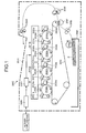
- FIG. 1 is an explanatory diagram of an image forming apparatus according to one embodiment of the present invention.
- the image forming apparatus is a "tandem color printer”.
- a color printer denoted by reference sign 2000 is a multi-color printer that forms a full color image by superimposing four color images (black, cyan, magenta, and yellow).
- the color printer 2000 includes two optical scanning apparatuses 2010a and 2010b.
- the color printer 2000 also includes photosensitive drums 2030a, 2030b, 2030c, and 2030d as four photoreceptors.
- a cleaning unit 2031a, a charging device 2032a, a developing roller 2033a, and a toner cartridge 2034a are arranged around the photosensitive drum 2030a.
- the photosensitive drum 2030a, the cleaning unit 2031a, the charging device 2032a, the developing roller 2033a, and the toner cartridge 2034a form a "station K".
- the "station K” is an image forming station that forms a black image.
- a cleaning unit 2031b, a charging device 2032b, a developing roller 2033b, and a toner cartridge 2034b are arranged around the photosensitive drum 2030b.
- the photosensitive drum 2030b, the cleaning unit 2031b, the charging device 2032b, the developing roller 2033b, and the toner cartridge 2034b form a "station C".
- the "station C” is an image forming station that forms a cyan image.
- a cleaning unit 2031c, a charging device 2032c, a developing roller 2033c, and a toner cartridge 2034c are arranged around the photosensitive drum 2030c.
- the photosensitive drum 2030c, the cleaning unit 2031c, the charging device 2032c, the developing roller 2033c, and the toner cartridge 2034c form a "station M".
- the "station M” is an image forming station that forms a magenta image.
- a cleaning unit 2031d, a charging device 2032d, a developing roller 2033d, and a toner cartridge 2034d are arranged around the photosensitive drum 2030d.
- the photosensitive drum 2030d, the cleaning unit 2031d, the charging device 2032d, the developing roller 2033d, and the toner cartridge 2034d form a "station Y".
- the "station Y" is an image forming station that forms a yellow image.
- a transfer belt 2040, a transfer roller pair 2042, and a fixing device 2050 are arranged below these stations K to Y.
- a paper feed tray 2060, a paper feed roller 2054, and a timing roller pair 2056 are provided below these stations K to Y.
- a paper delivery roller pair 2058 and a paper delivery tray 2070 are arranged in an upper part of the image forming apparatus body.
- a communication control device 2080, a printer control device 2090 that executes the overall control of the respective units, and the like are arranged in the upper part of the image forming apparatus body.
- the communication control device 2080 controls bidirectional communication with a "higher-level device (for example, a computer)" via a network.
- a "higher-level device for example, a computer
- the printer control device 2090 includes a CPU, a ROM, a RAM, an AD converter circuit, and the like.
- a program described in a code readable by the CPU, and various data to be used at the time of executing the program are stored in the ROM.
- the RAM is a work memory, and the AD converter circuit converts analog data to digital data.
- the printer control device 2090 transmits image information from the "higher-level device" to the optical scanning apparatuses 2010a and 2010b.
- the printer control device 2090 also executes various controls of optical scanning performed by the optical scanning apparatuses 2010a and 2010b.
- Circumferential surfaces of the respective photosensitive drums 2030a to 2030d are respectively formed as a photoconductive photosensitive layer.
- Surfaces of the photosensitive layer of the photosensitive drums 2030a to 2030d are "scanning target surfaces" subjected to optical scanning.
- the photosensitive drums 2030a to 2030d are respectively rotated clockwise by a drive unit (not shown).
- the respective photosensitive drums 2030a to 2030d are uniformly charged by the corresponding charging device 2032a to 2032d.
- a corona discharge charging device is exemplified.
- the charging device is not limited thereto, and a contact/non-contact charging device such as a charging roller can be used.
- Optical scanning is performed to the respective uniformly charged photosensitive drums by the optical scanning apparatus.
- the photosensitive drums 2030a and 2030b are optically scanned by the optical scanning apparatus 2010a
- the photosensitive drums 2030c and 2030d are optically scanned by the optical scanning apparatus 2010b.
- Optical scanning is performed "between the charging device and the developing roller".
- the optical scanning apparatus 2010a performs optical scanning based on the respective pieces of image information of black and cyan supplied from the higher-level device via the printer control device 2090.
- the photosensitive drums 2030a and 2030b are optically scanned by the optical scanning.
- a "K latent image" corresponding to the black image information is formed on the photosensitive drum 2030a by the optical scanning.
- a "C latent image” corresponding to the cyan image information is formed on the photosensitive drum 2030b.
- the optical scanning apparatus 2010b performs optical scanning based on magenta image information and yellow image information supplied from the higher-level device via the printer control device 2090.
- the photosensitive drums 2030c and 2030d are optically scanned by the optical scanning.
- an "M latent image” corresponding to the magenta image information is formed on the photosensitive drum 2030c, and a “Y latent image” corresponding to the yellow image information is formed on the photosensitive drum 2030d.
- the K to Y latent images formed on the corresponding photosensitive drums 2030a to 2030d are developed by the corresponding developing roller 2033a to 2033d, respectively.
- the toner cartridge 2034a supplies black toner stored therein to the developing roller 2033a.
- the developing roller 2033a visualizes the K latent image formed on the photosensitive drum 2030a by the supplied black toner.
- the toner cartridge 2034b supplies cyan toner stored therein to the developing roller 2033b.
- the developing roller 2033b visualizes the C latent image formed on the photosensitive drum 2030b by the supplied cyan toner.
- the toner cartridge 2034c supplies magenta toner stored therein to the developing roller 2033c.
- the developing roller 2033c visualizes the M latent image formed on the photosensitive drum 2030c by the supplied magenta toner.
- the toner cartridge 2034d supplies yellow toner stored therein to the developing roller 2033d.
- the developing roller 2033d visualizes the Y latent image formed on the photosensitive drum 2030d by the supplied yellow toner.
- a black image, a cyan image, a magenta image, and a yellow image are formed on the photosensitive drums 2030a to 2030d, respectively.
- toner images are formed by an electrophotographic process on the photosensitive drums 2030a to 2030d, which are a plurality of photoconductive photoreceptors, respectively.
- the color images of black, cyan, magenta, and yellow formed as described above are sequentially transferred onto the transfer belt 2040 at a predetermined timing.
- Transfer of the respective color images onto the transfer belt 2040 can be performed by a known appropriate transfer unit, and the transfer unit is not shown in FIG. 1 .
- the respective color images to be transferred are superimposed on each other on the transfer belt 2040 to form a "color image”.
- Transfer of the respective color images from the respective photosensitive drums onto the transfer belt 2040 is referred to as "primary transfer".
- the color image is transferred to and fixed on a recording sheet, which is a sheet-like recording medium.
- a recording sheet S onto which the color image is transferred and fixed is stacked and stored in the paper feed tray 2060, and is delivered and fed one by one by the paper feed roller 2054.
- a front end of the fed recording sheet S is nipped between the timing roller pair 2056.
- the timing roller pair 2056 delivers the nipped recording sheet S toward a "secondary transfer portion", which is a portion at which the transfer belt 2040 and the transfer roller pair 2042 face each other, at a predetermined timing.
- the color image on the transfer belt 2040 is secondarily transferred to the recording sheet S, when the recording sheet S passes through the secondary transfer portion.
- the color image transferred to the recording sheet S is fixed thereon by the effects of heat and pressure by the fixing device 2050, and the recording sheet S is delivered onto the paper delivery tray 2070 by the paper delivery roller pair 2058.
- the respective cleaning units 2031a to 2031d remove "transfer residual toner" remaining on the surfaces of the corresponding photosensitive drums 2030a to 2030d.
- optical scanning apparatuses 2010a and 2010b are explained next. Because the optical scanning apparatuses 2010a and 2010b have the same configuration, the optical scanning apparatus 2010a is explained below as an example.
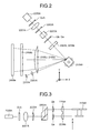
- optical scanning apparatus 2010a An example of the optical scanning apparatus 2010a is explained with reference to FIGS. 2 to 4 .
- reference sign 2200A denotes a "single semiconductor light-emitting element" as a light source
- reference signs QvA, Qa, and Qb denote a "quarter-wave plate” respectively
- reference sign 2201A denotes a "coupling lens”.
- Reference sign 2202A denotes an "aperture plate”
- reference sign 2203A denotes a "light-flux dividing member", which is a light-flux dividing unit
- reference signs 2204a and 2204b denote a "cylindrical lens” respectively.
- Reference sign 2104A denotes a "polygon mirror”.
- Reference signs 2105a and 2105b denote “first scanning lenses”, and reference signs 2107a and 2107b denote “second scanning lenses”.
- Reference signs 2106a, 2106b, 2108a, and 2108b respectively denote an "optical-path bending mirror”.
- a Z direction is a sub-scanning direction
- a Y direction is a main scanning direction.
- the "main scanning direction” is a direction in which the optical scanning apparatuses 2010a and 2010b optically scan the corresponding photosensitive drums (scanning target surfaces).
- the "sub-scanning direction" is a direction orthogonal to the main scanning direction on the scanning target surface.
- main scanning direction directions corresponding to the main scanning direction and the sub-scanning direction are referred to as "main scanning direction” and “sub-scanning direction”, respectively, even on an optical axis and an optical path of the light flux extending from the semiconductor light-emitting element 2200A to each of the scanning target surfaces.
- the semiconductor light-emitting element 2200A is a "semiconductor laser", and emits a linearly polarized light flux (a single light flux) having a predetermined wavelength (in this example, a 780-nm band).
- the emitted light flux enters into the quarter-wave plate QvA, and is provided with an "optical phase difference of a quarter-wavelength" and converted to circularly polarized light.
- the quarter-wave plate QvA is inclined with respect to a surface orthogonal to a traveling direction of the light flux, and a light flux reflected by the quarter-wave plate QvA decreases an "amount returning to the semiconductor light-emitting element 2200A".
- the light flux having passed through the quarter-wave plate QvA is changed to a substantially parallel light flux by the coupling lens 2201A, and is so-called beam-shaped by an opening of the aperture plate 2202A.
- the light-flux dividing member 2203A divides the beam-shaped light flux into two light fluxes.
- reference sign L0 denotes a light flux entering from the aperture plate 2202A into the light-flux dividing member 2203A.
- the light flux L0 is "circularly polarized light”.
- the light-flux dividing member 2203A is formed by combining a triangular prism P1 having a sectional shape of right-angled triangle and a square prism P2 having a sectional shape of parallelogram.
- a bonded surface of these prisms P1 and P2 forms a "polarization separation surface", which transmits a light flux L1 having a P polarization component of the light flux L0 incident thereto, and reflects a light flux L2 having an S polarization component.
- the light flux L2 reflected by the polarization separation surface is reflected by a "reflecting mirror surface" on an upper surface of the square prism P2, "is separated in parallel” from the light flux L1, and is emitted from the light-flux dividing member 2203A.
- the light flux L0 from the semiconductor light-emitting element 2200A is divided into two light fluxes L1 and L2 parallel to each other in the sub-scanning direction by the light-flux dividing member 2203A.
- the light flux emitted from the semiconductor light-emitting element 2200A as the light source is spatially divided into plural (two) by the light-flux dividing member 2203A, which is the light-flux dividing unit.
- the division number of the light flux by the light-flux dividing member 2203A is two.
- the light flux is divided by the light-flux dividing member 2203A by using the polarization property.
- a first light flux (the light flux L1), which is one of the two light fluxes emitted from the light-flux dividing member 2203A, enters into the quarter-wave plate Qa and is converted to the circularly polarized light.
- a second light flux (the light flux L2), which is the other of the two light fluxes emitted from the light-flux dividing member 2203A, enters into the quarter-wave plate Qb and is converted to the circularly polarized light.
- the light fluxes converted to the circularly polarized light in this manner enter into the cylindrical lens 2204a, 2204b, respectively and are focused in the sub-scanning direction (the Z direction in FIG. 3 ).
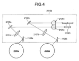
- a four-fold mirror having four deflective reflection surfaces is "arranged in two stages in the sub-scanning direction".
- the light flux (the light flux L2) from the cylindrical lens 2204b enters into the deflective reflection surface and is deflected.
- the light flux (the light flux L1) from the cylindrical lens 2204a is deflected.
- the respective light fluxes L1 and L2 are imaged as a "line image long in the main scanning direction" near the deflective reflection surface of the four-fold mirror, to which the light fluxes enter, by the operations of the cylindrical lenses 2204a and 2204b.
- the four-fold mirrors on the first stage and the second stage respectively "rotate with a phase being shifted by 45 degrees".
- the two first scanning lenses 2105a and 2105b shown in FIGS. 2 and 4 respectively have an "f ⁇ function".
- the first scanning lenses 2105a and 2105b have a function of equalizing the main scanning speed on the corresponding photosensitive drum surface by the light flux deflected at an equiangular speed with rotation of the polygon mirror 2104A.
- the first scanning lenses 2105a and 2105b are overlapped in the Z direction (the sub-scanning direction).
- the first scanning lens 2105a faces the "lower four-fold mirror", and the first scanning lens 2105b faces the "upper four-fold mirror”.
- the light flux deflected by the "upper four-fold mirror” of the polygon mirror 2104A is transmitted through the first scanning lens 2105b, and the optical path thereof is bent by the optical-path bending mirror 2106b.
- the light flux is then emitted to the photosensitive drum 2030b via the second scanning lens 2107b and the optical-path bending mirror 2108b to form an optical spot.
- the optical spot scans the photosensitive drum 2030b in the main scanning direction at the constant speed with the rotation of the polygon mirror 2104A, thereby writing a cyan image.
- the light flux deflected by the "lower four-fold mirror” of the polygon mirror 2104A is transmitted through the first scanning lens 2105a, and the optical path thereof is bent by the optical-path bending mirror 2106a.
- the light flux is then emitted to the photosensitive drum 2030a via the second scanning lens 2107a and the optical-path bending mirror 2108a to form an optical spot.
- the optical spot scans the photosensitive drum 2030a in the main scanning direction at the constant speed with the rotation of the polygon mirror 2104A, thereby writing a black image.
- the respective optical-path bending mirrors are provided so that the respective optical path lengths from the polygon mirror 2104A to the respective photosensitive drums match with each other.
- the respective optical-path bending mirrors are also provided so that respective "incident positions and incident angles of the light flux to the photosensitive drum" are equivalent to each other.
- the cylindrical lenses 2204a and 2204b and the second scanning lenses 2107a and 2107b corresponding thereto form a so-called "optical face tangle error correction system".
- the "line image" described above formed by the cylindrical lens 2204a and the scanning direction of the photosensitive drum 2030a have a conjugate relation by the second scanning lens 2107a in the sub-scanning direction.
- the "line image" described above formed by the cylindrical lens 2204b and the scanning direction of the photosensitive drum 2030b have also a conjugate relation by the second scanning lens 2107b in the sub-scanning direction.
- the first scanning lenses 2105a and 2105b, the second scanning lenses 2107a and 2107b, and the optical-path bending mirrors 2106a, 2106b, 2108a, and 2108b form a scanning optical system.
- the configuration described above is a configuration of the optical scanning apparatus 2010a that optically scans the photosensitive drums 2030a and 2030b.
- the first scanning lens 2105a, the second scanning lens 2107a, and the optical-path bending mirrors 2106a and 2108a form a "scanning optical system of the station K".
- first scanning lens 2105b, the second scanning lens 2107b, and the optical-path bending mirrors 2106b and 2108b form a "scanning optical system of the station C".
- the optical scanning apparatus 2010b that optically scans the photosensitive drums 2030c and 2030d have the same configuration as that of the optical scanning apparatus 2010a.
- an optical scanning area in the main scanning direction of each photosensitive drum in which image information is written is referred to as "effective scanning area”.
- reference sign 2301A denotes a "synchronization lens”
- reference sign 2302A denotes a "synchronization detection sensor”.
- the synchronization lens 2301A is used for detecting a deflected light flux (the light flux L1) deflected by the "lower-stage four-fold mirror" of the polygon mirror 2104A.
- the synchronization lens 2301A is arranged on an optical path of the deflected light flux transmitted through a "non-power portion having no power in the main scanning direction" at an end on a -Y side of the first scanning lens 2105b.
- the deflected light flux is focused onto a light-receiving surface of the synchronization detection sensor 2302A.
- the synchronization detection sensor 2302A outputs a signal corresponding to an amount of light of the light-received deflected light flux to the printer control device 2090 that controls optical scanning.
- the printer control device 2090 determines a "write start timing with respect to the photosensitive drums 2030a and 2030b, based on the signal output from the synchronization detection sensor 2302A.
- the synchronization lens 2301A and the synchronization detection sensor 2302A constitute a "synchronization detection system”.
- the deflected light flux light-received by the synchronization detection sensor 2302A is referred to as "light flux for synchronization detection”.
- the light flux for synchronization detection passes through the non-power portion of the first scanning lens 2105a, and the optical path of the light flux for synchronization detection does not change regardless of deformation of the first scanning lens due to a change in the ambient temperature.
- the two light fluxes L1 and L2 from the semiconductor light-emitting element 2200A scan one of the photosensitive drums, the two light fluxes L1 and L2 do not reach the other photosensitive drum.
- a "light-source drive unit” (not shown) modulates and drives the semiconductor light-emitting element 2200A based on the black image information.
- the light-source drive unit modulates and drives the semiconductor light-emitting element 2200A based on the cyan image information.
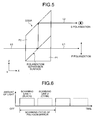
- FIG. 6 A time chart for optical scanning with respect to the photosensitive drums 2030a and 2030b in this case is shown in FIG. 6 .
- an "amount of light" of exposure is plotted on a vertical axis and "time” is plotted on a horizontal axis.
- Exposure by the black image information and the cyan image information is performed by the light flux from the semiconductor light-emitting element 2200A as a common light source.
- each of the spatially separated light fluxes L1 and L2 is "spatially separated” and deflected alternately by the polygon mirror 2104A as the optical deflector.
- Scanning of the different photoreceptor is performed by each of the deflected light fluxes.
- the time chart shows a timing when the light is all turned on in the effective scanning areas of the photosensitive drums.
- a solid line corresponds to a portion of the black image information
- a broken line corresponds to a portion of the cyan image information.
- scanning line 1 means a scanning line by the light flux L1 (a trajectory of the optical spot that performs main scanning)
- scanning line 2 means a scanning line by the light flux L2.
- optical scanning of the respective photosensitive drums 2030a to 2030d is performed as described above by the optical scanning apparatuses 2010a and 2010b.
- the image forming apparatus in FIG. 1 can perform "image formation using only a part" of the four image forming stations.
- image formation is not performed by at least one of the four image forming stations.
- Modulation drive of the semiconductor light-emitting element 2200A that is required for forming a black image is performed after a determination of the write start timing of the black image and the cyan image by the synchronization detection system.
- the semiconductor light-emitting element 2200A is forcibly lighted up and deflected, and the light flux for synchronization detection is received by the synchronization detection sensor 2302A.
- optical scanning is performed not only on the synchronization detection sensor 2302A but also on the photosensitive drums 2030a and 2030b.
- offset light emission is performed by the semiconductor light-emitting element for improving rise characteristics and power stability of optical power of the semiconductor light-emitting element 2200A.
- offset beams Due to the offset light emission, “offset beams” are always emitted, although in a limited amount of light.
- the photosensitive drum 2030b for forming a cyan image is exposed to the offset beams.
- the exposure of the photosensitive drum 2030b to the offset beams causes deterioration of the photosensitive drum 2030b due to light-induced fatigue.
- the at least one optical-path opening/closing unit is arranged in at least one optical path of the light fluxes divided by the light-flux dividing unit to open or close the optical path independently.
- the control unit controls opening/closing of the optical path by the at least one optical-path opening/closing unit.
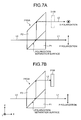
- FIGS. 7A and 7B depict one embodiment of the optical-path opening/closing unit.
- a shielding member 2109 (and a drive unit (not shown)) are provided as the optical-path opening/closing unit between the light-flux dividing member 2203A and the scanning target surface.
- the shielding member 2109 is provided to open or close the optical path of one of the divided light fluxes (the light flux L2 that performs write of a cyan image).
- the shielding member 2109 shields the light flux L2 guided in the optical path that is opened or closed.
- the position where the shielding member 2109 is installed can be basically any position from a position after the light flux from the semiconductor light-emitting element is divided into two by the light-flux dividing unit up to a position of the photosensitive drum surface.
- a position before the light flux is deflected by the optical deflector is advantageous in view of the installation space and cost, because the size of the shielding member 2109 can be decreased.
- the shielding member 2109 is arranged on an optical path of the light flux L2 at a position immediately after the light-flux dividing member 2203A.
- the shielding member 2109 is driven to move parallel to a Y direction orthogonal to the drawing by a drive unit (not shown, being controlled by the printer control device 2090 in FIG. 1 ).
- the shielding member 2109 and the drive unit form the "optical-path opening/closing unit"
- the printer control device 2090 forms the "control unit”.
- the shielding member 2109 can switch the "opened or closed state of the optical path" depending on the input image information.
- FIG. 7A This state is shown in FIG. 7A .
- the shielding member 2109 is retreated from the optical path of the light flux L2, as shown by a broken line, and does not close any optical path.
- the input image information is used to form a monochrome image (forming a black image)
- only one of the divided light fluxes (the light flux L1) is required, and the other (the light flux L2) is not required.
- the shielding member 2109 is displaced in the Y direction by the drive unit (not shown), so that only the optical path of the light flux L2 is shielded. This state is shown in FIG. 7B .
- the optical path of the light flux L2 is closed by the shielding member 2109. Therefore, the photosensitive drum 2030b is not optically scanned by the light flux L2 (offset beams).
- the shielding member 2109 moves into and out from the optical path of the light flux L2 with simple parallel displacement to open or close the optical path.
- the drive unit that displaces and drives the shielding member 2109 causes the shielding member 2109 to perform simple reciprocating parallel displacement.
- a "known appropriate parallel displacement mechanism” can be used, and opening/closing control of the optical path can be executed according to the image to be formed.
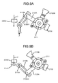
- FIGS. 8A and 8B Another embodiment of the present invention is explained with reference to FIGS. 8A and 8B .
- a shielding unit as the optical-path opening/closing unit is provided between the light-flux dividing member 2203A and the scanning target surface.
- the shielding unit is provided to open or close the optical path of one of the divided light fluxes (the light flux L2 that performs write of a cyan image).
- the shielding unit includes a swingable shielding member 2110 and a drive unit 2111 that drives the shielding member 2110.
- the drive unit 2111 is a "stepping motor”.
- FIG. 8A depicts a state where the optical paths of both the light fluxes L1 and L2 are opened.
- FIG. 8B depicts a state where the optical path of the light flux L2 is closed.
- the light fluxes L1 and L2 are overlapped on each other in the sub-scanning direction orthogonal to the drawing.
- the shielding member 2110 is rotated counterclockwise 90 degrees from the state in FIG. 8A by the stepping motor 2111 and is arranged in the optical path of the light flux L2.
- the optical path of the light flux L2 is closed by the arrangement of the shielding member 2110.
- the shielding member 2110 When the shielding member 2110 is rotated clockwise 90 degrees from the state in FIG. 8B , the shielding member 2110 is retreated from the optical path of the light flux L2 to open the optical path of the light flux L2.
- the working speed of the shielding member 2110 can be such that an opening/closing operation is complete within a time (within several hundreds of milliseconds) from an input of the image information until synchronization detection light is emitted.
- the stepping motor 2111 as the drive unit only needs to be operated while being matched with the time.
- the stepping motor 2111 can rotate at a certain angle according to an input signal, and can perform the opening/closing operation without executing any complicated control.
- an optical sensor 2112b and an actuator 2112a are provided.
- the actuator 2112a is integrally provided with the shielding member 2110.
- the actuator 2112a puts the optical sensor 2112b in a shielded state.
- the actuator 2112a puts the optical sensor 2112b in an opened state, and the optical sensor 2112b is turned ON.
- FIGS. 9A and 9B Three examples of other embodiments are explained with reference to FIGS. 9A and 9B .
- reference signs 2203A, 2110, and 2111 respectively denote the light-flux dividing member, the shielding member, and the stepping motor as in FIGS. 8A and 8B .
- the shielding member 2110 can rotate in forward and reverse directions, and rotates around a rotation shaft 2110A in the forward and reverse directions to open and close the optical path of the light flux L2.
- FIG. 9A depicts an opened state
- FIG. 9B depicts a shielded state.
- a rotary drive unit 2110B is integrally formed with the shielding member 2110.
- the rotary drive unit 2110B is in a "U shape" in this example, and has a gap parallel to a longitudinal direction thereof.
- a pin 2120A1 fixed and provided near the end of an arm 2120A of the drive member is inserted into the gap with a backlash.
- the drive member includes another arm 2120B integrally formed with the arm 2120A.
- the drive member is rotated in the forward and reverse directions around a shaft orthogonal to the drawing of FIGS. 9A and 9B by the stepping motor 2111 as the drive unit.
- a rotation shaft of the drive member is coaxial with a drive shaft of the stepping motor 2111.
- the arm 2120A of the drive member, the rotary drive unit 2110B, and the pin 2120A1 constitute a link mechanism.
- the drive member is rotated counterclockwise a predetermined angle by the stepping motor 2111, from a state shown in FIG. 9A where the optical path of the light flux L2 is opened.
- the rotary drive unit 2110B is then rotated clockwise, and as shown in FIG. 9B , the shielding member 2110 closes the optical path of the light flux L2.
- the optical path of the light flux L1 explained with reference to FIGS. 8A and 8B is not opened or closed as in the embodiment shown in FIGS. 8A and 8B .
- a part denoted by reference sign 2130 is a signal input unit to the stepping motor 2111.
- the shielding member 2110 rotates counterclockwise substantially 90 degrees from the state in FIG. 9B to open the optical path.
- the working speed of the shielding member 2110 can be such that the opening/closing operation is complete within a time (within several hundreds of milliseconds) from an input of the image information until synchronization detection light is emitted.
- the stepping motor 2111 as the drive unit only needs to be operated while being matched with the time.
- the operation control is also executed by the printer control device 2090 in FIG. 1 .
- the stepping motor 2111 can rotate at a certain angle according to an input signal, and can perform the opening/closing operation without executing any complicated control.
- the optical-path opening/closing unit constitutes the "link mechanism" as described above, and a displacement amount of the arm 2120A of the drive member and the shielding member 2110 can be set differently from each other.
- design flexibility and layout flexibility with respect to the optical-path opening/closing unit can be considerably improved by the drive unit, as compared to a case where the shielding member is directly operated.
- the optical-path opening/closing unit can be installed at a "position having little room for layout" such as in a pre-deflection optical system.
- FIGS. 9A and 9B realizes this state.
- the longitudinal direction of the gap in the rotary drive unit 2110B is approximately parallel to a "shift direction of the pin 2120A1 due to the rotation of the drive member".
- a rotation angle of the shielding member 2110 is smaller than that of the drive member.
- the rotation angle of the shielding member 2110 is smaller than that of the drive member.
- an amount of displacement of the shielding member 2110 by the drive member of the optical path opening/closing member at the time of fully opening/closing the optical path is smaller than that at the time of halfway opening/closing the optical path.
- the "fully opening/closing the optical path” means that opening/closing of the optical path is completely performed.
- the "halfway opening/closing the optical path" means that opening/closing of the optical path is incomplete.
- FIG. 10 is an explanatory diagram of another embodiment of the present invention.
- a planar shape of the drive member is not axisymmetric to the rotation shaft of the stepping motor 2111.
- a center of gravity of the drive member is away from the rotation shaft of the stepping motor 2111.
- a centrifugal force acting on the drive member at the time of rotation of the drive member also increases with an increase of the distance "d", and counteraction thereof acts on the rotation shaft of the stepping motor 2111.
- FIG. 10 The embodiment shown in FIG. 10 is an exemplary embodiment considering this point.
- FIG. 10 depicts a state as viewed from below the stepping motor 2111. To avoid complexity, like reference signs to those of FIGS. 9A and 9B are added to like parts in FIG. 10 , for which any confusion is unlikely to occur.
- reference sign 2120 denotes a "drive member”.
- the drive member 2120 includes arms 2120A and 2120D.
- the arm 2120D has a different shape from that of the arm 2120B shown in FIGS. 9A and 9B .
- the drive member 2120 has a "structural portion" denoted by reference sign 2120C.
- the structural portion 2120C includes a "half-cut hollow cylindrical portion” and a radial "half-cut wheel shaft portion”, and is integrally formed with the drive member 2120.
- the structural portion 2120C is a "counter-balanced portion" with respect to the arms 2120A and 2120D.
- the center of gravity of the drive member 2120 can be set near the rotation shaft of the stepping motor 2111, thereby enabling to decrease the distance "d".
- rotation of the drive member 2120 can be stabilized and the opening/closing operation of the shielding member 2110 can be also stabilized.
- FIGS. 11A and 11B is an example in which a detecting unit 2140 that detects the opened/closed state of the optical path by the optical-path opening/closing unit is provided with respect to the embodiment explained with reference to FIGS. 9A and 9B .
- the end of the arm 2120B is bent substantially parallel to the drive shaft of the stepping motor 2111.
- the bent portion is a shielding portion 2120B1 with respect to an optical sensor 2140.
- the shielding portion 2120B1 shields "between a light emitting part and a light receiving part" of a sensor unit 2140A of the optical sensor 2140 shown in FIG. 11B .
- the shielding portion 2120B1 is positioned between the light emitting part and the light receiving part of the sensor unit 2140A.
- This state is a "Hi" state of the optical sensor 2140.
- the shielding portion 2120B1 is retreated from between the light emitting part and the light receiving part of the sensor unit 2140A, and the optical sensor 2140 is in a "Lo" state.
- the "Hi” and “Lo” of the optical sensor 2140 are switched in this manner while being associated with the rotation of the drive member by the stepping motor 2111.
- the opened/closed state of the optical path of the light flux L2 can be reliably detected.
- the "member emitted with the light flux" of the shielding member 2110 can be formed in a black piled form to increase optical absorptance, and reflection and scattering of the shielded light flux can be suppressed.
- the shielding portion can be integrally formed with the shielding member 2110 instead of being provided in the drive member as shown in FIGS. 11 , so that rotation of the shielding member 2110 can be directly detected.
- the opened/closed state of the optical path can be detected more reliably.
- the structural portion 2120C is formed as a "counter balance" in the drive member.
- the structural portion 2120C can be formed in the drive member in the embodiments shown in FIGS. 9 and 11 .
- the image forming apparatus shown in FIG. 1 has four photoreceptors, and forms a four-color toner image thereon that is required for forming a color image.
- optical scanning apparatuses 2010a and 2010b used in the image forming apparatus.
- the present invention is not limited thereto, and any one of the optical scanning apparatuses 2010a and 2010b can be used to carry out an image forming apparatus that forms a two-color image such as red and black.
- the light source is not limited thereto, and a light source "that includes a plurality of light emitting parts and can emit a plurality of light fluxes independently" can be also used.
- the light source is not limited to the one described above, and can be an edge-emitting semiconductor laser array or a surface-emitting semiconductor laser (VCSEL).
- VCSEL surface-emitting semiconductor laser
- a "light flux emitted from a light source” claimed in claim 1 means an "aggregate of light fluxes" to be emitted.
- the light-flux dividing unit divides the light flux into a plurality of light fluxes, in a unit of "aggregate of light fluxes", and the divided “one unit of light flux” includes a plurality of light fluxes.
- the divided one unit of light flux is focused as "two or more optical spots" on the surface to be optically scanned. "Multi-beam scanning” is performed by these plural spots.
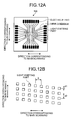
- FIGS. 12A and 12B are explanatory diagrams of a "VCSEL" as an example of the semiconductor light-emitting element that emits the light fluxes independently.
- a VCSEL 100 includes "32 light emitting parts" two-dimensionally arranged on the same substrate, and electrode pads and wiring members arranged and connected to surround these light emitting parts.
- FIG. 12B depicts an arranged state of the light emitting parts.
- the 32 light emitting parts are arranged such that adjacent light emitting parts are arranged in the main scanning direction (a direction corresponding to the main scanning in FIG. 12A ) with a gap: X.
- the light emitting parts are arranged such that adjacent light emitting parts are arranged in the sub-scanning direction (a direction corresponding to the sub-scanning in FIG. 12B ) with a gap: d2.
- the adjacent light emitting parts are “displaced” by a distance: d1 in the sub-scanning direction.
- This displacement is set so that a projected gap of the light emitting parts becomes an equal gap: d1, when all the light emitting parts are "orthographically projected on a virtual line extending in the sub-scanning direction".
- an optical path to a scanning target surface, which does not need to be optically scanned, among a plurality of scanning target surfaces can be closed.
Landscapes
- Engineering & Computer Science (AREA)
- Multimedia (AREA)
- Signal Processing (AREA)
- Physics & Mathematics (AREA)
- General Physics & Mathematics (AREA)
- Facsimile Scanning Arrangements (AREA)
- Mechanical Optical Scanning Systems (AREA)
- Laser Beam Printer (AREA)
Abstract
Description
- The present application claims priority to and incorporates by reference the entire contents of Japanese Patent Application No.
2012-257389 2013-035063 - The present invention relates to an optical scanning apparatus, a method for performing the same and an image forming apparatus.
- The image forming apparatus according to the present invention performs image formation by an electrophotographic process.
- That is, the image forming apparatus according to the present invention can be carried out as an optical printer such as a laser printer, an optical plotter, a digital electronic copier, a plain paper facsimile, and the like.
- Recently, for an image forming apparatus such as a laser printer, a digital electronic copier, and a plain paper facsimile, colorization of formed images, an increase in the speed, and downsizing of the apparatus have been demanded.
- In response to such demands, various image forming apparatuses that use a plurality of photoconductive photoreceptors have been proposed and realized.
- As such an image forming apparatus, an apparatus that "shares a light source for optical scanning" with respect to a plurality of photoreceptors has been proposed (Japanese Patent Application Laid-open No.
2012-145667 - As a light source for optical scanning in an image forming apparatus, a "semiconductor light-emitting element" such as a semiconductor laser or a surface-emitting semiconductor laser (so-called "vertical-cavity surface-emitting later (VCSEL)") is generally used.
- High-speed drive of these "semiconductor light-emitting elements" has been realized and a signal for modulating exposure energy based on image information becomes a "modulation signal of a higher frequency" from several to several tens of megahertz.
- In a semiconductor light-emitting element used for such a "modulation signal of an extremely high frequency", "offset light emission" is always performed for light-emission rise characteristics and stability of light-emitting power.
- The offset light emission means to emit light with constant weak light emission intensity during optical scanning, even during a time when light emission does not contribute to image write based on image information.
- When a semiconductor light-emitting element as a light source is shared by a plurality of photoreceptors and the "offset light emission" is performed by using the shared semiconductor light-emitting element, there are following problems.
- For specific explanation, there is assumed a case where "one semiconductor light-emitting element is shared by two photoreceptors", and an image A is formed on one of the photoreceptors and an image B is formed on the other.
- The images A and B are, for example, a cyan image and a black image used for forming a color image.
- In this case, when both the images A and B are formed, light emission from the semiconductor light-emitting element is continuously performed, and modulation is performed alternately by a modulation signal for writing the image A and a modulation signal for writing the image B.
- When only the image A is formed, the photoreceptor for the image A is optically scanned by "modulated light"; however, the photoreceptor for the image B is optically scanned by "offset light emission".
- In this case, when the photoreceptor for the image B is stopped to save energy for driving the photoreceptor, the same spot of the photoreceptor is "optically scanned repeatedly by the offset light emission".
- Therefore, light-induced fatigue occurs in a "portion which is optically scanned repeatedly" of the photoreceptor, and the photosensitive property thereof tends to be deteriorated. Such deterioration of the photosensitive property occurs "in a line shape".
- When the image B is formed by using the "photoreceptor in which the photosensitive property is deteriorated in the line shape", an abnormal image is formed such that streaky density unevenness appears due to the deterioration of the photosensitive property in the line shape.
- Therefore, there is a need to provide an optical scanning apparatus that favorably prevents the abnormal image described above.
- It is an aim of the present invention to at least partially solve the problems in the conventional technology.
- According to an aspect of the invention, an optical scanning apparatus for optically scanning at least one scanning target surface is provided. The optical scanning apparatus includes: a light source; a light-flux dividing unit disposed on a main optical path of a main light flux emitted from the light source, and the light-flux dividing unit configured to spatially divide the main light flux;
an optical deflector disposed on a divided optical path of the divided light flux, and the optical deflector configured to deflect the divided optical path; an optical path opening/closing switch unit disposed on the divided optical path between the light-flux dividing unit and the optical deflector, and the optical path opening/closing switch unit configured to interrupt or pass at least one of the divided optical path; and a controller configured to control operation of interrupting or passing the at least one of the divided optical path by the optical path opening/closing switch unit. - According to another aspect of the invention, an image forming apparatus is provided. The image forming apparatus includes: at least one photoreceptor; an optical scanning apparatus set forth in
claim 1 for writing an electrostatic image onto the at least one photoreceptor; and a transferring unit configured to superimpose different color of toner images and transferring the superimposed image onto a common sheet-like recording medium, and fixing the transferred image thereon. - According to further aspect of the invention, a method for performing an optical scanning apparatus for optically scanning at least one scanning target surface is provided. The optical scanning apparatus includes: a light source; a light-flux dividing unit disposed on a main optical path of a main light flux emitted from the light source, and the light-flux dividing unit configured to spatially divide the main light flux; an optical deflector disposed on a divided optical path of the divided light flux, and the optical deflector configured to deflect the divided optical path; an optical path opening/closing switch unit disposed on the divided optical path between the light-flux dividing unit and the optical deflector, and the optical path opening/closing switch unit configured to interrupt or pass at least one of the divided optical path; and a controller configured to control operation of interrupting or passing the at least one of the divided optical path by the optical path opening/closing switch unit. The method includes: emitting the main light flux from the light source; dividing spatially the main light flux; interrupting the at least one of the divided optical path; and deflecting the divided optical path passing the optical path opening/closing switch unit.
- The above and other aims, features, advantages and technical and industrial significance of this invention will be better understood by reading the following detailed description of presently preferred embodiments of the invention, when considered in connection with the accompanying drawings, in which:
-
FIG. 1 is an explanatory diagram of an image forming apparatus according to one embodiment of the present invention; -
FIG. 2 is an explanatory diagram of an optical scanning apparatus; -
FIG. 3 is another explanatory diagram of the optical scanning apparatus; -
FIG. 4 is still another explanatory diagram of the optical scanning apparatus; -
FIG. 5 is an explanatory diagram of division of a light flux; -
FIG. 6 is an explanatory diagram of optically scanning two scanning target surfaces with light fluxes from one light source; -
FIGS. 7A and 7B are explanatory diagrams of an example of optical path opening/closing by an optical-path opening/closing unit; -
FIGS. 8A and 8B are explanatory diagrams of another example of the optical path opening/closing by the optical-path opening/closing unit; -
FIGS. 9A and 9B are explanatory diagrams of another example of the optical path opening/closing by the optical-path opening/closing unit; -
FIG. 10 is an explanatory diagram of still another example of the optical path opening/closing by the optical-path opening/closing unit; -
FIGS. 11A and 11B are explanatory diagram of still another example of the optical path opening/closing by the optical-path opening/closing unit; and -
FIGS. 12A and 12B are explanatory diagram of a VCSEL as an example of a semiconductor light-emitting element. - Exemplary embodiments of the present invention are explained below.
-
FIG. 1 is an explanatory diagram of an image forming apparatus according to one embodiment of the present invention. - The image forming apparatus is a "tandem color printer".
- A color printer denoted by
reference sign 2000 is a multi-color printer that forms a full color image by superimposing four color images (black, cyan, magenta, and yellow). - The
color printer 2000 includes twooptical scanning apparatuses - The
color printer 2000 also includesphotosensitive drums - A
cleaning unit 2031a, acharging device 2032a, a developingroller 2033a, and atoner cartridge 2034a are arranged around thephotosensitive drum 2030a. - The
photosensitive drum 2030a, thecleaning unit 2031a, thecharging device 2032a, the developingroller 2033a, and thetoner cartridge 2034a form a "station K". - The "station K" is an image forming station that forms a black image.
- A
cleaning unit 2031b, acharging device 2032b, a developingroller 2033b, and atoner cartridge 2034b are arranged around thephotosensitive drum 2030b. - The
photosensitive drum 2030b, thecleaning unit 2031b, thecharging device 2032b, the developingroller 2033b, and thetoner cartridge 2034b form a "station C". - The "station C" is an image forming station that forms a cyan image.
- A
cleaning unit 2031c, acharging device 2032c, a developingroller 2033c, and atoner cartridge 2034c are arranged around thephotosensitive drum 2030c. - The
photosensitive drum 2030c, thecleaning unit 2031c, thecharging device 2032c, the developingroller 2033c, and thetoner cartridge 2034c form a "station M". - The "station M" is an image forming station that forms a magenta image.
- A
cleaning unit 2031d, acharging device 2032d, a developingroller 2033d, and atoner cartridge 2034d are arranged around thephotosensitive drum 2030d. - The
photosensitive drum 2030d, thecleaning unit 2031d, thecharging device 2032d, the developingroller 2033d, and thetoner cartridge 2034d form a "station Y". - The "station Y" is an image forming station that forms a yellow image.
- A
transfer belt 2040, atransfer roller pair 2042, and afixing device 2050 are arranged below these stations K to Y. - A
paper feed tray 2060, apaper feed roller 2054, and atiming roller pair 2056 are provided below these stations K to Y. - A paper
delivery roller pair 2058 and apaper delivery tray 2070 are arranged in an upper part of the image forming apparatus body. - A
communication control device 2080, aprinter control device 2090 that executes the overall control of the respective units, and the like are arranged in the upper part of the image forming apparatus body. - The
communication control device 2080 controls bidirectional communication with a "higher-level device (for example, a computer)" via a network. - The
printer control device 2090 includes a CPU, a ROM, a RAM, an AD converter circuit, and the like. - A program described in a code readable by the CPU, and various data to be used at the time of executing the program are stored in the ROM.
- The RAM is a work memory, and the AD converter circuit converts analog data to digital data.
- The
printer control device 2090 transmits image information from the "higher-level device" to theoptical scanning apparatuses - The
printer control device 2090 also executes various controls of optical scanning performed by theoptical scanning apparatuses - Circumferential surfaces of the respective
photosensitive drums 2030a to 2030d are respectively formed as a photoconductive photosensitive layer. - Surfaces of the photosensitive layer of the
photosensitive drums 2030a to 2030d are "scanning target surfaces" subjected to optical scanning. - When the full color image is formed, the
photosensitive drums 2030a to 2030d are respectively rotated clockwise by a drive unit (not shown). - The respective
photosensitive drums 2030a to 2030d are uniformly charged by thecorresponding charging device 2032a to 2032d. - In this exemplary embodiment, a corona discharge charging device is exemplified. However, the charging device is not limited thereto, and a contact/non-contact charging device such as a charging roller can be used.
- Optical scanning is performed to the respective uniformly charged photosensitive drums by the optical scanning apparatus.
- That is, the
photosensitive drums optical scanning apparatus 2010a, and thephotosensitive drums optical scanning apparatus 2010b. - Optical scanning is performed "between the charging device and the developing roller".
- The
optical scanning apparatus 2010a performs optical scanning based on the respective pieces of image information of black and cyan supplied from the higher-level device via theprinter control device 2090. - The
photosensitive drums - A "K latent image" corresponding to the black image information is formed on the
photosensitive drum 2030a by the optical scanning. - A "C latent image" corresponding to the cyan image information is formed on the
photosensitive drum 2030b. - Similarly, the
optical scanning apparatus 2010b performs optical scanning based on magenta image information and yellow image information supplied from the higher-level device via theprinter control device 2090. - The
photosensitive drums - With the optical scanning, an "M latent image" corresponding to the magenta image information is formed on the
photosensitive drum 2030c, and a "Y latent image" corresponding to the yellow image information is formed on thephotosensitive drum 2030d. - The K to Y latent images formed on the corresponding
photosensitive drums 2030a to 2030d are developed by the corresponding developingroller 2033a to 2033d, respectively. - That is, the
toner cartridge 2034a supplies black toner stored therein to the developingroller 2033a. - The developing
roller 2033a visualizes the K latent image formed on thephotosensitive drum 2030a by the supplied black toner. - The
toner cartridge 2034b supplies cyan toner stored therein to the developingroller 2033b. - The developing
roller 2033b visualizes the C latent image formed on thephotosensitive drum 2030b by the supplied cyan toner. - The
toner cartridge 2034c supplies magenta toner stored therein to the developingroller 2033c. - The developing
roller 2033c visualizes the M latent image formed on thephotosensitive drum 2030c by the supplied magenta toner. - The
toner cartridge 2034d supplies yellow toner stored therein to the developingroller 2033d. - The developing
roller 2033d visualizes the Y latent image formed on thephotosensitive drum 2030d by the supplied yellow toner. - In this way, a black image, a cyan image, a magenta image, and a yellow image are formed on the
photosensitive drums 2030a to 2030d, respectively. - That is, different toner images are formed by an electrophotographic process on the
photosensitive drums 2030a to 2030d, which are a plurality of photoconductive photoreceptors, respectively. - The color images of black, cyan, magenta, and yellow formed as described above are sequentially transferred onto the
transfer belt 2040 at a predetermined timing. - Transfer of the respective color images onto the
transfer belt 2040 can be performed by a known appropriate transfer unit, and the transfer unit is not shown inFIG. 1 . - The respective color images to be transferred are superimposed on each other on the
transfer belt 2040 to form a "color image". - Transfer of the respective color images from the respective photosensitive drums onto the
transfer belt 2040 is referred to as "primary transfer". The color image is transferred to and fixed on a recording sheet, which is a sheet-like recording medium. - That is, a recording sheet S onto which the color image is transferred and fixed is stacked and stored in the
paper feed tray 2060, and is delivered and fed one by one by thepaper feed roller 2054. - A front end of the fed recording sheet S is nipped between the
timing roller pair 2056. - The
timing roller pair 2056 delivers the nipped recording sheet S toward a "secondary transfer portion", which is a portion at which thetransfer belt 2040 and thetransfer roller pair 2042 face each other, at a predetermined timing. - The color image on the
transfer belt 2040 is secondarily transferred to the recording sheet S, when the recording sheet S passes through the secondary transfer portion. - The color image transferred to the recording sheet S is fixed thereon by the effects of heat and pressure by the
fixing device 2050, and the recording sheet S is delivered onto thepaper delivery tray 2070 by the paperdelivery roller pair 2058. - The
respective cleaning units 2031a to 2031d remove "transfer residual toner" remaining on the surfaces of the correspondingphotosensitive drums 2030a to 2030d. - The surfaces of the respective photosensitive drums, from which the transfer residual toner has been removed, return to a position facing the corresponding charging device again.
- The
optical scanning apparatuses optical scanning apparatuses optical scanning apparatus 2010a is explained below as an example. - An example of the
optical scanning apparatus 2010a is explained with reference toFIGS. 2 to 4 . - In
FIGS. 2 to 4 ,reference sign 2200A denotes a "single semiconductor light-emitting element" as a light source, reference signs QvA, Qa, and Qb denote a "quarter-wave plate" respectively, andreference sign 2201A denotes a "coupling lens". -
Reference sign 2202A denotes an "aperture plate",reference sign 2203A denotes a "light-flux dividing member", which is a light-flux dividing unit, andreference signs -
Reference sign 2104A denotes a "polygon mirror". -
Reference signs reference signs -
Reference signs - These are arranged in an "optical housing" (not shown) in a predetermined position relation with each other. In
FIG. 2 and thereafter, a Z direction is a sub-scanning direction, and a Y direction is a main scanning direction. - The "main scanning direction" is a direction in which the
optical scanning apparatuses - Furthermore, the "sub-scanning direction" is a direction orthogonal to the main scanning direction on the scanning target surface.
- In the following descriptions, directions corresponding to the main scanning direction and the sub-scanning direction are referred to as "main scanning direction" and "sub-scanning direction", respectively, even on an optical axis and an optical path of the light flux extending from the semiconductor light-emitting
element 2200A to each of the scanning target surfaces. - In
FIG. 2 , the semiconductor light-emittingelement 2200A is a "semiconductor laser", and emits a linearly polarized light flux (a single light flux) having a predetermined wavelength (in this example, a 780-nm band). - The emitted light flux enters into the quarter-wave plate QvA, and is provided with an "optical phase difference of a quarter-wavelength" and converted to circularly polarized light.
- The quarter-wave plate QvA is inclined with respect to a surface orthogonal to a traveling direction of the light flux, and a light flux reflected by the quarter-wave plate QvA decreases an "amount returning to the semiconductor light-emitting
element 2200A". - The light flux having passed through the quarter-wave plate QvA is changed to a substantially parallel light flux by the
coupling lens 2201A, and is so-called beam-shaped by an opening of theaperture plate 2202A. - The light-
flux dividing member 2203A divides the beam-shaped light flux into two light fluxes. - Division of the light flux is explained with reference to
FIG. 5 . - In
FIG. 5 , reference sign L0 denotes a light flux entering from theaperture plate 2202A into the light-flux dividing member 2203A. The light flux L0 is "circularly polarized light". - As shown in
FIG. 5 , the light-flux dividing member 2203A is formed by combining a triangular prism P1 having a sectional shape of right-angled triangle and a square prism P2 having a sectional shape of parallelogram. - A bonded surface of these prisms P1 and P2 forms a "polarization separation surface", which transmits a light flux L1 having a P polarization component of the light flux L0 incident thereto, and reflects a light flux L2 having an S polarization component.
- The light flux L1 transmitted through the polarization separation surface "is emitted from the light-
flux dividing member 2203A, with a direction of the incident light flux L0 being maintained". - The light flux L2 reflected by the polarization separation surface is reflected by a "reflecting mirror surface" on an upper surface of the square prism P2, "is separated in parallel" from the light flux L1, and is emitted from the light-
flux dividing member 2203A. - That is, the light flux L0 from the semiconductor light-emitting
element 2200A is divided into two light fluxes L1 and L2 parallel to each other in the sub-scanning direction by the light-flux dividing member 2203A. - In other words, the light flux emitted from the semiconductor light-emitting
element 2200A as the light source is spatially divided into plural (two) by the light-flux dividing member 2203A, which is the light-flux dividing unit. - That is, the division number of the light flux by the light-
flux dividing member 2203A is two. - Furthermore, the light flux is divided by the light-
flux dividing member 2203A by using the polarization property. - As shown in
FIG. 3 , a first light flux (the light flux L1), which is one of the two light fluxes emitted from the light-flux dividing member 2203A, enters into the quarter-wave plate Qa and is converted to the circularly polarized light. - Similarly, a second light flux (the light flux L2), which is the other of the two light fluxes emitted from the light-
flux dividing member 2203A, enters into the quarter-wave plate Qb and is converted to the circularly polarized light. - The light fluxes converted to the circularly polarized light in this manner enter into the
cylindrical lens FIG. 3 ). - In the
polygon mirror 2104A as an "optical deflector", a four-fold mirror having four deflective reflection surfaces is "arranged in two stages in the sub-scanning direction". - As shown in
FIGS. 2 to 4 , in the four-fold mirror (first polygonal mirror) on the first stage (an upper stage), the light flux (the light flux L2) from thecylindrical lens 2204b enters into the deflective reflection surface and is deflected. - In the four-fold mirror (second polygonal mirror) on the second stage (a lower stage), the light flux (the light flux L1) from the
cylindrical lens 2204a is deflected. - The respective light fluxes L1 and L2 are imaged as a "line image long in the main scanning direction" near the deflective reflection surface of the four-fold mirror, to which the light fluxes enter, by the operations of the
cylindrical lenses - In the "two-stage four-fold mirrors" forming the
polygon mirror 2104A, normal lines to the deflective reflection surfaces form 45 degrees with each other, and deflection for optical scanning is performed alternately on the first stage and the second stage. - In other words, the four-fold mirrors on the first stage and the second stage respectively "rotate with a phase being shifted by 45 degrees".
- The two
first scanning lenses FIGS. 2 and4 respectively have an "fθ function". - That is, the
first scanning lenses polygon mirror 2104A. - As shown in
FIG. 4 , thefirst scanning lenses - The
first scanning lens 2105a faces the "lower four-fold mirror", and thefirst scanning lens 2105b faces the "upper four-fold mirror". - The light flux deflected by the "upper four-fold mirror" of the
polygon mirror 2104A is transmitted through thefirst scanning lens 2105b, and the optical path thereof is bent by the optical-path bending mirror 2106b. - The light flux is then emitted to the
photosensitive drum 2030b via thesecond scanning lens 2107b and the optical-path bending mirror 2108b to form an optical spot. - The optical spot scans the
photosensitive drum 2030b in the main scanning direction at the constant speed with the rotation of thepolygon mirror 2104A, thereby writing a cyan image. - Furthermore, the light flux deflected by the "lower four-fold mirror" of the
polygon mirror 2104A is transmitted through thefirst scanning lens 2105a, and the optical path thereof is bent by the optical-path bending mirror 2106a. - The light flux is then emitted to the
photosensitive drum 2030a via thesecond scanning lens 2107a and the optical-path bending mirror 2108a to form an optical spot. - The optical spot scans the
photosensitive drum 2030a in the main scanning direction at the constant speed with the rotation of thepolygon mirror 2104A, thereby writing a black image. - The respective optical-path bending mirrors are provided so that the respective optical path lengths from the
polygon mirror 2104A to the respective photosensitive drums match with each other. - The respective optical-path bending mirrors are also provided so that respective "incident positions and incident angles of the light flux to the photosensitive drum" are equivalent to each other.
- The
cylindrical lenses second scanning lenses - That is, the "line image" described above formed by the
cylindrical lens 2204a and the scanning direction of thephotosensitive drum 2030a have a conjugate relation by thesecond scanning lens 2107a in the sub-scanning direction. - The "line image" described above formed by the
cylindrical lens 2204b and the scanning direction of thephotosensitive drum 2030b have also a conjugate relation by thesecond scanning lens 2107b in the sub-scanning direction. - The
first scanning lenses second scanning lenses - The configuration described above is a configuration of the
optical scanning apparatus 2010a that optically scans thephotosensitive drums - Therefore, the
first scanning lens 2105a, thesecond scanning lens 2107a, and the optical-path bending mirrors 2106a and 2108a form a "scanning optical system of the station K". - Similarly, the
first scanning lens 2105b, thesecond scanning lens 2107b, and the optical-path bending mirrors 2106b and 2108b form a "scanning optical system of the station C". - As described above, the
optical scanning apparatus 2010b that optically scans thephotosensitive drums optical scanning apparatus 2010a. - An optical scanning area in the main scanning direction of each photosensitive drum in which image information is written is referred to as "effective scanning area".
- In
FIG. 2 ,reference sign 2301A denotes a "synchronization lens", andreference sign 2302A denotes a "synchronization detection sensor". - The
synchronization lens 2301A is used for detecting a deflected light flux (the light flux L1) deflected by the "lower-stage four-fold mirror" of thepolygon mirror 2104A. - That is, the
synchronization lens 2301A is arranged on an optical path of the deflected light flux transmitted through a "non-power portion having no power in the main scanning direction" at an end on a -Y side of thefirst scanning lens 2105b. - The deflected light flux is focused onto a light-receiving surface of the
synchronization detection sensor 2302A. - The
synchronization detection sensor 2302A outputs a signal corresponding to an amount of light of the light-received deflected light flux to theprinter control device 2090 that controls optical scanning. - The
printer control device 2090 determines a "write start timing with respect to thephotosensitive drums synchronization detection sensor 2302A. - The
synchronization lens 2301A and thesynchronization detection sensor 2302A constitute a "synchronization detection system". - The deflected light flux light-received by the
synchronization detection sensor 2302A is referred to as "light flux for synchronization detection". - The light flux for synchronization detection passes through the non-power portion of the
first scanning lens 2105a, and the optical path of the light flux for synchronization detection does not change regardless of deformation of the first scanning lens due to a change in the ambient temperature. - In this exemplary embodiment, when the two light fluxes L1 and L2 from the semiconductor light-emitting
element 2200A scan one of the photosensitive drums, the two light fluxes L1 and L2 do not reach the other photosensitive drum. - When the light flux L1 optically scans the
photosensitive drum 2030a, a "light-source drive unit" (not shown) modulates and drives the semiconductor light-emittingelement 2200A based on the black image information. - Furthermore, when the light flux L2 optically scans the
photosensitive drum 2030b, the light-source drive unit modulates and drives the semiconductor light-emittingelement 2200A based on the cyan image information. - A time chart for optical scanning with respect to the
photosensitive drums FIG. 6 . InFIG. 6 , an "amount of light" of exposure is plotted on a vertical axis and "time" is plotted on a horizontal axis. - Exposure by the black image information and the cyan image information is performed by the light flux from the semiconductor light-emitting
element 2200A as a common light source. - That is, each of the spatially separated light fluxes L1 and L2 is "spatially separated" and deflected alternately by the
polygon mirror 2104A as the optical deflector. - Scanning of the different photoreceptor is performed by each of the deflected light fluxes.
- The time chart shows a timing when the light is all turned on in the effective scanning areas of the photosensitive drums.
- In
FIG. 6 , a solid line corresponds to a portion of the black image information, and a broken line corresponds to a portion of the cyan image information. - In
FIG. 6 , "scanningline 1" means a scanning line by the light flux L1 (a trajectory of the optical spot that performs main scanning), and "scanningline 2" means a scanning line by the light flux L2. - When full-color image formation is performed, optical scanning of the respective
photosensitive drums 2030a to 2030d is performed as described above by theoptical scanning apparatuses - The image forming apparatus in
FIG. 1 can perform "image formation using only a part" of the four image forming stations. - In this case, image formation is not performed by at least one of the four image forming stations.
- As the simplest and most representative case, a case where "a black image is formed as a monochrome image by image formation by only the station K" is explained.
- In this case, only the
optical scanning apparatus 2010a that is required for forming a black image is operated, and the operation of theoptical scanning apparatus 2010b is stopped. - Modulation drive of the semiconductor light-emitting
element 2200A that is required for forming a black image is performed after a determination of the write start timing of the black image and the cyan image by the synchronization detection system. - Therefore, until the write start timing is determined, the semiconductor light-emitting
element 2200A is forcibly lighted up and deflected, and the light flux for synchronization detection is received by thesynchronization detection sensor 2302A. - At this time, because the semiconductor light-emitting
element 2200A is forcibly lighted up, optical scanning is performed not only on thesynchronization detection sensor 2302A but also on thephotosensitive drums - As described above, offset light emission is performed by the semiconductor light-emitting element for improving rise characteristics and power stability of optical power of the semiconductor light-emitting
element 2200A. - Due to the offset light emission, "offset beams" are always emitted, although in a limited amount of light.
- After a determination of the write start timing, when the
photosensitive drum 2030a is optically scanned, modulation drive of the semiconductor light-emittingelement 2200A is performed based on the black image information. - In this case, the
photosensitive drum 2030b for forming a cyan image is exposed to the offset beams. - The exposure of the
photosensitive drum 2030b to the offset beams causes deterioration of thephotosensitive drum 2030b due to light-induced fatigue. - Particularly, at the time of forming the black image, when the rotation of the
photosensitive drum 2030b is stopped to reduce power consumption, it becomes a cause of the "abnormal image such as density unevenness" described above. - According to the present invention, this problem is solved by "at least one optical-path opening/closing unit and a control unit".
- The at least one optical-path opening/closing unit is arranged in at least one optical path of the light fluxes divided by the light-flux dividing unit to open or close the optical path independently.
- The control unit controls opening/closing of the optical path by the at least one optical-path opening/closing unit.
-
FIGS. 7A and 7B depict one embodiment of the optical-path opening/closing unit. - In the present embodiment, a shielding member 2109 (and a drive unit (not shown)) are provided as the optical-path opening/closing unit between the light-
flux dividing member 2203A and the scanning target surface. - The shielding
member 2109 is provided to open or close the optical path of one of the divided light fluxes (the light flux L2 that performs write of a cyan image). - That is, the shielding
member 2109 shields the light flux L2 guided in the optical path that is opened or closed. - The position where the shielding
member 2109 is installed can be basically any position from a position after the light flux from the semiconductor light-emitting element is divided into two by the light-flux dividing unit up to a position of the photosensitive drum surface. - However, a position before the light flux is deflected by the optical deflector is advantageous in view of the installation space and cost, because the size of the shielding
member 2109 can be decreased. - In this exemplary embodiment, the shielding
member 2109 is arranged on an optical path of the light flux L2 at a position immediately after the light-flux dividing member 2203A. - The shielding
member 2109 is driven to move parallel to a Y direction orthogonal to the drawing by a drive unit (not shown, being controlled by theprinter control device 2090 inFIG. 1 ). - Accordingly, the shielding
member 2109 and the drive unit (not shown) form the "optical-path opening/closing unit", and theprinter control device 2090 forms the "control unit". - The shielding
member 2109 can switch the "opened or closed state of the optical path" depending on the input image information. - When the input image information requires all the divided light fluxes for image formation such as full color printing, the "optical paths of both light fluxes are opened" by the shielding
member 2109. - This state is shown in
FIG. 7A . The shieldingmember 2109 is retreated from the optical path of the light flux L2, as shown by a broken line, and does not close any optical path. - When the input image information is used to form a monochrome image (forming a black image), only one of the divided light fluxes (the light flux L1) is required, and the other (the light flux L2) is not required.
- In this case, the shielding
member 2109 is displaced in the Y direction by the drive unit (not shown), so that only the optical path of the light flux L2 is shielded. This state is shown inFIG. 7B . - With this method, the optical path of the light flux L2 is closed by the shielding
member 2109. Therefore, thephotosensitive drum 2030b is not optically scanned by the light flux L2 (offset beams). - Accordingly, light-induced fatigue of the
photosensitive drum 2030b due to unnecessary optical scanning by the offset beams can be suppressed, and an "abnormal image such as density unevenness" can be prevented, thereby enabling to form a high quality image for a long time. - In the present embodiment shown in
FIGS. 7A and 7B , the shieldingmember 2109 moves into and out from the optical path of the light flux L2 with simple parallel displacement to open or close the optical path. - That is, the drive unit that displaces and drives the shielding
member 2109 causes the shieldingmember 2109 to perform simple reciprocating parallel displacement. - As the drive unit that causes the shielding
member 2109 to perform simple parallel displacement, a "known appropriate parallel displacement mechanism" can be used, and opening/closing control of the optical path can be executed according to the image to be formed. - Another embodiment of the present invention is explained with reference to
FIGS. 8A and 8B . - In the present embodiment, a shielding unit as the optical-path opening/closing unit is provided between the light-
flux dividing member 2203A and the scanning target surface. - The shielding unit is provided to open or close the optical path of one of the divided light fluxes (the light flux L2 that performs write of a cyan image).
- The shielding unit includes a
swingable shielding member 2110 and adrive unit 2111 that drives the shieldingmember 2110. Thedrive unit 2111 is a "stepping motor". -
FIG. 8A depicts a state where the optical paths of both the light fluxes L1 and L2 are opened.FIG. 8B depicts a state where the optical path of the light flux L2 is closed. - The light fluxes L1 and L2 are overlapped on each other in the sub-scanning direction orthogonal to the drawing.
- The shielding
member 2110 is rotated counterclockwise 90 degrees from the state inFIG. 8A by the steppingmotor 2111 and is arranged in the optical path of the light flux L2. - The optical path of the light flux L2 is closed by the arrangement of the shielding
member 2110. - When the shielding
member 2110 is rotated clockwise 90 degrees from the state inFIG. 8B , the shieldingmember 2110 is retreated from the optical path of the light flux L2 to open the optical path of the light flux L2. - The working speed of the shielding
member 2110 can be such that an opening/closing operation is complete within a time (within several hundreds of milliseconds) from an input of the image information until synchronization detection light is emitted. - Accordingly, the stepping
motor 2111 as the drive unit only needs to be operated while being matched with the time. - The stepping
motor 2111 can rotate at a certain angle according to an input signal, and can perform the opening/closing operation without executing any complicated control. - In the embodiment shown in
FIGS. 8A and 8B , anoptical sensor 2112b and anactuator 2112a are provided. Theactuator 2112a is integrally provided with the shieldingmember 2110. - In the state shown in
FIG. 8A where the optical path of the light flux L2 is opened, theactuator 2112a puts theoptical sensor 2112b in a shielded state. - As shown in
FIG. 8B , when the shieldingmember 2110 closes the optical path of the light flux L2, theactuator 2112a puts theoptical sensor 2112b in an opened state, and theoptical sensor 2112b is turned ON. - Accordingly, it is detected that the optical path of the light flux L2 is closed.
- By including the
actuator 2112a, when the opening/closing state cannot be controlled at the time of a failure or the like of the drive part, this state can be detected, and unnecessary optical scanning by the light flux L2 can be prevented. - By using a black "member emitted with the light flux" such as the shielding
members - Accordingly, adverse effects on the photosensitive drum and the optical sensor and the like installed in the apparatus can be prevented, thereby enabling to form a high quality image.
- Three examples of other embodiments are explained with reference to
FIGS. 9A and 9B . - In
FIGS. 9A and 9B ,reference signs FIGS. 8A and 8B . - The shielding
member 2110 can rotate in forward and reverse directions, and rotates around arotation shaft 2110A in the forward and reverse directions to open and close the optical path of the light flux L2.FIG. 9A depicts an opened state, andFIG. 9B depicts a shielded state. - A
rotary drive unit 2110B is integrally formed with the shieldingmember 2110. - The
rotary drive unit 2110B is in a "U shape" in this example, and has a gap parallel to a longitudinal direction thereof. - A pin 2120A1 fixed and provided near the end of an
arm 2120A of the drive member is inserted into the gap with a backlash. - The drive member includes another
arm 2120B integrally formed with thearm 2120A. - The drive member is rotated in the forward and reverse directions around a shaft orthogonal to the drawing of
FIGS. 9A and 9B by the steppingmotor 2111 as the drive unit. - A rotation shaft of the drive member is coaxial with a drive shaft of the stepping
motor 2111. - The
arm 2120A of the drive member, therotary drive unit 2110B, and the pin 2120A1 constitute a link mechanism. - The drive member is rotated counterclockwise a predetermined angle by the stepping
motor 2111, from a state shown inFIG. 9A where the optical path of the light flux L2 is opened. - The
rotary drive unit 2110B is then rotated clockwise, and as shown inFIG. 9B , the shieldingmember 2110 closes the optical path of the light flux L2. - Although not shown in
FIGS. 9A and 9B , the optical path of the light flux L1 explained with reference toFIGS. 8A and 8B is not opened or closed as in the embodiment shown inFIGS. 8A and 8B . - In
FIGS. 9A and 9B , a part denoted byreference sign 2130 is a signal input unit to the steppingmotor 2111. - When the drive member is rotated clockwise by the stepping
motor 2111, the shieldingmember 2110 rotates counterclockwise substantially 90 degrees from the state inFIG. 9B to open the optical path. - The working speed of the shielding
member 2110 can be such that the opening/closing operation is complete within a time (within several hundreds of milliseconds) from an input of the image information until synchronization detection light is emitted. - Accordingly, the stepping
motor 2111 as the drive unit only needs to be operated while being matched with the time. The operation control is also executed by theprinter control device 2090 inFIG. 1 . - The stepping
motor 2111 can rotate at a certain angle according to an input signal, and can perform the opening/closing operation without executing any complicated control. - In the embodiment shown in
FIGS. 9A and 9B , the optical-path opening/closing unit constitutes the "link mechanism" as described above, and a displacement amount of thearm 2120A of the drive member and the shieldingmember 2110 can be set differently from each other. - Accordingly, design flexibility and layout flexibility with respect to the optical-path opening/closing unit can be considerably improved by the drive unit, as compared to a case where the shielding member is directly operated.
- As a result, the optical-path opening/closing unit can be installed at a "position having little room for layout" such as in a pre-deflection optical system.
- There is a "dead point at which an operation amount of a driven part becomes smaller than that of the drive part" in the link mechanism because of the configuration of the link mechanism.
- In the optical path opening/closing operation, it is desired to realize the state in
FIG. 9A where the optical path of the light flux L2 is fully opened and the state inFIG. 9B where the optical path is fully closed near the dead point of the link mechanism. - The embodiment shown in
FIGS. 9A and 9B realizes this state. - That is, in the state in
FIG. 9A where the optical path is fully opened, the longitudinal direction of the gap in therotary drive unit 2110B is approximately parallel to a "shift direction of the pin 2120A1 due to the rotation of the drive member". - Accordingly, when the drive member is rotated in the state in
FIG. 9A , a rotation angle of the shieldingmember 2110 is smaller than that of the drive member. - Similarly, in the state in
FIG. 9B where the optical path is fully closed, the longitudinal direction of the gap in therotary drive unit 2110B is approximately parallel to the "shift direction of the pin 2120A1 due to the rotation of the drive member". - Accordingly, when the drive member is rotated counterclockwise in the state in
FIG. 9B , the rotation angle of the shieldingmember 2110 is smaller than that of the drive member. - That is, an amount of displacement of the shielding
member 2110 by the drive member of the optical path opening/closing member at the time of fully opening/closing the optical path is smaller than that at the time of halfway opening/closing the optical path. - The "fully opening/closing the optical path" means that opening/closing of the optical path is completely performed.
- The "halfway opening/closing the optical path" means that opening/closing of the optical path is incomplete.
- With this configuration, when the opening/closing state is switched by turning the drive member, even if a target amount of turn varies, fluctuations in the amount of rotation of the shielding
member 2110 can be decreased. - Therefore, reliable opening/closing of the optical path of the light flux L2 can be performed.
-
FIG. 10 is an explanatory diagram of another embodiment of the present invention. - In the embodiment explained with reference to
FIGS. 9A and 9B , a planar shape of the drive member is not axisymmetric to the rotation shaft of the steppingmotor 2111. - In this case, a center of gravity of the drive member is away from the rotation shaft of the stepping
motor 2111. - It is assumed here that a moment of inertia specific to the drive member is "I", a distance between the rotation shaft of the stepping motor and the center of gravity of the drive member is "d", and a mass of the drive member is "M".
- The moment of inertia associated with the rotation of the drive member by the stepping
motor 2111 becomes "I+Md2". - That is, as the distance "d" increases, the moment of inertia increases, and a moment required for rotation of the drive member also increases.
- A centrifugal force acting on the drive member at the time of rotation of the drive member also increases with an increase of the distance "d", and counteraction thereof acts on the rotation shaft of the stepping
motor 2111. - The embodiment shown in
FIG. 10 is an exemplary embodiment considering this point. -
FIG. 10 depicts a state as viewed from below the steppingmotor 2111. To avoid complexity, like reference signs to those ofFIGS. 9A and 9B are added to like parts inFIG. 10 , for which any confusion is unlikely to occur. - In
FIG. 10 ,reference sign 2120 denotes a "drive member". - The
drive member 2120 includesarms - The
arm 2120D has a different shape from that of thearm 2120B shown inFIGS. 9A and 9B . - As shown in
FIG. 10 , thedrive member 2120 has a "structural portion" denoted byreference sign 2120C. - The
structural portion 2120C includes a "half-cut hollow cylindrical portion" and a radial "half-cut wheel shaft portion", and is integrally formed with thedrive member 2120. - The
structural portion 2120C is a "counter-balanced portion" with respect to thearms - By providing the
structural portion 2120C, the center of gravity of thedrive member 2120 can be set near the rotation shaft of the steppingmotor 2111, thereby enabling to decrease the distance "d". - Ideally, it is desired to form the
structural portion 2120C so as to be "d=0". However, when d is sufficiently small, "d" does not need to be 0. - The moment of inertia "I+Md2" decreases with a decrease of "d", a rotation driving force is reduced, and a centrifugal force acting on the stepping motor as the counteraction also decreases.
- Accordingly, rotation of the
drive member 2120 can be stabilized and the opening/closing operation of the shieldingmember 2110 can be also stabilized. - The embodiment shown in
FIGS. 11A and 11B is an example in which a detectingunit 2140 that detects the opened/closed state of the optical path by the optical-path opening/closing unit is provided with respect to the embodiment explained with reference toFIGS. 9A and 9B . - As shown in
FIG. 11A , the end of thearm 2120B provided in the drive member is bent. - The end of the
arm 2120B is bent substantially parallel to the drive shaft of the steppingmotor 2111. - The bent portion is a shielding portion 2120B1 with respect to an
optical sensor 2140. - That is, the shielding portion 2120B1 shields "between a light emitting part and a light receiving part" of a
sensor unit 2140A of theoptical sensor 2140 shown inFIG. 11B . - In a state (a state in
FIG. 11A ) where the shieldingmember 2110 does not shield the optical path of the light flux L2, the shielding portion 2120B1 is positioned between the light emitting part and the light receiving part of thesensor unit 2140A. - This state is a "Hi" state of the
optical sensor 2140. - When the drive member is rotated by the stepping
motor 2111 and becomes a state ofFIG. 11B , the optical path of the light flux L2 is shielded. - At this time, the shielding portion 2120B1 is retreated from between the light emitting part and the light receiving part of the
sensor unit 2140A, and theoptical sensor 2140 is in a "Lo" state. - The "Hi" and "Lo" of the
optical sensor 2140 are switched in this manner while being associated with the rotation of the drive member by the steppingmotor 2111. - According to this configuration, the opened/closed state of the optical path of the light flux L2 can be reliably detected.
- With this configuration, when the opened/closed state cannot be controlled at the time of a failure of the drive unit or the like, the state can be detected, thereby enabling to prevent unnecessary optical scanning by the light flux L2.
- Even in the embodiments shown in
FIGS. 9 to 11 , the "member emitted with the light flux" of the shieldingmember 2110 can be formed in a black piled form to increase optical absorptance, and reflection and scattering of the shielded light flux can be suppressed. - Accordingly, adverse effects on the photosensitive drum and the optical sensor and the like installed in the apparatus can be prevented, thereby enabling to form a high quality image.
- The shielding portion can be integrally formed with the shielding
member 2110 instead of being provided in the drive member as shown inFIGS. 11 , so that rotation of the shieldingmember 2110 can be directly detected. - In this case, the opened/closed state of the optical path can be detected more reliably.
- By detecting the opened/closed state of the optical path, occurrence of an abnormal image due to incomplete shielding of the optical path can be prevented, thereby enabling to form a high quality image for a long time.
- In the embodiment in
FIG. 10 , thestructural portion 2120C is formed as a "counter balance" in the drive member. - Needless to mention, the
structural portion 2120C can be formed in the drive member in the embodiments shown inFIGS. 9 and11 . - The image forming apparatus shown in
FIG. 1 has four photoreceptors, and forms a four-color toner image thereon that is required for forming a color image. - The various types of optical scanning apparatuses explained above can be used as the
optical scanning apparatuses - The present invention is not limited thereto, and any one of the
optical scanning apparatuses - A case where the "semiconductor laser that emits a single laser beam" is used as a light source has been explained above as an example.
- However, the light source is not limited thereto, and a light source "that includes a plurality of light emitting parts and can emit a plurality of light fluxes independently" can be also used.
- That is, the light source is not limited to the one described above, and can be an edge-emitting semiconductor laser array or a surface-emitting semiconductor laser (VCSEL).
- In such a semiconductor light-emitting element, "a plurality of light fluxes" are emitted from a single element.
- In this case, a "light flux emitted from a light source" claimed in
claim 1 means an "aggregate of light fluxes" to be emitted. - Accordingly, the light-flux dividing unit divides the light flux into a plurality of light fluxes, in a unit of "aggregate of light fluxes", and the divided "one unit of light flux" includes a plurality of light fluxes.
- Therefore, the divided one unit of light flux is focused as "two or more optical spots" on the surface to be optically scanned. "Multi-beam scanning" is performed by these plural spots.
-
FIGS. 12A and 12B are explanatory diagrams of a "VCSEL" as an example of the semiconductor light-emitting element that emits the light fluxes independently. - As shown in
FIG. 12A , aVCSEL 100 includes "32 light emitting parts" two-dimensionally arranged on the same substrate, and electrode pads and wiring members arranged and connected to surround these light emitting parts. -
FIG. 12B depicts an arranged state of the light emitting parts. - The 32 light emitting parts are arranged such that adjacent light emitting parts are arranged in the main scanning direction (a direction corresponding to the main scanning in
FIG. 12A ) with a gap: X. - Furthermore, the light emitting parts are arranged such that adjacent light emitting parts are arranged in the sub-scanning direction (a direction corresponding to the sub-scanning in
FIG. 12B ) with a gap: d2. - In "one line of the light emitting parts" in the main scanning direction, the adjacent light emitting parts are "displaced" by a distance: d1 in the sub-scanning direction.
- This displacement is set so that a projected gap of the light emitting parts becomes an equal gap: d1, when all the light emitting parts are "orthographically projected on a virtual line extending in the sub-scanning direction".
- According to the optical scanning apparatus of the present invention, an optical path to a scanning target surface, which does not need to be optically scanned, among a plurality of scanning target surfaces can be closed.
- Although the invention has been described with respect to specific embodiments for a complete and clear disclosure, the appended claims are not to be thus limited but are to be construed as embodying all modifications and alternative constructions that may occur to one skilled in the art that fairly fall within the basic teaching herein set forth.
- The present application claims priority to and incorporates by reference the entire contents of Japanese Patent Application No.
2012-257389 Japanese Patent Application No. 2013-035063
Claims (12)
- An optical scanning apparatus for optically scanning at least one scanning target surface, the optical scanning apparatus comprising:a light source;a light-flux dividing unit disposed on a main optical path of a main light flux emitted from the light source, and the light-flux dividing unit configured to spatially divide the main light flux;an optical deflector disposed on a divided optical path of the divided light flux, and the optical deflector configured to deflect the divided optical path;an optical path opening/closing switch unit disposed on the divided optical path between the light-flux dividing unit and the optical deflector, and the optical path opening/closing switch unit configured to interrupt or pass at least one of the divided optical path; anda controller configured to control operation of interrupting or passing the at least one of the divided optical path by the optical path opening/closing switch unit.
- The optical scanning apparatus set forth in claim 1, wherein
the light-flux dividing unit divides the main light flux into a first light flux and a second light flux,
the optical deflector has a first polygonal mirror and a second polygonal mirror that rotate in phases shifted from each other, and
the optical deflector deflects the first light flux by the first polygonal mirror, and deflects the second light flux by the second polygonal mirror respectively. - The optical scanning apparatus set forth in claim 1 or 2, wherein
the light source includes a light-emitting semiconductor device, and
the light-flux dividing unit divides the main light flux by using a polarization property of a light flux emitted from the light-emitting semiconductor device. - The optical scanning apparatus set forth in any one of claims 1 to 3, wherein
the optical path opening/closing switch unit includes a shielding member that interrupts the divided optical path and a drive unit that displaces the shielding member. - The optical scanning apparatus set forth in any one of claims 1 to 3, wherein
the optical path opening/closing switch unit includes a shielding member that interrupts the divided optical path, a drive unit that displaces the shielding member, and a rotation drive unit that rotates the drive unit. - The optical scanning apparatus set forth in claim 4, wherein
an amount of displacement of the shielding member when the shielding member moves in halfway is smaller than an amount of displacement of the shielding member when the shielding member moves near fully opening or closing position. - The optical scanning apparatus set forth in any one of claims 1 to 6 further comprising a detecting unit configured to detect an opening/closing state of the divided optical path by the optical-path opening/closing switch unit.
- The optical scanning apparatus set forth in any one of claims 1 to 7, wherein
the controller controls operation of interrupting/passing of the divided optical path by the optical path opening/closing switch unit according to image information input thereto. - The optical scanning apparatus set forth in any one of claims 1 to 8, wherein
the light source includes a plurality of light emitting devices, and
each of the light emitting devices emits a light flux independently. - The optical scanning apparatus set forth in any one of claims 1 to 9 further comprising a scanning light system configured to focus, onto the scanning target surface as a spot-like pattern, the divided light flux deflected by the optical deflector.
- An image forming apparatus comprising:at least one photoreceptor;an optical scanning apparatus set forth in any one of claims 1 to 10 for writing an electrostatic image onto the at least one photoreceptor; anda transferring unit configured to superimpose different color of toner images and transferring the superimposed image onto a common sheet-like recording medium, and fixing the transferred image thereon.
- A method for performing an optical scanning apparatus for optically scanning at least one scanning target surface,
the optical scanning apparatus comprising:a light source;a light-flux dividing unit disposed on a main optical path of a main light flux emitted from the light source, and the light-flux dividing unit configured to spatially divide the main light flux;an optical deflector disposed on a divided optical path of the divided light flux, and the optical deflector configured to deflect the divided optical path;an optical path opening/closing switch unit disposed on the divided optical path between the light-flux dividing unit and the optical deflector, and the optical path opening/closing switch unit configured to interrupt or pass at least one of the divided optical path; anda controller configured to control operation of interrupting or passing the at least one of the divided optical path by the optical path opening/closing switch unit,the method comprising:emitting the main light flux from the light source;dividing spatially the main light flux;interrupting the at least one of the divided optical path; anddeflecting the divided optical path passing through the optical path opening/closing switch unit.
Applications Claiming Priority (2)
| Application Number | Priority Date | Filing Date | Title |
|---|---|---|---|
| JP2012257389 | 2012-11-26 | ||
| JP2013035063A JP2014123088A (en) | 2012-11-26 | 2013-02-25 | Optical scanner and image forming apparatus |
Publications (3)
| Publication Number | Publication Date |
|---|---|
| EP2736244A2 true EP2736244A2 (en) | 2014-05-28 |
| EP2736244A3 EP2736244A3 (en) | 2016-08-10 |
| EP2736244B1 EP2736244B1 (en) | 2019-09-11 |
Family
ID=49619817
Family Applications (1)
| Application Number | Title | Priority Date | Filing Date |
|---|---|---|---|
| EP13193173.5A Not-in-force EP2736244B1 (en) | 2012-11-26 | 2013-11-15 | Optical scanning apparatus, method for performing the same and image forming apparatus |
Country Status (4)
| Country | Link |
|---|---|
| US (1) | US9170523B2 (en) |
| EP (1) | EP2736244B1 (en) |
| JP (1) | JP2014123088A (en) |
| CN (1) | CN103837984B (en) |
Citations (1)
| Publication number | Priority date | Publication date | Assignee | Title |
|---|---|---|---|---|
| JP2012145667A (en) | 2011-01-11 | 2012-08-02 | Ricoh Co Ltd | Optical scanner device and image forming apparatus |
Family Cites Families (10)
| Publication number | Priority date | Publication date | Assignee | Title |
|---|---|---|---|---|
| JPH10250148A (en) * | 1997-03-17 | 1998-09-22 | Matsushita Electric Ind Co Ltd | Two-beam light scanning optical system |
| JP3832230B2 (en) * | 2000-11-14 | 2006-10-11 | ウシオ電機株式会社 | Light irradiation device |
| JP2004325949A (en) * | 2003-04-25 | 2004-11-18 | Ricoh Co Ltd | LD writing device and image forming device |
| JP4445234B2 (en) * | 2003-09-19 | 2010-04-07 | 株式会社リコー | Optical scanning apparatus and image forming apparatus |
| JP4871577B2 (en) * | 2005-11-30 | 2012-02-08 | 株式会社リコー | Optical scanning apparatus and image forming apparatus |
| JP5061397B2 (en) | 2007-06-04 | 2012-10-31 | 株式会社リコー | Optical scanning apparatus and image forming apparatus |
| JP5310365B2 (en) | 2008-08-22 | 2013-10-09 | 株式会社リコー | Optical scanning apparatus, image forming apparatus, control method, program, and recording medium |
| JP2011107466A (en) | 2009-11-18 | 2011-06-02 | Fuji Xerox Co Ltd | Optical scanning device and image forming device |
| JP5754617B2 (en) | 2011-01-12 | 2015-07-29 | 株式会社リコー | Optical scanning apparatus and image forming apparatus |
| JP5750956B2 (en) * | 2011-03-17 | 2015-07-22 | 株式会社リコー | Image forming apparatus |
-
2013
- 2013-02-25 JP JP2013035063A patent/JP2014123088A/en active Pending
- 2013-11-07 US US14/073,960 patent/US9170523B2/en not_active Expired - Fee Related
- 2013-11-15 EP EP13193173.5A patent/EP2736244B1/en not_active Not-in-force
- 2013-11-25 CN CN201310598640.2A patent/CN103837984B/en not_active Expired - Fee Related
Patent Citations (1)
| Publication number | Priority date | Publication date | Assignee | Title |
|---|---|---|---|---|
| JP2012145667A (en) | 2011-01-11 | 2012-08-02 | Ricoh Co Ltd | Optical scanner device and image forming apparatus |
Also Published As
| Publication number | Publication date |
|---|---|
| EP2736244A3 (en) | 2016-08-10 |
| CN103837984B (en) | 2017-05-17 |
| EP2736244B1 (en) | 2019-09-11 |
| JP2014123088A (en) | 2014-07-03 |
| US9170523B2 (en) | 2015-10-27 |
| US20140146121A1 (en) | 2014-05-29 |
| CN103837984A (en) | 2014-06-04 |
Similar Documents
| Publication | Publication Date | Title |
|---|---|---|
| JP5078820B2 (en) | Optical scanning apparatus and image forming apparatus | |
| US8077368B2 (en) | Optical scanning apparatus and image forming apparatus | |
| TW580448B (en) | Color laser printer | |
| US7705872B2 (en) | Optical writing device and image forming apparatus | |
| US8913096B2 (en) | Optical scanning device and image forming apparatus | |
| JP2011043367A (en) | Reflection type optical sensor and image forming apparatus | |
| EP3364231B1 (en) | Light scanning apparatus and image forming apparatus | |
| US20110318058A1 (en) | Light scanning unit and image forming apparatus comprising the same | |
| US20020101494A1 (en) | Optical scanning device and image forming apparatus using the optical scanning device | |
| US10146151B2 (en) | Optical scanning device and image forming apparatus including the same | |
| JP5754617B2 (en) | Optical scanning apparatus and image forming apparatus | |
| EP2736244B1 (en) | Optical scanning apparatus, method for performing the same and image forming apparatus | |
| US8872874B2 (en) | Light scanning unit and electrophotographic image forming apparatus using the same | |
| JP5849504B2 (en) | Optical scanning apparatus and image forming apparatus | |
| JP2011123149A (en) | Optical scanning apparatus and image forming apparatus | |
| JP2011257572A (en) | Optical scanner and image forming device | |
| US9116458B2 (en) | Light scanning device and image forming apparatus | |
| JP2006178189A (en) | Optical scanner and image forming apparatus | |
| JP4898605B2 (en) | Optical writing apparatus and image forming apparatus | |
| JP2007226129A (en) | Optical scanning apparatus and image forming apparatus | |
| JP2013025003A (en) | Optical scanner and image forming apparatus | |
| JP2012145667A (en) | Optical scanner device and image forming apparatus | |
| JP2013160971A (en) | Optical scanner and image forming device | |
| US20130070310A1 (en) | Optical scanning apparatus and image forming apparatus | |
| JP5263684B2 (en) | Optical scanning apparatus and image forming apparatus |
Legal Events
| Date | Code | Title | Description |
|---|---|---|---|
| PUAI | Public reference made under article 153(3) epc to a published international application that has entered the european phase |
Free format text: ORIGINAL CODE: 0009012 |
|
| 17P | Request for examination filed |
Effective date: 20131116 |
|
| AK | Designated contracting states |
Kind code of ref document: A2 Designated state(s): AL AT BE BG CH CY CZ DE DK EE ES FI FR GB GR HR HU IE IS IT LI LT LU LV MC MK MT NL NO PL PT RO RS SE SI SK SM TR |
|
| AX | Request for extension of the european patent |
Extension state: BA ME |
|
| PUAL | Search report despatched |
Free format text: ORIGINAL CODE: 0009013 |
|
| AK | Designated contracting states |
Kind code of ref document: A3 Designated state(s): AL AT BE BG CH CY CZ DE DK EE ES FI FR GB GR HR HU IE IS IT LI LT LU LV MC MK MT NL NO PL PT RO RS SE SI SK SM TR |
|
| AX | Request for extension of the european patent |
Extension state: BA ME |
|
| RIC1 | Information provided on ipc code assigned before grant |
Ipc: H04N 1/047 20060101AFI20160707BHEP Ipc: H04N 1/113 20060101ALI20160707BHEP |
|
| GRAP | Despatch of communication of intention to grant a patent |
Free format text: ORIGINAL CODE: EPIDOSNIGR1 |
|
| STAA | Information on the status of an ep patent application or granted ep patent |
Free format text: STATUS: GRANT OF PATENT IS INTENDED |
|
| INTG | Intention to grant announced |
Effective date: 20190201 |
|
| GRAJ | Information related to disapproval of communication of intention to grant by the applicant or resumption of examination proceedings by the epo deleted |
Free format text: ORIGINAL CODE: EPIDOSDIGR1 |
|
| STAA | Information on the status of an ep patent application or granted ep patent |
Free format text: STATUS: REQUEST FOR EXAMINATION WAS MADE |
|
| GRAP | Despatch of communication of intention to grant a patent |
Free format text: ORIGINAL CODE: EPIDOSNIGR1 |
|
| STAA | Information on the status of an ep patent application or granted ep patent |
Free format text: STATUS: GRANT OF PATENT IS INTENDED |
|
| INTC | Intention to grant announced (deleted) | ||
| INTG | Intention to grant announced |
Effective date: 20190517 |
|
| GRAS | Grant fee paid |
Free format text: ORIGINAL CODE: EPIDOSNIGR3 |
|
| GRAA | (expected) grant |
Free format text: ORIGINAL CODE: 0009210 |
|
| STAA | Information on the status of an ep patent application or granted ep patent |
Free format text: STATUS: THE PATENT HAS BEEN GRANTED |
|
| AK | Designated contracting states |
Kind code of ref document: B1 Designated state(s): AL AT BE BG CH CY CZ DE DK EE ES FI FR GB GR HR HU IE IS IT LI LT LU LV MC MK MT NL NO PL PT RO RS SE SI SK SM TR |
|
| REG | Reference to a national code |
Ref country code: GB Ref legal event code: FG4D |
|
| REG | Reference to a national code |
Ref country code: CH Ref legal event code: EP |
|
| REG | Reference to a national code |
Ref country code: AT Ref legal event code: REF Ref document number: 1180007 Country of ref document: AT Kind code of ref document: T Effective date: 20190915 |
|
| REG | Reference to a national code |
Ref country code: DE Ref legal event code: R096 Ref document number: 602013060296 Country of ref document: DE |
|
| REG | Reference to a national code |
Ref country code: IE Ref legal event code: FG4D |
|
| REG | Reference to a national code |
Ref country code: NL Ref legal event code: MP Effective date: 20190911 |
|
| REG | Reference to a national code |
Ref country code: LT Ref legal event code: MG4D |
|
| PG25 | Lapsed in a contracting state [announced via postgrant information from national office to epo] |
Ref country code: SE Free format text: LAPSE BECAUSE OF FAILURE TO SUBMIT A TRANSLATION OF THE DESCRIPTION OR TO PAY THE FEE WITHIN THE PRESCRIBED TIME-LIMIT Effective date: 20190911 Ref country code: HR Free format text: LAPSE BECAUSE OF FAILURE TO SUBMIT A TRANSLATION OF THE DESCRIPTION OR TO PAY THE FEE WITHIN THE PRESCRIBED TIME-LIMIT Effective date: 20190911 Ref country code: LT Free format text: LAPSE BECAUSE OF FAILURE TO SUBMIT A TRANSLATION OF THE DESCRIPTION OR TO PAY THE FEE WITHIN THE PRESCRIBED TIME-LIMIT Effective date: 20190911 Ref country code: FI Free format text: LAPSE BECAUSE OF FAILURE TO SUBMIT A TRANSLATION OF THE DESCRIPTION OR TO PAY THE FEE WITHIN THE PRESCRIBED TIME-LIMIT Effective date: 20190911 Ref country code: BG Free format text: LAPSE BECAUSE OF FAILURE TO SUBMIT A TRANSLATION OF THE DESCRIPTION OR TO PAY THE FEE WITHIN THE PRESCRIBED TIME-LIMIT Effective date: 20191211 Ref country code: NO Free format text: LAPSE BECAUSE OF FAILURE TO SUBMIT A TRANSLATION OF THE DESCRIPTION OR TO PAY THE FEE WITHIN THE PRESCRIBED TIME-LIMIT Effective date: 20191211 |
|
| PG25 | Lapsed in a contracting state [announced via postgrant information from national office to epo] |
Ref country code: ES Free format text: LAPSE BECAUSE OF FAILURE TO SUBMIT A TRANSLATION OF THE DESCRIPTION OR TO PAY THE FEE WITHIN THE PRESCRIBED TIME-LIMIT Effective date: 20190911 Ref country code: RS Free format text: LAPSE BECAUSE OF FAILURE TO SUBMIT A TRANSLATION OF THE DESCRIPTION OR TO PAY THE FEE WITHIN THE PRESCRIBED TIME-LIMIT Effective date: 20190911 Ref country code: GR Free format text: LAPSE BECAUSE OF FAILURE TO SUBMIT A TRANSLATION OF THE DESCRIPTION OR TO PAY THE FEE WITHIN THE PRESCRIBED TIME-LIMIT Effective date: 20191212 Ref country code: LV Free format text: LAPSE BECAUSE OF FAILURE TO SUBMIT A TRANSLATION OF THE DESCRIPTION OR TO PAY THE FEE WITHIN THE PRESCRIBED TIME-LIMIT Effective date: 20190911 Ref country code: AL Free format text: LAPSE BECAUSE OF FAILURE TO SUBMIT A TRANSLATION OF THE DESCRIPTION OR TO PAY THE FEE WITHIN THE PRESCRIBED TIME-LIMIT Effective date: 20190911 |
|
| REG | Reference to a national code |
Ref country code: AT Ref legal event code: MK05 Ref document number: 1180007 Country of ref document: AT Kind code of ref document: T Effective date: 20190911 |
|
| PG25 | Lapsed in a contracting state [announced via postgrant information from national office to epo] |
Ref country code: IT Free format text: LAPSE BECAUSE OF FAILURE TO SUBMIT A TRANSLATION OF THE DESCRIPTION OR TO PAY THE FEE WITHIN THE PRESCRIBED TIME-LIMIT Effective date: 20190911 Ref country code: PT Free format text: LAPSE BECAUSE OF FAILURE TO SUBMIT A TRANSLATION OF THE DESCRIPTION OR TO PAY THE FEE WITHIN THE PRESCRIBED TIME-LIMIT Effective date: 20200113 Ref country code: RO Free format text: LAPSE BECAUSE OF FAILURE TO SUBMIT A TRANSLATION OF THE DESCRIPTION OR TO PAY THE FEE WITHIN THE PRESCRIBED TIME-LIMIT Effective date: 20190911 Ref country code: NL Free format text: LAPSE BECAUSE OF FAILURE TO SUBMIT A TRANSLATION OF THE DESCRIPTION OR TO PAY THE FEE WITHIN THE PRESCRIBED TIME-LIMIT Effective date: 20190911 Ref country code: AT Free format text: LAPSE BECAUSE OF FAILURE TO SUBMIT A TRANSLATION OF THE DESCRIPTION OR TO PAY THE FEE WITHIN THE PRESCRIBED TIME-LIMIT Effective date: 20190911 Ref country code: PL Free format text: LAPSE BECAUSE OF FAILURE TO SUBMIT A TRANSLATION OF THE DESCRIPTION OR TO PAY THE FEE WITHIN THE PRESCRIBED TIME-LIMIT Effective date: 20190911 Ref country code: EE Free format text: LAPSE BECAUSE OF FAILURE TO SUBMIT A TRANSLATION OF THE DESCRIPTION OR TO PAY THE FEE WITHIN THE PRESCRIBED TIME-LIMIT Effective date: 20190911 |
|
| PG25 | Lapsed in a contracting state [announced via postgrant information from national office to epo] |
Ref country code: IS Free format text: LAPSE BECAUSE OF FAILURE TO SUBMIT A TRANSLATION OF THE DESCRIPTION OR TO PAY THE FEE WITHIN THE PRESCRIBED TIME-LIMIT Effective date: 20200224 Ref country code: SK Free format text: LAPSE BECAUSE OF FAILURE TO SUBMIT A TRANSLATION OF THE DESCRIPTION OR TO PAY THE FEE WITHIN THE PRESCRIBED TIME-LIMIT Effective date: 20190911 Ref country code: SM Free format text: LAPSE BECAUSE OF FAILURE TO SUBMIT A TRANSLATION OF THE DESCRIPTION OR TO PAY THE FEE WITHIN THE PRESCRIBED TIME-LIMIT Effective date: 20190911 Ref country code: CZ Free format text: LAPSE BECAUSE OF FAILURE TO SUBMIT A TRANSLATION OF THE DESCRIPTION OR TO PAY THE FEE WITHIN THE PRESCRIBED TIME-LIMIT Effective date: 20190911 |
|
| REG | Reference to a national code |
Ref country code: DE Ref legal event code: R097 Ref document number: 602013060296 Country of ref document: DE |
|
| REG | Reference to a national code |
Ref country code: CH Ref legal event code: PL |
|
| PLBE | No opposition filed within time limit |
Free format text: ORIGINAL CODE: 0009261 |
|
| STAA | Information on the status of an ep patent application or granted ep patent |
Free format text: STATUS: NO OPPOSITION FILED WITHIN TIME LIMIT |
|
| PG2D | Information on lapse in contracting state deleted |
Ref country code: IS |
|
| PG25 | Lapsed in a contracting state [announced via postgrant information from national office to epo] |
Ref country code: CH Free format text: LAPSE BECAUSE OF NON-PAYMENT OF DUE FEES Effective date: 20191130 Ref country code: DK Free format text: LAPSE BECAUSE OF FAILURE TO SUBMIT A TRANSLATION OF THE DESCRIPTION OR TO PAY THE FEE WITHIN THE PRESCRIBED TIME-LIMIT Effective date: 20190911 Ref country code: MC Free format text: LAPSE BECAUSE OF FAILURE TO SUBMIT A TRANSLATION OF THE DESCRIPTION OR TO PAY THE FEE WITHIN THE PRESCRIBED TIME-LIMIT Effective date: 20190911 Ref country code: LU Free format text: LAPSE BECAUSE OF NON-PAYMENT OF DUE FEES Effective date: 20191115 Ref country code: LI Free format text: LAPSE BECAUSE OF NON-PAYMENT OF DUE FEES Effective date: 20191130 Ref country code: IS Free format text: LAPSE BECAUSE OF FAILURE TO SUBMIT A TRANSLATION OF THE DESCRIPTION OR TO PAY THE FEE WITHIN THE PRESCRIBED TIME-LIMIT Effective date: 20200112 |
|
| 26N | No opposition filed |
Effective date: 20200615 |
|
| REG | Reference to a national code |
Ref country code: BE Ref legal event code: MM Effective date: 20191130 |
|
| PG25 | Lapsed in a contracting state [announced via postgrant information from national office to epo] |
Ref country code: SI Free format text: LAPSE BECAUSE OF FAILURE TO SUBMIT A TRANSLATION OF THE DESCRIPTION OR TO PAY THE FEE WITHIN THE PRESCRIBED TIME-LIMIT Effective date: 20190911 |
|
| PG25 | Lapsed in a contracting state [announced via postgrant information from national office to epo] |
Ref country code: IE Free format text: LAPSE BECAUSE OF NON-PAYMENT OF DUE FEES Effective date: 20191115 |
|
| PG25 | Lapsed in a contracting state [announced via postgrant information from national office to epo] |
Ref country code: BE Free format text: LAPSE BECAUSE OF NON-PAYMENT OF DUE FEES Effective date: 20191130 |
|
| PG25 | Lapsed in a contracting state [announced via postgrant information from national office to epo] |
Ref country code: CY Free format text: LAPSE BECAUSE OF FAILURE TO SUBMIT A TRANSLATION OF THE DESCRIPTION OR TO PAY THE FEE WITHIN THE PRESCRIBED TIME-LIMIT Effective date: 20190911 |
|
| PG25 | Lapsed in a contracting state [announced via postgrant information from national office to epo] |
Ref country code: MT Free format text: LAPSE BECAUSE OF FAILURE TO SUBMIT A TRANSLATION OF THE DESCRIPTION OR TO PAY THE FEE WITHIN THE PRESCRIBED TIME-LIMIT Effective date: 20190911 Ref country code: HU Free format text: LAPSE BECAUSE OF FAILURE TO SUBMIT A TRANSLATION OF THE DESCRIPTION OR TO PAY THE FEE WITHIN THE PRESCRIBED TIME-LIMIT; INVALID AB INITIO Effective date: 20131115 |
|
| PGFP | Annual fee paid to national office [announced via postgrant information from national office to epo] |
Ref country code: FR Payment date: 20211122 Year of fee payment: 9 Ref country code: DE Payment date: 20211118 Year of fee payment: 9 Ref country code: GB Payment date: 20211119 Year of fee payment: 9 |
|
| PG25 | Lapsed in a contracting state [announced via postgrant information from national office to epo] |
Ref country code: TR Free format text: LAPSE BECAUSE OF FAILURE TO SUBMIT A TRANSLATION OF THE DESCRIPTION OR TO PAY THE FEE WITHIN THE PRESCRIBED TIME-LIMIT Effective date: 20190911 |
|
| PG25 | Lapsed in a contracting state [announced via postgrant information from national office to epo] |
Ref country code: MK Free format text: LAPSE BECAUSE OF FAILURE TO SUBMIT A TRANSLATION OF THE DESCRIPTION OR TO PAY THE FEE WITHIN THE PRESCRIBED TIME-LIMIT Effective date: 20190911 |
|
| REG | Reference to a national code |
Ref country code: DE Ref legal event code: R119 Ref document number: 602013060296 Country of ref document: DE |
|
| GBPC | Gb: european patent ceased through non-payment of renewal fee |
Effective date: 20221115 |
|
| PG25 | Lapsed in a contracting state [announced via postgrant information from national office to epo] |
Ref country code: GB Free format text: LAPSE BECAUSE OF NON-PAYMENT OF DUE FEES Effective date: 20221115 Ref country code: DE Free format text: LAPSE BECAUSE OF NON-PAYMENT OF DUE FEES Effective date: 20230601 |
|
| PG25 | Lapsed in a contracting state [announced via postgrant information from national office to epo] |
Ref country code: FR Free format text: LAPSE BECAUSE OF NON-PAYMENT OF DUE FEES Effective date: 20221130 |