EP2736126A1 - Grounding structures for receptacle assembly - Google Patents
Grounding structures for receptacle assembly Download PDFInfo
- Publication number
- EP2736126A1 EP2736126A1 EP13194479.5A EP13194479A EP2736126A1 EP 2736126 A1 EP2736126 A1 EP 2736126A1 EP 13194479 A EP13194479 A EP 13194479A EP 2736126 A1 EP2736126 A1 EP 2736126A1
- Authority
- EP
- European Patent Office
- Prior art keywords
- commoning
- clip
- assembly
- receptacle
- header
- Prior art date
- Legal status (The legal status is an assumption and is not a legal conclusion. Google has not performed a legal analysis and makes no representation as to the accuracy of the status listed.)
- Withdrawn
Links
Images


Classifications
-
- H—ELECTRICITY
- H01—ELECTRIC ELEMENTS
- H01R—ELECTRICALLY-CONDUCTIVE CONNECTIONS; STRUCTURAL ASSOCIATIONS OF A PLURALITY OF MUTUALLY-INSULATED ELECTRICAL CONNECTING ELEMENTS; COUPLING DEVICES; CURRENT COLLECTORS
- H01R13/00—Details of coupling devices of the kinds covered by groups H01R12/70 or H01R24/00 - H01R33/00
- H01R13/648—Protective earth or shield arrangements on coupling devices, e.g. anti-static shielding
- H01R13/658—High frequency shielding arrangements, e.g. against EMI [Electro-Magnetic Interference] or EMP [Electro-Magnetic Pulse]
- H01R13/6581—Shield structure
- H01R13/6585—Shielding material individually surrounding or interposed between mutually spaced contacts
- H01R13/6588—Shielding material individually surrounding or interposed between mutually spaced contacts with through openings for individual contacts
-
- H—ELECTRICITY
- H01—ELECTRIC ELEMENTS
- H01R—ELECTRICALLY-CONDUCTIVE CONNECTIONS; STRUCTURAL ASSOCIATIONS OF A PLURALITY OF MUTUALLY-INSULATED ELECTRICAL CONNECTING ELEMENTS; COUPLING DEVICES; CURRENT COLLECTORS
- H01R13/00—Details of coupling devices of the kinds covered by groups H01R12/70 or H01R24/00 - H01R33/00
- H01R13/46—Bases; Cases
- H01R13/514—Bases; Cases composed as a modular blocks or assembly, i.e. composed of co-operating parts provided with contact members or holding contact members between them
-
- H—ELECTRICITY
- H01—ELECTRIC ELEMENTS
- H01R—ELECTRICALLY-CONDUCTIVE CONNECTIONS; STRUCTURAL ASSOCIATIONS OF A PLURALITY OF MUTUALLY-INSULATED ELECTRICAL CONNECTING ELEMENTS; COUPLING DEVICES; CURRENT COLLECTORS
- H01R13/00—Details of coupling devices of the kinds covered by groups H01R12/70 or H01R24/00 - H01R33/00
- H01R13/46—Bases; Cases
- H01R13/516—Means for holding or embracing insulating body, e.g. casing, hoods
- H01R13/518—Means for holding or embracing insulating body, e.g. casing, hoods for holding or embracing several coupling parts, e.g. frames
-
- H—ELECTRICITY
- H01—ELECTRIC ELEMENTS
- H01R—ELECTRICALLY-CONDUCTIVE CONNECTIONS; STRUCTURAL ASSOCIATIONS OF A PLURALITY OF MUTUALLY-INSULATED ELECTRICAL CONNECTING ELEMENTS; COUPLING DEVICES; CURRENT COLLECTORS
- H01R13/00—Details of coupling devices of the kinds covered by groups H01R12/70 or H01R24/00 - H01R33/00
- H01R13/648—Protective earth or shield arrangements on coupling devices, e.g. anti-static shielding
- H01R13/658—High frequency shielding arrangements, e.g. against EMI [Electro-Magnetic Interference] or EMP [Electro-Magnetic Pulse]
- H01R13/6581—Shield structure
- H01R13/6585—Shielding material individually surrounding or interposed between mutually spaced contacts
- H01R13/6586—Shielding material individually surrounding or interposed between mutually spaced contacts for separating multiple connector modules
- H01R13/6587—Shielding material individually surrounding or interposed between mutually spaced contacts for separating multiple connector modules for mounting on PCBs
-
- H—ELECTRICITY
- H01—ELECTRIC ELEMENTS
- H01R—ELECTRICALLY-CONDUCTIVE CONNECTIONS; STRUCTURAL ASSOCIATIONS OF A PLURALITY OF MUTUALLY-INSULATED ELECTRICAL CONNECTING ELEMENTS; COUPLING DEVICES; CURRENT COLLECTORS
- H01R12/00—Structural associations of a plurality of mutually-insulated electrical connecting elements, specially adapted for printed circuits, e.g. printed circuit boards [PCB], flat or ribbon cables, or like generally planar structures, e.g. terminal strips, terminal blocks; Coupling devices specially adapted for printed circuits, flat or ribbon cables, or like generally planar structures; Terminals specially adapted for contact with, or insertion into, printed circuits, flat or ribbon cables, or like generally planar structures
- H01R12/70—Coupling devices
- H01R12/71—Coupling devices for rigid printing circuits or like structures
- H01R12/72—Coupling devices for rigid printing circuits or like structures coupling with the edge of the rigid printed circuits or like structures
- H01R12/722—Coupling devices for rigid printing circuits or like structures coupling with the edge of the rigid printed circuits or like structures coupling devices mounted on the edge of the printed circuits
- H01R12/724—Coupling devices for rigid printing circuits or like structures coupling with the edge of the rigid printed circuits or like structures coupling devices mounted on the edge of the printed circuits containing contact members forming a right angle
Definitions
- the invention relates to a receptacle connector assembly.
- Some electrical systems utilize electrical connectors to interconnect two circuit boards, such as a motherboard and daughtercard.
- the electrical connectors of the two circuit boards are connected to front and rear header connectors on respective opposite sides of a midplane circuit board.
- the electrical connectors of the two circuit boards are connected directly to each other without the use of a midplane circuit board.
- some known systems utilize shielding to reduce interference between the contacts of the electrical connectors.
- the shielding utilized in known systems is not without disadvantages. For instance, electrically connecting the grounded components of the two electrical connectors at the mating interface of the electrical connectors is difficult and defines an area where signal degradation occurs due to improper shielding at the interface.
- some known systems include ground shields on both sides of the contact modules that connect to corresponding header shields of the mating connector.
- conventional electrical connectors have poor connections between the ground shields and the conductive holder and/or between the conductive holders of the contact module that provides shielding around the contacts.
- the contact modules are typically made from two halves coupled together. The ground shields, when making connection to the header shields, may tend to force the two halves apart, which is problematic.
- a receptacle assembly comprises a front housing configured for mating with a header assembly.
- a plurality of contact modules are coupled to the front housing.
- Each of the contact modules includes a right sub-assembly and a left sub-assembly.
- the right sub-assembly comprises a right conductive shell holding a frame assembly, the frame assembly having a plurality of contacts and a dielectric frame supporting the contacts.
- the dielectric frame is received in the right conductive shell, and the contacts extend from the right conductive shell for electrical termination.
- the left sub-assembly comprises a left conductive shell holding a frame assembly, the frame assembly having a plurality of contacts and a dielectric frame supporting the contacts.
- the dielectric frame is received in the left conductive shell, and the contacts extend from the left conductive shell for electrical termination.
- a commoning clip is coupled to the plurality of contact modules.
- the commoning clip has a front and grounding beams extending from the front. The grounding beams extend forward of the right and left conductive shells for electrical connection to header shields of the header assembly.
- the commoning clip has a rear and a plurality of openings in the rear, each of the openings receiving right and left conductive shells of a corresponding contact module. The commoning clip engages the right and left conductive shells in the openings to electrically connect the commoning clip to both the right and left conductive shells of each contact module.
- Figure 1 is a perspective view of an exemplary embodiment of an electrical connector system illustrating a receptacle assembly and a header assembly.
- Figure 2 is a perspective view of the receptacle assembly shown in Figure 1 with a front housing thereof removed for clarity.
- Figure 3 is an exploded view a contact module according to an exemplary embodiment.
- Figure 4 is an assembled perspective view of the contact module in Figure 3 .
- Figure 5 is a perspective view of a commoning clip shown in Figure 2 .
- Figure 6 is an enlarged view of a top corner portion of the receptacle assembly shown in Figure 2 .
- Figure 7 is a cross-sectional view of the receptacle assembly shown in Figure 6 .
- Figure 8 is a rear perspective view of the receptacle assembly shown in Figure 1 with two contact modules thereof removed for clarity.
- Figure 9 is a perspective view of a commoning clip formed in accordance with an exemplary embodiment.
- FIG. 1 is a perspective view of an exemplary embodiment of an electrical connector system 100 illustrating a receptacle assembly 102 and a header assembly 104 that may be directly mated together.
- the receptacle assembly 102 and/or the header assembly 104 may be referred to hereinafter individually as a "connector assembly” or collectively as “connector assemblies”.
- the receptacle and header assemblies 102, 104 are each electrically connected to respective circuit boards 106, 108.
- the receptacle and header assemblies 102, 104 are utilized to electrically connect the circuit boards 106, 108 to one another at a separable mating interface.
- the circuit boards 106, 108 are oriented perpendicular to one another when the receptacle and header assemblies 102, 104 are mated. Alternative orientations of the circuit boards 106, 108 are possible in alternative embodiments.
- a mating axis 110 extends through the receptacle and header assemblies 102, 104.
- the receptacle and header assemblies 102, 104 are mated together in a direction parallel to and along the mating axis 110.
- the receptacle assembly 102 includes a front housing 120 that holds a plurality of contact modules 122. Any number of contact modules 122 may be provided to increase the density of the receptacle assembly 102.
- the contact modules 122 each include a plurality of receptacle signal contacts 124 (shown in Figure 2 ) that are received in the front housing 120 for mating with the header assembly 104.
- each contact module 122 has a shield structure 126 for providing electrical shielding for the receptacle signal contacts 124.
- the shield structure 126 is electrically connected to the header assembly 104 and/or the circuit board 106.
- the shield structure 126 may be electrically connected to the header assembly 104 by extensions (e.g. beams or fingers) extending from the contact modules 122 that engage the header assembly 104.
- the shield structure 126 may be electrically connected to the circuit board 106 by features, such as ground pins.
- the receptacle assembly 102 includes a mating end 128 and a mounting end 130.
- the receptacle signal contacts 124 are received in the front housing 120 and held therein at the mating end 128 for mating to the header assembly 104.
- the receptacle signal contacts 124 are arranged in a matrix of rows and columns. In the illustrated embodiment, at the mating end 128, the rows are oriented horizontally and the columns are oriented vertically. Other orientations are possible in alternative embodiments. Any number of receptacle signal contacts 124 may be provided in the rows and columns.
- the receptacle signal contacts 124 also extend to the mounting end 130 for mounting to the circuit board 106.
- the mounting end 130 may be substantially perpendicular to the mating end 128.
- the front housing 120 includes a plurality of signal contact openings 132 and a plurality of ground contact openings 134 at the mating end 128.
- the receptacle signal contacts 124 are received in corresponding signal contact openings 132.
- a single receptacle signal contact 124 is received in each signal contact opening 132.
- the signal contact openings 132 may also receive corresponding header signal contacts 144 therein when the receptacle and header assemblies 102, 104 are mated.
- the ground contact openings 134 receive header shields 146 therein when the receptacle and header assemblies 102, 104 are mated.
- the ground contact openings 134 also receive grounding beams 302, 332, 404 (shown in Figure 2 ) and grounding fingers 303, 333 (shown in Figure 2 ) of the contact modules 122 that mate with the header shields 146 to electrically common the receptacle and header assemblies 102, 104.
- the front housing 120 is manufactured from a dielectric material, such as a plastic material, and provides isolation between the signal contact openings 132 and the ground contact openings 134.
- the front housing 120 isolates the receptacle signal contacts 124 and the header signal contacts 144 from the header shields 146.
- the front housing 120 isolates each set of receptacle and header signal contacts 124, 144 from other sets of receptacle and header signal contacts 124, 144.
- the header assembly 104 includes a header housing 138 having walls 140 defining a chamber 142.
- the header assembly 104 has a mating end 150 and a mounting end 152 that is mounted to the circuit board 108.
- the mounting end 152 may be substantially parallel to the mating end 150.
- the receptacle assembly 102 is received in the chamber 142 through the mating end 150.
- the front housing 120 engages the walls 140 to hold the receptacle assembly 102 in the chamber 142.
- the header signal contacts 144 and the header shields 146 extend from a base wall 148 into the chamber 142. Additionally, the header signal contacts 144 and the header shields 146 extend through the base wall 148 and are mounted to the circuit board 108.
- the header signal contacts 144 are arranged as differential pairs in rows.
- the header shields 146 are positioned between the differential pairs to provide electrical shielding between adjacent differential pairs.
- the header shields 146 are C-shaped and provide shielding on three sides of the pair of header signal contacts 144.
- the header shields 146 have a plurality of walls, such as three planar walls 154, 156, 158.
- the walls 154, 156, 158 may be integrally formed or alternatively, may be separate pieces.
- the wall 156 defines a center wall or top wall of the header shields 146.
- the walls 154, 158 define side walls that extend from the center wall 156.
- the header shield 146 associated with another pair of header signal contacts 144 provides the shielding along the open, fourth side thereof such that each of the pairs of signal contacts 144 is shielded from each adjacent pair in the same column as well as each adjacent pair in the same row.
- the top wall 156 of a first header shield 146 which is below a second header shield 146 provides shielding across the open bottom of the C-shaped second header shield 146.
- Other configurations or shapes for the header shields 146 are possible in alternative embodiments. More or less walls may be provided in alternative embodiments. The walls may be bent or angled rather than being planar. In other alternative embodiments, the header shields 146 may provide shielding for individual signal contacts 144 or sets of contacts having more than two signal contacts 144.
- FIG 2 is a perspective view of the receptacle assembly 102 shown in Figure 1 with the front housing 120 thereof removed for clarity.
- the receptacle assembly 102 may include a stack 121 of four contact modules 122 arranged side by side from left to right.
- the receptacle signal contacts 124 are arranged in rows and columns.
- the receptacle signal contacts 124 are optionally arranged as differential pairs extending forward from the contact modules 122.
- the receptacle signal contacts 124 of each contact module 122 are substantially housed within a conductive shell 214.
- the conductive shell 214 provides electrical shielding between rows of receptacle signal contact pairs.
- the conductive shell 214 defines a portion of the shield structure 126.
- the conductive shell 214 includes a front 226 and a bottom 228, and the receptacle signal contacts 124 extend from the conductive shell 214 at the front 226 and at the bottom 228, such as for electrical connection to the header signal contacts 144 (shown in Figure 1 ) and the circuit board 106 (shown in Figure 1 ), respectively.
- each contact module 122 may additionally include a right ground shield 200 and a left ground shield 202.
- the right ground shield 200 may include a planar main body 204 and a plurality of extensions or grounding fingers 303 extending forward therefrom to provide shielding along the right sides of the receptacle signal contacts 124.
- the grounding fingers 303 shield the sides of the mating portions of the receptacle signal contacts 124.
- the right ground shield 200 may optionally include a shield grounding beam 302 that shields below the bottom receptacle signal contact 124 in the corresponding column and engages the orphan ground shield of the header assembly 104.
- any of the rows may include shield grounding beams 302.
- the right ground shield 200 is manufactured from a metal material.
- the right ground shield 200 is a stamped and formed part with the grounding fingers 303 and grounding beam 302 being stamped and then bent during the forming process out of plane with respect to the main body 204.
- the left ground shield 202 includes a planar main body 205 (shown in Figure 3 ) and a plurality of grounding fingers 333 extending forward therefrom to provide shielding along the left sides of the receptacle signal contacts 124.
- the left ground shield 202 includes a shield grounding beam 332 which shields below the bottom receptacle signal contact 124 in the corresponding column and engages the orphan ground shield of the header assembly 104.
- any of the rows may include shield grounding beams 332.
- the left ground shield 202 is manufactured from a metal material.
- the left ground shield 202 is a stamped and formed part.
- the shield structure 126 of the receptacle assembly 102 additionally includes commoning clips 402 coupled to each of the contact modules 122.
- the commoning clips 402 are received in the stack 121 between each row of receptacle signal contacts 124, and provide shielding for the receptacle signal contacts 124, such as above and below the receptacle signal contacts 124.
- the commoning clips 402 extend horizontally across multiple contact modules 122, and electrically connect with each contact module 122. Therefore, unlike the ground shields 200, 202, the commoning clips 402 are not specific to each contact module 122, but are common among the contact modules 122 in the stack 121.
- Each commoning clip 402 includes clip grounding beams 404 which extend forward therefrom and forward of the conductive shell 214 to shield the mating portions of the receptacle signal contacts 124.
- the grounding fingers 303, 333, shield grounding beams 302, 332, and clip grounding beams 404 electrically connect to corresponding header shields 146 (shown in Figure 1 ) to ground the connection.
- the shield structure 126 thus provides multiple, redundant points of contact to each header shield 146, as well as shielding on all sides of the receptacle signal contacts 124.
- the receptacle assembly 102 may use another commoning clip 402 along the bottom row in lieu of using the shield grounding beams 302, 332.
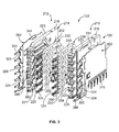
- FIG. 3 is an exploded view of one of the contact modules 122.
- the contact module 122 includes a right sub-assembly 210 and a left sub-assembly 212 that are coupled together to form the contact module 122.
- the right and left sub-assemblies 210, 212 may be mirrored halves that are coupled together to from the contact module 122.
- the right and left sub-assemblies 210, 212 include right and left conductive shells 216, 218.
- the right and left conductive shells 216, 218 may be referred to as right and left shell members 216, 218.
- the shell members 216, 218 form the conductive shell 214 when assembled.
- the shell members 216, 218 hold respective right and left frame assemblies 230, 232, which house the receptacle signal contacts 124.
- the right and left sub-assemblies also include the right and left ground shields 200, 202.
- the ground shields 200, 202 attach to respective shell members 216, 218, and the combination defines a significant portion of the shield structure 126 of the receptacle assembly 102 (shown in Figure 1 ).
- the right and left shell members 216, 218 are fabricated from a conductive material.
- the shell members 216, 218 may be die-cast from a metal material.
- the shell members 216, 218 may be stamped and formed or may be fabricated from a plastic material that has been metalized or coated with a metallic layer.
- the shell members 216, 218 may provide electrical shielding for the receptacle assembly 102.
- the right and left shell members 216, 218 include tabs 220, 221 extending inward from side walls 222, 223 thereof.
- the right tabs 220 define channels 224 therebetween, and the left tabs 221 define channels 225 therebetween.
- the receptacle signal contacts 124 of the right and left frame assemblies 230, 232 are received in corresponding channels 224, 225.
- the tabs 220, 221 provide shielding around the corresponding receptacle signal contacts 124.
- the shell members 216, 218 include grooves 360, 362 located between the channels 224, 225 at the front 226 of the conductive shell 214.
- the grooves 360, 362 are configured to receive portions of the commoning clips 402 (shown in Figure 2 ) to mechanically and electrically connect the commoning clips 402 to the shell members 216, 218.
- the right and left frame assemblies 230, 232 each include a dielectric frame 240, 242 that surrounds the respective receptacle signal contacts 124.
- the receptacle signal contacts 124 are initially held together as lead frames (not shown), which are overmolded with dielectric material to form the dielectric frames 240, 242.
- Other manufacturing processes may be utilized to form the contact modules 122 other than overmolding a lead frame, such as loading receptacle signal contacts 124 into a formed dielectric body.
- the receptacle signal contacts 124 have mating portions 250 extending from the front of the dielectric frames 240, 242 and contact tails 252 extending from the bottom of the dielectric frames 240, 242.
- the mating portions 250 and contact tails 252 are the portions of the receptacle signal contacts 124 that are configured to be coupled to the header signal contacts 144 (shown in Figure 1 ) and the circuit board 106 (shown in Figure 1 ), respectively.
- the mating portions 250 extend generally perpendicular with respect to the contact tails 252. Inner portions or encased portions of the receptacle signal contacts 124 transition between the mating portions 250 and the contact tails 252 within the dielectric frames 240, 242.
- the right frame assembly 230 is coupled to the right shell member 216.
- the right frame assembly 230 is received in corresponding channels 224 of the right shell member 216.
- the right tabs 220 extend through the right frame assembly 230 such that the tabs 220 are positioned between adjacent receptacle signal contacts 124.
- the right ground shield 200 is coupled to the right shell member 216, such as using mounting tabs 314.
- the left frame assembly 232 is coupled to the left shell member 218 with the left tabs 221 extending through the left frame assembly 232 to provide shielding between the receptacle signal contacts 124.
- the left ground shield 202 is coupled to the left shell member 218, such as using mounting tabs 344.
- the right and left sub assemblies 210, 212 are coupled together, such as by pressing dowels or pins into openings to hold the shell members 216, 218 together.
- the commoning clips 402 (shown in Figure 2 ) may be used to additionally hold the shell members 216, 218 together.
- the shell members 216, 218 provide shielding from electromagnetic interference (EMI) and/or radio frequency interference (RFI).
- EMI electromagnetic interference
- RFID radio frequency interference
- the shell members 216, 218 may provide shielding from other types of interference as well.
- the shell members 216, 218 provide shielding around the outside of the frames 240, 242, and thus around the outside of all of the receptacle signal contacts 124, such as between pairs of receptacle signal contacts 124, as well as between adjacent pairs of the receptacle signal contacts 124 using the tabs 220, 221 to control electrical characteristics, such as impedance control, cross-talk control, and the like, of the receptacle signal contacts 124.
- the grounding fingers 303 are vertically spaced from each other along the front 304 of the ground shield 200.
- the grounding fingers 303 may extend along the sides of the receptacle signal contacts 124.
- the grounding fingers 303 may provide shielding between the receptacle signal contacts 124 and receptacle signal contacts 124 of an adjacent contact module 122 held in the receptacle assembly 102.
- the grounding fingers 303 may be generally vertically aligned with receptacle signal contacts 124 in a corresponding row of the receptacle signal contacts 124.
- the grounding fingers 303 may be vertically offset, such as below, the receptacle signal contacts 124.
- each grounding finger 303 is a landing pad 324 along the exterior side of the right ground shield 200.
- the commoning clip 402 shown in Figure 2
- the commoning clip 402 engages the landing pad 324 to electrically connect the commoning clip 402 to the right ground shield 200.
- the right ground shield 200 includes a plurality of ground pins 316 extending from the bottom of the right ground shield 200.
- the ground pins 316 are configured to be terminated to the circuit board 106 (shown in Figure 1 ).
- the ground pins 316 may be compliant pins, such as eye-of-the-needle pins, that are through-hole mounted to plated vias in the circuit board 106.
- Other types of termination means or features may be provided in alternative embodiments to couple the right ground shield 200 to the circuit board 106.
- the left ground shield 202 may be similar to the right ground shield 200.
- the grounding fingers 333 are vertically spaced from each other along the front 334 of the left ground shield 202.
- the grounding fingers 333 may extend along the sides of the receptacle signal contacts 124.
- the grounding fingers 333 may provide shielding between the receptacle signal contacts 124 and receptacle signal contacts 124 of an adjacent contact module 122 held in the receptacle assembly 102.
- the grounding fingers 333 may be generally vertically aligned with receptacle signal contacts 124 in a corresponding row of the receptacle signal contacts 124. Alternatively, the grounding fingers 333 may be vertically offset, such as below, the receptacle signal contacts 124.
- each grounding finger 333 is a landing pad 325 along the exterior side of the left ground shield 202.
- the commoning clip 402 shown in Figure 2
- the commoning clip 402 engages the landing pad 325 to electrically connect the commoning clip 402 to the left ground shield 202.
- the left ground shield 202 includes a plurality of ground pins 346 extending from the bottom of the left ground shield 202.
- the ground pins 346 are configured to be terminated to the circuit board 106 (shown in Figure 1 ).
- the ground pins 346 may be compliant pins, such as eye-of-the-needle pins, that are through-hole mounted to plated vias in the circuit board 106.
- Other types of termination means or features may be provided in alternative embodiments to couple the left ground shield 202 to the circuit board 106.
- FIG 4 is an assembled perspective view of the contact module 122 shown in Figure 3 .
- the dielectric frames 240, 242 (shown in Figure 3 ) are received in the corresponding shell members 216, 218.
- the shell members 216, 218 are coupled together and generally surround the dielectric frames 240, 242.
- Right interior walls 234 of the right shell member 216 align with left interior walls 235 of the left shell member 216 at the front of the conductive shell 214 at multiple interfaces that define a seam 219.
- the seam 219 extends vertically at the interface between the right and left sub-assemblies 210, 212.
- the dielectric frames 240, 242 are aligned adjacent one another such that the receptacle signal contacts 124 are aligned with one another and define contact pairs 390.
- Each contact pair 390 is received in corresponding channels 224, 225 of the shell members 216, 218.
- Each contact pair 390 is configured to transmit differential signals through the contact module 122.
- the receptacle signal contacts 124 within each contact pair 390 are arranged in rows that extend along row axes 392.
- the receptacle signal contacts 124 within each dielectric frame 240, 242 are arranged in columns along column axes 394.
- the right and left ground shields 200, 202 are coupled to the conductive shell 214 to provide additional shielding for the receptacle signal contacts 124.
- the right ground shield 200 is positioned exterior of, and along, the right shell member 216.
- the left ground shield 202 is positioned exterior of, and along, the left shell member 218.
- the shield grounding beams 302, 332 extend into the lower row of grooves 360, 362 and are generally aligned with the receptacle contact mating portions 250 along the column axes 394.
- the grounding fingers 303, 333 extend forward from the front 226 of the conductive shell 214.
- the grounding fingers 303, 333 are generally aligned with the mating portions 250 along the row axes 392.
- the right and left ground shields 200, 202 are configured to be electrically connected to the header shields 146 (shown in Figure 1 ) when the receptacle assembly 102 is coupled to the header assembly 104 (both shown in Figure 1 ).
- FIG 5 is a perspective view of the commoning clip 402.
- the commoning clip 402 couples to multiple contact modules 122 (shown in Figure 4 ) to mechanically and electrically couple the contact modules 122 together.
- the commoning clip 402 includes openings 406 located along a rear 408 thereof for coupling to the conductive shells 214 (shown in Figure 4 ) of each contact module 122.
- the clip grounding beams 404 extend forward from a front 410 of the commoning clip 402 for electrical connection to header shields 146 (shown in Figure 1 ) of the header assembly 104 (shown in Figure 1 ).
- multiple commoning clips 402 are used to provide shielding and electrically connect the contact modules 122.
- the commoning clip 402 is fabricated from a conductive material.
- the commoning clip 402 may be stamped and formed from a metal sheet.
- the commoning clip 402 has a generally planar main body 412.
- the clip grounding beams 404 may be stamped and then bent during the forming process out of plane with respect to the main body 412.
- the commoning clip 402 may provide electrical shielding for the receptacle assembly 102 (shown in Figure 1 ).
- the commoning clip 402 is formed as one piece, so the electrical connections between the header shields 146 and the clip grounding beams 404 are commoned across all contact modules 122.
- the rear 408 of the commoning clip 402 couples to the contact modules 122.
- the openings 406 are spaced along the length of the commoning clip 402.
- the openings 406 include barbs 414 along sides of the openings 406 that extend into the openings 406.
- the barbs 414 face each other across the opening 406.
- the barbs 414 reduce the width of the opening 406 and are used to provide an interference fit when coupled to the contact modules 122.
- the rear 408 of the commoning clip 402 may include dimples 416 which extend above and/or below the plane of the main body 412. The dimples 416 may be located near the openings 406 .
- the commoning clip 402 includes shield fingers 418 extending from the rear 408 thereof.
- the shield fingers 418 may be compliant pins, such as eye-of-the-needle pins, and will be referred to hereinafter as pins 418.
- the pins 418 are horizontally spaced along the length of the commoning clip 402.
- the pins 418 may be generally coplanar with the main body 412.
- the pins 418 are positioned between adjacent openings 406 in specified locations such that when the commoning clip 402 is loaded into the contact modules 122, each pin 418 engages right and left ground shields 200, 202 of adjacent contact modules 122 (shown in Figure 6 ).
- the pins 418 may engage the ground shields 200, 202 by an interference fit.
- the commoning clip 402 includes a jumper region 420 between openings 406 at the rear 408 and the clip grounding beams 404 at the front 410.
- the jumper region 420 physically connects the regions of the commoning clip 402 together.
- the jumper region 420 electrically connects and commons the grounding beams 404 and pins 418 together.
- the clip grounding beams 404 each have a mating interface 422 at a distal end thereof.
- the mating interface 422 is configured to engage the corresponding header shield 146 (shown in Figure 1 ).
- FIG 6 is an enlarged view of a top corner portion of the receptacle assembly 102 with the housing 120 (shown in Figure 1 ) removed.
- the commoning clips 402 are shown loaded into the stack 121 of contact modules 122.
- the commoning clip 402 extends horizontally across all of the contact modules 122 in the receptacle assembly 102.
- commoning clips that extend across only one contact module 122 may be used, such as to electrically connect the shell members 216, 218 together.
- the commoning clip 402 is inserted into the grooves 360, 362 of the shell members 216, 218 until the commoning clip 402 contacts the interior walls 234, 235 of the shell members 216, 218.
- the dimples 416 are loaded into the grooves 360, 362 and engage inner walls of the grooves 360, 362 to create an interference fit between the commoning clip 402 and the shell members 216, 218.
- the dimples 416 stabilize the commoning clip 402 and prohibit unintentional disengagement of the commoning clip 402 from the contact modules 122. Electrical connections are defined between the commoning clip 402 at the dimples 416 and each of the shell members 216, 218.
- the interior walls 234, 235 of the shell members 216, 218 are received in corresponding openings 406.
- the interior walls 234, 235 are pinched together at the seam 219 by the barbs 414 (shown in Figure 5 ).
- the interior walls 234, 235 enter the openings 406 and the barbs 414 engage the interior walls 234, 235 by an interference fit.
- the barbs 414 force the interior wall 234 towards the interior wall 235 and vice-versa, pinching the interior walls 234, 235 together at the seam 219.
- the openings 406 and barbs 414 hold the right and left sub-assemblies 210, 212 of each contact module 122 together.
- the pins 418 When assembled, the pins 418 extend between the right ground shield 200 of one contact module 122 and the left ground shield 202 of the adjacent contact module 122. The pins 418 engage corresponding landing pads 324, 325 of the ground shields 200, 202. The compliant design of the pins 418 pushes the ground shields 200, 202 against the shell members 216, 218, helping to squeeze the shell members 216, 218 together. Electrical connections are defined between the commoning clip 402 at the pins 418, and each of the ground shields 200, 202. The eye-of-the-needle design applies a force to the ground shields 200, 202 towards the respective conductive shell members 216, 218.
- the pin 418 will push the right ground shield 200 of one contact module 122 toward the corresponding right shell member 216, while simultaneously pushing the left ground shield 202 of the adjacent contact module 122 toward the corresponding left shell member 218.
- the pins 418 thus force the ground shields 200, 202 against the shell members 216, 218 to hold the conductive shells 214 together and to force the ground shields 200, 202 into direct electrical contact with the conductive shell 214.
- the jumper regions 420 are positioned forward of, and extend across, the front 226 of the shell members 216, 218.
- the jumper regions 420 and grounding beams 404 extend vertically above and/or below the signal contact pairs 390.
- the grounding beams 404 are generally aligned in column with corresponding receptacle signal contacts 124 of the receptacle signal contact pairs 390.
- each contact pair 390 will be shielded above and below by corresponding clip grounding beams 404.
- right and left grounding fingers 303, 333 of the right and left ground shields 200, 202 shield each contact pair 390 on the sides.
- each contact pair 390 is substantially shielded on all four sides to reduce electrical interference in the signal connection.
- the right and left ground shields 200, 202 and the commoning clips 402 provide shielding between the contact pairs 390 even when the receptacle assembly 102 is partially unmated or not fully mated with the header assembly 104.
- Figure 7 is a cross-sectional view of a portion of the receptacle assembly 102.
- the commoning clips 402 when the commoning clips 402 are coupled to the contact modules 122, the commoning clips 402 enter the grooves 360, 362 of the shell members 216, 218.
- the interior walls 234, 235 of the shell members 216, 218 are received in the openings 406.
- the openings 406 are sized such that the interior walls 234, 235 are forced against each other at the seam 219 in order to fit within the openings 406.
- the barbs 414 shown in Figure 5
- the inner walls of the openings 406 provide additional points of contact with the interior walls 234, 235 and provide additional force on the interior walls 234, 235 towards each other.
- the dimples 416 on the commoning clip 402 engage the inner walls of the grooves 360, 362.
- the dimples 416 engage the inner walls of the grooves 360, 362 by an interference fit which stabilizes the commoning clip 402 relative to the contact modules 122 and prohibits unintentional removal therefrom.
- the receptacle signal contact pairs 390 are housed in the channels 224, 225 of the right and left shell members 216, 218. Along the outer side of the shell members 216, 218 are the ground fingers 303, 333.
- FIG 8 is a rear perspective view of a portion of the receptacle assembly 102 with two contact modules 122 thereof removed for clarity.
- the front housing 120 includes a rear side 440 configured to receive the contact modules 122 therein.
- the rear side 440 includes multiple vertical ribs 442.
- the vertical ribs 442 are spaced from each other and define multiple cavities 444 therebetween that are configured to receive individual contact modules 122.
- the vertical ribs 442 include multiple slots 446 that hold the commoning clips 402 within the front housing 120.
- the commoning clips 402 are coupled to each of the contact modules 122 prior to loading the commoning clips 402 and contact modules 122 into the front housing 120.
- the commoning clips 402 may be first loaded individually into the slots 446 of the front housing 120.
- the contact modules 122 may be loaded individually into the cavities 444, where upon doing so the contact modules 122 engage the preloaded commoning clips 402.
- the clip grounding beams 404 When assembled, the clip grounding beams 404 (shown in Figure 5 ) extend into the ground contact openings 134 (shown in Figure 1 ) in the front housing 120 for mating with the header shields 146 (shown in Figure 1 ) of the header assembly 104 (shown in Figure 1 ).
- FIG 9 is a perspective view of a commoning clip 502 formed in accordance with an exemplary embodiment.
- the commoning clip 502 may be similar to the commoning clip 402 (shown in Figures 2 and 5-8 ) in some respects.
- the commoning clip 502 includes a main body 512 with a rear 508 and a front 510.
- the front 510 of the commoning clip 502 includes a jumper region 520 and clip grounding beams 504 extending forward therefrom.
- the rear 508 of the main body 512 defines openings 506, and barbs 514 extend into the openings 506. Dimples 516 extend above and/or below the plane of the main body 512.
- the commoning clip 502 also includes a plurality of shield fingers 530 extending from the rear 508 thereof.
- the shield fingers 530 may be shaped like tuning forks, and will be referred to hereinafter as tuning fork contacts 530.
- the tuning fork contacts 530 may be generally planar with the main body 512.
- Each tuning fork contact 530 includes a right tine 532 and a left tine 534. The right and left tines 532, 534 define a slot 536 therebetween.
- the tuning fork contacts 530 are mounted in pairs 538 between the openings 506 and aligned such that one tuning fork contact 530 receives and engages the right ground shield 200 (shown in Figure 2 ) of one contact module 122 (shown in Figure 2 ), and the other tuning fork contact 530 in the pair 538 receives and engages the left ground shield 202 (shown in Figure 2 ) of the adjacent contact module 122.
- Each tuning fork contact 530 receives the front 304, 334 of a respective ground shield 200, 202 within the slot 536.
- the ground shields 200, 202 are held by an interference fit within the slots 536 of the tuning fork contacts 530.
Applications Claiming Priority (1)
| Application Number | Priority Date | Filing Date | Title |
|---|---|---|---|
| US13/685,449 US8777663B2 (en) | 2012-11-26 | 2012-11-26 | Receptacle assembly having a commoning clip with grounding beams |
Publications (1)
| Publication Number | Publication Date |
|---|---|
| EP2736126A1 true EP2736126A1 (en) | 2014-05-28 |
Family
ID=49626877
Family Applications (1)
| Application Number | Title | Priority Date | Filing Date |
|---|---|---|---|
| EP13194479.5A Withdrawn EP2736126A1 (en) | 2012-11-26 | 2013-11-26 | Grounding structures for receptacle assembly |
Country Status (4)
| Country | Link |
|---|---|
| US (1) | US8777663B2 (zh) |
| EP (1) | EP2736126A1 (zh) |
| CN (1) | CN103840320B (zh) |
| TW (1) | TWI621310B (zh) |
Cited By (2)
| Publication number | Priority date | Publication date | Assignee | Title |
|---|---|---|---|---|
| WO2015164201A1 (en) * | 2014-04-22 | 2015-10-29 | Tyco Electronics Corporation | Mezzanine connector assembly |
| CN114582665A (zh) * | 2022-01-29 | 2022-06-03 | 上海京硅智能技术有限公司 | 隔离开关触头极 |
Families Citing this family (28)
| Publication number | Priority date | Publication date | Assignee | Title |
|---|---|---|---|---|
| JP5878071B2 (ja) * | 2012-04-13 | 2016-03-08 | タイコエレクトロニクスジャパン合同会社 | 電気コネクタ |
| US9054467B2 (en) * | 2013-10-11 | 2015-06-09 | Tyco Electronics Corporation | Electrical connector having a connector shroud |
| CN105470736B (zh) * | 2014-08-27 | 2019-08-30 | 富士康(昆山)电脑接插件有限公司 | 电连接器 |
| US20160149362A1 (en) * | 2014-11-21 | 2016-05-26 | Tyco Electronics Corporation | Connector brick for cable communication system |
| US9570857B2 (en) * | 2015-03-27 | 2017-02-14 | Tyco Electronics Corporation | Electrical connector and interconnection system having resonance control |
| US9425556B1 (en) | 2015-07-17 | 2016-08-23 | Tyco Electronics Corporation | Interconnection system and an electrical connector having resonance control |
| CN205070057U (zh) * | 2015-07-31 | 2016-03-02 | 富士康(昆山)电脑接插件有限公司 | 电连接器 |
| US9431771B1 (en) * | 2015-11-04 | 2016-08-30 | Delphi Technologies, Inc | Electromagnetically shielded connector system |
| JP6718961B2 (ja) * | 2015-12-14 | 2020-07-08 | モレックス エルエルシー | 接地シールドを省略するバックプレーンコネクタ、及びそれを使用するシステム |
| US10128616B2 (en) * | 2016-07-25 | 2018-11-13 | Te Connectivity Corporation | Electrical connector having commoned ground shields |
| US9831608B1 (en) * | 2016-10-31 | 2017-11-28 | Te Connectivity Corporation | Electrical connector having ground shield that controls impedance at mating interface |
| US9812817B1 (en) | 2017-01-27 | 2017-11-07 | Te Connectivity Corporation | Electrical connector having a mating connector interface |
| US10128619B2 (en) | 2017-01-27 | 2018-11-13 | Te Connectivity Corporation | Ground shield for a contact module |
| US9917406B1 (en) * | 2017-01-27 | 2018-03-13 | Te Connectivity Corporation | Shielding structure for a contact module having a ground clip |
| US9923309B1 (en) | 2017-01-27 | 2018-03-20 | Te Connectivity Corporation | PCB connector footprint |
| US10186810B2 (en) | 2017-01-27 | 2019-01-22 | Te Connectivity Corporation | Shielding structure for a contact module |
| US10186811B1 (en) * | 2017-12-06 | 2019-01-22 | Te Connectivity Corporation | Shielding for connector assembly |
| US10790618B2 (en) * | 2018-01-30 | 2020-09-29 | Te Connectivity Corporation | Electrical connector system having a header connector |
| US10566740B2 (en) * | 2018-03-29 | 2020-02-18 | Te Connectivity Corporation | Shielding structure for a contact module of an electrical connector |
| TWI668927B (zh) * | 2018-04-03 | 2019-08-11 | 慶良電子股份有限公司 | 電連接器及其傳輸片 |
| US10756492B2 (en) | 2018-09-18 | 2020-08-25 | Te Connectivity Corporation | Shielding structure for an electrical connector |
| US10574000B1 (en) * | 2018-11-05 | 2020-02-25 | Te Connectivity Corporation | Grounding structure for an electrical connector |
| US10763622B2 (en) * | 2018-11-05 | 2020-09-01 | Te Connectivity Corporation | Grounding structure for an electrical connector |
| US10686282B1 (en) * | 2019-02-27 | 2020-06-16 | Te Connectivity Corporation | Electrical connector for mitigating electrical resonance |
| CN111668663A (zh) * | 2019-03-05 | 2020-09-15 | 庆虹电子(苏州)有限公司 | 电连接器总成、母端连接器、及公端连接器 |
| CN113131265B (zh) * | 2019-12-31 | 2023-05-19 | 富鼎精密工业(郑州)有限公司 | 电连接器 |
| CN112134097B (zh) * | 2020-10-09 | 2022-03-15 | 东莞立讯技术有限公司 | 电连接器 |
| CN113193407B (zh) * | 2021-02-02 | 2022-10-25 | 中山得意电子有限公司 | 电连接器 |
Citations (3)
| Publication number | Priority date | Publication date | Assignee | Title |
|---|---|---|---|---|
| WO2000010233A2 (en) * | 1998-08-12 | 2000-02-24 | Robinson Nugent, Inc. | Connector apparatus |
| EP2390961A1 (en) * | 2010-05-28 | 2011-11-30 | Tyco Electronics Corporation | Connector assembly |
| US8262412B1 (en) * | 2011-05-10 | 2012-09-11 | Tyco Electronics Corporation | Electrical connector having compensation for air pockets |
Family Cites Families (14)
| Publication number | Priority date | Publication date | Assignee | Title |
|---|---|---|---|---|
| US6231391B1 (en) * | 1999-08-12 | 2001-05-15 | Robinson Nugent, Inc. | Connector apparatus |
| US6347962B1 (en) * | 2001-01-30 | 2002-02-19 | Tyco Electronics Corporation | Connector assembly with multi-contact ground shields |
| JP3831333B2 (ja) * | 2002-11-13 | 2006-10-11 | 第一電子工業株式会社 | 電気コネクタ |
| US7513797B2 (en) * | 2004-02-27 | 2009-04-07 | 3M Innovative Properties Company | Connector apparatus |
| CN101459299B (zh) * | 2007-12-11 | 2010-11-17 | 富士康(昆山)电脑接插件有限公司 | 电连接器 |
| US8157591B2 (en) | 2008-12-05 | 2012-04-17 | Tyco Electronics Corporation | Electrical connector system |
| US7988491B2 (en) * | 2009-12-11 | 2011-08-02 | Tyco Electronics Corporation | Electrical connector having contact modules |
| US7976340B1 (en) | 2010-03-12 | 2011-07-12 | Tyco Electronics Corporation | Connector system with electromagnetic interference shielding |
| US8157595B2 (en) | 2010-07-13 | 2012-04-17 | Tyco Electronics Corporation | Ground shield for an electrical connector |
| US8221139B2 (en) | 2010-09-13 | 2012-07-17 | Tyco Electronics Corporation | Electrical connector having a ground clip |
| US8398432B1 (en) * | 2011-11-07 | 2013-03-19 | Tyco Electronics Corporation | Grounding structures for header and receptacle assemblies |
| US8500487B2 (en) * | 2011-11-15 | 2013-08-06 | Tyco Electronics Corporation | Grounding structures for header and receptacle assemblies |
| US8419472B1 (en) * | 2012-01-30 | 2013-04-16 | Tyco Electronics Corporation | Grounding structures for header and receptacle assemblies |
| US8579636B2 (en) * | 2012-02-09 | 2013-11-12 | Tyco Electronics Corporation | Midplane orthogonal connector system |
-
2012
- 2012-11-26 US US13/685,449 patent/US8777663B2/en not_active Expired - Fee Related
-
2013
- 2013-11-20 TW TW102142217A patent/TWI621310B/zh not_active IP Right Cessation
- 2013-11-26 CN CN201310757376.2A patent/CN103840320B/zh not_active Expired - Fee Related
- 2013-11-26 EP EP13194479.5A patent/EP2736126A1/en not_active Withdrawn
Patent Citations (3)
| Publication number | Priority date | Publication date | Assignee | Title |
|---|---|---|---|---|
| WO2000010233A2 (en) * | 1998-08-12 | 2000-02-24 | Robinson Nugent, Inc. | Connector apparatus |
| EP2390961A1 (en) * | 2010-05-28 | 2011-11-30 | Tyco Electronics Corporation | Connector assembly |
| US8262412B1 (en) * | 2011-05-10 | 2012-09-11 | Tyco Electronics Corporation | Electrical connector having compensation for air pockets |
Cited By (4)
| Publication number | Priority date | Publication date | Assignee | Title |
|---|---|---|---|---|
| WO2015164201A1 (en) * | 2014-04-22 | 2015-10-29 | Tyco Electronics Corporation | Mezzanine connector assembly |
| US9312643B2 (en) | 2014-04-22 | 2016-04-12 | Tyco Electronics Corporation | Mezzanine connector assembly |
| CN114582665A (zh) * | 2022-01-29 | 2022-06-03 | 上海京硅智能技术有限公司 | 隔离开关触头极 |
| CN114582665B (zh) * | 2022-01-29 | 2024-03-12 | 上海京硅智能技术有限公司 | 隔离开关触头极 |
Also Published As
| Publication number | Publication date |
|---|---|
| CN103840320A (zh) | 2014-06-04 |
| TW201440338A (zh) | 2014-10-16 |
| CN103840320B (zh) | 2017-10-20 |
| TWI621310B (zh) | 2018-04-11 |
| US20140148054A1 (en) | 2014-05-29 |
| US8777663B2 (en) | 2014-07-15 |
Similar Documents
| Publication | Publication Date | Title |
|---|---|---|
| US8777663B2 (en) | Receptacle assembly having a commoning clip with grounding beams | |
| US8398431B1 (en) | Receptacle assembly | |
| US8905786B2 (en) | Header connector for an electrical connector system | |
| US10276984B2 (en) | Connector assembly having a pin organizer | |
| US8444434B2 (en) | Grounding structures for header and receptacle assemblies | |
| US8419472B1 (en) | Grounding structures for header and receptacle assemblies | |
| US8475209B1 (en) | Receptacle assembly | |
| US8500487B2 (en) | Grounding structures for header and receptacle assemblies | |
| US8591260B2 (en) | Grounding structures for header and receptacle assemblies | |
| US10186811B1 (en) | Shielding for connector assembly | |
| US9985389B1 (en) | Connector assembly having a pin organizer | |
| US8430691B2 (en) | Grounding structures for header and receptacle assemblies | |
| US8662924B2 (en) | Electrical connector system having impedance control | |
| JP6369850B2 (ja) | リセプタクル組立体用接地構造体 | |
| US8398432B1 (en) | Grounding structures for header and receptacle assemblies | |
| US9812817B1 (en) | Electrical connector having a mating connector interface | |
| US8597052B2 (en) | Grounding structures for header and receptacle assemblies | |
| US10476210B1 (en) | Ground shield for a contact module | |
| US11005218B2 (en) | Shielding structure for an electrical connector | |
| US10868392B2 (en) | Ground commoning conductors for electrical connector assemblies | |
| US11283222B2 (en) | Contact module for a header assembly |
Legal Events
| Date | Code | Title | Description |
|---|---|---|---|
| PUAI | Public reference made under article 153(3) epc to a published international application that has entered the european phase |
Free format text: ORIGINAL CODE: 0009012 |
|
| 17P | Request for examination filed |
Effective date: 20131126 |
|
| AK | Designated contracting states |
Kind code of ref document: A1 Designated state(s): AL AT BE BG CH CY CZ DE DK EE ES FI FR GB GR HR HU IE IS IT LI LT LU LV MC MK MT NL NO PL PT RO RS SE SI SK SM TR |
|
| AX | Request for extension of the european patent |
Extension state: BA ME |
|
| STAA | Information on the status of an ep patent application or granted ep patent |
Free format text: STATUS: THE APPLICATION IS DEEMED TO BE WITHDRAWN |
|
| 18D | Application deemed to be withdrawn |
Effective date: 20141129 |