EP2736084A1 - Avalanche photodetector element with increased electric field strength - Google Patents
Avalanche photodetector element with increased electric field strength Download PDFInfo
- Publication number
- EP2736084A1 EP2736084A1 EP12193767.6A EP12193767A EP2736084A1 EP 2736084 A1 EP2736084 A1 EP 2736084A1 EP 12193767 A EP12193767 A EP 12193767A EP 2736084 A1 EP2736084 A1 EP 2736084A1
- Authority
- EP
- European Patent Office
- Prior art keywords
- doped regions
- doped
- semiconducting material
- avalanche
- avalanche photodetector
- Prior art date
- Legal status (The legal status is an assumption and is not a legal conclusion. Google has not performed a legal analysis and makes no representation as to the accuracy of the status listed.)
- Granted
Links
Images




Classifications
-
- H—ELECTRICITY
- H10—SEMICONDUCTOR DEVICES; ELECTRIC SOLID-STATE DEVICES NOT OTHERWISE PROVIDED FOR
- H10F—INORGANIC SEMICONDUCTOR DEVICES SENSITIVE TO INFRARED RADIATION, LIGHT, ELECTROMAGNETIC RADIATION OF SHORTER WAVELENGTH OR CORPUSCULAR RADIATION
- H10F30/00—Individual radiation-sensitive semiconductor devices in which radiation controls the flow of current through the devices, e.g. photodetectors
- H10F30/20—Individual radiation-sensitive semiconductor devices in which radiation controls the flow of current through the devices, e.g. photodetectors the devices having potential barriers, e.g. phototransistors
- H10F30/21—Individual radiation-sensitive semiconductor devices in which radiation controls the flow of current through the devices, e.g. photodetectors the devices having potential barriers, e.g. phototransistors the devices being sensitive to infrared, visible or ultraviolet radiation
- H10F30/22—Individual radiation-sensitive semiconductor devices in which radiation controls the flow of current through the devices, e.g. photodetectors the devices having potential barriers, e.g. phototransistors the devices being sensitive to infrared, visible or ultraviolet radiation the devices having only one potential barrier, e.g. photodiodes
- H10F30/225—Individual radiation-sensitive semiconductor devices in which radiation controls the flow of current through the devices, e.g. photodetectors the devices having potential barriers, e.g. phototransistors the devices being sensitive to infrared, visible or ultraviolet radiation the devices having only one potential barrier, e.g. photodiodes the potential barrier working in avalanche mode, e.g. avalanche photodiodes
-
- H—ELECTRICITY
- H10—SEMICONDUCTOR DEVICES; ELECTRIC SOLID-STATE DEVICES NOT OTHERWISE PROVIDED FOR
- H10F—INORGANIC SEMICONDUCTOR DEVICES SENSITIVE TO INFRARED RADIATION, LIGHT, ELECTROMAGNETIC RADIATION OF SHORTER WAVELENGTH OR CORPUSCULAR RADIATION
- H10F77/00—Constructional details of devices covered by this subclass
- H10F77/10—Semiconductor bodies
- H10F77/12—Active materials
- H10F77/122—Active materials comprising only Group IV materials
-
- H—ELECTRICITY
- H10—SEMICONDUCTOR DEVICES; ELECTRIC SOLID-STATE DEVICES NOT OTHERWISE PROVIDED FOR
- H10F—INORGANIC SEMICONDUCTOR DEVICES SENSITIVE TO INFRARED RADIATION, LIGHT, ELECTROMAGNETIC RADIATION OF SHORTER WAVELENGTH OR CORPUSCULAR RADIATION
- H10F77/00—Constructional details of devices covered by this subclass
- H10F77/10—Semiconductor bodies
- H10F77/14—Shape of semiconductor bodies; Shapes, relative sizes or dispositions of semiconductor regions within semiconductor bodies
- H10F77/148—Shapes of potential barriers
-
- H—ELECTRICITY
- H10—SEMICONDUCTOR DEVICES; ELECTRIC SOLID-STATE DEVICES NOT OTHERWISE PROVIDED FOR
- H10F—INORGANIC SEMICONDUCTOR DEVICES SENSITIVE TO INFRARED RADIATION, LIGHT, ELECTROMAGNETIC RADIATION OF SHORTER WAVELENGTH OR CORPUSCULAR RADIATION
- H10F77/00—Constructional details of devices covered by this subclass
- H10F77/20—Electrodes
- H10F77/206—Electrodes for devices having potential barriers
-
- Y—GENERAL TAGGING OF NEW TECHNOLOGICAL DEVELOPMENTS; GENERAL TAGGING OF CROSS-SECTIONAL TECHNOLOGIES SPANNING OVER SEVERAL SECTIONS OF THE IPC; TECHNICAL SUBJECTS COVERED BY FORMER USPC CROSS-REFERENCE ART COLLECTIONS [XRACs] AND DIGESTS
- Y02—TECHNOLOGIES OR APPLICATIONS FOR MITIGATION OR ADAPTATION AGAINST CLIMATE CHANGE
- Y02E—REDUCTION OF GREENHOUSE GAS [GHG] EMISSIONS, RELATED TO ENERGY GENERATION, TRANSMISSION OR DISTRIBUTION
- Y02E10/00—Energy generation through renewable energy sources
- Y02E10/50—Photovoltaic [PV] energy
- Y02E10/547—Monocrystalline silicon PV cells
Definitions
- the current disclosure relates to an avalanche photodetector for converting an optical signal to an electrical signal according to the preamble of the first claim.
- the present disclosure also relates to use of such avalanche photodetector and a method for making such a avalanche photodetector.
- the known avalanche photodetector element comprises an absorbing intrinsic semiconducting material with bandgap smaller than photon energy of the to-be-detected light wave, including Group IV semiconductors such as Germanium (Ge), Silicon-Germanium (SiGe), Germanium Tin (GeSn) or SiGeSn alloys, or alternatively, binary, ternary and quaternary III-V semiconductors, including but not limited to InP, InGaAs, InGaAsP and related materials.
- Group IV semiconductors such as Germanium (Ge), Silicon-Germanium (SiGe), Germanium Tin (GeSn) or SiGeSn alloys, or alternatively, binary, ternary and quaternary III-V semiconductors, including but not limited to InP, InGaAs, InGaAsP and related materials.
- Light with infrared wavelengths can be coupled directly from free space into the absorbing semiconductor, or alternatively, can be guided and coupled into the absorbing semiconductor by means of an optically transparent input waveguide, which can be built from optically transparent semiconductors such as silicon.
- the absorbing semiconducting material comprises a p-doped region, an n-doped region, and an intrinsic region in between the doped regions. A schematic overview of such configuration is for example shown in figure 1 .
- the p-doped , the n-doped and the intrinsic region are preferably implemented longitudinally along the propagation direction of the incoming light wave and extend with their longitudinal direction parallel to each other and parallel to the longitudinal direction of the absorbing material.
- the doped regions and the intrinsic semiconducting material thus form a PIN-junction photodiode wherein the input waveguide, if present, and the intrinsic semiconducting material are arranged with respect to each other such that optical waves, with typical infrared wavelengths greater than 1200nm, guided by the input waveguide are substantially coupled into the intrinsic semiconducting material to the so called PIN-junction, formed by the combination of a p-doped region, an n-doped region and the intrinsic semiconducting material in between them, forming a PIN photodiode.
- a reverse bias potential difference is applied between the p-doped region and the n-doped region, resulting in an electric field in the intrinsic region.
- the optical signal is converted to an electrical signal by optical excitation of electrons from the valence band to the conduction band under influence of the optical waves, essentially forming free electrons and free holes in the semiconducting material, which are subsequently collected at the n-doped region and p-doped region respectively, under the influence of the internal electric field.
- the generated free electrons or the generated free holes, or both can be multiplied by the mechanism known as impact ionization, essentially creating an avalanche of free electrons and/or holes.
- impact ionization essentially creating an avalanche of free electrons and/or holes.
- Such resulting multiplication gain essentially improves the responsiveness of the photodiode, potentially resulting in superior sensitivity of optical receivers built from such avalanche photodetectors.
- the semiconducting material comprises at least one array of p-doped regions or n-doped regions.
- the semiconducting material comprises at least one array of p-doped regions or n-doped regions on the same area as the avalanche photodetector element according to the state of the art
- the dimensions of the different doped regions of the array are much smaller than the dimensions of the longitudinally shaped doped regions according to the state of the art.
- the strength of the electric field will increase in the proximity of the doped regions without having to increase the reverse bias potential. Therefore, for example, the power required for operating the avalanche photodetector element does not need to be increased and can even be lowered with respect to the prior art avalanche photodetector element.
- the doped regions of the array of p-doped regions or n-doped regions are delimited from each other by, more preferably undoped, intrinsic semiconducting material.
- the semiconductor material is provided to absorb the optical waves of the optical signal thereby creating a electron-hole pair which are than respectively accelerated to the respective doped regions under influence of the electric field.
- the shape and position of the p-doped regions or n-doped regions of the PIN diode are implemented in such a way to locally increase the internal electric field generated by an external reverse bias applied to the diode electrodes.
- the n-doped and/or p-doped region of the PIN diode as an array of respectively n-doped and/or p-doped regions, it has been found that the electric field is enhanced compared to an implementation with only one p-type region and only one n-type region as shown in figure 1 .
- alternating p-type and n-type regions further helps to improve the electrical field. Further, it is found that the electric field improvement is increased by reducing the size of the individual contacts and individual doped regions in the array, as well as by reducing the width of the intrinsic material in between the doped regions.
- the doped regions of the array of p-doped regions or n-doped regions are less, preferably substantially less, than 0.1 micron wide. Such dimensioned doped regions have been found to generate a sufficiently large electric field in their vicinity to allow avalanche electrons to be created without having to use relatively large voltages.
- the at least one avalanche photodiode has a multiplication factor of more than one, preferably substantially greater than two, which has been found sufficient for the working of the avalanche photodetector element according to the disclosure.
- the semiconducting material comprises at least an array of p-doped regions and an array of n-doped regions forming a resulting array of doped regions. It has been found that by employing both an array of p-doped regions and b-doped regions the strength of the electric field can be further increased as both the dimensions of the p-doped region as the n-doped regions are now reduced.
- the rows and/or columns, preferably the rows and the columns, of the resulting array of doped regions are made up from p-doped regions and n-doped regions alternating each other.
- Such configuration of the different doped regions have been found to even further increase the volume of material which is susceptible to creation of optically excited electrons as some opposingly doped regions forming PIN-junction avalanche photodiodes are positioned adjacently along at least two sides of the doped regions and possible even along four sides of the doped regions when both the rows and the columns are provided with alternating p-doped regions and n-doped regions.
- adjacent doped regions are delimited from each other with a delimiting distance of 0.05 micron - 0.5 micron, preferably 0.1 micron - 0.2 micron. Such distances have been found to provide further improved avalanche photodetectors.
- the intrinsic semiconducting material comprises Germanium, Silicon-Germanium, Germanium-Tin,. It has been found that Germanium and Silicon-Germanium have good absorbing optical properties with optical waves having a wavelength of less than 1.6 micron. As such optical waves are often used for optical communication, for example over fiberglass communication lines, it has been found that such avalanche photodetectors can be used in optical communication applications. Germanium-Tin has been found to present improved absorption for wavelengths above 1.6micron.
- the input waveguide comprises Silicon, preferably substantially Silicon, most preferable is made from Silicon, as silicon has does not substantially absorb optical waves having a wavelength in the range 1.2 - 3 micron, preferably 1.3 micron - 1.6 micron which are often used in optical communications.
- the doped regions are provided with electrodes for interconnecting the avalanche photodetector in an electrical circuit.
- the disclosure also relates to an electrical circuit comprising the avalanche photodetector according to the disclosure wherein in use a reverse bias potential difference is applied over the p-doped region and the n-doped region forming the PIN-junction avalanche photodiode.
- the electrical circuit can for example be incorporated on a chip.
- the disclosure also relates to a method for making the avalanche photodetector according to the disclosure.
- the doped regions can for example be made by ion-implantation, preferably followed by annealing or selective epitaxy.
- the disclosure also relates to the use of the avalanche photodetector according to the disclosure for converting an optical signal to an electrical signal. Such use is for example especially preferred in optical communication applications.
- the optic waves have a wavelength in the range 1.2-3 micron, preferably 1.3 micron - 1.6 micron as such wavelengths are often used in optical communications applications, as discussed above.
- a reverse bias potential difference is applied over the p-doped region and the n-doped region forming the PIN-junction avalanche photodiode.
- the reverse bias potential difference is about 1V - 10V, preferably 2V - 4V as such reverse bias potential differences have been found to be quite available in for example chip applications whereas nevertheless being sufficiently high to create avalanche electrons. Good results are expected at for example 2V.
- the reverse bias is applied to the preferred electrodes discussed above.
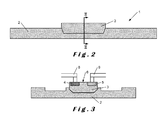
- Figure 2 shows a cross section of a side view of a avalanche photodetector element 1 for converting an optical signal to an electrical signal according to the present disclosure.
- the avalanche photodetector element 1 comprises an input waveguide 2 and an intrinsic, absorbing semiconducting material 3.
- the semiconducting material 3 comprises at least one p-doped region 4 and at least one n-doped region 5.
- the doped regions 4, 5 are not shown in figure 2
- the doped regions 4, 5 are for example shown in figure 3 .
- the doped regions 4, 5 and the intrinsic, absorbing semiconducting material 3 form at least one PIN-junction avalanche photodiode 6.
- the input waveguide 2 and the intrinsic semiconducting material 3 are arranged with respect to each other such that optical waves conducted by the input waveguide 2 are substantially conducted into the intrinsic semiconducting material 3 to the PIN-junction avalanche photodiode 6.
- the optical signal is converted to an electrical signal.
- the precise configuration, such as for example dimensions, shape, etc., of the input waveguide 2 and the intrinsic semiconducting material 3, keeping their above-described functionality in mind, is not essential for the disclosure and can be further determined by the person skilled in the art depending on for example the characteristics, such as for example wavelength, intensity, etc., of the optical waves used, the intrinsic semiconducting material 3, the material of the waveguide 2, etc.
- the disclosure also relates to an electrical circuit comprising the avalanche photodetector 1 according to the disclosure.
- a reverse bias potential difference is applied over the p-doped region 4 and the n-doped region 5 forming the PIN-junction avalanche photodiode 6.
- the semiconducting material 3 comprises at least one array of p-doped regions 4 or n-doped region 5. Different possibilities of arrays of the doped regions 4, 5 are for example shown in figures 4 - 10 .
- Figure 4 for example shows a top view of a first embodiment of part of the avalanche photodetector element 1 according to the disclosure.
- the avalanche photodetector element 1 comprises an array of n-doped regions 5. However, this is not critical for the disclosure and as shown in figure 5 , the avalanche photodetector element 1 can also comprise an array of p-doped regions 5.
- the array 4, 5 comprises at least two doped regions, but preferably more than two such as for example three, four, five, six, seven, eight, nine, ten, eleven, twelve, thirteen, fourteen, fifteen, twenty, twenty-five, thirty, thirty-five, forty, etc.
- the number of doped regions is determined in function of, for example the distance in between the doped regions along propagation direction of the optical wave and the length of the intrinsic semiconducting material 3 along that propagation direction. In general the length of the intrinsic semiconducting material 3 along that propagation direction is in the range 5 - 100 micron.
- the doped regions 4, 5 of the array of p-doped regions 4 or n-doped regions 5 are delimited from each other by undoped intrinsic semiconducting material 3.
- the array of doped regions 4, 5 is in the form of a linear array, having only a single column. Such configuration is however not critical for the disclosure, and other configurations are also possible such as for example an array having two or more columns.
- the respective p-doped region and n-doped region opposing the respective array of n-doped regions 5 or p-doped regions 4 is in the form of a single uninterrupted doped region.
- Figure 6 shows a further preferred embodiment wherein the single uninterrupted doped region is also replaced by an array of doped regions.
- the arrays of n-doped regions and p-doped regions 4, 5 form a resulting array of doped regions 7.
- the resulting array of doped regions 7 comprises two arrays of doped regions 4, 5, one n-doped region 5 and one p-doped region 4.
- the resulting array of doped regions 7 can also comprise three, four, five, six, seven, eight, nine, ten, eleven, twelve, thirteen, fourteen, fifteen, twenty, twenty-five, thirty, thirty-five, forty, etc. arrays of doped regions 4, 5 depending on the desired application.
- the number of p-doped regions 4 and the number of n-doped regions also do not need to be the same.
- the rows of the resulting array 7 shown in figure 6 is made up from alternating p-doped regions 4 and n-doped regions 5, such configuration is not critical for the disclosure.
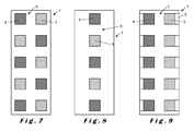
- Figure 7 for example shows that also the columns of the resulting array 7 are made up from alternating p-doped regions 4 and n-doped regions 5.
- the number of columns of the resulting array equals the number of arrays of doped regions 4, 5, such configuration is not critical for the disclosure as can for example be seen in figure 8 in which the resulting array 7 comprises a single column although comprising multiple arrays comprising either n-doped regions 5 or p-doped regions 4.
- the configuration of the resulting array 7 in other words does not depend on the number of arrays of comprising either n-doped regions 5 or p-doped regions 4 and can be determined by the person skilled in the art depending on the desired characteristics of the avalanche photodetector 1.
- Figure 10 shows a view in perspective of the embodiment shown in figure 7 .
- electric field lines between the p-doped regions 4 and the n-doped regions 5 are shown to illustrate the increase in PIN-junction avalanche photodiodes with respect to the prior art.
- figure 10 illustrates the configuration of the doped regions 4, 5 with respect to the waveguide 2 as for example shown in figures 2 and 3 .
- FIG 10 Also shown in figure 10 is the presence of electrodes 8 in and/or on the doped regions 4, 5 for interconnecting the avalanche photodetector 1 in an electrical circuit.
- the electrodes 8 have not been shown for clarity purposes in figures 4 - 8 .
- figure 10 shows that the electrodes 8 are applied on and/or in the doped regions 4, 5, this is not critical for the disclosure and the electrodes 8 can also be applied next to the doped regions 4, 5.
- This is for example shown in figure 9 where the electrodes 8 are applied next to the doped regions.
- the interference of the metal in the doped region where it is applied is lower as absorption of light in the doped regions is prevented, the capacitance of the diodes has been found to increase.
- the doped regions may be positioned substantially in a single plane, as is possible in the configurations shown in figures 2 - 10 , the doped regions can also be provided in different planes, forming a more three-dimensional configuration, as shown in the embodiment shown in different views in figures 11a - 11c and the alternative embodiment 11d.
- Figure 11a shows that for example on top of substrate 9 of, for example, Silicon dioxide, for example on its turn on top of a layer 10 of Silicon, an n-doped region 5 is provided. As shown, preferably several electrodes 8 are provided contacting the n-doped region 5.
- the intrinsic semiconducting material 3 for example Germanium
- an array of p-doped regions 4 is provided on the upper side of the intrinsic semiconducting material 3.
- the p-doped regions 4, for example p+ doped regions, are connected to electrodes 8.
- the space in between the different components is filled up with filling material 11, for example SiO 2 .
- the n-doped region 5 for example is made from Silicon material, the parts of the region 5 in close proximity with the electrodes 8 being highly doped (n++) whereas the parts of the doped region 5 further away from the electrodes 8 being less doped (n+).
- the doped region 5 could however also be homogenously highly or more lowly doped, as depends from the desired applications.
- the p-doped regions can be interchanged with the n-doped regions, as deemed appropriate in light of the desired applications of the photodetector element 1.
- Figure 11b shows the different p-doped regions 4 with respect to the underlying n-doped region 5 in more detail. Further, the relation between the input waveguide 2 and the intrinsic semiconducting material 3 is shown, allowing the optical waves to enter the intrinsic semiconducting material 3 where the optical waves can generate electron-hole pairs which can then subsequently be respectively accelerated towards the respective doped regions 4, 5.
- Figure 11c shows a top view of the avalanche photodetector element 1 according to figure 11a . It can be observed that the different p-doped regions are provided above and along the input waveguide 2. As shown in figure 11c , the p-doped regions 4 are collinear. However, as shown in figure 11d , such configuration is not critical and the different p-doped regions 4 can also be provided on, for example, different lines, for example parallel lines.
Landscapes
- Light Receiving Elements (AREA)
- Optical Couplings Of Light Guides (AREA)
- Optical Integrated Circuits (AREA)
Abstract
Description
- The current disclosure relates to an avalanche photodetector for converting an optical signal to an electrical signal according to the preamble of the first claim.
- The present disclosure also relates to use of such avalanche photodetector and a method for making such a avalanche photodetector.
- Infrared avalanche photodetectors are already known to the person skilled in the art. For example, the known avalanche photodetector element comprises an absorbing intrinsic semiconducting material with bandgap smaller than photon energy of the to-be-detected light wave, including Group IV semiconductors such as Germanium (Ge), Silicon-Germanium (SiGe), Germanium Tin (GeSn) or SiGeSn alloys, or alternatively, binary, ternary and quaternary III-V semiconductors, including but not limited to InP, InGaAs, InGaAsP and related materials. Light with infrared wavelengths can be coupled directly from free space into the absorbing semiconductor, or alternatively, can be guided and coupled into the absorbing semiconductor by means of an optically transparent input waveguide, which can be built from optically transparent semiconductors such as silicon. The absorbing semiconducting material comprises a p-doped region, an n-doped region, and an intrinsic region in between the doped regions. A schematic overview of such configuration is for example shown in
figure 1 . The p-doped , the n-doped and the intrinsic region are preferably implemented longitudinally along the propagation direction of the incoming light wave and extend with their longitudinal direction parallel to each other and parallel to the longitudinal direction of the absorbing material. The doped regions and the intrinsic semiconducting material thus form a PIN-junction photodiode wherein the input waveguide, if present, and the intrinsic semiconducting material are arranged with respect to each other such that optical waves, with typical infrared wavelengths greater than 1200nm, guided by the input waveguide are substantially coupled into the intrinsic semiconducting material to the so called PIN-junction, formed by the combination of a p-doped region, an n-doped region and the intrinsic semiconducting material in between them, forming a PIN photodiode. A reverse bias potential difference is applied between the p-doped region and the n-doped region, resulting in an electric field in the intrinsic region. At the intrinsic, absorbing region of the PIN-junction, the optical signal is converted to an electrical signal by optical excitation of electrons from the valence band to the conduction band under influence of the optical waves, essentially forming free electrons and free holes in the semiconducting material, which are subsequently collected at the n-doped region and p-doped region respectively, under the influence of the internal electric field. - For a sufficiently high electric field in the intrinsic region, the generated free electrons or the generated free holes, or both, can be multiplied by the mechanism known as impact ionization, essentially creating an avalanche of free electrons and/or holes. Such resulting multiplication gain essentially improves the responsiveness of the photodiode, potentially resulting in superior sensitivity of optical receivers built from such avalanche photodetectors. intrinsic semiconducting
- However, it has been found that for creating a sufficiently large multiplication gain of the free electrons and or holes, necessary for increased receiver sensitivity, a relatively strong electric field must be created in between the doped regions. Although the strength of the electric field can be increased by increasing the reverse bias potential difference over the doped regions, the increased potential difference requires for example more power leading to an increase in the power needed to use such avalanche photodetector element.
- Therefore, it is an aim of the current disclosure to increase the strength of the electric field without having to increase the bias potential difference.
- This is achieved according to an avalanche photodetector element according to the characterizing part of the first claim.
- Thereto, the semiconducting material comprises at least one array of p-doped regions or n-doped regions.
- It has been found that when the semiconducting material comprises at least one array of p-doped regions or n-doped regions on the same area as the avalanche photodetector element according to the state of the art, the dimensions of the different doped regions of the array are much smaller than the dimensions of the longitudinally shaped doped regions according to the state of the art. As the dimensions of the different doped regions are now smaller, the strength of the electric field will increase in the proximity of the doped regions without having to increase the reverse bias potential. Therefore, for example, the power required for operating the avalanche photodetector element does not need to be increased and can even be lowered with respect to the prior art avalanche photodetector element.
- Moreover, it has been found that by decreasing the dimensions of the doped regions, the volume of material surrounding the doped regions which is susceptible to creation of optically excited electrons is increased.
- Although in "Reinventing germanium avalanche photodetector for nanophotonic on-chip optical interconnects" by Solomon Assefa, Fengian Xia and Yurii A. Vlasov in Nature, Vol 464/4 March 2012 it is already discussed that strong non-uniform electric fields can be generated in avalanche photodetectors with relative small reverse bias potentials, the article relates to the use of avalanche photodetectors based on metal-semiconductor-metal Schottky detectors presenting, as described, high amplification noise characteristics and often a relatively large leakage current (dark current).
- According to preferred embodiments of the current disclosure, the doped regions of the array of p-doped regions or n-doped regions are delimited from each other by, more preferably undoped, intrinsic semiconducting material. The semiconductor material is provided to absorb the optical waves of the optical signal thereby creating a electron-hole pair which are than respectively accelerated to the respective doped regions under influence of the electric field.
- According to preferred embodiments of the current disclosure, the shape and position of the p-doped regions or n-doped regions of the PIN diode are implemented in such a way to locally increase the internal electric field generated by an external reverse bias applied to the diode electrodes. By implementing the n-doped and/or p-doped region of the PIN diode as an array of respectively n-doped and/or p-doped regions, it has been found that the electric field is enhanced compared to an implementation with only one p-type region and only one n-type region as shown in
figure 1 . In addition, alternating p-type and n-type regions further helps to improve the electrical field. Further, it is found that the electric field improvement is increased by reducing the size of the individual contacts and individual doped regions in the array, as well as by reducing the width of the intrinsic material in between the doped regions. - According to preferred embodiments of the current disclosure, the doped regions of the array of p-doped regions or n-doped regions are less, preferably substantially less, than 0.1 micron wide. Such dimensioned doped regions have been found to generate a sufficiently large electric field in their vicinity to allow avalanche electrons to be created without having to use relatively large voltages.
- According to preferred embodiments of the current disclosure, the at least one avalanche photodiode has a multiplication factor of more than one, preferably substantially greater than two, which has been found sufficient for the working of the avalanche photodetector element according to the disclosure.
- According to preferred embodiments of the current disclosure, the semiconducting material comprises at least an array of p-doped regions and an array of n-doped regions forming a resulting array of doped regions. It has been found that by employing both an array of p-doped regions and b-doped regions the strength of the electric field can be further increased as both the dimensions of the p-doped region as the n-doped regions are now reduced.
- According to preferred embodiments of the current disclosure, the rows and/or columns, preferably the rows and the columns, of the resulting array of doped regions are made up from p-doped regions and n-doped regions alternating each other. Such configuration of the different doped regions have been found to even further increase the volume of material which is susceptible to creation of optically excited electrons as some opposingly doped regions forming PIN-junction avalanche photodiodes are positioned adjacently along at least two sides of the doped regions and possible even along four sides of the doped regions when both the rows and the columns are provided with alternating p-doped regions and n-doped regions.
- According to preferred embodiments of the current disclosure, adjacent doped regions are delimited from each other with a delimiting distance of 0.05 micron - 0.5 micron, preferably 0.1 micron - 0.2 micron. Such distances have been found to provide further improved avalanche photodetectors.
- According to preferred embodiments of the current disclosure, the intrinsic semiconducting material comprises Germanium, Silicon-Germanium, Germanium-Tin,. It has been found that Germanium and Silicon-Germanium have good absorbing optical properties with optical waves having a wavelength of less than 1.6 micron. As such optical waves are often used for optical communication, for example over fiberglass communication lines, it has been found that such avalanche photodetectors can be used in optical communication applications. Germanium-Tin has been found to present improved absorption for wavelengths above 1.6micron.
- According to preferred embodiments of the current disclosure, the input waveguide comprises Silicon, preferably substantially Silicon, most preferable is made from Silicon, as silicon has does not substantially absorb optical waves having a wavelength in the range 1.2 - 3 micron, preferably 1.3 micron - 1.6 micron which are often used in optical communications.
- According to preferred embodiments of the current disclosure, the doped regions are provided with electrodes for interconnecting the avalanche photodetector in an electrical circuit.
- The disclosure also relates to an electrical circuit comprising the avalanche photodetector according to the disclosure wherein in use a reverse bias potential difference is applied over the p-doped region and the n-doped region forming the PIN-junction avalanche photodiode. The electrical circuit can for example be incorporated on a chip.
- The disclosure also relates to a method for making the avalanche photodetector according to the disclosure.
- The doped regions can for example be made by ion-implantation, preferably followed by annealing or selective epitaxy.
- The disclosure also relates to the use of the avalanche photodetector according to the disclosure for converting an optical signal to an electrical signal. Such use is for example especially preferred in optical communication applications.
- According to preferred embodiments of the current disclosure, the optic waves have a wavelength in the range 1.2-3 micron, preferably 1.3 micron - 1.6 micron as such wavelengths are often used in optical communications applications, as discussed above.
- According to preferred embodiments of the current disclosure, a reverse bias potential difference is applied over the p-doped region and the n-doped region forming the PIN-junction avalanche photodiode.
- According to preferred embodiments of the current disclosure, the reverse bias potential difference is about 1V - 10V, preferably 2V - 4V as such reverse bias potential differences have been found to be quite available in for example chip applications whereas nevertheless being sufficiently high to create avalanche electrons. Good results are expected at for example 2V.
- According to preferred embodiments of the current disclosure, the reverse bias is applied to the preferred electrodes discussed above.
- The disclosure will be further elucidated by means of the following description and the appended figures.
-
Figure 1 shows a top view of an avalanche photodetector according to the prior art. -
Figure 2 shows a cross section of a side view of a avalanche photodetector element according to the present disclosure. -
Figure 3 shows a cross section of a frontal view of the avalanche photodetector element according tofigure 2 . -
Figure 4 shows a top view of a first embodiment of part of the avalanche photodetector element according to the disclosure. -
Figure 5 shows a top view of an alternative embodiment offigure 4 . -
Figure 6 shows a top view of an alternative embodiment offigure 4 . -
Figure 7 shows a top view of an alternative embodiment offigure 4 . -
Figure 8 shows a top view of an alternative embodiment offigure 4 . -
Figure 9 shows a top view of an alternative embodiment offigure 4 . -
Figure 10 shows a view in perspective of the embodiment shown infigure 7 . -
Figure 11a shows a cross section of a frontal view of the avalanche photodetector element according to a different embodiment of the present disclosure. -
Figure 11b shows a cross section of a side view of the avalanche photodetector element according tofigure 11a . -
Figure 11c shows a top view of the avalanche photodetector element according tofigure 11a . -
Figure 11d shows a top view of a different embodiment of the avalanche photodetector element according tofigure 11a . - In the following detailed description, numerous specific details are set forth in order to provide a thorough understanding of the disclosure and how it may be practiced in particular embodiments. However, it will be understood that the present disclosure may be practiced without these specific details. In other instances, well-known methods, procedures and techniques have not been described in detail, so as not to obscure the present disclosure. While the present disclosure will be described with respect to particular embodiments and with reference to certain drawings, the disclosure is not limited hereto. The drawings included and described herein are schematic and are not limiting the scope of the disclosure. It is also noted that in the drawings, the size of some elements may be exaggerated and, therefore, not drawn to scale for illustrative purposes.
- The present disclosure will be described with respect to particular embodiments and with reference to certain drawings but the disclosure is not limited thereto but only by the claims. The drawings described are only schematic and are non-limiting. In the drawings, the size of some of the elements may be exaggerated and not drawn on scale for illustrative purposes. The dimensions and the relative dimensions do not necessarily correspond to actual reductions to practice of the disclosure.
- Furthermore, the terms first, second, third and the like in the description and in the claims, are used for distinguishing between similar elements and not necessarily for describing a sequential or chronological order. The terms are interchangeable under appropriate circumstances and the embodiments of the disclosure can operate in other sequences than described or illustrated herein.
- Moreover, the terms top, bottom, over, under and the like in the description and the claims are used for descriptive purposes and not necessarily for describing relative positions. It is to be understood that the terms so used are interchangeable under appropriate circumstances and that the embodiments of the disclosure described herein are capable of operation in other orientations than described or illustrated herein.
- The term "comprising", used in the claims, should not be interpreted as being restricted to the means listed thereafter; it does not exclude other elements or steps. It needs to be interpreted as specifying the presence of the stated features, integers, steps or components as referred to, but does not preclude the presence or addition of one or more other features, integers, steps or components, or groups thereof. Thus, the scope of the expression "a device comprising means A and B" should not be limited to devices consisting only of components A and B.
-
Figure 2 shows a cross section of a side view of aavalanche photodetector element 1 for converting an optical signal to an electrical signal according to the present disclosure. - The
avalanche photodetector element 1 comprises aninput waveguide 2 and an intrinsic, absorbingsemiconducting material 3. Thesemiconducting material 3 comprises at least one p-dopedregion 4 and at least one n-dopedregion 5. Although thedoped regions figure 2 , thedoped regions figure 3 . Thedoped regions semiconducting material 3 form at least one PIN-junction avalanche photodiode 6. - The
input waveguide 2 and the intrinsicsemiconducting material 3 are arranged with respect to each other such that optical waves conducted by theinput waveguide 2 are substantially conducted into the intrinsicsemiconducting material 3 to the PIN-junction avalanche photodiode 6. In the PIN-junction avalanche photodiode 6 the optical signal is converted to an electrical signal. - The precise configuration, such as for example dimensions, shape, etc., of the
input waveguide 2 and the intrinsicsemiconducting material 3, keeping their above-described functionality in mind, is not essential for the disclosure and can be further determined by the person skilled in the art depending on for example the characteristics, such as for example wavelength, intensity, etc., of the optical waves used, the intrinsicsemiconducting material 3, the material of thewaveguide 2, etc. - Although not shown in the figures, the disclosure also relates to an electrical circuit comprising the
avalanche photodetector 1 according to the disclosure. In such electrical circuit, in use a reverse bias potential difference is applied over the p-dopedregion 4 and the n-dopedregion 5 forming the PIN-junction avalanche photodiode 6. - Although not shown in
figures 2 and 3 , thesemiconducting material 3 comprises at least one array of p-dopedregions 4 or n-dopedregion 5. Different possibilities of arrays of the dopedregions figures 4 - 10 . -
Figure 4 for example shows a top view of a first embodiment of part of theavalanche photodetector element 1 according to the disclosure. - According to
figure 4 , theavalanche photodetector element 1 comprises an array of n-dopedregions 5. However, this is not critical for the disclosure and as shown infigure 5 , theavalanche photodetector element 1 can also comprise an array of p-dopedregions 5. - The
array semiconducting material 3 along that propagation direction. In general the length of the intrinsicsemiconducting material 3 along that propagation direction is in the range 5 - 100 micron. - As can be seen in
figures 4 and 5 , thedoped regions regions 4 or n-dopedregions 5 are delimited from each other by undoped intrinsicsemiconducting material 3. - In
figures 4 and 5 the array ofdoped regions - In
figures 4 and 5 the respective p-doped region and n-doped region opposing the respective array of n-dopedregions 5 or p-dopedregions 4 is in the form of a single uninterrupted doped region.Figure 6 shows a further preferred embodiment wherein the single uninterrupted doped region is also replaced by an array of doped regions. The arrays of n-doped regions and p-dopedregions doped regions 7. - According to
figure 6 , the resulting array ofdoped regions 7 comprises two arrays ofdoped regions region 5 and one p-dopedregion 4. This is however not critical for the disclosure and the resulting array ofdoped regions 7 can also comprise three, four, five, six, seven, eight, nine, ten, eleven, twelve, thirteen, fourteen, fifteen, twenty, twenty-five, thirty, thirty-five, forty, etc. arrays ofdoped regions regions 4 and the number of n-doped regions also do not need to be the same. - Although the rows of the resulting
array 7 shown infigure 6 is made up from alternating p-dopedregions 4 and n-dopedregions 5, such configuration is not critical for the disclosure.Figure 7 for example shows that also the columns of the resultingarray 7 are made up from alternating p-dopedregions 4 and n-dopedregions 5. Although not shown in the figures it is also possible that only the columns of the resultingarray 7 are made up from alternating p-dopedregions 4 and n-dopedregions 5. - Although in
figures 6 and7 , the number of columns of the resulting array equals the number of arrays ofdoped regions figure 8 in which the resultingarray 7 comprises a single column although comprising multiple arrays comprising either n-dopedregions 5 or p-dopedregions 4. The configuration of the resultingarray 7 in other words does not depend on the number of arrays of comprising either n-dopedregions 5 or p-dopedregions 4 and can be determined by the person skilled in the art depending on the desired characteristics of theavalanche photodetector 1. -
Figure 10 shows a view in perspective of the embodiment shown infigure 7 . In addition electric field lines between the p-dopedregions 4 and the n-dopedregions 5 are shown to illustrate the increase in PIN-junction avalanche photodiodes with respect to the prior art. Furthermore,figure 10 illustrates the configuration of the dopedregions waveguide 2 as for example shown infigures 2 and 3 . - Also shown in
figure 10 is the presence ofelectrodes 8 in and/or on thedoped regions avalanche photodetector 1 in an electrical circuit. Theelectrodes 8 have not been shown for clarity purposes infigures 4 - 8 . Althoughfigure 10 shows that theelectrodes 8 are applied on and/or in the dopedregions electrodes 8 can also be applied next to the dopedregions figure 9 where theelectrodes 8 are applied next to the doped regions. Although in such configuration the interference of the metal in the doped region where it is applied is lower as absorption of light in the doped regions is prevented, the capacitance of the diodes has been found to increase. - Although the doped regions may be positioned substantially in a single plane, as is possible in the configurations shown in
figures 2 - 10 , the doped regions can also be provided in different planes, forming a more three-dimensional configuration, as shown in the embodiment shown in different views infigures 11a - 11c and the alternative embodiment 11d. -
Figure 11a shows that for example on top ofsubstrate 9 of, for example, Silicon dioxide, for example on its turn on top of alayer 10 of Silicon, an n-dopedregion 5 is provided. As shown, preferablyseveral electrodes 8 are provided contacting the n-dopedregion 5. - On top of the n-doped
region 5 the intrinsicsemiconducting material 3, for example Germanium, is provided. On the upper side of the intrinsicsemiconducting material 3, an array of p-dopedregions 4 is provided. In their turn, the p-dopedregions 4, for example p+ doped regions, are connected toelectrodes 8. The space in between the different components is filled up with fillingmaterial 11, for example SiO2. - The n-doped
region 5 for example is made from Silicon material, the parts of theregion 5 in close proximity with theelectrodes 8 being highly doped (n++) whereas the parts of the dopedregion 5 further away from theelectrodes 8 being less doped (n+). The dopedregion 5 could however also be homogenously highly or more lowly doped, as depends from the desired applications. - Of course the p-doped regions can be interchanged with the n-doped regions, as deemed appropriate in light of the desired applications of the
photodetector element 1. -
Figure 11b shows the different p-dopedregions 4 with respect to the underlying n-dopedregion 5 in more detail. Further, the relation between theinput waveguide 2 and the intrinsicsemiconducting material 3 is shown, allowing the optical waves to enter the intrinsicsemiconducting material 3 where the optical waves can generate electron-hole pairs which can then subsequently be respectively accelerated towards the respectivedoped regions Figure 11c shows a top view of theavalanche photodetector element 1 according tofigure 11a . It can be observed that the different p-doped regions are provided above and along theinput waveguide 2. As shown infigure 11c , the p-dopedregions 4 are collinear. However, as shown infigure 11d , such configuration is not critical and the different p-dopedregions 4 can also be provided on, for example, different lines, for example parallel lines.
Claims (15)
- Avalanche photodetector element (1) for converting an optical signal to an electrical signal, comprising an input waveguide (2) and an intrinsic semiconducting material (3), the semiconducting material (3) comprising at least one p-doped region (4) and at least one n-doped region (5), the doped regions (4, 5) and the intrinsic semiconducting material (3) forming at least one PIN-junction avalanche photodiode (6), the input waveguide (2) and the intrinsic semiconducting material (3) being arranged with respect to each other such that optical waves conducted by the input waveguide (2) are substantially conducted into the intrinsic semiconducting material (3) to the PIN-junction avalanche photodiode (6) converting the optical signal to an electrical signal, characterized in that the semiconducting material (3) comprises at least one array of p-doped regions (4) or n-doped regions (5).
- Avalanche photodetector (1) according to claim 1, wherein the doped regions (4, 5) of the array of p-doped regions (4) or n-doped regions (5) are delimited from each other by undoped intrinsic semiconducting material (3).
- Avalanche photodetector (1) according to claim 1 or 2, wherein the doped regions (4, 5) of the array of p-doped regions (4) or n-doped regions (5) are substantially less than 0.1 micron wide.
- Avalanche photodetector (1) according to any one of claims 1 - 3, wherein the at least one avalanche photodiode (6) has a multiplication factor of more than one, preferably substantially greater than two.
- Avalanche photodetector (1) according to any one of claims 1 - 4, wherein the semiconducting material (3) comprises at least an array of p-doped regions (4) and an array of n-doped regions (5) forming a resulting array of doped regions (7).
- Avalanche photodetector (1) according to claim 5, wherein the rows and/or columns of the resulting array of doped regions (7) are made up from p-doped regions (4) and n-doped regions (5) alternating each other.
- Avalanche photodetector (1) according to any one of claims 1 - 6, wherein adjacent doped regions (4, 5) are delimited from each other with a delimiting distance of 0.05 micron - 0.5 micron, preferably 0.1 micron - 0.2 micron.
- Avalanche photodetector (1) according to any one of claims 1 - 7, wherein the doped regions (4, 5) are provided with electrodes (8) for interconnecting the avalanche photodetector (1) in an electrical circuit.
- Electrical circuit comprising the avalanche photodetector (1) according to any one of claims 1 - 8, wherein in use a reverse bias potential difference is applied over the p-doped region (4) and the n-doped region (5) forming the PIN-junction avalanche photodiode (6).
- Method of making the avalanche photodetector (1) according to any one of claims 1 - 8 or the electrical circuit according to claim 11.
- Use of the avalanche photodetector (1) according to any one of claims 1 - 8 for converting an optical signal to an electrical signal.
- Use according to claim 11, wherein the optic waves have a wavelength of 1.3 micron - 1.6 micron, preferably 1.53 micron - 1.56 micron.
- Use according to claim 11 or 12, wherein a reverse bias potential difference is applied over the p-doped region (4) and the n-doped region (5) forming the PIN-junction avalanche photodiode (6).
- Use according to claim 13, wherein the reverse bias potential difference is about 1V - 10V, preferably 2V - 4V.
- Use according to claim 13 or 14 at least in combination with claim 8, wherein the reverse bias is applied to the electrodes (8).
Priority Applications (3)
| Application Number | Priority Date | Filing Date | Title |
|---|---|---|---|
| EP12193767.6A EP2736084B1 (en) | 2012-11-22 | 2012-11-22 | Avalanche photodetector element with increased electric field strength |
| JP2013241541A JP6341651B2 (en) | 2012-11-22 | 2013-11-22 | Avalanche photodetector elements that convert optical signals into electrical signals, electrical circuits using the same, and use of avalanche photodetectors |
| US14/087,983 US9159860B2 (en) | 2012-11-22 | 2013-11-22 | Avalanche photodetector element |
Applications Claiming Priority (1)
| Application Number | Priority Date | Filing Date | Title |
|---|---|---|---|
| EP12193767.6A EP2736084B1 (en) | 2012-11-22 | 2012-11-22 | Avalanche photodetector element with increased electric field strength |
Publications (2)
| Publication Number | Publication Date |
|---|---|
| EP2736084A1 true EP2736084A1 (en) | 2014-05-28 |
| EP2736084B1 EP2736084B1 (en) | 2018-09-19 |
Family
ID=47221974
Family Applications (1)
| Application Number | Title | Priority Date | Filing Date |
|---|---|---|---|
| EP12193767.6A Active EP2736084B1 (en) | 2012-11-22 | 2012-11-22 | Avalanche photodetector element with increased electric field strength |
Country Status (3)
| Country | Link |
|---|---|
| US (1) | US9159860B2 (en) |
| EP (1) | EP2736084B1 (en) |
| JP (1) | JP6341651B2 (en) |
Cited By (3)
| Publication number | Priority date | Publication date | Assignee | Title |
|---|---|---|---|---|
| EP3038167A1 (en) * | 2014-12-22 | 2016-06-29 | IMEC vzw | Integrated avalanche germanium photodetector |
| CN110494800A (en) * | 2017-03-24 | 2019-11-22 | 洛克利光子有限公司 | Optical modulator |
| US20230085007A1 (en) * | 2021-09-16 | 2023-03-16 | Fujitsu Optical Components Limited | Photodetector and photonic integrated device |
Families Citing this family (17)
| Publication number | Priority date | Publication date | Assignee | Title |
|---|---|---|---|---|
| US10431707B2 (en) | 2015-04-30 | 2019-10-01 | Hewlett Packard Enterprise Development Lp | Monolithically integrated photodetector and receiver |
| SG11201801176SA (en) * | 2015-08-28 | 2018-03-28 | Nippon Telegraph & Telephone | Photodetector |
| JP6879919B2 (en) * | 2015-09-17 | 2021-06-02 | ソニーセミコンダクタソリューションズ株式会社 | Manufacturing method of solid-state image sensor, electronic device, and solid-state image sensor |
| US10418407B2 (en) | 2015-11-06 | 2019-09-17 | Artilux, Inc. | High-speed light sensing apparatus III |
| US10886309B2 (en) | 2015-11-06 | 2021-01-05 | Artilux, Inc. | High-speed light sensing apparatus II |
| US10254389B2 (en) | 2015-11-06 | 2019-04-09 | Artilux Corporation | High-speed light sensing apparatus |
| JP7024976B2 (en) | 2016-07-26 | 2022-02-24 | コニカミノルタ株式会社 | Light receiving element and near infrared photodetector |
| US11049851B2 (en) * | 2017-06-08 | 2021-06-29 | Luxtera Llc | Method and system for selectively illuminated integrated photodetectors with configured launching and adaptive junction profile for bandwidth improvement |
| WO2019137620A1 (en) * | 2018-01-12 | 2019-07-18 | Iris Industries Sa | Short-wave infrared detector and its integration with cmos compatible substrates |
| JP6975341B2 (en) * | 2018-02-23 | 2021-12-01 | アーティラックス・インコーポレイテッド | Photodetector and its light detection method |
| US11482553B2 (en) | 2018-02-23 | 2022-10-25 | Artilux, Inc. | Photo-detecting apparatus with subpixels |
| US11105928B2 (en) | 2018-02-23 | 2021-08-31 | Artilux, Inc. | Light-sensing apparatus and light-sensing method thereof |
| CN114335030A (en) | 2018-04-08 | 2022-04-12 | 奥特逻科公司 | Optical detection device |
| GB2576491A (en) * | 2018-07-17 | 2020-02-26 | Cambridge Entpr Ltd | A photodetector |
| US11367803B2 (en) * | 2020-04-01 | 2022-06-21 | Taiwan Semiconductor Manufacturing Company Ltd. | Light detecting device, optical device and method of manufacturing the same |
| CN112289883B (en) * | 2020-10-30 | 2023-03-28 | 华中科技大学 | Three-dimensional semiconductor avalanche photoelectric detection chip and preparation method thereof |
| JP7639592B2 (en) * | 2021-07-19 | 2025-03-05 | 富士通オプティカルコンポーネンツ株式会社 | Semiconductor photoreceiver, receiver and optical integrated device |
Citations (2)
| Publication number | Priority date | Publication date | Assignee | Title |
|---|---|---|---|---|
| EP1833095A1 (en) * | 2006-03-06 | 2007-09-12 | Austriamicrosystems AG | Photo diode having reduced dark current |
| US20100282948A1 (en) * | 2008-10-22 | 2010-11-11 | Panasonic Corporation | Optical semiconductor device |
Family Cites Families (14)
| Publication number | Priority date | Publication date | Assignee | Title |
|---|---|---|---|---|
| JPS61271875A (en) * | 1985-05-27 | 1986-12-02 | Mitsubishi Electric Corp | Semiconductor light receiving element |
| JPS62130521A (en) * | 1985-12-02 | 1987-06-12 | Nippon Telegr & Teleph Corp <Ntt> | Semiconductor device and manufacture of the same |
| JPH03203273A (en) * | 1989-12-28 | 1991-09-04 | Hamamatsu Photonics Kk | Pin photodiode |
| JPH06252435A (en) * | 1993-02-23 | 1994-09-09 | Toshiba Corp | Photodetective device |
| JPH0832105A (en) * | 1994-07-21 | 1996-02-02 | Hitachi Ltd | Optical semiconductor device |
| JP2701754B2 (en) * | 1994-10-03 | 1998-01-21 | 日本電気株式会社 | Method for manufacturing silicon light receiving element |
| JP3610910B2 (en) * | 2001-01-22 | 2005-01-19 | 日本電気株式会社 | Semiconductor photo detector |
| US9813152B2 (en) * | 2004-01-14 | 2017-11-07 | Luxtera, Inc. | Method and system for optoelectronics transceivers integrated on a CMOS chip |
| US7397101B1 (en) * | 2004-07-08 | 2008-07-08 | Luxtera, Inc. | Germanium silicon heterostructure photodetectors |
| EP1670066A1 (en) * | 2004-12-08 | 2006-06-14 | St Microelectronics S.A. | Fabrication method for an integrated circuit including a buried mirror and such circuit |
| US7209623B2 (en) * | 2005-05-03 | 2007-04-24 | Intel Corporation | Semiconductor waveguide-based avalanche photodetector with separate absorption and multiplication regions |
| US7613369B2 (en) | 2006-04-13 | 2009-11-03 | Luxtera, Inc. | Design of CMOS integrated germanium photodiodes |
| JP4924617B2 (en) * | 2009-01-05 | 2012-04-25 | ソニー株式会社 | Solid-state image sensor, camera |
| US8232516B2 (en) | 2009-07-31 | 2012-07-31 | International Business Machines Corporation | Avalanche impact ionization amplification devices |
-
2012
- 2012-11-22 EP EP12193767.6A patent/EP2736084B1/en active Active
-
2013
- 2013-11-22 JP JP2013241541A patent/JP6341651B2/en active Active
- 2013-11-22 US US14/087,983 patent/US9159860B2/en active Active
Patent Citations (2)
| Publication number | Priority date | Publication date | Assignee | Title |
|---|---|---|---|---|
| EP1833095A1 (en) * | 2006-03-06 | 2007-09-12 | Austriamicrosystems AG | Photo diode having reduced dark current |
| US20100282948A1 (en) * | 2008-10-22 | 2010-11-11 | Panasonic Corporation | Optical semiconductor device |
Non-Patent Citations (5)
| Title |
|---|
| ASSEFA S ET AL: "CMOS-integrated 40GHz germanium waveguide photodetector for on-chip optical interconnects", OPTICAL FIBER COMMUNICATION - INCUDES POST DEADLINE PAPERS, 2009. OFC 2009. CONFERENCE ON, IEEE, PISCATAWAY, NJ, USA, 22 March 2009 (2009-03-22), pages 1 - 3, XP031467714, ISBN: 978-1-4244-2606-5 * |
| GUOLIANG LI ET AL: "Improving CMOS-compatible Germanium photodetectors", OPTICS EXPRESS, vol. 20, no. 24, 7 November 2012 (2012-11-07), pages 26345 - 26350, XP055060563, ISSN: 1094-4087, DOI: 10.1364/OE.20.026345 * |
| SOLOMON ASSEFA ET AL: "CMOS-Integrated Optical Receivers for On-Chip Interconnects", IEEE JOURNAL OF SELECTED TOPICS IN QUANTUM ELECTRONICS, IEEE SERVICE CENTER, PISCATAWAY, NJ, US, vol. 16, no. 5, 1 September 2010 (2010-09-01), pages 1376 - 1385, XP011310935, ISSN: 1077-260X * |
| SOLOMON ASSEFA ET AL: "Reinventing germanium avalanche photodetector for nanophotonic on-chip optical interconnects", NATURE, vol. 464, no. 7285, 4 March 2010 (2010-03-04), pages 80 - 84, XP055061103, ISSN: 0028-0836, DOI: 10.1038/nature08813 * |
| SOLOMON ASSEFA; FENGIAN XIA; YURII A. VLASOV: "Reinventing germanium avalanche photodetector for nanophotonic on-chip optical interconnects", NATURE, vol. 464, 4 March 2012 (2012-03-04) |
Cited By (5)
| Publication number | Priority date | Publication date | Assignee | Title |
|---|---|---|---|---|
| EP3038167A1 (en) * | 2014-12-22 | 2016-06-29 | IMEC vzw | Integrated avalanche germanium photodetector |
| US9472705B2 (en) | 2014-12-22 | 2016-10-18 | Imec Vzw | Integrated avalanche germanium photodetector |
| CN110494800A (en) * | 2017-03-24 | 2019-11-22 | 洛克利光子有限公司 | Optical modulator |
| US20230085007A1 (en) * | 2021-09-16 | 2023-03-16 | Fujitsu Optical Components Limited | Photodetector and photonic integrated device |
| US12560761B2 (en) * | 2021-09-16 | 2026-02-24 | Fujitsu Optical Components Limited | Photodetector and photonic integrated device |
Also Published As
| Publication number | Publication date |
|---|---|
| US20140138787A1 (en) | 2014-05-22 |
| US9159860B2 (en) | 2015-10-13 |
| EP2736084B1 (en) | 2018-09-19 |
| JP6341651B2 (en) | 2018-06-13 |
| JP2014107562A (en) | 2014-06-09 |
Similar Documents
| Publication | Publication Date | Title |
|---|---|---|
| EP2736084B1 (en) | Avalanche photodetector element with increased electric field strength | |
| US6963089B2 (en) | Avalanche photo-detector with high saturation power and high gain-bandwidth product | |
| CN108541343B (en) | ESD protection structure | |
| US9219184B2 (en) | Avalanche photodiodes with defect-assisted silicon absorption regions | |
| EP2808908B1 (en) | High-speed photodetector | |
| US10612971B2 (en) | Plasmonic avalanche photodetection | |
| CN118538821A (en) | Optical device and imaging system | |
| US20190019903A1 (en) | SILICON WAVEGUIDE INTEGRATED WITH SILICON-GERMANIUM (Si-Ge) AVALANCHE PHOTODIODE DETECTOR | |
| CN105390556A (en) | Absorption region structure for unitraveling carrier photodiode | |
| CN108538865B (en) | Silicon-based three-photoelectric detector | |
| CN115295646A (en) | A high-performance photodetector chip epitaxial wafer | |
| JPS59124776A (en) | Semiconductor photoelectric energy conversion device | |
| Khan et al. | Detailed analysis on the spectral response of InP/InGaAs HPTs for optoelectronic applications | |
| JP6362142B2 (en) | Germanium receiver | |
| Lee et al. | Performance Comparison of Two Types of Silicon Avalanche Photodetectors Based on N-well/P-substrate and P^+/N-well Junctions Fabricated With Standard CMOS Technology | |
| CN211957666U (en) | Photoelectric avalanche diode applied to sensing front end of high-sensitivity optical coupling isolation chip | |
| JP3365329B2 (en) | Light-to-voltage conversion type semiconductor light receiving device, optical signal processing device, and optical integrated device | |
| JP6206834B2 (en) | Quantum dot type high-speed photodiode | |
| TW202127639A (en) | Optical apparatus, optical system, time-of-flight system and three-dimensional imaging system | |
| Emami-Nejad et al. | Simulation and evaluation of PIN photodetectors based on material and thickness of intrinsic layer | |
| US20250359358A1 (en) | Photonic Surface-Topography in Single Photon Avalanche Diodes | |
| JP3610910B2 (en) | Semiconductor photo detector | |
| Wang et al. | Investigation of high-speed Si photodetectors in standard CMOS technology | |
| Mil’shtein et al. | Design of Solar Blind Photodetectors for Communication with Red Signal (λ= 650nm) in Space. Part I | |
| Gong et al. | A Multi-Band Si-InGaAs/InP Avalanche Photodetector |
Legal Events
| Date | Code | Title | Description |
|---|---|---|---|
| PUAI | Public reference made under article 153(3) epc to a published international application that has entered the european phase |
Free format text: ORIGINAL CODE: 0009012 |
|
| 17P | Request for examination filed |
Effective date: 20121122 |
|
| AK | Designated contracting states |
Kind code of ref document: A1 Designated state(s): AL AT BE BG CH CY CZ DE DK EE ES FI FR GB GR HR HU IE IS IT LI LT LU LV MC MK MT NL NO PL PT RO RS SE SI SK SM TR |
|
| AX | Request for extension of the european patent |
Extension state: BA ME |
|
| R17P | Request for examination filed (corrected) |
Effective date: 20140930 |
|
| RBV | Designated contracting states (corrected) |
Designated state(s): AL AT BE BG CH CY CZ DE DK EE ES FI FR GB GR HR HU IE IS IT LI LT LU LV MC MK MT NL NO PL PT RO RS SE SI SK SM TR |
|
| RAP1 | Party data changed (applicant data changed or rights of an application transferred) |
Owner name: IMEC VZW |
|
| 17Q | First examination report despatched |
Effective date: 20180104 |
|
| GRAP | Despatch of communication of intention to grant a patent |
Free format text: ORIGINAL CODE: EPIDOSNIGR1 |
|
| INTG | Intention to grant announced |
Effective date: 20180604 |
|
| GRAS | Grant fee paid |
Free format text: ORIGINAL CODE: EPIDOSNIGR3 |
|
| GRAA | (expected) grant |
Free format text: ORIGINAL CODE: 0009210 |
|
| AK | Designated contracting states |
Kind code of ref document: B1 Designated state(s): AL AT BE BG CH CY CZ DE DK EE ES FI FR GB GR HR HU IE IS IT LI LT LU LV MC MK MT NL NO PL PT RO RS SE SI SK SM TR |
|
| REG | Reference to a national code |
Ref country code: GB Ref legal event code: FG4D |
|
| REG | Reference to a national code |
Ref country code: CH Ref legal event code: EP |
|
| REG | Reference to a national code |
Ref country code: AT Ref legal event code: REF Ref document number: 1044244 Country of ref document: AT Kind code of ref document: T Effective date: 20181015 |
|
| REG | Reference to a national code |
Ref country code: IE Ref legal event code: FG4D |
|
| REG | Reference to a national code |
Ref country code: DE Ref legal event code: R096 Ref document number: 602012051214 Country of ref document: DE |
|
| REG | Reference to a national code |
Ref country code: NL Ref legal event code: MP Effective date: 20180919 |
|
| PG25 | Lapsed in a contracting state [announced via postgrant information from national office to epo] |
Ref country code: GR Free format text: LAPSE BECAUSE OF FAILURE TO SUBMIT A TRANSLATION OF THE DESCRIPTION OR TO PAY THE FEE WITHIN THE PRESCRIBED TIME-LIMIT Effective date: 20181220 Ref country code: BG Free format text: LAPSE BECAUSE OF FAILURE TO SUBMIT A TRANSLATION OF THE DESCRIPTION OR TO PAY THE FEE WITHIN THE PRESCRIBED TIME-LIMIT Effective date: 20181219 Ref country code: RS Free format text: LAPSE BECAUSE OF FAILURE TO SUBMIT A TRANSLATION OF THE DESCRIPTION OR TO PAY THE FEE WITHIN THE PRESCRIBED TIME-LIMIT Effective date: 20180919 Ref country code: LT Free format text: LAPSE BECAUSE OF FAILURE TO SUBMIT A TRANSLATION OF THE DESCRIPTION OR TO PAY THE FEE WITHIN THE PRESCRIBED TIME-LIMIT Effective date: 20180919 Ref country code: NO Free format text: LAPSE BECAUSE OF FAILURE TO SUBMIT A TRANSLATION OF THE DESCRIPTION OR TO PAY THE FEE WITHIN THE PRESCRIBED TIME-LIMIT Effective date: 20181219 Ref country code: FI Free format text: LAPSE BECAUSE OF FAILURE TO SUBMIT A TRANSLATION OF THE DESCRIPTION OR TO PAY THE FEE WITHIN THE PRESCRIBED TIME-LIMIT Effective date: 20180919 Ref country code: SE Free format text: LAPSE BECAUSE OF FAILURE TO SUBMIT A TRANSLATION OF THE DESCRIPTION OR TO PAY THE FEE WITHIN THE PRESCRIBED TIME-LIMIT Effective date: 20180919 |
|
| REG | Reference to a national code |
Ref country code: LT Ref legal event code: MG4D |
|
| PG25 | Lapsed in a contracting state [announced via postgrant information from national office to epo] |
Ref country code: LV Free format text: LAPSE BECAUSE OF FAILURE TO SUBMIT A TRANSLATION OF THE DESCRIPTION OR TO PAY THE FEE WITHIN THE PRESCRIBED TIME-LIMIT Effective date: 20180919 Ref country code: AL Free format text: LAPSE BECAUSE OF FAILURE TO SUBMIT A TRANSLATION OF THE DESCRIPTION OR TO PAY THE FEE WITHIN THE PRESCRIBED TIME-LIMIT Effective date: 20180919 Ref country code: HR Free format text: LAPSE BECAUSE OF FAILURE TO SUBMIT A TRANSLATION OF THE DESCRIPTION OR TO PAY THE FEE WITHIN THE PRESCRIBED TIME-LIMIT Effective date: 20180919 |
|
| REG | Reference to a national code |
Ref country code: AT Ref legal event code: MK05 Ref document number: 1044244 Country of ref document: AT Kind code of ref document: T Effective date: 20180919 |
|
| PG25 | Lapsed in a contracting state [announced via postgrant information from national office to epo] |
Ref country code: AT Free format text: LAPSE BECAUSE OF FAILURE TO SUBMIT A TRANSLATION OF THE DESCRIPTION OR TO PAY THE FEE WITHIN THE PRESCRIBED TIME-LIMIT Effective date: 20180919 Ref country code: IS Free format text: LAPSE BECAUSE OF FAILURE TO SUBMIT A TRANSLATION OF THE DESCRIPTION OR TO PAY THE FEE WITHIN THE PRESCRIBED TIME-LIMIT Effective date: 20190119 Ref country code: IT Free format text: LAPSE BECAUSE OF FAILURE TO SUBMIT A TRANSLATION OF THE DESCRIPTION OR TO PAY THE FEE WITHIN THE PRESCRIBED TIME-LIMIT Effective date: 20180919 Ref country code: EE Free format text: LAPSE BECAUSE OF FAILURE TO SUBMIT A TRANSLATION OF THE DESCRIPTION OR TO PAY THE FEE WITHIN THE PRESCRIBED TIME-LIMIT Effective date: 20180919 Ref country code: PL Free format text: LAPSE BECAUSE OF FAILURE TO SUBMIT A TRANSLATION OF THE DESCRIPTION OR TO PAY THE FEE WITHIN THE PRESCRIBED TIME-LIMIT Effective date: 20180919 Ref country code: NL Free format text: LAPSE BECAUSE OF FAILURE TO SUBMIT A TRANSLATION OF THE DESCRIPTION OR TO PAY THE FEE WITHIN THE PRESCRIBED TIME-LIMIT Effective date: 20180919 Ref country code: ES Free format text: LAPSE BECAUSE OF FAILURE TO SUBMIT A TRANSLATION OF THE DESCRIPTION OR TO PAY THE FEE WITHIN THE PRESCRIBED TIME-LIMIT Effective date: 20180919 Ref country code: RO Free format text: LAPSE BECAUSE OF FAILURE TO SUBMIT A TRANSLATION OF THE DESCRIPTION OR TO PAY THE FEE WITHIN THE PRESCRIBED TIME-LIMIT Effective date: 20180919 Ref country code: CZ Free format text: LAPSE BECAUSE OF FAILURE TO SUBMIT A TRANSLATION OF THE DESCRIPTION OR TO PAY THE FEE WITHIN THE PRESCRIBED TIME-LIMIT Effective date: 20180919 |
|
| PG25 | Lapsed in a contracting state [announced via postgrant information from national office to epo] |
Ref country code: PT Free format text: LAPSE BECAUSE OF FAILURE TO SUBMIT A TRANSLATION OF THE DESCRIPTION OR TO PAY THE FEE WITHIN THE PRESCRIBED TIME-LIMIT Effective date: 20190119 Ref country code: SM Free format text: LAPSE BECAUSE OF FAILURE TO SUBMIT A TRANSLATION OF THE DESCRIPTION OR TO PAY THE FEE WITHIN THE PRESCRIBED TIME-LIMIT Effective date: 20180919 Ref country code: SK Free format text: LAPSE BECAUSE OF FAILURE TO SUBMIT A TRANSLATION OF THE DESCRIPTION OR TO PAY THE FEE WITHIN THE PRESCRIBED TIME-LIMIT Effective date: 20180919 |
|
| REG | Reference to a national code |
Ref country code: DE Ref legal event code: R097 Ref document number: 602012051214 Country of ref document: DE |
|
| REG | Reference to a national code |
Ref country code: CH Ref legal event code: PL |
|
| PLBE | No opposition filed within time limit |
Free format text: ORIGINAL CODE: 0009261 |
|
| STAA | Information on the status of an ep patent application or granted ep patent |
Free format text: STATUS: NO OPPOSITION FILED WITHIN TIME LIMIT |
|
| PG25 | Lapsed in a contracting state [announced via postgrant information from national office to epo] |
Ref country code: DK Free format text: LAPSE BECAUSE OF FAILURE TO SUBMIT A TRANSLATION OF THE DESCRIPTION OR TO PAY THE FEE WITHIN THE PRESCRIBED TIME-LIMIT Effective date: 20180919 Ref country code: LU Free format text: LAPSE BECAUSE OF NON-PAYMENT OF DUE FEES Effective date: 20181122 Ref country code: MC Free format text: LAPSE BECAUSE OF FAILURE TO SUBMIT A TRANSLATION OF THE DESCRIPTION OR TO PAY THE FEE WITHIN THE PRESCRIBED TIME-LIMIT Effective date: 20180919 |
|
| REG | Reference to a national code |
Ref country code: BE Ref legal event code: MM Effective date: 20181130 |
|
| REG | Reference to a national code |
Ref country code: IE Ref legal event code: MM4A |
|
| 26N | No opposition filed |
Effective date: 20190620 |
|
| GBPC | Gb: european patent ceased through non-payment of renewal fee |
Effective date: 20181219 |
|
| PG25 | Lapsed in a contracting state [announced via postgrant information from national office to epo] |
Ref country code: CH Free format text: LAPSE BECAUSE OF NON-PAYMENT OF DUE FEES Effective date: 20181130 Ref country code: LI Free format text: LAPSE BECAUSE OF NON-PAYMENT OF DUE FEES Effective date: 20181130 |
|
| PG25 | Lapsed in a contracting state [announced via postgrant information from national office to epo] |
Ref country code: SI Free format text: LAPSE BECAUSE OF FAILURE TO SUBMIT A TRANSLATION OF THE DESCRIPTION OR TO PAY THE FEE WITHIN THE PRESCRIBED TIME-LIMIT Effective date: 20180919 Ref country code: IE Free format text: LAPSE BECAUSE OF NON-PAYMENT OF DUE FEES Effective date: 20181122 |
|
| PG25 | Lapsed in a contracting state [announced via postgrant information from national office to epo] |
Ref country code: BE Free format text: LAPSE BECAUSE OF NON-PAYMENT OF DUE FEES Effective date: 20181130 |
|
| PG25 | Lapsed in a contracting state [announced via postgrant information from national office to epo] |
Ref country code: GB Free format text: LAPSE BECAUSE OF NON-PAYMENT OF DUE FEES Effective date: 20181219 |
|
| PG25 | Lapsed in a contracting state [announced via postgrant information from national office to epo] |
Ref country code: MT Free format text: LAPSE BECAUSE OF NON-PAYMENT OF DUE FEES Effective date: 20181122 |
|
| PG25 | Lapsed in a contracting state [announced via postgrant information from national office to epo] |
Ref country code: TR Free format text: LAPSE BECAUSE OF FAILURE TO SUBMIT A TRANSLATION OF THE DESCRIPTION OR TO PAY THE FEE WITHIN THE PRESCRIBED TIME-LIMIT Effective date: 20180919 |
|
| PG25 | Lapsed in a contracting state [announced via postgrant information from national office to epo] |
Ref country code: CY Free format text: LAPSE BECAUSE OF FAILURE TO SUBMIT A TRANSLATION OF THE DESCRIPTION OR TO PAY THE FEE WITHIN THE PRESCRIBED TIME-LIMIT Effective date: 20180919 Ref country code: MK Free format text: LAPSE BECAUSE OF NON-PAYMENT OF DUE FEES Effective date: 20180919 Ref country code: HU Free format text: LAPSE BECAUSE OF FAILURE TO SUBMIT A TRANSLATION OF THE DESCRIPTION OR TO PAY THE FEE WITHIN THE PRESCRIBED TIME-LIMIT; INVALID AB INITIO Effective date: 20121122 |
|
| P01 | Opt-out of the competence of the unified patent court (upc) registered |
Effective date: 20230513 |
|
| REG | Reference to a national code |
Ref country code: DE Ref legal event code: R079 Ref document number: 602012051214 Country of ref document: DE Free format text: PREVIOUS MAIN CLASS: H01L0031107000 Ipc: H10F0030225000 |
|
| PGFP | Annual fee paid to national office [announced via postgrant information from national office to epo] |
Ref country code: DE Payment date: 20251022 Year of fee payment: 14 |
|
| PGFP | Annual fee paid to national office [announced via postgrant information from national office to epo] |
Ref country code: FR Payment date: 20251022 Year of fee payment: 14 |