EP2735936A2 - Système de commande de puissance et procédé de commande de puissance - Google Patents
Système de commande de puissance et procédé de commande de puissance Download PDFInfo
- Publication number
- EP2735936A2 EP2735936A2 EP13170951.1A EP13170951A EP2735936A2 EP 2735936 A2 EP2735936 A2 EP 2735936A2 EP 13170951 A EP13170951 A EP 13170951A EP 2735936 A2 EP2735936 A2 EP 2735936A2
- Authority
- EP
- European Patent Office
- Prior art keywords
- embedded controller
- signal
- control system
- power control
- power supply
- Prior art date
- Legal status (The legal status is an assumption and is not a legal conclusion. Google has not performed a legal analysis and makes no representation as to the accuracy of the status listed.)
- Withdrawn
Links
Images


Classifications
-
- G—PHYSICS
- G06—COMPUTING; CALCULATING OR COUNTING
- G06F—ELECTRIC DIGITAL DATA PROCESSING
- G06F1/00—Details not covered by groups G06F3/00 - G06F13/00 and G06F21/00
- G06F1/26—Power supply means, e.g. regulation thereof
- G06F1/32—Means for saving power
- G06F1/3203—Power management, i.e. event-based initiation of a power-saving mode
- G06F1/3234—Power saving characterised by the action undertaken
-
- G—PHYSICS
- G06—COMPUTING; CALCULATING OR COUNTING
- G06F—ELECTRIC DIGITAL DATA PROCESSING
- G06F1/00—Details not covered by groups G06F3/00 - G06F13/00 and G06F21/00
- G06F1/26—Power supply means, e.g. regulation thereof
- G06F1/266—Arrangements to supply power to external peripherals either directly from the computer or under computer control, e.g. supply of power through the communication port, computer controlled power-strips
-
- G—PHYSICS
- G06—COMPUTING; CALCULATING OR COUNTING
- G06F—ELECTRIC DIGITAL DATA PROCESSING
- G06F1/00—Details not covered by groups G06F3/00 - G06F13/00 and G06F21/00
- G06F1/26—Power supply means, e.g. regulation thereof
- G06F1/32—Means for saving power
- G06F1/3203—Power management, i.e. event-based initiation of a power-saving mode
- G06F1/3234—Power saving characterised by the action undertaken
- G06F1/3287—Power saving characterised by the action undertaken by switching off individual functional units in the computer system
-
- G—PHYSICS
- G06—COMPUTING; CALCULATING OR COUNTING
- G06F—ELECTRIC DIGITAL DATA PROCESSING
- G06F1/00—Details not covered by groups G06F3/00 - G06F13/00 and G06F21/00
- G06F1/26—Power supply means, e.g. regulation thereof
- G06F1/32—Means for saving power
- G06F1/3203—Power management, i.e. event-based initiation of a power-saving mode
- G06F1/3234—Power saving characterised by the action undertaken
- G06F1/3293—Power saving characterised by the action undertaken by switching to a less power-consuming processor, e.g. sub-CPU
-
- G—PHYSICS
- G06—COMPUTING; CALCULATING OR COUNTING
- G06F—ELECTRIC DIGITAL DATA PROCESSING
- G06F1/00—Details not covered by groups G06F3/00 - G06F13/00 and G06F21/00
- G06F1/26—Power supply means, e.g. regulation thereof
- G06F1/32—Means for saving power
- G06F1/3203—Power management, i.e. event-based initiation of a power-saving mode
- G06F1/3206—Monitoring of events, devices or parameters that trigger a change in power modality
-
- G—PHYSICS
- G06—COMPUTING; CALCULATING OR COUNTING
- G06F—ELECTRIC DIGITAL DATA PROCESSING
- G06F11/00—Error detection; Error correction; Monitoring
- G06F11/07—Responding to the occurrence of a fault, e.g. fault tolerance
- G06F11/14—Error detection or correction of the data by redundancy in operation
- G06F11/1402—Saving, restoring, recovering or retrying
- G06F11/1415—Saving, restoring, recovering or retrying at system level
- G06F11/1417—Boot up procedures
-
- Y—GENERAL TAGGING OF NEW TECHNOLOGICAL DEVELOPMENTS; GENERAL TAGGING OF CROSS-SECTIONAL TECHNOLOGIES SPANNING OVER SEVERAL SECTIONS OF THE IPC; TECHNICAL SUBJECTS COVERED BY FORMER USPC CROSS-REFERENCE ART COLLECTIONS [XRACs] AND DIGESTS
- Y02—TECHNOLOGIES OR APPLICATIONS FOR MITIGATION OR ADAPTATION AGAINST CLIMATE CHANGE
- Y02D—CLIMATE CHANGE MITIGATION TECHNOLOGIES IN INFORMATION AND COMMUNICATION TECHNOLOGIES [ICT], I.E. INFORMATION AND COMMUNICATION TECHNOLOGIES AIMING AT THE REDUCTION OF THEIR OWN ENERGY USE
- Y02D10/00—Energy efficient computing, e.g. low power processors, power management or thermal management
Definitions
- This disclosure relates to a power control system and a power control method, especially to a power control system and a power control method for an embedded controller in a computer device.
- ACPI configuration and power interface
- S1 All processor caches are flushed, and the CPU(s) stops executing instructions. Power to the CPU(s) and RAM is maintained, while devices that do not indicate they must remain on may be powered down.
- S3 Commonly referred to as standby, sleep, or suspend to RAM that still remains powered.
- S4 Hibernation or Suspend to Disk. All content of main memory is saved to non-volatile memory such as a hard drive and is powered down.
- an "inactive" computer device may be in the suspend-to-RAM state, the suspend-to-disc state, or the shutdown state.
- the electronic products sold in all member states should have a power consumption of no more than 0.5 watts in the off state as of January 7 th , 2013.
- the mainboard therein and the power supply adapter (AC adapter) for example are even energy-consuming. Therefore, it is preferable for a mainboard to have a power consumption of 0.25 watts to leave a margin for the power supply adapter.
- an embedded controller in the computer device though in the shutdown state, is still energy-consuming.
- the embedded controller serves to control peripheral input/output accessories of the computer device like keyboards, computer mice, touch pads, compact-disc recorder, universal serial bus (USB), etc., when the computer device is started or switched off.
- the embedded controller is generally powered by a switching power supply circuit which can offer more than 90% of the power conversion efficiency if the load current is large enough.
- the use of the switching power supply circuit is beneficial to facilitate the design of the heat dissipation device of the computer device.
- the load current is relatively small, for example only several milli-amperes, the power conversion efficiency of the switching power supply circuit may be worse than that of a linear regulator.
- the power consumption ratio of the embedded controller to the entire computer device is relatively significant when in shutdown state.
- this disclosure provides a power control system and method which decreases the power consumption of a computer device in a shutdown state by cutting the power of an embedded controller in a computer device.
- a power control system for a computer device comprising an embedded controller and a power supply both coupled to each other.
- the power supply provides power to the embedded controller.
- the power control system includes a switch input terminal and a logic output terminal.
- the switch input terminal receives a trigger signal from a component of the computer device to change a state of the computer device.
- the logic output terminal is coupled to the power supply and performs on-off control of the power supply to provide or stop power to the embedded controller when the switch input terminal receives the trigger signal.
- a power control system is disclosed which is for a computer device comprising an embedded controller and a power supply.
- the power supply provides power to the embedded controller.
- the embedded controller comprises a first input terminal, a first output terminal and a second output terminal
- the power control system comprises a switch input terminal, a first latch, and an enabling logic.
- the first latch comprises a first enabling input terminal, a first latch output terminal and a first reset terminal.
- the first enabling input terminal is coupled to the switch input terminal.
- the first latch output terminal is coupled to the first input terminal.
- the first reset terminal is coupled to the second output terminal.
- the enabling logic comprises a first logic input terminal, a second logic input terminal and a logic output terminal.
- the first logic input terminal is coupled to the first latch output terminal.
- the second logic input terminal is coupled to the first output terminal.
- the logic output terminal is coupled to the power supply and performs on-off control of the power supply.
- the enabling logic when all the input terminals of the enabling logic receive the first logic level, the enabling logic outputs a disabling signal to turn off the power supply.
- the first output terminal When the embedded controller is turned on and finishes initialization, the first output terminal outputs the second logic level, and the second output terminal outputs the reset signal.
- the switch input terminal receives the trigger signal again to render the first latch output terminal outputting the second logic level, the first output terminal outputs the first logic level and the second output terminal outputs the reset signal.
- a power control method for a computer device comprises the following steps.
- An enabling signal is transmitted by a power control system to turn on a power supply if the computer device is in a suspend-to-RAM state, a suspend-to-disc state, or a shutdown state and a trigger signal is detected by the power control system.
- the embedded controller is powered and initialized using the power supply.
- a first input signal is transmitted from the power control system in response to the trigger signal to the embedded controller.
- a first signal is then transmitted from the embedded controller to the power control system for notifying the power control system of keeping the enabling signal when the initialization of the embedded controller is finished.
- a power-on process of the computer device is executed and the first input signal is reset by the embedded controller.
- the first input signal is transmitted from the power control system for notifying the embedded controller of executing a shut-down process of the computer device if the power control system detects the trigger signal again.
- a second signal is transmitted form the embedded controller for notifying the power control system of stopping keeping the enabling signal, thereby turning off the power supply and stopping the power of the embedded controller when the shut-down process is finished.
- Fig.1 is a block diagram of a power control system of a first embodiment.
- Fig.2 is a block diagram of a power control system of a second embodiment.
- Fig.3 is a flow chart of a power control method for a computer device of a second embodiment.
- Fig.4 is a block diagram of a power control system of a third embodiment.
- Fig.5 is a flow chart of a power control method for a computer device of a third embodiment.
- Fig.6 is a flow chart of an embedded controller of a power control system.
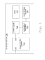
- Fig.1 is a block diagram of a power control system 110 of a first embodiment.
- the power control system 110 is adopted in a computer device 100 which can be but not limited to a desktop computer, a notebook computer, an electronic pad device, or a high-speed electronic, magnetic, optical or electronic chemical data processing unit with functions of processing logic operations and/or algorithmic operations, storage, data input and data output.
- the computer device 100 of the first embodiment includes the power control system 110, a power supply 120, an embedded controller 130, a central processing unit 140 and a south-bridge chipset 150.
- the power supply 120 is coupled to the embedded controller 130.
- the power supply 120 provides power to the embedded controller 130 for the operation thereof.
- the power control system 110 of the first embodiment includes a switch input terminal 115 and a logic output terminal 116.
- the switch input terminal 115 receives a trigger signal from a component of the computer device 100 to change a state of the computer device, for example changing from a normal state to a suspend-to-RAM state, a suspend-to-disc state, or a shutdown state.
- Said component could be but not limit to an external push-button or an external dual in-line package switch or an internal timer.
- the trigger signal could be but not limit to a pulse with a finite width or a digital logic signal.
- the logic output terminal 116 is coupled to the power supply 120 and performs on-off control of the power supply 120. That is, when the power supply 120 receives an enabling signal from the logic output terminal 116, the power supply 120 turns on and provides required power to the embedded controller 130, then the embedded controller begins initialization. After finishing initialization, the embedded controller 130 executes other default processes such as informing the south-bridge chipset 150 which is in charge of the power management of the computer device 100 to provide required power to the central processing unit 140. And when there's a disabling signal on the logic output terminal 116, the power supply 120 shuts down and further stops required power for the embedded controller 130 to further save the unnecessary power consumption.
- the logic output terminal 116 turns on or turns off the power supply 120 accordingly to provide or stop power to the embedded controller 120 and further optimizes the power consumption of the computer device 100.
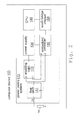
- Fig.2 is a block diagram of a power control system 110 of a second embodiment for the computer device 100.
- Fig.3 is a flow chart of a power control method for a computer device in the second embodiment.
- the power control system 110 of the second embodiment includes a first latch 111, an enabling logic 113, a switch input terminal 115 and a logic output terminal 116.
- the embedded controller 130 includes a first input terminal 171, a first output terminal 161 and a second output terminal 162.
- the switch input terminal 115 is in charge of receiving a trigger signal coming from a device switch component 200.
- the device switch component 200 can be but not limited to an external component such as a push-button or a dual in-line package switch, or an internal component like a timer.
- the trigger signal indicates the computer device to change a state, such as changing from a normal state to a suspend-to-RAM state, a suspend-to-disc state, or a shutdown state.
- the trigger signal can be but not limited to a pulse with a finite width or a digital logic signal.
- the first latch 111 includes a first enabling input terminal 311, a first latch output terminal 312 and a first reset terminal 313.
- the first enabling input terminal 311 is coupled to the switch input terminal 115.
- the first latch output terminal 312 is coupled to the first input terminal 171.
- the first reset terminal 313 is coupled to the second output terminal 162.
- the enabling logic 113 includes a first logic input terminal 331, a second logic input terminal 332 and a logic output terminal 116.
- the first logic input terminal 331 is coupled to the first latch output terminal 312.
- the second logic input terminal 332 is coupled to the first output terminal 161.
- the logic output terminal 116 is coupled to the power supply 120 and performs on-off control of the power supply 120.
- the enabling logic 113 When any one of the input terminals of the control logic 113 receives the second logic level, the enabling logic 113 outputs an enabling signal through the logic output terminal 116 and turns on the power supply 120. And when all the input terminals of the enabling logic 113 receive the first logic level, the enabling logic 113 outputs a disabling signal and turns off the power supply 120.
- the implementation of the enabling logic 113 can be but not limited to a NOR logic gate.
- the operation of the power control system 110 and the embedded controller 130 is described as follows.
- the power supply 120 is turned off and does not provide power to the embedded controller 130 (step 401 of Fig. 3 ).
- the switch input terminal 115 of the power control system 110 is in charge of detecting a trigger signal coming from an electronic signal of an external component or a timer in the computer device 100, wherein the timer may execute a real-time-clock process for waking up the computer device 100 (step 402 of Fig. 3 ).
- the first latch 111 sends the second logic level to the enabling logic 113 and generates a first input signal on the first input terminal 171.
- the enabling logic 113 outputs an enabling signal accordingly to turn on the power supply 120 to provide power to the embedded controller 130 (step 403 of Fig. 3 ).
- the embedded controller 130 is then initialized (step 404 of Fig. 3 ). After finishing initialization, the embedded controller 130 outputs the second logic level on the first output terminal 161 for notifying the enabling logic 113 of keeping the enabling signal.
- the embedded controller 130 also detects the first input signal on the first input terminal 171 (step 405 of Fig. 3 ).
- the embedded controller 130 then outputs a reset signal on the second output terminal 162 to reset the output of the first latch 111 to the first logic level, that is, to reset the first input signal. Meanwhile the embedded controller 130 executes a power-on process of the computer device 100 and informs the south-bridge chipset 150 to provide power to the central processing unit 140. The computer device 100 is then in the normal state (step 406 of Fig. 3 ).
- the switch input terminal 115 is in charge of detecting a trigger signal coming from the electronic signal of the external component or the timer in the computer device 100 wherein the timer may execute a real-time-clock process for shutting down the computer device 100 (step 407 of Fig.3 ).
- the first latch 111 outputs the second logic level to the first input terminal 171 for notifying the embedded controller 130 of executing a default process which changes the state of the computer device 100 to the suspend-to-RAM state, the suspend-to-disc state, or the shutdown state (step 408 of Fig.3 ).
- the embedded controller 130 After the default process is finished the embedded controller 130 outputs a reset signal on the second output terminal 162 to reset the output of the first latch 111 to the first logic level. Meanwhile the embedded controller 130 outputs the first logic level on the first output terminal 161 for notifying the enabling logic 113 of stopping keeping the enabling signal and outputting a disabling signal to turn off the power supply 120 and stop power of the embedded controller 130 to save the unnecessary power consumption (step 409 of Fig.3 ).
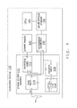
- Fig. 4 is a block diagram of a power control system 110 of a third embodiment adopted in the computer device 100.
- Fig. 5 is a flow chart of a power control method for a computer device of a third embodiment.
- the power control system 110 of the third embodiment further includes a third logic input terminal 333, an external power supply detecting circuit 112 and a second latch 114. It is noted that the third logic input terminal 333 is the third input terminal of the enabling logic 113.
- the external power supply detecting circuit 112 has a detecting output terminal 181.
- the external power supply detecting circuit 112 detects an external power supply, for example an external power supply plugged to the computer device 100 and enabled, it outputs an indication signal through the detecting output terminal 181.
- the external power supply can be but not limited to a power adaptor or a mobile charger, and the indication signal can be but not limited to a pulse with a finite width or a digital logic signal.
- the second latch 114 has a second enabling input terminal 341, a second latch output terminal 342 and a second reset terminal 343.
- the second enabling input terminal 341 is coupled to the detecting output terminal 181.
- the second reset terminal 343 is coupled to the second output terminal 162.
- the second latch output terminal 342 is coupled to the second input terminal 172 and the third logic input terminal 333.
- the second enabling terminal 341 receives the indication signal
- the second latch output terminal 342 outputs the second logic level.
- the second reset terminal 343 receives the reset signal
- the second latch output terminal 342 output the first logic level.
- the second latch 114 and the external power supply detecting circuit 112 can be incorporated into a single component in practice. However, in this embodiment, the second latch 114 serves as an independent component for maintaining the indication signal.
- the enabling logic 113 has three input terminals and functions the same as that in the second embodiment. That is, when any one of the input terminals of the control logic 113 receives the second logic level, the enabling logic 113 outputs an enabling signal through the logic output terminal 116 and turns on the power supply 120. And when all the input terminals of the enabling logic 113 receive the first logic level, the enabling logic 113 outputs a disabling signal and turns off the power supply 120.
- Fig. 4 besides the disclosed operation in the second embodiment (the flow chart disclosed in Fig. 3 ), further operation and functions of the power control system 110 and the embedded controller 130 are disclosed in the third embodiment as in the following descriptions.
- the power supply 120 is shut down and does not provide power to the embedded controller 130 (step 501 of Fig. 5 ).
- the external power supply detecting circuit 112 is in charge of detecting an external power supply (step 502 of Fig. 5 ).
- the external power supply detecting circuit 112 detects an external power supply, for example an external power supply plugged to the computer device 100 and enabled, it sends an indication signal through the detecting output terminal 181 to the second latch 114.
- the second latch 114 After receiving the indication signal, the second latch 114 sends the second logic level to the third logic input terminal 333 and generates a second input signal on the second input terminal 172.
- the enabling logic 133 then outputs an enabling signal accordingly to turn on the power supply 120 which supplies power to the embedded controller 130 (step 503 of Fig. 5 ).
- the embedded controller is then turned on and initialized (step 504 of Fig. 5 ). After finishing initialization the first output terminal 161 outputs the second logic level to render the enabling logic 113 keeping the enabling signal.
- the second input signal is generated on the second input terminal 172 (step 505 of Fig. 5 ).
- the embedded controller 130 then outputs a reset signal through the second output terminal 162 to reset the output of the second latch 114 to the first logic level, that is, to reset the second input signal (step 506 of Fig. 5 ).
- a default process for example determining if a battery of the computer device 100 should be charged to one hundred percentages, is executed (step 501 of Fig. 7). If charging should be proceeded, the computer device 100 charges the battery to one hundred percentages with the external power supply (step 508 of Fig. 5 ).
- the embedded controller 130 If charging should not be proceeded or the battery has been charged to one hundred percentages, the embedded controller 130 outputs the first logic level through the first output terminal 161 to render the enabling logic 113 stopping keeping the enabling signal to turn off the power supply 120 and stop the power of the embedded controller 130 (step 509 of Fig. 5 ). Thus saves unnecessary current consumption.
- Fig.6 is a flow chart of operations of an embedded controller of a power control system.
- the flow chart illustrates the power control method of the third embodiment and can be adopted for implementing the firmware code of the embedded controller.
- the power control method comprises the following steps (steps 601-611).
- step 601 the embedded controller starts and then finishes initialization.
- the step corresponds to the operation that the power control system outputs an enabling signal to turn on the power supply providing power to the embedded controller.
- the embedded controller outputs a first signal for notifying the power control system of keeping the enabling signal.
- the embedded controller detects if a first input signal or a second input signal exists.
- the step determines which signal turns on the computer device and the following actions are executed correspondingly.
- step 604 if the embedded controller detects the first input signal, the action as that in step 406 of Fig. 3 is executed.
- step 605 the embedded controller keep detecting the first signal, and if the first signal is not detected, go back to step 604.
- step 606 the action as that in step 408 of Fig. 3 is executed.
- step 607 the action as that in step 409 of Fig. 3 is executed.
- step 608 if the embedded controller detects the second input signal, the action as that in step 506 of Fig. 5 is executed.
- step 609 the action as that in step 507 of Fig. 5 is executed.
- step 610 the action as that in step 508 of Fig. 5 is executed.
- step 611 the action as that in step 509 of Fig. 5 is executed.
- This disclosure is advantageous because by a power control system controlling a power supply in a computer device, a power of an embedded controller in the computer device is either not supplied when not on duty or supplied to maintain the normal operation of the computer device such as power-on of the computer device or a specific process like charging a battery by an external power supply.
- a power of an embedded controller in the computer device is either not supplied when not on duty or supplied to maintain the normal operation of the computer device such as power-on of the computer device or a specific process like charging a battery by an external power supply.
- the power consumption of the computer device can be effectively decreased when the computer device is in a suspend-to-RAM mode, a suspend-to-disc mode, or a shutdown mode.
- the computer device is advantageous to comply with energy standards regulated all around the world, and the long stand-by time is also a strong feature for an electronic product.
Landscapes
- Engineering & Computer Science (AREA)
- Theoretical Computer Science (AREA)
- General Engineering & Computer Science (AREA)
- Physics & Mathematics (AREA)
- General Physics & Mathematics (AREA)
- Computer Hardware Design (AREA)
- Computing Systems (AREA)
- Power Sources (AREA)
- Direct Current Feeding And Distribution (AREA)
Applications Claiming Priority (1)
| Application Number | Priority Date | Filing Date | Title |
|---|---|---|---|
| TW101143362A TWI475368B (zh) | 2012-11-21 | 2012-11-21 | 電源控制系統及其方法 |
Publications (2)
| Publication Number | Publication Date |
|---|---|
| EP2735936A2 true EP2735936A2 (fr) | 2014-05-28 |
| EP2735936A3 EP2735936A3 (fr) | 2016-07-06 |
Family
ID=48692250
Family Applications (1)
| Application Number | Title | Priority Date | Filing Date |
|---|---|---|---|
| EP13170951.1A Withdrawn EP2735936A3 (fr) | 2012-11-21 | 2013-06-06 | Système de commande de puissance et procédé de commande de puissance |
Country Status (4)
| Country | Link |
|---|---|
| US (1) | US9411402B2 (fr) |
| EP (1) | EP2735936A3 (fr) |
| CN (1) | CN103838349B (fr) |
| TW (1) | TWI475368B (fr) |
Families Citing this family (14)
| Publication number | Priority date | Publication date | Assignee | Title |
|---|---|---|---|---|
| TWI546655B (zh) * | 2014-01-10 | 2016-08-21 | 瑞昱半導體股份有限公司 | 電子裝置、功能單元及其關機方法 |
| JP2015176214A (ja) * | 2014-03-13 | 2015-10-05 | 株式会社東芝 | 通信装置 |
| US9690955B2 (en) * | 2014-06-18 | 2017-06-27 | Texas Instruments Incorporated | Tunneling messages over an USB to control power delivery |
| CN104092451B (zh) * | 2014-06-18 | 2017-01-25 | 无锡芯响电子科技有限公司 | 一种功耗切换控制电路 |
| TWI547796B (zh) * | 2014-11-13 | 2016-09-01 | 鴻海精密工業股份有限公司 | 主機板供電電路 |
| CN105652995A (zh) * | 2014-11-13 | 2016-06-08 | 鸿富锦精密工业(武汉)有限公司 | 主板供电电路 |
| US9946600B2 (en) * | 2016-02-03 | 2018-04-17 | Mitac Computing Technology Corporation | Method of detecting power reset of a server, a baseboard management controller, and a server |
| CN108196481B (zh) * | 2018-01-02 | 2021-08-17 | 联想(北京)有限公司 | 一种供电调节方法和电子设备 |
| CN108258757B (zh) * | 2018-01-02 | 2023-05-02 | 联想(北京)有限公司 | 一种控制方法及设备 |
| CN108073422A (zh) * | 2018-01-03 | 2018-05-25 | 苏州三星电子电脑有限公司 | 计算机状态控制方法与计算机状态控制装置 |
| TWI672704B (zh) * | 2018-08-14 | 2019-09-21 | 華邦電子股份有限公司 | 記憶體裝置以及記憶體控制方法 |
| KR102627943B1 (ko) * | 2018-12-13 | 2024-01-22 | 삼성전자주식회사 | 반도체 회로 및 반도체 회로의 레이아웃 시스템 |
| WO2022126402A1 (fr) * | 2020-12-16 | 2022-06-23 | 华为技术有限公司 | Procédé d'économie d'énergie de dispositif de réseau et dispositif de réseau |
| CN115061562A (zh) * | 2022-06-27 | 2022-09-16 | 南昌华勤电子科技有限公司 | 一种ec功耗分级控制装置及方法、电子设备、存储介质 |
Family Cites Families (11)
| Publication number | Priority date | Publication date | Assignee | Title |
|---|---|---|---|---|
| DE69826172T2 (de) * | 1997-04-30 | 2005-02-03 | Fidelix Y.K., Kiyose | Stromversorgungsgerät |
| TWI224255B (en) * | 2002-10-24 | 2004-11-21 | Behavior Tech Computer Corp | Power-saving method and power-saving circuit for changing electronic apparatus with non-power-saving processor into power saving |
| US7523323B2 (en) * | 2005-09-15 | 2009-04-21 | Intel Corporation | Method and apparatus for quick resumption |
| US7602222B2 (en) * | 2005-09-30 | 2009-10-13 | Mosaid Technologies Incorporated | Power up circuit with low power sleep mode operation |
| TWI325533B (en) * | 2006-12-13 | 2010-06-01 | Compal Electronics Inc | Power control ststem and method |
| CN101582645B (zh) * | 2008-05-16 | 2012-03-14 | 群康科技(深圳)有限公司 | 电源电路及电源电路控制方法 |
| WO2010087855A1 (fr) * | 2009-01-30 | 2010-08-05 | Hewlett-Packard Development Company, L.P. | Commande de rail d'alimentation auxiliaire à l'état hors tension de système d'ordinateur |
| US20110185208A1 (en) * | 2010-01-28 | 2011-07-28 | Apple Inc. | Memory power reduction in a sleep state |
| TWI529521B (zh) * | 2010-02-10 | 2016-04-11 | 和碩聯合科技股份有限公司 | 電源管理方法及應用其的可攜式電子裝置 |
| TWI582575B (zh) * | 2011-03-17 | 2017-05-11 | 和碩聯合科技股份有限公司 | 電子裝置 |
| TWI461897B (zh) * | 2011-11-16 | 2014-11-21 | Wistron Corp | 電源控制裝置及電子裝置 |
-
2012
- 2012-11-21 TW TW101143362A patent/TWI475368B/zh active
-
2013
- 2013-03-06 CN CN201310070666.XA patent/CN103838349B/zh active Active
- 2013-06-06 EP EP13170951.1A patent/EP2735936A3/fr not_active Withdrawn
- 2013-11-14 US US14/080,310 patent/US9411402B2/en active Active
Non-Patent Citations (1)
| Title |
|---|
| None |
Also Published As
| Publication number | Publication date |
|---|---|
| CN103838349A (zh) | 2014-06-04 |
| EP2735936A3 (fr) | 2016-07-06 |
| US20140143574A1 (en) | 2014-05-22 |
| TW201421223A (zh) | 2014-06-01 |
| US9411402B2 (en) | 2016-08-09 |
| TWI475368B (zh) | 2015-03-01 |
| CN103838349B (zh) | 2016-09-07 |
Similar Documents
| Publication | Publication Date | Title |
|---|---|---|
| US9411402B2 (en) | Power control system and power control method | |
| US5230074A (en) | Battery operated computer power management system | |
| US8407495B2 (en) | Information processor and power supply method for an information processor | |
| US20110131427A1 (en) | Power management states | |
| US8601302B2 (en) | Processor system in low power state retention mode with linear regulator off and switch regulator low in power management IC | |
| JP3974510B2 (ja) | コンピュータ装置、電力管理方法、およびプログラム | |
| US10891062B2 (en) | Managing host communication with a regulator in a low power mode | |
| US20140089697A1 (en) | System-on-chip with capability for controlling power supply according to data transaction and method of operating the same | |
| US9568983B1 (en) | Power cut off mode for conserving power in electronic devices | |
| EP2791758B1 (fr) | Mise en uvre d'un état hors tension dans un dispositif informatique | |
| JP2004152304A (ja) | Ac電源障害の場合にスタンバイ状態にあるパーソナルコンピュータの状態データを保持するためのシステムおよび方法 | |
| EP2843502B1 (fr) | Dispositif de traitement d'informations, procédé de traitement d'informations, et programme | |
| JP6409240B1 (ja) | 情報処理装置、制御方法、及びプログラム | |
| US20110060923A1 (en) | Port Power Control | |
| CN103970253B (zh) | 省电操作方法与电子装置 | |
| Jenkins | Decrease power consumption using a programmable logic device |
Legal Events
| Date | Code | Title | Description |
|---|---|---|---|
| PUAI | Public reference made under article 153(3) epc to a published international application that has entered the european phase |
Free format text: ORIGINAL CODE: 0009012 |
|
| 17P | Request for examination filed |
Effective date: 20130606 |
|
| AK | Designated contracting states |
Kind code of ref document: A2 Designated state(s): AL AT BE BG CH CY CZ DE DK EE ES FI FR GB GR HR HU IE IS IT LI LT LU LV MC MK MT NL NO PL PT RO RS SE SI SK SM TR |
|
| AX | Request for extension of the european patent |
Extension state: BA ME |
|
| PUAL | Search report despatched |
Free format text: ORIGINAL CODE: 0009013 |
|
| AK | Designated contracting states |
Kind code of ref document: A3 Designated state(s): AL AT BE BG CH CY CZ DE DK EE ES FI FR GB GR HR HU IE IS IT LI LT LU LV MC MK MT NL NO PL PT RO RS SE SI SK SM TR |
|
| AX | Request for extension of the european patent |
Extension state: BA ME |
|
| RIC1 | Information provided on ipc code assigned before grant |
Ipc: G06F 1/32 20060101AFI20160531BHEP Ipc: G06F 1/26 20060101ALI20160531BHEP |
|
| R17P | Request for examination filed (corrected) |
Effective date: 20161208 |
|
| RBV | Designated contracting states (corrected) |
Designated state(s): AL AT BE BG CH CY CZ DE DK EE ES FI FR GB GR HR HU IE IS IT LI LT LU LV MC MK MT NL NO PL PT RO RS SE SI SK SM TR |
|
| 17Q | First examination report despatched |
Effective date: 20170622 |
|
| GRAP | Despatch of communication of intention to grant a patent |
Free format text: ORIGINAL CODE: EPIDOSNIGR1 |
|
| INTG | Intention to grant announced |
Effective date: 20180308 |
|
| STAA | Information on the status of an ep patent application or granted ep patent |
Free format text: STATUS: THE APPLICATION IS DEEMED TO BE WITHDRAWN |
|
| 18D | Application deemed to be withdrawn |
Effective date: 20180719 |