EP2733765A1 - Organic light emitting diode display device - Google Patents
Organic light emitting diode display device Download PDFInfo
- Publication number
- EP2733765A1 EP2733765A1 EP20130190980 EP13190980A EP2733765A1 EP 2733765 A1 EP2733765 A1 EP 2733765A1 EP 20130190980 EP20130190980 EP 20130190980 EP 13190980 A EP13190980 A EP 13190980A EP 2733765 A1 EP2733765 A1 EP 2733765A1
- Authority
- EP
- European Patent Office
- Prior art keywords
- light emitting
- organic light
- emitting diode
- electrode
- diode display
- Prior art date
- Legal status (The legal status is an assumption and is not a legal conclusion. Google has not performed a legal analysis and makes no representation as to the accuracy of the status listed.)
- Granted
Links
Images


Classifications
-
- H—ELECTRICITY
- H10—SEMICONDUCTOR DEVICES; ELECTRIC SOLID-STATE DEVICES NOT OTHERWISE PROVIDED FOR
- H10K—ORGANIC ELECTRIC SOLID-STATE DEVICES
- H10K59/00—Integrated devices, or assemblies of multiple devices, comprising at least one organic light-emitting element covered by group H10K50/00
- H10K59/80—Constructional details
- H10K59/805—Electrodes
- H10K59/8052—Cathodes
- H10K59/80523—Multilayers, e.g. opaque multilayers
-
- H—ELECTRICITY
- H10—SEMICONDUCTOR DEVICES; ELECTRIC SOLID-STATE DEVICES NOT OTHERWISE PROVIDED FOR
- H10K—ORGANIC ELECTRIC SOLID-STATE DEVICES
- H10K50/00—Organic light-emitting devices
- H10K50/80—Constructional details
-
- H—ELECTRICITY
- H10—SEMICONDUCTOR DEVICES; ELECTRIC SOLID-STATE DEVICES NOT OTHERWISE PROVIDED FOR
- H10K—ORGANIC ELECTRIC SOLID-STATE DEVICES
- H10K50/00—Organic light-emitting devices
- H10K50/80—Constructional details
- H10K50/805—Electrodes
- H10K50/81—Anodes
- H10K50/814—Anodes combined with auxiliary electrodes, e.g. ITO layer combined with metal lines
-
- H—ELECTRICITY
- H10—SEMICONDUCTOR DEVICES; ELECTRIC SOLID-STATE DEVICES NOT OTHERWISE PROVIDED FOR
- H10K—ORGANIC ELECTRIC SOLID-STATE DEVICES
- H10K50/00—Organic light-emitting devices
- H10K50/80—Constructional details
- H10K50/805—Electrodes
- H10K50/82—Cathodes
-
- H—ELECTRICITY
- H10—SEMICONDUCTOR DEVICES; ELECTRIC SOLID-STATE DEVICES NOT OTHERWISE PROVIDED FOR
- H10K—ORGANIC ELECTRIC SOLID-STATE DEVICES
- H10K50/00—Organic light-emitting devices
- H10K50/80—Constructional details
- H10K50/805—Electrodes
- H10K50/82—Cathodes
- H10K50/824—Cathodes combined with auxiliary electrodes
-
- H—ELECTRICITY
- H10—SEMICONDUCTOR DEVICES; ELECTRIC SOLID-STATE DEVICES NOT OTHERWISE PROVIDED FOR
- H10K—ORGANIC ELECTRIC SOLID-STATE DEVICES
- H10K50/00—Organic light-emitting devices
- H10K50/80—Constructional details
- H10K50/805—Electrodes
- H10K50/82—Cathodes
- H10K50/826—Multilayers, e.g. opaque multilayers
-
- H—ELECTRICITY
- H10—SEMICONDUCTOR DEVICES; ELECTRIC SOLID-STATE DEVICES NOT OTHERWISE PROVIDED FOR
- H10K—ORGANIC ELECTRIC SOLID-STATE DEVICES
- H10K2102/00—Constructional details relating to the organic devices covered by this subclass
-
- H—ELECTRICITY
- H10—SEMICONDUCTOR DEVICES; ELECTRIC SOLID-STATE DEVICES NOT OTHERWISE PROVIDED FOR
- H10K—ORGANIC ELECTRIC SOLID-STATE DEVICES
- H10K50/00—Organic light-emitting devices
- H10K50/80—Constructional details
- H10K50/84—Passivation; Containers; Encapsulations
-
- H—ELECTRICITY
- H10—SEMICONDUCTOR DEVICES; ELECTRIC SOLID-STATE DEVICES NOT OTHERWISE PROVIDED FOR
- H10K—ORGANIC ELECTRIC SOLID-STATE DEVICES
- H10K50/00—Organic light-emitting devices
- H10K50/80—Constructional details
- H10K50/84—Passivation; Containers; Encapsulations
- H10K50/841—Self-supporting sealing arrangements
-
- H—ELECTRICITY
- H10—SEMICONDUCTOR DEVICES; ELECTRIC SOLID-STATE DEVICES NOT OTHERWISE PROVIDED FOR
- H10K—ORGANIC ELECTRIC SOLID-STATE DEVICES
- H10K59/00—Integrated devices, or assemblies of multiple devices, comprising at least one organic light-emitting element covered by group H10K50/00
- H10K59/80—Constructional details
- H10K59/87—Passivation; Containers; Encapsulations
- H10K59/871—Self-supporting sealing arrangements
Definitions
- the invention relates in general to an organic light emitting diode display device, and particularly to an organic light emitting diode display device comprising an electrode having two portions, wherein the ratios of an alkaline earth element to silver in the two portions are different.
- Organic light emitting diode display devices have become one of the most important research targets of display technology due to light weights, good display properties, and low costs. Therefore, the requirements to the functions and characteristics of organic light emitting diode display devices have gradually increased as well.
- the organic light emitting diode structure of an organic light emitting diode display device is mainly comprised of two electrodes and an organic light emitting layer disposed between the two electrodes.
- a voltage is applied on the two electrodes, charge carriers are produced and pass through the organic light emitting layer, and the charge carriers combined produce lights.
- the electrodes located inside the organic light emitting display device is formed on the light emitting layer made of organic materials.
- the reliability and luminous efficiency of the whole display device may be influenced due to the poor adhesion between the electrodes and the organic light emitting layer. Therefore, researchers have been working on providing an organic light emitting diode display device with high reliability and great luminous efficiency.
- the invention relates to an organic light emitting diode display device.
- the organic light emitting diode display device with an electrode having two portions, wherein the ratios of an alkaline earth element to silver in the two portions are different, luminous efficiency can be increased, the adhesion between the electrodes and an organic light emitting layer is improved, and the conductivity of the electrodes are increased.
- an organic light emitting diode (OLED) display device comprising a first substrate, a first electrode, an organic light emitting layer, a second electrode, and a second substrate.
- the first electrode is disposed on the first substrate.
- the organic light emitting layer is disposed on the first electrode.
- the second electrode is disposed on the organic light emitting layer.
- the second substrate is located on the second electrode.
- the material of the second electrode comprises an alkaline earth element and silver.
- the second electrode comprises a first portion and a second portion, and the first portion is located between the second portion and the first substrate. The ratios of the alkaline earth element to silver in the first portion and in the second portion are different.
- FIG. 1 shows an explosion diagram of an organic light emitting diode display device according to an embodiment of the present disclosure
- FIG. 2 shows a schematic diagram of the organic light emitting display panel according to an embodiment of the present disclosure
- FIG. 3 shows an organic light emitting diode display panel according to another embodiment of the present disclosure
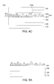
- FIGS. 4A-4C illustrate a process for manufacturing an organic light emitting diode display panel according to an embodiment of the present disclosure.
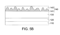
- FIGS. 5A-5B illustrate a process of an organic light emitting diode display panel according to another embodiment of the present disclosure.
- an organic light emitting diode display device is provided.
- the organic light emitting diode display device with an electrode having two portions, wherein the ratios of an alkaline earth element to silver in the two portions are different, luminous efficiency can be increased, the adhesion between the electrodes and an organic light emitting layer is improved, and the conductivity of the electrodes are increased.
- FIG. 1 shows an explosion diagram of an organic light emitting diode display device 10 according to an embodiment of the present disclosure.
- the organic light emitting diode display device 10 comprises an organic light emitting display panel 100, a case 200, and a front plate 300.
- the organic light emitting display panel 100 is disposed in the case 200.
- the organic light emitting display panel 100 is connected to driving units (not shown) for receiving driving signals.
- the front plate 300 is also disposed in the case 200.
- the front plate 300 is located between the organic light emitting display panel 100 and observers.
- the front plate 300 being a transparent cover plate can provide protection, resistance to pressure, and stain resistance.
- the front plate 300 can further comprise functional structures, such as touch sensors, or barriers or lens for three-dimensional displaying.
- the case 200 comprises an upper case 200A and a lower case 200B.
- the organic light emitting display panel 100 and the front plate 300 are disposed between the upper case 200A and the lower case 200B.
- the front plate 300 can be removed.
- FIG. 2 shows a schematic diagram of the organic light emitting display panel 100 according to an embodiment of the present disclosure.
- the organic light emitting display panel 100 comprises a first substrate 110, a first electrode 120, an organic light emitting layer 130, a second electrode 140, and a second substrate 150.
- the first electrode 120 regard as anode is disposed on the first substrate 110 and is located between the first substrate 110 and the second substrate 150.
- the organic light emitting display panel 100 may further comprise additional structures, such as thin film transistors (TFT), conductive lines, capacitors, dielectric layers, pixel definition layers, and etc., between the first substrate 110 and the first electrode 120, and the description of those structures and the driving operations thereof are omitted herein.
- TFT thin film transistors
- the organic light emitting layer 130 is disposed on the first electrode 120 and is located between the first electrode 120 and the second substrate 150.
- the electrodes on two sides of the organic light emitting layer 130 regard as cathode and anode to produce electron-hole pairs with a voltage applied thereon, and the electrons and holes combine in the light emitting layer for emitting lights.
- the second electrode 140 is disposed on the organic light emitting layer 130 and is located between the organic light emitting layer 130 and the first electrode 120. There is usually a gap between the second substrate 150 and the second electrode 140; however, the second substrate 150 and the second electrode 140 can also be contacted to each other.
- a capping layer (not shown) can further be disposed on the second electrode 140 to fully cover the first electrode 120, the organic light emitting layer 130, and the second electrode 140 for preventing water and oxygen from passing through, such that the life of the organic light emitting diodes can be prolonged.
- the first substrate 110 and the second substrate 150 can be sealed with encapsulating materials, such as frits (not shown) or sealants (not shown) connecting the first substrate 110 and the second substrate 150 for enclosing a space, in which space the organic light emitting diodes are disposed.
- an optical cement adhesive (OCA, not shown) can be filled in the space and occupy part of the space where the organic light emitting diodes do not occupy, such that chances of the organic light emitting diodes being damaged under pressure are reduced.
- the materials of the first substrate 110 and the second substrate 150 can be glass, plastics, acrylates, ceramics, metals, or the composite structure thereof.
- the substrate (either the first substrate 110 or the second substrate 150) disposed on the light emitting surface needs to be light transmissive.
- the material of the first electrode 120 comprises a transparent conductive material, such as indium tin oxide (ITO), and silver (or aluminum), and indium tin oxide and silver form a composite stacked structure, such as ITO-Ag-ITO.
- ITO indium tin oxide
- silver can reduce resistance and can be used as a reflective layer.
- the material of the second electrode 140 comprises an alkaline earth element and silver (aluminum may apply as well). In this embodiment, the second electrode 140 is located on the light emitting surface; therefore, the thickness of the second electrode needs to be controlled in order for lights to pass through.
- the second electrode 140 comprises a first portion 141 and a second portion 143, the ratios of the alkaline earth element to silver in the first portion 141 and in the second portion 143 are different.
- the first portion 141 of the second electrode 140 is such as located between the second portion 143 of the second electrode 140 and the first substrate 110.
- the interface 140a between the first portion 141 and the second portion 143 has such as an irregular shape.
- the interface between the first portion 141 and the second portion 143 can also be flat (not shown), and the first portion 141 and the second portion 143 are two stacked planar films.
- the organic light emitting layer 130 comprises such as electron transport layer (ETL)/ electron injection layer (EIL), emission layer (EML), and hole transport layer (HTL)/hole injection layer (HIL).
- ETL electron transport layer
- EIL electron injection layer
- EML emission layer
- HTL hole transport layer
- HIL hole injection layer
- the emission layer is disposed between the electron transport layer/electron injection layer and the hole transport layer/hole injection layer (not shown).
- the material of the electron transport layer and the material of the electron injection layer comprise, for example, BPhen (4,7-diphenyl-1,10-phenanthroline), Liq (8-hydroxyquinolinolato-lithium), BALq (Bis(2-methyl-8-quinolinolate)-4-(phenylphenolato)aluminium), TPBi (2,2',2"-(1,3,5-benzinetriyl)-tris(1-phenyl-1-H-benzimidazole), or the combinations thereof.
- the material of the electron injection layer further comprises lithium (Li) or cesium (Cs) dopants.
- the material of the hole transport layer comprises, such as, NPB (N,N'-bis(naphthalen-1-yl)-N,N'-bis(phenyl)-benzidine), TPD (N,N'-bis(3-methylphenyl)-N,N'-bis(phenyl)-benzidine), ⁇ -NPD (N,N'-bis(naphthalen-1-yl)-N,N'-bis(phenyl)-2,2'-dimethylbenzidine), or the combinations thereof.
- NPB N,N'-bis(naphthalen-1-yl)-N,N'-bis(phenyl)-benzidine
- TPD N,N'-bis(3-methylphenyl)-N,N'-bis(phenyl)-benzidine
- ⁇ -NPD N,N'-bis(naphthalen-1-yl)-N,N'-bis(phenyl)-2,2'-dimethylbenzidine
- the material of the hole injection layer comprises, such as, HAT-CN (Dipyrazino[2,3-f:2',3'-h]quinoxaline-2,3,6,7,10,11-hexacarbonitrile), phthalocyanine copper complex (CuPC), F4-TCNQ (2,3,5,6-tetrafluoro-7,7,8,8-tetracyano-quinodimethane), or the combinations thereof.
- HAT-CN Dipyrazino[2,3-f:2',3'-h]quinoxaline-2,3,6,7,10,11-hexacarbonitrile
- CuPC phthalocyanine copper complex
- F4-TCNQ 2,3,5,6-tetrafluoro-7,7,8,8-tetracyano-quinodimethane
- the material of the light emitting layer may comprise fluorescence materials or phosphor materials of red light, green light, or blue light.
- the red fluorescence material comprises such as a mixture of rubrene and Alq 3 (Tris(8-hydroxy-quinolinato)aluminium) as the host material doped with DCJTB dye (4-(dicyanomethylene)-2-tert-butyl-6-(1,1,7,7-tetramethyljulolidin-4-yl-vinyl)-4H -pyran) as the guest material.
- the red phosphor material comprises such as CBP (4,4'-bis(carbazol-9-yl)biphenyl) and/or TCTA (4,4',4"-Tris(carbazol-9-yl)triphenylamine) as the host material doped with Ir(piq) 3 (Tris(1-phenylisoquinoline)iridium(III)) and/or Ir(btp) 2 (acac) (Bis(2-benzo[b]thiophen-2-yl-pyridine)(acetylacetonate)iridium(III)) as the guest material.
- CBP 4,4'-bis(carbazol-9-yl)biphenyl
- TCTA 4,4',4"-Tris(carbazol-9-yl)triphenylamine
- Ir(piq) 3 Tris(1-phenylisoquinoline)iridium(III)
- Ir(btp) 2 acac
- the green fluorescence material comprises such as TPBA (2,2'-bi(9,10-diphenyl-anthracene) as the host material doped with C545T (10-(2-Benzothiazolyl)-2,3,6,7-tetrahydro-1,1,7,7-tetramethyl-1H,5H,11H-(1)be nzopyropyrano(6,7-8-l,j)quinolizin-11-one) as the guest material.
- TPBA 2,2'-bi(9,10-diphenyl-anthracene
- C545T 10-(2-Benzothiazolyl)-2,3,6,7-tetrahydro-1,1,7,7-tetramethyl-1H,5H,11H-(1)be nzopyropyrano(6,7-8-l,j)quinolizin-11-one
- the green phosphor material comprises such as CBP (4,4'-bis(carbazol-9-yl)biphenyl) and/or TCTA (4,4',4"-Tris(carbazol-9-yl)triphenylamine) as the host material doped with Ir(ppy) 3 (Tris(2-phenylpyridine)iridium(III)) and/or Ir(ppy) 2 (acac) (Bis(2-phenylpyridine)(acetylacetonate)iridium(III)) as the guest material.
- CBP 4,4'-bis(carbazol-9-yl)biphenyl
- TCTA 4,4',4"-Tris(carbazol-9-yl)triphenylamine
- the blue fluorescence material comprises such as MADN (2-methyl-9,10-bis(naphthalen-2-yl)anthracene) as the host material doped with DPVABi (4,4'-bis[4-(di-p-tolylamino)styryl]biphenyl) as the guest material.
- the blue phosphot material comprises such as MCP (1,3-bis(carbazol-9-yl)benzene) and/or UGH-2 (1,4-bis(triphenylsilyl)benzene) as the host material doped with FlrPic (Bis(3,5-difluoro-2-(2-pyridyl)phenyl-(2-carboxypyridyl)iridium(III)) and/or Flr 6 (Bis(2,4-difluorophenylpyridinato)tetrakis(1-pyrazolyl)borate iridium(III)) as the guest material.
- FlrPic Bis(3,5-difluoro-2-(2-pyridyl)phenyl-(2-carboxypyridyl)iridium(III)
- Flr 6 Bis(2,4-difluorophenylpyridinato)tetrakis(1-pyrazolyl)borate iridium
- the first portion 141 of the second electrode 140 has a first thickness T1
- the second portion 143 of the second electrode 140 has a second thickness T2.
- the above-mentioned thicknesses are the average thicknesses of the corresponding portions.
- the ratio of the first thickness T1 to the second thickness T2 is, for example, 1:0.5-1:4.
- the ratio of the alkaline earth element to silver in the first portion 141 is larger than the ratio of the alkaline earth element to silver in the second portion 143.
- the alkaline earth element is such as magnesium or silver.
- the first portion 141 is formed of magnesium, and the second portion 143 is formed of silver. In another embodiment, the first portion 141 is formed of magnesium, and the second portion 143 is formed from magnesium and silver. In a further embodiment, the first portion 141 is formed from magnesium and silver, and the second portion 143 is formed of silver. In yet another embodiment, the first portion 141 is formed from magnesium and silver, and the second portion 143 is formed from magnesium and silver.
- the lowest unoccupied molecular orbital (LUMO) of the electron transport layer/electron injection layer of the organic light emitting layer 130 has a band gap (energy gap) value of 2.5-3.5 eV, the work function of magnesium is 3.46 eV, and the work function of magnesium-silver alloy if about 3.7 eV.
- the electron transport layer/electron injection layer of the organic light emitting layer 130 is in direct contact with the first portion 141 of the second electrode 140, and the work function of magnesium is close to the work function (band gap value) of the electron transport layer/electron injection layer, the magnesium content being relatively high in the first portion 141 is advantageous to the transport or injection of electrons, and hence the luminous efficiency is improved.
- the adhesion between pure magnesium and organic films is poor.
- the material of the second electrode 140 comprises magnesium and silver, and the existence of silver is beneficial to the adhesion between the second electrode 140 and the organic light emitting layer 130.
- the wave patterns of driving signals from ends of conductive lines tend to decay more quickly.
- the existence of silver can increase the conductivity of the second electrode 140, and therefore, the undesired changes of the wave patterns of driving signals are reduced.
- the atomic ratio of magnesium to the mixture of magnesium and silver is about between 80% and less than 100% (100%>Mg/(Mg+Ag) ⁇ 80%).
- the atomic ratio of magnesium to the mixture of magnesium and silver is about between 90% and less than 100% (100%>Mg/(Mg+Ag) ⁇ 90%).
- the atomic ratio of magnesium to the mixture of magnesium and silver is about between larger than 0% and 90% (90% ⁇ Mg/Mg+Ag)>0%).
- the atomic ratio of magnesium to the mixture of magnesium and silver is about between larger than 0% and 80% (80% ⁇ Mg/(Mg+Ag)>0%).
- FIG. 3 shows an organic light emitting diode display panel 100' according to another embodiment of the present disclosure.
- the second electrode 140 of the organic light emitting diode display panel 100' further comprises a third portion 260.
- the third portion 260 is located on the second portion 143.
- the third portion 260 is located between the second portion 143 and the second substrate 150.
- the material of the third portion 260 is silver.
- the silver in the third portion 260 can enhance the electron transport/injection properties of the whole electrode.
- the material of the second portion 143 is silver
- the third portion 260 can be optionally omitted.
- the elements in the present embodiment sharing the same labels with those in the previous embodiments are the same elements, and the description of which is omitted.
- FIGS. 4A-4C illustrate a process for manufacturing an organic light emitting diode display panel according to an embodiment of the present disclosure.
- the first substrate 110 is provided, the first electrode 120 is formed on the first substrate 110, and the organic light emitting layer 130 is formed on the first electrode 120.
- additional components such as thin film transistors and conductive lines, are omitted from the description of the above-mentioned steps.
- the second electrode 140 is formed on the organic light emitting layer 130.
- the second electrode 140 is formed by such as a thermal evaporation process.
- the first portion 141 and the second portion 143 of the second electrode 140 are formed in the same thermal evaporation process simultaneously.
- the ratios of the alkaline earth element to silver in the first portion 141 and in the second portion 143 are different.
- the first portion 141 and the second portion 143 are formed in the same thermal evaporation process.
- the interface 140a between the first portion 141 and the second portion 143 is more indefinite and less distinct, that is to say, the physical interface that can be observed by such as an electron microscopy is less clear.
- the first portion 141 and the second portion 143 are two stacked films, an area of the first portion 141 close to the organic light emitting layer 130 and an area of the second portion 143 close to the second substrate 150 still have different ratios of the alkaline earth element to silver.
- the second substrate 150 is disposed on the second substrate 150. As such, the organic light emitting diode display panel 100 as shown in FIG. 4C ( FIG. 2 ) is formed.
- FIGS. 5A-5B illustrate a process of an organic light emitting diode display panel according to another embodiment of the present disclosure. Please refer to FIG. 4 and FIGS. 5A-5B .
- the structure as shown in FIG. 4A is formed.
- the first portion 141 of the second electrode 140 is formed on the organic light emitting layer 130.
- the first portion 141 of the second electrode 140 is formed by such as a thermal evaporation process.
- the magnesium content in the first portion 141 is relatively high, and thus, an irregular structure as shown in FIG. 5A may be formed, and the first portion 141 has a surface of an irregular shape.
- the second portion 143 of the second electrode 140 is formed on the first portion 141.
- the second portion 143 of the second electrode 140 is formed by such as a thermal evaporation process.
- the silver content in the second portion 143 is relatively high, and thus, the film formation is greater, such that the second electrode 140 can be formed with a flat surface.
- the adhesion between the second electrode 140 and the organic light emitting layer 130 is increased.
- the second substrate 150 is disposed on the second electrode 140. As such, the organic light emitting diode display panel 100 as shown in FIG. 2 is formed.
Landscapes
- Physics & Mathematics (AREA)
- Optics & Photonics (AREA)
- Electroluminescent Light Sources (AREA)
Abstract
Description
- The invention relates in general to an organic light emitting diode display device, and particularly to an organic light emitting diode display device comprising an electrode having two portions, wherein the ratios of an alkaline earth element to silver in the two portions are different.
- Along with the advances of display technology, various types of display devices have been developed. Organic light emitting diode display devices have become one of the most important research targets of display technology due to light weights, good display properties, and low costs. Therefore, the requirements to the functions and characteristics of organic light emitting diode display devices have gradually increased as well.
- Generally, the organic light emitting diode structure of an organic light emitting diode display device is mainly comprised of two electrodes and an organic light emitting layer disposed between the two electrodes. When a voltage is applied on the two electrodes, charge carriers are produced and pass through the organic light emitting layer, and the charge carriers combined produce lights.
- However, the electrodes located inside the organic light emitting display device is formed on the light emitting layer made of organic materials. The reliability and luminous efficiency of the whole display device may be influenced due to the poor adhesion between the electrodes and the organic light emitting layer. Therefore, researchers have been working on providing an organic light emitting diode display device with high reliability and great luminous efficiency.
- The invention relates to an organic light emitting diode display device. In the organic light emitting diode display device, with an electrode having two portions, wherein the ratios of an alkaline earth element to silver in the two portions are different, luminous efficiency can be increased, the adhesion between the electrodes and an organic light emitting layer is improved, and the conductivity of the electrodes are increased.
- According to an aspect of the present disclosure, an organic light emitting diode (OLED) display device is provided. The organic light emitting diode display device comprises a first substrate, a first electrode, an organic light emitting layer, a second electrode, and a second substrate. The first electrode is disposed on the first substrate. The organic light emitting layer is disposed on the first electrode. The second electrode is disposed on the organic light emitting layer. The second substrate is located on the second electrode. The material of the second electrode comprises an alkaline earth element and silver. The second electrode comprises a first portion and a second portion, and the first portion is located between the second portion and the first substrate. The ratios of the alkaline earth element to silver in the first portion and in the second portion are different.
- The above and other aspects of the disclosure will become better understood with regard to the following detailed description of the non-limiting embodiment(s). The following description is made with reference to the accompanying drawings.
-
FIG. 1 shows an explosion diagram of an organic light emitting diode display device according to an embodiment of the present disclosure; -
FIG. 2 shows a schematic diagram of the organic light emitting display panel according to an embodiment of the present disclosure; -
FIG. 3 shows an organic light emitting diode display panel according to another embodiment of the present disclosure; -
FIGS. 4A-4C illustrate a process for manufacturing an organic light emitting diode display panel according to an embodiment of the present disclosure; and -
FIGS. 5A-5B illustrate a process of an organic light emitting diode display panel according to another embodiment of the present disclosure. - In the embodiments of the present disclosure, an organic light emitting diode display device is provided. In the organic light emitting diode display device, with an electrode having two portions, wherein the ratios of an alkaline earth element to silver in the two portions are different, luminous efficiency can be increased, the adhesion between the electrodes and an organic light emitting layer is improved, and the conductivity of the electrodes are increased. The following embodiments are for the purpose of elaboration only, not for limiting the scope of protection of the invention. Detailed structures and processes may be modified or changed by one skilled in the art after having the benefit of this description of the disclosure.
- Referring to
FIG. 1, FIG. 1 shows an explosion diagram of an organic light emittingdiode display device 10 according to an embodiment of the present disclosure. As shown inFIG. 1 , the organic light emittingdiode display device 10 comprises an organic lightemitting display panel 100, acase 200, and afront plate 300. The organic lightemitting display panel 100 is disposed in thecase 200. The organic lightemitting display panel 100 is connected to driving units (not shown) for receiving driving signals. Thefront plate 300 is also disposed in thecase 200. Thefront plate 300 is located between the organic lightemitting display panel 100 and observers. Thefront plate 300 being a transparent cover plate can provide protection, resistance to pressure, and stain resistance. Thefront plate 300 can further comprise functional structures, such as touch sensors, or barriers or lens for three-dimensional displaying. In the embodiment, as shown inFIG. 1 , thecase 200 comprises anupper case 200A and alower case 200B. The organic lightemitting display panel 100 and thefront plate 300 are disposed between theupper case 200A and thelower case 200B. In other embodiments, thefront plate 300 can be removed. - Referring to
FIG. 2, FIG. 2 shows a schematic diagram of the organic lightemitting display panel 100 according to an embodiment of the present disclosure. As shown inFIG. 2 , the organic lightemitting display panel 100 comprises afirst substrate 110, afirst electrode 120, an organiclight emitting layer 130, asecond electrode 140, and asecond substrate 150. Thefirst electrode 120 regard as anode is disposed on thefirst substrate 110 and is located between thefirst substrate 110 and thesecond substrate 150. The organic lightemitting display panel 100 may further comprise additional structures, such as thin film transistors (TFT), conductive lines, capacitors, dielectric layers, pixel definition layers, and etc., between thefirst substrate 110 and thefirst electrode 120, and the description of those structures and the driving operations thereof are omitted herein. The organiclight emitting layer 130 is disposed on thefirst electrode 120 and is located between thefirst electrode 120 and thesecond substrate 150. The electrodes on two sides of the organiclight emitting layer 130 regard as cathode and anode to produce electron-hole pairs with a voltage applied thereon, and the electrons and holes combine in the light emitting layer for emitting lights. Thesecond electrode 140 is disposed on the organiclight emitting layer 130 and is located between the organiclight emitting layer 130 and thefirst electrode 120. There is usually a gap between thesecond substrate 150 and thesecond electrode 140; however, thesecond substrate 150 and thesecond electrode 140 can also be contacted to each other. A capping layer (not shown) can further be disposed on thesecond electrode 140 to fully cover thefirst electrode 120, the organiclight emitting layer 130, and thesecond electrode 140 for preventing water and oxygen from passing through, such that the life of the organic light emitting diodes can be prolonged. Thefirst substrate 110 and thesecond substrate 150 can be sealed with encapsulating materials, such as frits (not shown) or sealants (not shown) connecting thefirst substrate 110 and thesecond substrate 150 for enclosing a space, in which space the organic light emitting diodes are disposed. Further, an optical cement adhesive (OCA, not shown) can be filled in the space and occupy part of the space where the organic light emitting diodes do not occupy, such that chances of the organic light emitting diodes being damaged under pressure are reduced. The materials of thefirst substrate 110 and thesecond substrate 150 can be glass, plastics, acrylates, ceramics, metals, or the composite structure thereof. The substrate (either thefirst substrate 110 or the second substrate 150) disposed on the light emitting surface needs to be light transmissive. - In the embodiment, the material of the
first electrode 120 comprises a transparent conductive material, such as indium tin oxide (ITO), and silver (or aluminum), and indium tin oxide and silver form a composite stacked structure, such as ITO-Ag-ITO. In the structure, silver can reduce resistance and can be used as a reflective layer. When thefirst electrode 120 is located on the light emitting surface, the thickness of the silver layer needs to be controlled in order for lights to pass through. The material of thesecond electrode 140 comprises an alkaline earth element and silver (aluminum may apply as well). In this embodiment, thesecond electrode 140 is located on the light emitting surface; therefore, the thickness of the second electrode needs to be controlled in order for lights to pass through. Thesecond electrode 140 comprises afirst portion 141 and asecond portion 143, the ratios of the alkaline earth element to silver in thefirst portion 141 and in thesecond portion 143 are different. In the embodiment, as shown inFIG. 2 , thefirst portion 141 of thesecond electrode 140 is such as located between thesecond portion 143 of thesecond electrode 140 and thefirst substrate 110. In one embodiment, as shown inFIG. 2 , theinterface 140a between thefirst portion 141 and thesecond portion 143 has such as an irregular shape. In another embodiment, the interface between thefirst portion 141 and thesecond portion 143 can also be flat (not shown), and thefirst portion 141 and thesecond portion 143 are two stacked planar films. - In the embodiment, the organic
light emitting layer 130 comprises such as electron transport layer (ETL)/ electron injection layer (EIL), emission layer (EML), and hole transport layer (HTL)/hole injection layer (HIL). The emission layer is disposed between the electron transport layer/electron injection layer and the hole transport layer/hole injection layer (not shown). - In the embodiment, the material of the electron transport layer and the material of the electron injection layer comprise, for example, BPhen (4,7-diphenyl-1,10-phenanthroline), Liq (8-hydroxyquinolinolato-lithium), BALq (Bis(2-methyl-8-quinolinolate)-4-(phenylphenolato)aluminium), TPBi (2,2',2"-(1,3,5-benzinetriyl)-tris(1-phenyl-1-H-benzimidazole), or the combinations thereof. The material of the electron injection layer further comprises lithium (Li) or cesium (Cs) dopants. In the embodiment, the material of the hole transport layer comprises, such as, NPB (N,N'-bis(naphthalen-1-yl)-N,N'-bis(phenyl)-benzidine), TPD (N,N'-bis(3-methylphenyl)-N,N'-bis(phenyl)-benzidine), α-NPD (N,N'-bis(naphthalen-1-yl)-N,N'-bis(phenyl)-2,2'-dimethylbenzidine), or the combinations thereof. In the embodiment, the material of the hole injection layer comprises, such as, HAT-CN (Dipyrazino[2,3-f:2',3'-h]quinoxaline-2,3,6,7,10,11-hexacarbonitrile), phthalocyanine copper complex (CuPC), F4-TCNQ (2,3,5,6-tetrafluoro-7,7,8,8-tetracyano-quinodimethane), or the combinations thereof.
- In the embodiment, the material of the light emitting layer may comprise fluorescence materials or phosphor materials of red light, green light, or blue light. The red fluorescence material comprises such as a mixture of rubrene and Alq3 (Tris(8-hydroxy-quinolinato)aluminium) as the host material doped with DCJTB dye (4-(dicyanomethylene)-2-tert-butyl-6-(1,1,7,7-tetramethyljulolidin-4-yl-vinyl)-4H -pyran) as the guest material. The red phosphor material comprises such as CBP (4,4'-bis(carbazol-9-yl)biphenyl) and/or TCTA (4,4',4"-Tris(carbazol-9-yl)triphenylamine) as the host material doped with Ir(piq)3 (Tris(1-phenylisoquinoline)iridium(III)) and/or Ir(btp)2(acac) (Bis(2-benzo[b]thiophen-2-yl-pyridine)(acetylacetonate)iridium(III)) as the guest material. The green fluorescence material comprises such as TPBA (2,2'-bi(9,10-diphenyl-anthracene) as the host material doped with C545T (10-(2-Benzothiazolyl)-2,3,6,7-tetrahydro-1,1,7,7-tetramethyl-1H,5H,11H-(1)be nzopyropyrano(6,7-8-l,j)quinolizin-11-one) as the guest material. The green phosphor material comprises such as CBP (4,4'-bis(carbazol-9-yl)biphenyl) and/or TCTA (4,4',4"-Tris(carbazol-9-yl)triphenylamine) as the host material doped with Ir(ppy)3 (Tris(2-phenylpyridine)iridium(III)) and/or Ir(ppy)2(acac) (Bis(2-phenylpyridine)(acetylacetonate)iridium(III)) as the guest material. The blue fluorescence material comprises such as MADN (2-methyl-9,10-bis(naphthalen-2-yl)anthracene) as the host material doped with DPVABi (4,4'-bis[4-(di-p-tolylamino)styryl]biphenyl) as the guest material. The blue phosphot material comprises such as MCP (1,3-bis(carbazol-9-yl)benzene) and/or UGH-2 (1,4-bis(triphenylsilyl)benzene) as the host material doped with FlrPic (Bis(3,5-difluoro-2-(2-pyridyl)phenyl-(2-carboxypyridyl)iridium(III)) and/or Flr6 (Bis(2,4-difluorophenylpyridinato)tetrakis(1-pyrazolyl)borate iridium(III)) as the guest material.
- In the embodiment, the
first portion 141 of thesecond electrode 140 has a first thickness T1, and thesecond portion 143 of thesecond electrode 140 has a second thickness T2. The above-mentioned thicknesses are the average thicknesses of the corresponding portions. The ratio of the first thickness T1 to the second thickness T2 is, for example, 1:0.5-1:4. - In an embodiment, the ratio of the alkaline earth element to silver in the
first portion 141 is larger than the ratio of the alkaline earth element to silver in thesecond portion 143. - In an embodiment, the alkaline earth element is such as magnesium or silver.
- In an embodiment, the
first portion 141 is formed of magnesium, and thesecond portion 143 is formed of silver. In another embodiment, thefirst portion 141 is formed of magnesium, and thesecond portion 143 is formed from magnesium and silver. In a further embodiment, thefirst portion 141 is formed from magnesium and silver, and thesecond portion 143 is formed of silver. In yet another embodiment, thefirst portion 141 is formed from magnesium and silver, and thesecond portion 143 is formed from magnesium and silver. - The lowest unoccupied molecular orbital (LUMO) of the electron transport layer/electron injection layer of the organic
light emitting layer 130 has a band gap (energy gap) value of 2.5-3.5 eV, the work function of magnesium is 3.46 eV, and the work function of magnesium-silver alloy if about 3.7 eV. In the embodiment, when the ratio of magnesium to the mixture of magnesium and silver in thefirst portion 141 is larger than that in thesecond portion 143, the electron transport layer/electron injection layer of the organiclight emitting layer 130 is in direct contact with thefirst portion 141 of thesecond electrode 140, and the work function of magnesium is close to the work function (band gap value) of the electron transport layer/electron injection layer, the magnesium content being relatively high in thefirst portion 141 is advantageous to the transport or injection of electrons, and hence the luminous efficiency is improved. - In addition, the adhesion between pure magnesium and organic films is poor. In the embodiment, the material of the
second electrode 140 comprises magnesium and silver, and the existence of silver is beneficial to the adhesion between thesecond electrode 140 and the organiclight emitting layer 130. Moreover, when the size of the organic light emitting diode display panel is relatively large, the wave patterns of driving signals from ends of conductive lines tend to decay more quickly. The existence of silver can increase the conductivity of thesecond electrode 140, and therefore, the undesired changes of the wave patterns of driving signals are reduced. - In the embodiment, when the
first portion 141 is formed from magnesium and silver, the atomic ratio of magnesium to the mixture of magnesium and silver is about between 80% and less than 100% (100%>Mg/(Mg+Ag)≥80%). Preferably, the atomic ratio of magnesium to the mixture of magnesium and silver is about between 90% and less than 100% (100%>Mg/(Mg+Ag)≥90%). - In the embodiment, when the
second portion 143 is formed from magnesium and silver, the atomic ratio of magnesium to the mixture of magnesium and silver is about between larger than 0% and 90% (90%≥Mg/Mg+Ag)>0%). Preferably, the atomic ratio of magnesium to the mixture of magnesium and silver is about between larger than 0% and 80% (80%≥Mg/(Mg+Ag)>0%). - Referring to
FIG. 3, FIG. 3 shows an organic light emitting diode display panel 100' according to another embodiment of the present disclosure. As shown inFIG. 3 , the difference between the present embodiment from the embodiment as shown inFIG. 2 is that, thesecond electrode 140 of the organic light emitting diode display panel 100' further comprises athird portion 260. Thethird portion 260 is located on thesecond portion 143. Thethird portion 260 is located between thesecond portion 143 and thesecond substrate 150. The material of thethird portion 260 is silver. In the embodiment, when thefirst portion 141 and thesecond portion 143 are both formed from magnesium and silver, the silver in thethird portion 260 can enhance the electron transport/injection properties of the whole electrode. When the material of thesecond portion 143 is silver, thethird portion 260 can be optionally omitted. The elements in the present embodiment sharing the same labels with those in the previous embodiments are the same elements, and the description of which is omitted. - The embodiments disclosed below are for elaborating the manufacturing methods of the organic light emitting
diode display panel 100 of the disclosure. However, the descriptions disclosed in the embodiments of the disclosure such as detailed manufacturing procedures are for illustration only, not for limiting the scope of protection of the disclosure. Detailed structures and processes may be modified or changed by one skilled in the art after having the benefit of this description of the disclosure. Referring toFIGS. 4A-4C, FIGS. 4A-4C illustrate a process for manufacturing an organic light emitting diode display panel according to an embodiment of the present disclosure. - Referring to
FIG. 4A , thefirst substrate 110 is provided, thefirst electrode 120 is formed on thefirst substrate 110, and the organiclight emitting layer 130 is formed on thefirst electrode 120. The detailed description of processes of manufacturing additional components, such as thin film transistors and conductive lines, are omitted from the description of the above-mentioned steps. - Referring to
FIG. 4B , thesecond electrode 140 is formed on the organiclight emitting layer 130. In the embodiment, thesecond electrode 140 is formed by such as a thermal evaporation process. In the embodiment, thefirst portion 141 and thesecond portion 143 of thesecond electrode 140 are formed in the same thermal evaporation process simultaneously. The ratios of the alkaline earth element to silver in thefirst portion 141 and in thesecond portion 143 are different. - In the embodiment, the
first portion 141 and thesecond portion 143 are formed in the same thermal evaporation process. When the silver content in thefirst portion 141 is higher, in other words, the silver contents in thefirst portion 141 and in thesecond portion 143 are closer, theinterface 140a between thefirst portion 141 and thesecond portion 143 is more indefinite and less distinct, that is to say, the physical interface that can be observed by such as an electron microscopy is less clear. Nevertheless, for example, thefirst portion 141 and thesecond portion 143 are two stacked films, an area of thefirst portion 141 close to the organiclight emitting layer 130 and an area of thesecond portion 143 close to thesecond substrate 150 still have different ratios of the alkaline earth element to silver. - Referring to
FIG. 4C , thesecond substrate 150 is disposed on thesecond substrate 150. As such, the organic light emittingdiode display panel 100 as shown inFIG. 4C (FIG. 2 ) is formed. -
FIGS. 5A-5B illustrate a process of an organic light emitting diode display panel according to another embodiment of the present disclosure. Please refer toFIG. 4 andFIGS. 5A-5B . - First, the structure as shown in
FIG. 4A is formed. Next, as shown inFIG. 5A , thefirst portion 141 of thesecond electrode 140 is formed on the organiclight emitting layer 130. In the embodiment, thefirst portion 141 of thesecond electrode 140 is formed by such as a thermal evaporation process. The magnesium content in thefirst portion 141 is relatively high, and thus, an irregular structure as shown inFIG. 5A may be formed, and thefirst portion 141 has a surface of an irregular shape. - Next, as shown in
FIG. 5B , thesecond portion 143 of thesecond electrode 140 is formed on thefirst portion 141. In the embodiment, thesecond portion 143 of thesecond electrode 140 is formed by such as a thermal evaporation process. The silver content in thesecond portion 143 is relatively high, and thus, the film formation is greater, such that thesecond electrode 140 can be formed with a flat surface. Moreover, the adhesion between thesecond electrode 140 and the organiclight emitting layer 130 is increased. - Next, as shown in
FIG. 4C , thesecond substrate 150 is disposed on thesecond electrode 140. As such, the organic light emittingdiode display panel 100 as shown inFIG. 2 is formed. - While the disclosure has been described by way of example and in terms of the exemplary embodiment(s), it is to be understood that the disclosure is not limited thereto. On the contrary, it is intended to cover various modifications and similar arrangements and procedures, and the scope of the appended claims therefore should be accorded the broadest interpretation so as to encompass all such modifications and similar arrangements and procedures.
Claims (15)
- An organic light emitting diode display device, comprising:an organic light emitting diode display panel, comprising:a first substrate;a second substrate;a first electrode disposed between the first substrate and the second substrate;an organic light emitting layer disposed between the first electrode and the second substrate; anda second electrode disposed between the organic light emitting layer and the second substrate, the second electrode comprising a first portion and a second portion, the first portion is located between the second portion and the first substrate ,wherein the material of the second electrode comprises an alkaline earth element and silver, and the ratios of the alkaline earth element to silver in the first portion and in the second portion are different.
- The organic light emitting diode display device according to claim 1, wherein the alkaline earth element comprises magnesium (Mg) and calcium (Ca).
- The organic light emitting diode display device according to claim 2, wherein the first portion is formed of magnesium.
- The organic light emitting diode display device according to claim 2, wherein the first portion is formed from magnesium and silver, and magnesium is between 80% and less than 100%.
- The organic light emitting diode display device according to claim 2, wherein the first portion is formed from magnesium and silver, and magnesium is between 90% and less than 100%.
- The organic light emitting diode display device according to claim 2, wherein the second portion is formed from magnesium and silver, and magnesium is between larger than 0% and 90%.
- The organic light emitting diode display device according to claim 2, wherein the second portion is formed from magnesium and silver, and magnesium is between larger than 0% and 80%.
- The organic light emitting diode display device according to claim 2, wherein the second portion is formed of silver.
- The organic light emitting diode display device according to claim 1, wherein the ratio of the alkaline earth element in the first portion is larger than the ratio of the alkaline earth element in the second portion.
- The organic light emitting diode display device according to claim 1, wherein the ratio of a first thickness of the first portion to a second thickness of the second portion is 1:0.5-1:4.
- The organic light emitting diode display device according to claim 1, further comprising:a case, wherein the organic light emitting diode display panel is disposed in the case.
- The organic light emitting diode display device according to claim 1, wherein the case comprises an upper case and a lower case, and the organic light emitting display panel is disposed between the upper case and the lower case.
- The organic light emitting diode display device according to claim 12, further comprising a front plate disposed between the upper case and the lower case.
- The organic light emitting diode display device according to claim 1, wherein the second electrode further comprises a third portion located on the second portion, and the material of the third portion is silver.
- The organic light emitting diode display device according to claim 14, wherein the first portion and the second portion are formed from magnesium and silver.
Applications Claiming Priority (1)
| Application Number | Priority Date | Filing Date | Title |
|---|---|---|---|
| CN201210472034.1A CN103840089B (en) | 2012-11-20 | 2012-11-20 | Oled device and display floater thereof |
Publications (2)
| Publication Number | Publication Date |
|---|---|
| EP2733765A1 true EP2733765A1 (en) | 2014-05-21 |
| EP2733765B1 EP2733765B1 (en) | 2019-06-12 |
Family
ID=49488502
Family Applications (1)
| Application Number | Title | Priority Date | Filing Date |
|---|---|---|---|
| EP13190980.6A Active EP2733765B1 (en) | 2012-11-20 | 2013-10-31 | Organic light emitting diode display device |
Country Status (3)
| Country | Link |
|---|---|
| US (2) | US9123910B2 (en) |
| EP (1) | EP2733765B1 (en) |
| CN (1) | CN103840089B (en) |
Families Citing this family (4)
| Publication number | Priority date | Publication date | Assignee | Title |
|---|---|---|---|---|
| CN108963106B (en) * | 2018-07-24 | 2020-11-13 | 云谷(固安)科技有限公司 | Display panel, manufacturing method thereof and display device |
| CN109192869B (en) * | 2018-08-10 | 2020-12-11 | 云谷(固安)科技有限公司 | Display module and display screen |
| CN111354875A (en) * | 2018-12-20 | 2020-06-30 | 陕西坤同半导体科技有限公司 | A kind of organic electroluminescent diode and preparation method thereof |
| CN112635691B (en) * | 2020-12-31 | 2022-07-12 | Tcl华星光电技术有限公司 | Array substrate and manufacturing method thereof |
Citations (2)
| Publication number | Priority date | Publication date | Assignee | Title |
|---|---|---|---|---|
| WO2000057499A1 (en) * | 1999-03-24 | 2000-09-28 | Osram Opto Semiconductors Gmbh & Co. Ohg | Organic electroluminescent component |
| US20100123152A1 (en) * | 2008-11-19 | 2010-05-20 | Semiconductor Energy Laboratory Co., Ltd. | Light-Emitting Element, Light-Emitting Device, Electronic Device, and Lighting Device |
Family Cites Families (10)
| Publication number | Priority date | Publication date | Assignee | Title |
|---|---|---|---|---|
| US6794061B2 (en) | 2002-01-31 | 2004-09-21 | Eastman Kodak Company | Organic electroluminescent device having an adhesion-promoting layer for use with a magnesium cathode |
| US7061175B2 (en) | 2002-08-16 | 2006-06-13 | Universal Display Corporation | Efficiency transparent cathode |
| DE60333214D1 (en) | 2002-11-12 | 2010-08-12 | Idemitsu Kosan Co | FABRIC FOR ORGANIC ELECTROLUMINESCENZING DEVICE AND BASED ORGANIC ELECTROLUMINESCENSE DEVICE |
| CN1895004A (en) | 2003-12-15 | 2007-01-10 | 出光兴产株式会社 | Material for organic electroluminescence element and organic electroluminescence element using same |
| US7795806B2 (en) | 2005-05-20 | 2010-09-14 | Lg Display Co., Ltd. | Reduced reflectance display devices containing a thin-layer metal-organic mixed layer (MOML) |
| JP2010232163A (en) * | 2009-03-03 | 2010-10-14 | Fujifilm Corp | Method of manufacturing light-emitting display device, light-emitting display device, and light-emitting display |
| DE102009022900B4 (en) * | 2009-04-30 | 2026-02-26 | Pictiva Displays International Limited | Optoelectronic component and method for its manufacture |
| EP2421064B1 (en) * | 2010-08-18 | 2018-07-04 | Cheil Industries Inc. | Compound for organic optoelectronic device, organic light emmiting diode including the same and display including the light emmiting diode |
| JP5639514B2 (en) | 2011-03-24 | 2014-12-10 | 株式会社東芝 | Display device |
| KR101903056B1 (en) * | 2012-07-24 | 2018-10-02 | 삼성디스플레이 주식회사 | Organic light emitting display apparatus and the method for manufacturing the same |
-
2012
- 2012-11-20 CN CN201210472034.1A patent/CN103840089B/en active Active
-
2013
- 2013-10-18 US US14/057,268 patent/US9123910B2/en active Active
- 2013-10-31 EP EP13190980.6A patent/EP2733765B1/en active Active
-
2015
- 2015-07-24 US US14/807,915 patent/US9391291B2/en active Active
Patent Citations (2)
| Publication number | Priority date | Publication date | Assignee | Title |
|---|---|---|---|---|
| WO2000057499A1 (en) * | 1999-03-24 | 2000-09-28 | Osram Opto Semiconductors Gmbh & Co. Ohg | Organic electroluminescent component |
| US20100123152A1 (en) * | 2008-11-19 | 2010-05-20 | Semiconductor Energy Laboratory Co., Ltd. | Light-Emitting Element, Light-Emitting Device, Electronic Device, and Lighting Device |
Also Published As
| Publication number | Publication date |
|---|---|
| CN103840089A (en) | 2014-06-04 |
| US20140138650A1 (en) | 2014-05-22 |
| US9123910B2 (en) | 2015-09-01 |
| CN103840089B (en) | 2016-12-21 |
| US20150325808A1 (en) | 2015-11-12 |
| US9391291B2 (en) | 2016-07-12 |
| EP2733765B1 (en) | 2019-06-12 |
Similar Documents
| Publication | Publication Date | Title |
|---|---|---|
| KR102905189B1 (en) | Organic electroluminescence display device | |
| EP3499598B1 (en) | Organic light-emitting diode and preparation method thereof, and display device | |
| CN105957971B (en) | Light-emitting element, display device, electronic equipment and lighting device | |
| CN104733631B (en) | Light-emitting component, light-emitting device, electronic equipment and lighting device | |
| CN102800812B (en) | Organic light emitting apparatus | |
| JP6089280B2 (en) | Organic electroluminescence device | |
| JP2016157692A (en) | Light-emitting element, display device, electronic apparatus, and lighting device | |
| CN102290531A (en) | Organic light-emitting device and method of manufacturing the same | |
| KR20090095022A (en) | White organic light emitting diode | |
| KR20170030364A (en) | Organic light emitting display device and lighting apparatus for vehicles using the same | |
| KR101941084B1 (en) | Organic Light Emitting Diode Device | |
| KR102083985B1 (en) | Organic light emitting diode and method for preparing the same | |
| TWI624049B (en) | Organic light emitting diode display | |
| CN106449714A (en) | Organic light-emitting display panel and manufacturing method thereof | |
| US9391291B2 (en) | Organic light emitting diode display device and display panel thereof | |
| CN104472016A (en) | Organic electroluminescent element | |
| KR20160043200A (en) | Organic Light Emitting Device and Organic Light Emitting Display Device using the same | |
| CN101908533A (en) | Double-sided display OLED device and preparation method thereof | |
| CN201540892U (en) | Double-sided display OLED device | |
| JP5706736B2 (en) | Organic electroluminescence device, organic electroluminescence unit and lighting apparatus | |
| KR20160082895A (en) | Organic Light Emitting Device and Method of manufacturing the same and Organic Light Emitting Display Device using the same | |
| CN102881843B (en) | A kind of method, light-emitting diode and luminescent device preparing Organic Light Emitting Diode | |
| US20240276754A1 (en) | Organic light emitting device | |
| US20240276762A1 (en) | Organic light emitting diode and organic light emitting device including the same | |
| KR20160082880A (en) | Organic Light Emitting Device and Method of manufacturing the same and Organic Light Emitting Display Device using the same |
Legal Events
| Date | Code | Title | Description |
|---|---|---|---|
| PUAI | Public reference made under article 153(3) epc to a published international application that has entered the european phase |
Free format text: ORIGINAL CODE: 0009012 |
|
| 17P | Request for examination filed |
Effective date: 20131031 |
|
| AK | Designated contracting states |
Kind code of ref document: A1 Designated state(s): AL AT BE BG CH CY CZ DE DK EE ES FI FR GB GR HR HU IE IS IT LI LT LU LV MC MK MT NL NO PL PT RO RS SE SI SK SM TR |
|
| AX | Request for extension of the european patent |
Extension state: BA ME |
|
| R17P | Request for examination filed (corrected) |
Effective date: 20140729 |
|
| RBV | Designated contracting states (corrected) |
Designated state(s): AL AT BE BG CH CY CZ DE DK EE ES FI FR GB GR HR HU IE IS IT LI LT LU LV MC MK MT NL NO PL PT RO RS SE SI SK SM TR |
|
| 17Q | First examination report despatched |
Effective date: 20160610 |
|
| STAA | Information on the status of an ep patent application or granted ep patent |
Free format text: STATUS: EXAMINATION IS IN PROGRESS |
|
| GRAP | Despatch of communication of intention to grant a patent |
Free format text: ORIGINAL CODE: EPIDOSNIGR1 |
|
| STAA | Information on the status of an ep patent application or granted ep patent |
Free format text: STATUS: GRANT OF PATENT IS INTENDED |
|
| INTG | Intention to grant announced |
Effective date: 20190102 |
|
| GRAS | Grant fee paid |
Free format text: ORIGINAL CODE: EPIDOSNIGR3 |
|
| GRAA | (expected) grant |
Free format text: ORIGINAL CODE: 0009210 |
|
| STAA | Information on the status of an ep patent application or granted ep patent |
Free format text: STATUS: THE PATENT HAS BEEN GRANTED |
|
| AK | Designated contracting states |
Kind code of ref document: B1 Designated state(s): AL AT BE BG CH CY CZ DE DK EE ES FI FR GB GR HR HU IE IS IT LI LT LU LV MC MK MT NL NO PL PT RO RS SE SI SK SM TR |
|
| REG | Reference to a national code |
Ref country code: GB Ref legal event code: FG4D |
|
| REG | Reference to a national code |
Ref country code: CH Ref legal event code: EP |
|
| REG | Reference to a national code |
Ref country code: AT Ref legal event code: REF Ref document number: 1143750 Country of ref document: AT Kind code of ref document: T Effective date: 20190615 |
|
| REG | Reference to a national code |
Ref country code: DE Ref legal event code: R096 Ref document number: 602013056448 Country of ref document: DE |
|
| REG | Reference to a national code |
Ref country code: IE Ref legal event code: FG4D |
|
| REG | Reference to a national code |
Ref country code: NL Ref legal event code: MP Effective date: 20190612 |
|
| REG | Reference to a national code |
Ref country code: LT Ref legal event code: MG4D |
|
| PG25 | Lapsed in a contracting state [announced via postgrant information from national office to epo] |
Ref country code: AL Free format text: LAPSE BECAUSE OF FAILURE TO SUBMIT A TRANSLATION OF THE DESCRIPTION OR TO PAY THE FEE WITHIN THE PRESCRIBED TIME-LIMIT Effective date: 20190612 Ref country code: ES Free format text: LAPSE BECAUSE OF FAILURE TO SUBMIT A TRANSLATION OF THE DESCRIPTION OR TO PAY THE FEE WITHIN THE PRESCRIBED TIME-LIMIT Effective date: 20190612 Ref country code: LT Free format text: LAPSE BECAUSE OF FAILURE TO SUBMIT A TRANSLATION OF THE DESCRIPTION OR TO PAY THE FEE WITHIN THE PRESCRIBED TIME-LIMIT Effective date: 20190612 Ref country code: NO Free format text: LAPSE BECAUSE OF FAILURE TO SUBMIT A TRANSLATION OF THE DESCRIPTION OR TO PAY THE FEE WITHIN THE PRESCRIBED TIME-LIMIT Effective date: 20190912 Ref country code: HR Free format text: LAPSE BECAUSE OF FAILURE TO SUBMIT A TRANSLATION OF THE DESCRIPTION OR TO PAY THE FEE WITHIN THE PRESCRIBED TIME-LIMIT Effective date: 20190612 Ref country code: SE Free format text: LAPSE BECAUSE OF FAILURE TO SUBMIT A TRANSLATION OF THE DESCRIPTION OR TO PAY THE FEE WITHIN THE PRESCRIBED TIME-LIMIT Effective date: 20190612 Ref country code: FI Free format text: LAPSE BECAUSE OF FAILURE TO SUBMIT A TRANSLATION OF THE DESCRIPTION OR TO PAY THE FEE WITHIN THE PRESCRIBED TIME-LIMIT Effective date: 20190612 |
|
| PG25 | Lapsed in a contracting state [announced via postgrant information from national office to epo] |
Ref country code: RS Free format text: LAPSE BECAUSE OF FAILURE TO SUBMIT A TRANSLATION OF THE DESCRIPTION OR TO PAY THE FEE WITHIN THE PRESCRIBED TIME-LIMIT Effective date: 20190612 Ref country code: GR Free format text: LAPSE BECAUSE OF FAILURE TO SUBMIT A TRANSLATION OF THE DESCRIPTION OR TO PAY THE FEE WITHIN THE PRESCRIBED TIME-LIMIT Effective date: 20190913 Ref country code: LV Free format text: LAPSE BECAUSE OF FAILURE TO SUBMIT A TRANSLATION OF THE DESCRIPTION OR TO PAY THE FEE WITHIN THE PRESCRIBED TIME-LIMIT Effective date: 20190612 Ref country code: BG Free format text: LAPSE BECAUSE OF FAILURE TO SUBMIT A TRANSLATION OF THE DESCRIPTION OR TO PAY THE FEE WITHIN THE PRESCRIBED TIME-LIMIT Effective date: 20190912 |
|
| REG | Reference to a national code |
Ref country code: AT Ref legal event code: MK05 Ref document number: 1143750 Country of ref document: AT Kind code of ref document: T Effective date: 20190612 |
|
| PG25 | Lapsed in a contracting state [announced via postgrant information from national office to epo] |
Ref country code: NL Free format text: LAPSE BECAUSE OF FAILURE TO SUBMIT A TRANSLATION OF THE DESCRIPTION OR TO PAY THE FEE WITHIN THE PRESCRIBED TIME-LIMIT Effective date: 20190612 Ref country code: PT Free format text: LAPSE BECAUSE OF FAILURE TO SUBMIT A TRANSLATION OF THE DESCRIPTION OR TO PAY THE FEE WITHIN THE PRESCRIBED TIME-LIMIT Effective date: 20191014 Ref country code: SK Free format text: LAPSE BECAUSE OF FAILURE TO SUBMIT A TRANSLATION OF THE DESCRIPTION OR TO PAY THE FEE WITHIN THE PRESCRIBED TIME-LIMIT Effective date: 20190612 Ref country code: RO Free format text: LAPSE BECAUSE OF FAILURE TO SUBMIT A TRANSLATION OF THE DESCRIPTION OR TO PAY THE FEE WITHIN THE PRESCRIBED TIME-LIMIT Effective date: 20190612 Ref country code: CZ Free format text: LAPSE BECAUSE OF FAILURE TO SUBMIT A TRANSLATION OF THE DESCRIPTION OR TO PAY THE FEE WITHIN THE PRESCRIBED TIME-LIMIT Effective date: 20190612 Ref country code: EE Free format text: LAPSE BECAUSE OF FAILURE TO SUBMIT A TRANSLATION OF THE DESCRIPTION OR TO PAY THE FEE WITHIN THE PRESCRIBED TIME-LIMIT Effective date: 20190612 Ref country code: AT Free format text: LAPSE BECAUSE OF FAILURE TO SUBMIT A TRANSLATION OF THE DESCRIPTION OR TO PAY THE FEE WITHIN THE PRESCRIBED TIME-LIMIT Effective date: 20190612 |
|
| PG25 | Lapsed in a contracting state [announced via postgrant information from national office to epo] |
Ref country code: SM Free format text: LAPSE BECAUSE OF FAILURE TO SUBMIT A TRANSLATION OF THE DESCRIPTION OR TO PAY THE FEE WITHIN THE PRESCRIBED TIME-LIMIT Effective date: 20190612 Ref country code: IS Free format text: LAPSE BECAUSE OF FAILURE TO SUBMIT A TRANSLATION OF THE DESCRIPTION OR TO PAY THE FEE WITHIN THE PRESCRIBED TIME-LIMIT Effective date: 20191012 Ref country code: IT Free format text: LAPSE BECAUSE OF FAILURE TO SUBMIT A TRANSLATION OF THE DESCRIPTION OR TO PAY THE FEE WITHIN THE PRESCRIBED TIME-LIMIT Effective date: 20190612 |
|
| REG | Reference to a national code |
Ref country code: DE Ref legal event code: R097 Ref document number: 602013056448 Country of ref document: DE |
|
| PG25 | Lapsed in a contracting state [announced via postgrant information from national office to epo] |
Ref country code: TR Free format text: LAPSE BECAUSE OF FAILURE TO SUBMIT A TRANSLATION OF THE DESCRIPTION OR TO PAY THE FEE WITHIN THE PRESCRIBED TIME-LIMIT Effective date: 20190612 |
|
| PLBE | No opposition filed within time limit |
Free format text: ORIGINAL CODE: 0009261 |
|
| STAA | Information on the status of an ep patent application or granted ep patent |
Free format text: STATUS: NO OPPOSITION FILED WITHIN TIME LIMIT |
|
| PG25 | Lapsed in a contracting state [announced via postgrant information from national office to epo] |
Ref country code: DK Free format text: LAPSE BECAUSE OF FAILURE TO SUBMIT A TRANSLATION OF THE DESCRIPTION OR TO PAY THE FEE WITHIN THE PRESCRIBED TIME-LIMIT Effective date: 20190612 Ref country code: PL Free format text: LAPSE BECAUSE OF FAILURE TO SUBMIT A TRANSLATION OF THE DESCRIPTION OR TO PAY THE FEE WITHIN THE PRESCRIBED TIME-LIMIT Effective date: 20190612 |
|
| 26N | No opposition filed |
Effective date: 20200313 |
|
| PG25 | Lapsed in a contracting state [announced via postgrant information from national office to epo] |
Ref country code: MC Free format text: LAPSE BECAUSE OF FAILURE TO SUBMIT A TRANSLATION OF THE DESCRIPTION OR TO PAY THE FEE WITHIN THE PRESCRIBED TIME-LIMIT Effective date: 20190612 Ref country code: IS Free format text: LAPSE BECAUSE OF FAILURE TO SUBMIT A TRANSLATION OF THE DESCRIPTION OR TO PAY THE FEE WITHIN THE PRESCRIBED TIME-LIMIT Effective date: 20200224 Ref country code: SI Free format text: LAPSE BECAUSE OF FAILURE TO SUBMIT A TRANSLATION OF THE DESCRIPTION OR TO PAY THE FEE WITHIN THE PRESCRIBED TIME-LIMIT Effective date: 20190612 |
|
| REG | Reference to a national code |
Ref country code: CH Ref legal event code: PL |
|
| PG2D | Information on lapse in contracting state deleted |
Ref country code: IS |
|
| PG25 | Lapsed in a contracting state [announced via postgrant information from national office to epo] |
Ref country code: LU Free format text: LAPSE BECAUSE OF NON-PAYMENT OF DUE FEES Effective date: 20191031 Ref country code: LI Free format text: LAPSE BECAUSE OF NON-PAYMENT OF DUE FEES Effective date: 20191031 Ref country code: CH Free format text: LAPSE BECAUSE OF NON-PAYMENT OF DUE FEES Effective date: 20191031 |
|
| REG | Reference to a national code |
Ref country code: BE Ref legal event code: MM Effective date: 20191031 |
|
| PG25 | Lapsed in a contracting state [announced via postgrant information from national office to epo] |
Ref country code: BE Free format text: LAPSE BECAUSE OF NON-PAYMENT OF DUE FEES Effective date: 20191031 |
|
| PG25 | Lapsed in a contracting state [announced via postgrant information from national office to epo] |
Ref country code: IE Free format text: LAPSE BECAUSE OF NON-PAYMENT OF DUE FEES Effective date: 20191031 |
|
| PG25 | Lapsed in a contracting state [announced via postgrant information from national office to epo] |
Ref country code: CY Free format text: LAPSE BECAUSE OF FAILURE TO SUBMIT A TRANSLATION OF THE DESCRIPTION OR TO PAY THE FEE WITHIN THE PRESCRIBED TIME-LIMIT Effective date: 20190612 |
|
| PG25 | Lapsed in a contracting state [announced via postgrant information from national office to epo] |
Ref country code: MT Free format text: LAPSE BECAUSE OF FAILURE TO SUBMIT A TRANSLATION OF THE DESCRIPTION OR TO PAY THE FEE WITHIN THE PRESCRIBED TIME-LIMIT Effective date: 20190612 Ref country code: HU Free format text: LAPSE BECAUSE OF FAILURE TO SUBMIT A TRANSLATION OF THE DESCRIPTION OR TO PAY THE FEE WITHIN THE PRESCRIBED TIME-LIMIT; INVALID AB INITIO Effective date: 20131031 |
|
| PG25 | Lapsed in a contracting state [announced via postgrant information from national office to epo] |
Ref country code: MK Free format text: LAPSE BECAUSE OF FAILURE TO SUBMIT A TRANSLATION OF THE DESCRIPTION OR TO PAY THE FEE WITHIN THE PRESCRIBED TIME-LIMIT Effective date: 20190612 |
|
| REG | Reference to a national code |
Ref country code: DE Ref legal event code: R079 Ref document number: 602013056448 Country of ref document: DE Free format text: PREVIOUS MAIN CLASS: H01L0051520000 Ipc: H10K0050800000 |
|
| PGFP | Annual fee paid to national office [announced via postgrant information from national office to epo] |
Ref country code: GB Payment date: 20250925 Year of fee payment: 13 |
|
| PGFP | Annual fee paid to national office [announced via postgrant information from national office to epo] |
Ref country code: FR Payment date: 20250922 Year of fee payment: 13 |
|
| PGFP | Annual fee paid to national office [announced via postgrant information from national office to epo] |
Ref country code: DE Payment date: 20250923 Year of fee payment: 13 |
|
| REG | Reference to a national code |
Ref country code: DE Ref legal event code: R081 Ref document number: 602013056448 Country of ref document: DE Owner name: RED OAK INNOVATIONS LIMITED, IE Free format text: FORMER OWNER: INNOLUX CORP., MIAO-LI, TW Ref country code: DE Ref legal event code: R082 Ref document number: 602013056448 Country of ref document: DE Representative=s name: DENNEMEYER & ASSOCIATES RECHTSANWALTSGESELLSCH, DE |
|
| REG | Reference to a national code |
Ref country code: GB Ref legal event code: 732E Free format text: REGISTERED BETWEEN 20260312 AND 20260318 |