EP2732209B1 - Leuchtmittel mit wenigstens einer organischen, licht emittierenden diode - Google Patents
Leuchtmittel mit wenigstens einer organischen, licht emittierenden diode Download PDFInfo
- Publication number
- EP2732209B1 EP2732209B1 EP12753382.6A EP12753382A EP2732209B1 EP 2732209 B1 EP2732209 B1 EP 2732209B1 EP 12753382 A EP12753382 A EP 12753382A EP 2732209 B1 EP2732209 B1 EP 2732209B1
- Authority
- EP
- European Patent Office
- Prior art keywords
- insulating material
- illuminant
- material housing
- contact
- housing
- Prior art date
- Legal status (The legal status is an assumption and is not a legal conclusion. Google has not performed a legal analysis and makes no representation as to the accuracy of the status listed.)
- Active
Links
Images


Classifications
-
- F—MECHANICAL ENGINEERING; LIGHTING; HEATING; WEAPONS; BLASTING
- F21—LIGHTING
- F21V—FUNCTIONAL FEATURES OR DETAILS OF LIGHTING DEVICES OR SYSTEMS THEREOF; STRUCTURAL COMBINATIONS OF LIGHTING DEVICES WITH OTHER ARTICLES, NOT OTHERWISE PROVIDED FOR
- F21V19/00—Fastening of light sources or lamp holders
- F21V19/001—Fastening of light sources or lamp holders the light sources being semiconductors devices, e.g. LEDs
- F21V19/0015—Fastening arrangements intended to retain light sources
- F21V19/0025—Fastening arrangements intended to retain light sources the fastening means engaging the conductors of the light source, i.e. providing simultaneous fastening of the light sources and their electric connections
-
- F—MECHANICAL ENGINEERING; LIGHTING; HEATING; WEAPONS; BLASTING
- F21—LIGHTING
- F21V—FUNCTIONAL FEATURES OR DETAILS OF LIGHTING DEVICES OR SYSTEMS THEREOF; STRUCTURAL COMBINATIONS OF LIGHTING DEVICES WITH OTHER ARTICLES, NOT OTHERWISE PROVIDED FOR
- F21V19/00—Fastening of light sources or lamp holders
- F21V19/001—Fastening of light sources or lamp holders the light sources being semiconductors devices, e.g. LEDs
- F21V19/003—Fastening of light source holders, e.g. of circuit boards or substrates holding light sources
- F21V19/004—Fastening of light source holders, e.g. of circuit boards or substrates holding light sources by deformation of parts or snap action mountings, e.g. using clips
-
- H—ELECTRICITY
- H10—SEMICONDUCTOR DEVICES; ELECTRIC SOLID-STATE DEVICES NOT OTHERWISE PROVIDED FOR
- H10K—ORGANIC ELECTRIC SOLID-STATE DEVICES
- H10K50/00—Organic light-emitting devices
- H10K50/80—Constructional details
- H10K50/805—Electrodes
-
- H—ELECTRICITY
- H10—SEMICONDUCTOR DEVICES; ELECTRIC SOLID-STATE DEVICES NOT OTHERWISE PROVIDED FOR
- H10K—ORGANIC ELECTRIC SOLID-STATE DEVICES
- H10K50/00—Organic light-emitting devices
- H10K50/80—Constructional details
- H10K50/84—Passivation; Containers; Encapsulations
-
- H—ELECTRICITY
- H10—SEMICONDUCTOR DEVICES; ELECTRIC SOLID-STATE DEVICES NOT OTHERWISE PROVIDED FOR
- H10K—ORGANIC ELECTRIC SOLID-STATE DEVICES
- H10K59/00—Integrated devices, or assemblies of multiple devices, comprising at least one organic light-emitting element covered by group H10K50/00
-
- F—MECHANICAL ENGINEERING; LIGHTING; HEATING; WEAPONS; BLASTING
- F21—LIGHTING
- F21Y—INDEXING SCHEME ASSOCIATED WITH SUBCLASSES F21K, F21L, F21S and F21V, RELATING TO THE FORM OR THE KIND OF THE LIGHT SOURCES OR OF THE COLOUR OF THE LIGHT EMITTED
- F21Y2105/00—Planar light sources
-
- F—MECHANICAL ENGINEERING; LIGHTING; HEATING; WEAPONS; BLASTING
- F21—LIGHTING
- F21Y—INDEXING SCHEME ASSOCIATED WITH SUBCLASSES F21K, F21L, F21S and F21V, RELATING TO THE FORM OR THE KIND OF THE LIGHT SOURCES OR OF THE COLOUR OF THE LIGHT EMITTED
- F21Y2115/00—Light-generating elements of semiconductor light sources
- F21Y2115/10—Light-emitting diodes [LED]
- F21Y2115/15—Organic light-emitting diodes [OLED]
-
- H—ELECTRICITY
- H10—SEMICONDUCTOR DEVICES; ELECTRIC SOLID-STATE DEVICES NOT OTHERWISE PROVIDED FOR
- H10K—ORGANIC ELECTRIC SOLID-STATE DEVICES
- H10K50/00—Organic light-emitting devices
- H10K50/80—Constructional details
- H10K50/87—Arrangements for heating or cooling
-
- H—ELECTRICITY
- H10—SEMICONDUCTOR DEVICES; ELECTRIC SOLID-STATE DEVICES NOT OTHERWISE PROVIDED FOR
- H10K—ORGANIC ELECTRIC SOLID-STATE DEVICES
- H10K59/00—Integrated devices, or assemblies of multiple devices, comprising at least one organic light-emitting element covered by group H10K50/00
- H10K59/10—OLED displays
-
- Y—GENERAL TAGGING OF NEW TECHNOLOGICAL DEVELOPMENTS; GENERAL TAGGING OF CROSS-SECTIONAL TECHNOLOGIES SPANNING OVER SEVERAL SECTIONS OF THE IPC; TECHNICAL SUBJECTS COVERED BY FORMER USPC CROSS-REFERENCE ART COLLECTIONS [XRACs] AND DIGESTS
- Y02—TECHNOLOGIES OR APPLICATIONS FOR MITIGATION OR ADAPTATION AGAINST CLIMATE CHANGE
- Y02B—CLIMATE CHANGE MITIGATION TECHNOLOGIES RELATED TO BUILDINGS, e.g. HOUSING, HOUSE APPLIANCES OR RELATED END-USER APPLICATIONS
- Y02B20/00—Energy efficient lighting technologies, e.g. halogen lamps or gas discharge lamps
- Y02B20/30—Semiconductor lamps, e.g. solid state lamps [SSL] light emitting diodes [LED] or organic LED [OLED]
Definitions
- Lamps with organic, light-emitting diodes usually comprise a plate-shaped carrier material, in particular glass, on which the organic semiconductor components are mounted. The voltage and power supply takes on a deposited on the substrate metal layer.
- the carrier material is provided with a cover, usually a further glass plate. The organic semiconductor devices are thus mounted between the carrier material and the cover. However, the cover leaves access to the metallic layer in peripheral areas so that it can be electrically contacted in various ways.
- a lamp with the features of claim 1 which is characterized in that at least one terminal contact is on the one hand firmly bonded to at least the metallic layer and on the other hand is set directly in an insulating material.
- the main advantage of the invention is the fact that the terminal contact not only the power supply of the lamp, but also serves to hold it on another component.
- the contact is fixed directly in the insulating material, which in turn can represent, for example, a component of a luminaire, but preferably serves as a kind of base of the luminous means.
- the previously considered separately from each other and solved tasks of electrical contact and the mechanical support of the bulb are combined here in one component.
- ultrasound soldering is provided in particular.
- welding or gluing is also possible.
- OLED bulbs are provided with multiple terminals per pole to ensure a uniform voltage and power supply over the provided with OLEDs support surface.
- several contacts are provided per pole.
- the insulating material embeds the light source and forms a base for the light source in the classical sense, in a further preferred embodiment, similar poles can be electrically connected to one another within the insulating housing. This has the significant advantage that only two of the connection contacts serve the external electrical connection and the otherwise necessary wiring effort is considerably reduced.
- the function of the terminal contact as a mechanical holding element for the light source in an insulating material makes it possible to provide an insulating material or a base for the light source, which terminates with the surface plane of the visible surface of the light source and this does not overlap. Thus, uniform row surface lights can be produced by juxtaposing several similar bulbs.
- a lighting means according to the invention is generally designated by the reference numeral 10.
- the light-emitting means 10 initially comprises a support plate 11 made of glass, whose viewing surface 12 to be perceived by a viewer, which forms the light-emitting surface 13, with respect to FIG Fig. 1 turned upwards.
- a metallic layer not shown here is first vapor-deposited, which is freely accessible in the edge region of the support plate 11 and serves the connection of electrical connections.
- Area forms the metallic layer traces for powering applied to the support plate 11, organic light-emitting diodes (OLED).
- OLED organic light-emitting diodes
- the cover plate 14 is arranged on the side facing away from the visible surface of the support plate 11, so that in particular the OLEDs between support plate 11 and cover plate 14 are.
- a heat sink 15 is shown, which corresponds approximately to the cover plate 14 in its dimensions and in the assembled state of the illuminant 10 is attached directly to the cover plate 14.
- the heat sink 15 is used to dissipate the heat generated during operation of the OLEDs.
- electrical connection contacts 16 These have a contact surface 17 directed toward the carrier plate 11 with which they are arranged on the metallic layer which is accessible in the edge region of the carrier plate 11.
- the contact surface 17 is formed by a first contact leg 18 of the terminal contact 16.
- a second contact leg 19 of the terminal contact 16 is in Fig. 1 arranged at right angles to the first contact leg 18 and provided with a holding opening 20.
- a frame-like insulating housing 21 is shown, which receives the above-described components.
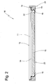
- Fig. 2 is a vertical section through the bulb 10 of Fig. 1 shown.
- the light-emitting means 10 is in Fig. 2 composed. How out Fig. 2 can be seen, closes the insulating housing 21 with the plane of the visible surface 1 from. No parts of the insulating housing 21 cover the visible surface 12th
- connection contacts 16 are materially connected to the metal plate deposited on the underside on the carrier plate 11 via the contact surface 17 of the first contact leg 18.
- the holding opening 20 of the second contact leg 19 is penetrated by a retaining pin 12 which is formed by the insulating housing 21.
- the heat sink 15 is arranged on the cover plate 14. To optimize the heat transfer from the cover plate 14 to the heat sink 15 may be provided in the region of the adjoining surfaces, a thermal paste or film.
- the heatsink 15 close lying bottom portion of the insulating housing 21 is provided with a recess 23. About this it is possible to contact another, heat-side heat sink with the heat sink 15 of the bulb 10 to further improve heat dissipation.
- Fig. 3 shows that in relation to Fig. 2 Left-sided portion of the bulb 10.
- anchoring of the terminal contact 16 in the insulating housing 21 can be seen.
- the passage of the holding opening 20 of the second contact leg 19 through the retaining pin 22 leads to a positive connection between insulating housing 21 and terminal contact 16.
- a material connection is made between the first contact leg 18 and the metallic layer of the support plate 11.
- This is done in a preferred manner by means of an ultrasonic soldering process.
- other cohesive types of connection such as welding or gluing are conceivable.
- a heat sink 15 supplemented light element in insulating material to form the light bulb 10 according to the invention is the material connection on the part of the first contact leg 18 in conjunction with the positive connection on the part of the second contact leg 19th perfectly adequate.
- the terminal contact 16 is used in addition to the electrical contact and the mechanical support. This is one of the significant advantages of the luminous means according to the invention.
- a plurality of contacts are electrically connected to the metallic layer in order to keep the distribution of the voltage and current across the surface of the carrier plate 11 provided with OLEDs uniform.
- this requires that connection contacts of the same polarity each have to be provided individually with external connection lines.
- the contacts 16 may be provided with suitable connecting elements. Conceivable here are contact training as insulation displacement contact or pressure contact or as a screwless cable clamp.
- connection contacts 16 it is possible to tap electricity from the connection contacts 16 and to use the power supply of another light source in the manner of looping through. This is particularly advantageous in combination with the electrical connection made within the insulating housing via separate connecting elements, since the voltage supply then does not have to take place via the metallic layer.
- the light element is provided by the insulating material housing 21 with a base, which considerably simplifies the handling and assembly of illuminants 10 provided with OLEDs and makes it possible to create powerful socket-mounting systems.
- connection contacts 16 can be used.
- the connection between the contact and insulating material can then be done, for example, by a frictional connection, which can be done by means of insulation displacement technology at the same time when inserting the contacts in the insulating material, the electrical contact with connecting conductors.
- Other forms of holding the bulb 10 fixing the terminal contacts 16 in the insulating housing are conceivable.
Landscapes
- Engineering & Computer Science (AREA)
- General Engineering & Computer Science (AREA)
- Physics & Mathematics (AREA)
- Optics & Photonics (AREA)
- Electroluminescent Light Sources (AREA)
- Fastening Of Light Sources Or Lamp Holders (AREA)
- Arrangement Of Elements, Cooling, Sealing, Or The Like Of Lighting Devices (AREA)
- Planar Illumination Modules (AREA)
Description
- Die Erfindung betrifft ein Leuchtmittel mit wenigstens einer organischen, Licht emittierenden Diode (OLED), die auf einem Trägermaterial aufgebracht sind, welches mit einer metallischen Schicht bedampft ist, die der Spannungsversorgung der OLED dient und hierfür mit Anschlussleitern in Verbindung steht. Ein Leuchtmittel nach dem Oberbegriff des Anspruchs 1 wird im Dokument
JP-A-2006331856 - Neben der Anwendung von anorganischen LEDs zum Ersatz herkömmlicher Leuchtmittel finden auch vermehrt LEDs Einsatz, die auf organischer Halbleitertechnik beruhen. Leuchtmittel mit organischen, Licht emittierenden Dioden (OLED) umfassen zumeist ein plattenförmiges Trägermaterial, insbesondere Glas, auf welchem die organischen Halbleiterbauteile aufgesetzt sind. Die Spannungs- und Stromversorgung übernimmt eine auf das Trägermaterial aufgedampfte Metallschicht. Rückseitig ist das Trägermaterial mit einer Abdeckung, zumeist einer weiteren Glasplatte, versehen. Die organischen Halbleiterbauteile sind so zwischen Trägermaterial und Abdeckung gelagert. Die Abdeckung lässt jedoch in Randbereichen den Zugang zur metallischen Schicht frei, so dass diese auf verschiedene Arten elektrisch kontaktiert werden kann.
- So ist es beispielsweise bekannt, elektrische Leiter mit einem speziellem, leitfähigen Kleber auf der metallischen Schicht zu fixieren, um Elektrizität einspeisen zu können. Es besteht auch die Möglichkeit, mit einem leitfähigen Elastomer eine Verbindung herzustellen. Schließlich existiert ein Verfahren, um flexible Leiterplatten an der metallischen Schicht des Trägermaterials zu befestigen.
- Die vorgenannten Möglichkeiten zur elektrischen Anbindung von Leuchtmitteln mit organischen LEDs haben ihre spezifischen Nachteile. So sind Klebeverbindungen gegenüber scherenden Beanspruchungen ausgesprochen empfindlich, weshalb solchermaßen elektrisch angebundene Leuchtmittel gewöhnlich innerhalb von Gehäusen mit separaten Anschlusskontakten angeordnet sind.
- Bei der Nutzung von elektrisch leitenden Elastomeren ist es erforderlich, eine Kompression der Elastomere herbeizuführen, weshalb auch hier das Leuchtmittel gegen ein Widerlager gepresst werden muss. Zudem sind die Übergangswiderstände vom Elastomer zum Leuchtmittel vergleichsweise hoch.
- Die Nutzung von flexiblen Leiterplatten zur elektrischen Anbindung organischer LEDs ist aufgrund der Empfindlichkeit der elektrischen Leiterplatten auch nur in bestimmten Anwendungsfällen sinnvoll.
- Der vorgenannte Stand der Technik ist beispielsweise in Herstellerrichtlinien zur Kontaktierung von OLEDs beschrieben.
- Eine Möglichkeit, OLEDs beinhaltende Leuchtmittel zu haltern, ist beispielsweise in
DE 20 2006 012 937 U1 dargestellt und ausWO 2008/074431 A1 bekannt. - Zusammenfassend besteht im Stand der Technik ein dringender Bedarf, die elektrische Kontaktierung von OLEDs beinhaltenden Leuchtmitteln wie auch deren Halterung zu verbessern.
- Aufgabe der Erfindung ist es, eine vorteilhafte elektrische Anbindung und Halterung von Leuchtmitteln auf Basis von OLEDs bereitzustellen.
- Gelöst wird die Aufgabe von einem Leuchtmittel mit den Merkmalen des Anspruchs 1, welches sich dadurch kennzeichnet, dass wenigstens ein Anschlusskontakt einerseits stoffschlüssig an zumindest der metallischen Schicht angebunden ist und andererseits unmittelbar in einem Isolierstoffgehäuse festgelegt ist.
- Der wesentliche Vorteil der Erfindung ist darin zu sehen, dass der Anschlusskontakt nicht nur der Spannungsversorgung des Leuchtmittels, sondern auch zu dessen Halterung an einem anderen Bauteil dient. Dabei ist der Kontakt unmittelbar im Isolierstoff festgelegt, welcher seinerseits beispielsweise ein Bauteil einer Leuchte darstellen kann, bevorzugt jedoch als eine Art Sockel des Leuchtmittels dient. Die bislang getrennt voneinander betrachteten und gelösten Aufgaben der elektrischen Kontaktierung und der mechanischen Halterung des Leuchtmittels werden hier in einem Bauteil vereint.
- Zur Herstellung der stoffschlüssigen Verbindung zwischen metallischer Schicht des Trägermaterials und Anschlusskontakt ist insbesondere das Ultraschall-Löten vorgesehen. Ein Schweißen oder Kleben ist jedoch ebenfalls möglich.
- Üblicherweise werden OLED-Leuchtmittel mit mehreren Anschlusskontakten pro Pol versehen, um eine gleichmäßige Spannungs- und Stromversorgung über die mit OLEDs versehene Trägerfläche sicherzustellen. Üblicherweise sind pro Pol mehrere Kontakte vorgesehen. Wenn gemäß einer bevorzugten Ausführungsform das Isolierstoffgehäuse das Leuchtmittel einbettet und so einen Sockel für das Leuchtmittel im klassischen Sinne bildet, können in einer weiteren bevorzugten Ausführungsform gleichartige Pole innerhalb des Isolierstoffgehäuses miteinander elektrisch verbunden werden. Dies hat den wesentlichen Vorteil, dass lediglich zwei der Anschlusskontakte der externen elektrischen Anbindung dienen und der ansonsten notwendige Verdrahtungsaufwand erheblich reduziert ist.
- Es ist denkbar und vorteilhaft, wenn die mit der metallischen Schicht in Verbindung stehenden Kontakte mittelbar, aber insbesondere unmittelbar von außen zugänglich im Isolierstoffgehäuse gelagert sind. So kann an den Anschlusskontakten Elektrizität zur Versorgung eines weiteren Leuchtmittels abgenommen werden.
- Die Funktion des Anschlusskontaktes als mechanisches Halteelement für das Leuchtmittel in einem Isolierstoff ermöglicht es, ein Isolierstoffgehäuse bzw. einen Sockel für das Leuchtmittel zu schaffen, der mit der Oberflächenebene der Sichtfläche des Leuchtmittels abschließt und dieses nicht überdeckt. So sind durch Aneinanderreihen mehrerer gleichartiger Leuchtmittel einheitliche Flächenleuchten herstellbar.
- Weitere Vorteile der Erfindung folgen aus der nachfolgenden Beschreibung eines Ausführungsbeispiels. Es zeigen:
- Fig. 1:
- ein erfindungsgemäßes Leuchtmittel in Explosionsdarstellung,
- Fig. 2
- das zusammengesetzte Leuchtmittel gemäß
Fig. 1 in vertikaler Schnittdarstellung, - Fig. 3:
- Eine Teilansicht des Leuchtmittels gemäß
Fig. 2 mit Blick auf einen Anschlusskontakt. - In den Figuren ist ein Leuchtmittel gemäß der Erfindung insgesamt mit der Bezugsziffer 10 versehen. Das Leuchtmittel 10 umfasst zunächst eine Trägerplatte 11 aus Glas, deren von einem Betrachter wahrzunehmenden Sichtfläche 12, die die Licht emittierende Oberfläche 13 bildet, hinsichtlich der
Fig. 1 nach oben gewandt ist. - Auf der Unterseite der Trägerplatte 11 ist zunächst eine hier nicht näher dargestellte metallische Schicht aufgedampft, die im Randbereich der Trägerplatte 11 frei zugänglich ist und der Anbindung von elektrischen Anschlüssen dient. In einem durch eine Abdeckplatte 14 überdeckten Bereich bildet die metallische Schicht Leiterbahnen zur Spannungsversorgung von auf der Trägerplatte 11 aufgebrachten, organischen, Licht emittierenden Dioden (OLED) aus. Die Abdeckplatte 14 ist auf der der Sichtfläche abgewandten Seite der Trägerplatte 11 angeordnet, so dass insbesondere die OLEDs zwischen Trägerplatte 11 und Abdeckplatte 14 liegen.
- Unterhalb der Abdeckplatte 14 ist in
Fig. 1 ein Kühlkörper 15 dargestellt, der in seinen Abmessungen in etwa der Abdeckplatte 14 entspricht und in zusammengesetztem Zustand des Leuchtmittels 10 unmittelbar an der Abdeckplatte 14 angesetzt ist. Der Kühlkörper 15 dient der Abfuhr der beim Betrieb der OLEDs entstehenden Wärme. - Dargestellt sind weiterhin elektrische Anschlusskontakte 16. Diese weisen eine zur Trägerplatte 11 gerichtete Kontaktfläche 17 auf, mit welcher sie an der im Randbereich der Trägerplatte 11 zugänglichen, metallischen Schicht angeordnet werden. Die Kontaktfläche 17 wird durch einen ersten Kontaktschenkel 18 des Anschlusskontaktes 16 gebildet. Ein zweiter Kontaktschenkel 19 des Anschlusskontaktes 16 ist in
Fig. 1 rechtwinklig zum ersten Kontaktschenkel 18 angeordnet und mit einer Halteöffnung 20 versehen. Schließlich ist inFig. 1 ein rahmenartiges Isolierstoffgehäuse 21 dargestellt, welches die vorbeschriebenen Bauteile aufnimmt. - In
Fig. 2 ist ein Vertikalschnitt durch das Leuchtmittel 10 derFig. 1 gezeigt. Das Leuchtmittel 10 ist inFig. 2 zusammengesetzt. Wie ausFig. 2 ersichtlich ist, schließt das Isolierstoffgehäuse 21 mit der Ebene der Sichtfläche 1 ab. Keine Teile des Isolierstoffgehäuses 21 bedecken die Sichtfläche 12. - Die Anschlusskontakte 16 sind stoffschlüssig mit der auf die Trägerplatte 11 unterseitig aufgedampften metallischen Schicht über die Kontaktfläche 17 des ersten Kontaktschenkels 18 verbunden. Die Halteöffnung 20 des zweiten Kontaktschenkels 19 ist von einem Haltezapfen 12 durchgriffen, der vom Isolierstoffgehäuse 21 ausgebildet ist. Der Kühlkörper 15 ist an der Abdeckplatte 14 angeordnet. Zur Optimierung des Wärmeüberganges von der Abdeckplatte 14 auf den Kühlkörper 15 kann im Bereich der aneinandergrenzenden Oberflächen eine Wärmeleitpaste oder -folie vorgesehen sein. Der dem Kühlkörper 15 naheliegende Bodenbereich des Isolierstoffgehäuses 21 ist mit einer Ausnehmung 23 versehen. Über diese ist es möglich, einen weiteren, leuchtenseitigen Kühlkörper mit dem Kühlkörper 15 des Leuchtmittels 10 zu kontaktieren, um die Wärmeabfuhr weiter zu verbessern.
-
Fig. 3 zeigt den in Bezug aufFig. 2 linksseitigen Teilabschnitt des Leuchtmittels 10. In dieser Darstellung ist noch einmal besonders gut die Verankerung des Anschlusskontaktes 16 im Isolierstoffgehäuse 21 zu entnehmen. Das Durchgreifen der Halteöffnung 20 des zweiten Kontaktschenkels 19 durch den Haltezapfen 22 führt zu einem Formschluss zwischen Isolierstoffgehäuse 21 und Anschlusskontakt 16. Zwischen dem ersten Kontaktschenkel 18 und der metallischen Schicht der Trägerplatte 11 wird ein Stoffschluss hergestellt. Dies geschieht in bevorzugter Weise mittels eines Ultraschall-Lötverfahrens. Andere stoffschlüssige Verbindungsarten wie das Schweißen oder Kleben sind jedoch denkbar. - Zur Halterung des aus Trägerplatte 11, Abdeckplatte 14 und den dazwischen gelagerten OLEDs gebildete und bei Bedarf um einen Kühlkörper 15 ergänzten Lichtelementes im Isolierstoffgehäuse zur Bildung des erfindungsgemäßen Leuchtmittels 10 ist der Stoffschluss seitens des ersten Kontaktschenkels 18 in Verbindung mit dem Formschluss seitens des zweiten Kontaktschenkels 19 vollkommen ausreichend. Insofern dient der Anschlusskontakt 16 neben der elektrischen Kontaktierung auch der mechanischen Halterung. Dies ist einer der wesentlichen Vorteile des erfindungsgemäßen Leuchtmittels.
- In der Regel werden, wie eingangs beschrieben und auch hier dargestellt, mehrere Kontakte mit der metallischen Schicht elektrisch verbunden, um die Verteilung der Spannung und Stromstärke über die mit OLEDs versehene Oberfläche der Trägerplatte 11 gleichmäßig zu halten. Im Stand der Technik bedingt dies, dass Anschlusskontakte gleicher Polarität jeweils einzeln mit externen Anschlussleitungen versehen werden müssen. Bei der Erfindung hingegen ist es möglich, die elektrische Verbindung gleichartiger Pole untereinander innerhalb des Isolierstoffgehäuses 21 vorzunehmen, so dass die externe Verdrahtung lediglich noch über zwei Kontakte erfolgen muss. Hierzu können die Kontakte 16 mit geeigneten Verbindungselementen versehen sein. Denkbar sind hier Kontaktausbildungen als Schneid-Klemmkontakt oder Andruckkontakt oder als schraubenlose Kabelklemme.
- Darüber hinaus ist es möglich, Elektrizität von den Anschlusskontakten 16 abzugreifen und zur Spannungsversorgung eines weiteren Leuchtmittels nach Art eines Durchschleifens zu nutzen. Dies ist in Kombination mit der innerhalb des Isolierstoffgehäuses erfolgten elektrischen Verbindung über gesonderte Verbindungselemente von besonderem Vorteil, da die Spannungsversorgung dann nicht über die metallische Schicht erfolgen muss.
- In der in den Figuren dargestellten Form wird das Lichtelement durch das Isolierstoffgehäuse 21 mit einem Sockel versehen, welcher die Handhabbarkeit und Montage von mit OLEDs versehenen Leuchtmitteln 10 erheblich vereinfacht und die Möglichkeit zur Schaffung leistungsfähiger Sockel-Fassungssysteme ermöglicht.
- Es ist jedoch durchaus denkbar, das lediglich im Bereich einiger Kontakte einzelne Isolierstoffgehäuse vorgesehen sind. Ebenso ist es möglich, dass das Lichtelement zwar mit Anschlusskontakten versehen ist, aber kein Isolierstoffgehäuse als unmittelbar zugehöriges Bauteil aufweist.. Es wären dann ein oder mehrere Isolierstoffgehäuse vorzusehen, beispielsweise als Leuchtenteile, in welche die Anschlusskontakte 16 einsetzbar sind. Die Verbindung zwischen Kontakt und Isolierstoffgehäuse kann dann beispielsweise auch durch einen Reibschluss erfolgen, wobei mittels Schneid-Klemmtechnik gleichzeitig beim Einsetzen der Kontakte in das Isolierstoffgehäuse die elektrische Kontaktierung mit Anschlussleitern erfolgen kann. Andere Formen einer das Leuchtmittel 10 haltenden Festlegung der Anschlusskontakte 16 im Isolierstoffgehäuse sind denkbar.
-
- 10
- Leuchtmittel
- 11
- Trägerplatte
- 12
- Sichtfläche
- 13
- Licht emittierende Oberfläche
- 14
- Abdeckplatte
- 15
- Kühlkörper
- 16
- elektrische Anschlusskontakte
- 17
- Kontaktfläche
- 18
- erster Kontaktschenkel
- 19
- zweiter Kontaktschenkel
- 20
- Halteöffnung
- 21
- Isolierstoffgehäuse
- 22
- Haltezapfen
- 23
- Ausnehmung
Claims (7)
- Leuchtmittel mit wenigstens einer organischen, Licht emittierenden Diode (OLED), die auf einem Trägermaterial aufgebracht sind, welches mit einer metallischen Schicht bedampft ist, die der Spannungsversorgung der OLED dient und hierfür mit Anschlussleitern in Verbindung steht, dadurch gekennzeichnet, dass- die metallische Schicht mehrere Pole ausbildet und mehrere Anschlusskontakte eine stoffschlüssige Verbindung mit der metallischen Schicht eingehen, wobei die Kontakte gleicher Pole untereinander innerhalb des Isolierstoffgehäuses miteinander elektrisch verbunden sind,- ein einteiliges Isolierstoffgehäuse (21) vorgesehen ist,- die Anschlusskontakte (16) unmittelbar in dem Isolierstoffgehäuse festgelegt sind,- die unmittelbare Festlegung der Anschlusskontakte (16) im Isolierstoffgehäuse (21) der Halterung des Leuchtmittels im Isolierstoffgehäuse dient.- der im Isolierstoffgehäuse festgelegte Anschlusskontakt der unmittelbaren Anbindung der Anschlussleiter dient.
- Leuchtmittel nach Anspruch 1, dadurch gekennzeichnet, dass wenigstens ein im Isolierstoffgehäuse festgelegter Anschlusskontakt zugänglich ist, um mittels einer elektrischen Verbindung ein weiteres Leuchtmittel mit Elektrizität zu Versorgen
- Leuchtmittel nach einem der vorhergehenden Ansprüche, dadurch gekennzeichnet, dass das Isolierstoffgehäuse einen Kühlkörper trägt, der die beim Betrieb der OLED entstehende Wärme abführt.
- Leuchtmittel nach einem der vorhergehenden Ansprüche, dadurch gekennzeichnet, dass der Stoffschluss zwischen dem Kontakt und der metallischen Schicht mittels Ultraschalllöten, Schweißen oder Kleben hergestellt wird.
- Leuchtmittel nach einem der vorhergehenden Ansprüche, dadurch gekennzeichnet, dass das Leuchtmittel in das Isolierstoffgehäuse eingebettet ist und das Isolierstoffgehäuse so einen Sockel ausbildet, welcher in einem im Wesentlichen form- und anschlusskomplementären Fassungsteil lagerbar ist.
- Leuchtmittel nach einem der vorhergehenden Ansprüche, dadurch gekennzeichnet, dass das Leuchtmittel ausschließlich vermittels der Verbindung zwischen Kontakt und Trägermaterial einerseits und Festlegung des Kontakt im Isolierstoffgehäuse andererseits am Isolierstoffgehäuse gehalten ist.
- Leuchtmittel nach Anspruch 5 und/oder 6, dadurch gekennzeichnet, dass das Isolierstoffgehäuse die Sichtfläche des Leuchtmittels unbedeckt lässt und insbesondere mit der Oberflächenebene der Sichtfläche abschließt.
Applications Claiming Priority (2)
| Application Number | Priority Date | Filing Date | Title |
|---|---|---|---|
| DE102011107642A DE102011107642A1 (de) | 2011-07-12 | 2011-07-12 | Leuchtmittel mit wenigstens einer organischen, Licht emittierenden Diode |
| PCT/DE2012/000684 WO2013007234A1 (de) | 2011-07-12 | 2012-07-09 | Leuchtmittel mit wenigstens einer organischen, licht emittierenden diode |
Publications (2)
| Publication Number | Publication Date |
|---|---|
| EP2732209A1 EP2732209A1 (de) | 2014-05-21 |
| EP2732209B1 true EP2732209B1 (de) | 2015-09-09 |
Family
ID=46762766
Family Applications (1)
| Application Number | Title | Priority Date | Filing Date |
|---|---|---|---|
| EP12753382.6A Active EP2732209B1 (de) | 2011-07-12 | 2012-07-09 | Leuchtmittel mit wenigstens einer organischen, licht emittierenden diode |
Country Status (5)
| Country | Link |
|---|---|
| US (1) | US20140217381A1 (de) |
| EP (1) | EP2732209B1 (de) |
| JP (1) | JP5759070B2 (de) |
| DE (1) | DE102011107642A1 (de) |
| WO (1) | WO2013007234A1 (de) |
Families Citing this family (7)
| Publication number | Priority date | Publication date | Assignee | Title |
|---|---|---|---|---|
| DE202011108565U1 (de) | 2011-12-02 | 2013-03-04 | Bjb Gmbh & Co. Kg | Lampe mit wenigstens einer organischen, lichtemmitierenden Diode |
| DE102013106688B4 (de) | 2013-06-26 | 2017-08-24 | Osram Oled Gmbh | Optoelektronisches Bauelement und Verfahren zum Herstellen eines optoelektronischen Bauelementes |
| FR3010576B1 (fr) * | 2013-09-09 | 2016-12-23 | Valeo Vision | Module lumineux comportant une diode electroluminescente organique |
| US10054295B2 (en) | 2013-11-18 | 2018-08-21 | Emdedesign Gmbh | Lamp comprising at least one OLED lighting means |
| JP6323806B2 (ja) * | 2014-06-30 | 2018-05-16 | パナソニックIpマネジメント株式会社 | 発光デバイス及び移動体 |
| DE102014116740A1 (de) | 2014-11-17 | 2016-05-19 | Emdedesign Gmbh | Leuchte umfassend wenigstens zwei OLED-Leuchtmittel |
| DE102016215576A1 (de) | 2016-08-19 | 2018-02-22 | Bayerische Motoren Werke Aktiengesellschaft | Herstellen einer Halbleiterleuchtvorrichtung mit einer LED |
Family Cites Families (20)
| Publication number | Priority date | Publication date | Assignee | Title |
|---|---|---|---|---|
| DE2346745A1 (de) * | 1972-09-20 | 1974-04-04 | Douglas Johnson | Fotografisches sicherheitslicht |
| US6819036B2 (en) * | 2002-05-28 | 2004-11-16 | Eastman Kodak Company | OLED lighting apparatus |
| JP2005345935A (ja) * | 2004-06-07 | 2005-12-15 | Nippon Seiki Co Ltd | 有機el表示器 |
| US20060012985A1 (en) * | 2004-07-15 | 2006-01-19 | Eastman Kodak Company | Flat panel lighting for enclosed space illumination |
| JP2006084977A (ja) * | 2004-09-17 | 2006-03-30 | Sony Corp | 表示装置 |
| JP4507982B2 (ja) * | 2005-05-26 | 2010-07-21 | パナソニック電工株式会社 | 照明装置 |
| US7575332B2 (en) * | 2005-06-21 | 2009-08-18 | Eastman Kodak Company | Removable flat-panel lamp and fixture |
| DE102006015437A1 (de) * | 2006-03-31 | 2007-10-04 | Merck Patent Gmbh | Leuchtfliese |
| US20080037284A1 (en) * | 2006-04-21 | 2008-02-14 | Rudisill Charles A | Lightguide tile modules and modular lighting system |
| DE202006012937U1 (de) | 2006-08-23 | 2007-12-27 | LÖRSCH, Johannes | Haltevorrichtung für zu untersuchende Proben, insbesondere chemische oder biologische Substanzen o.dgl. |
| DE102006054584A1 (de) * | 2006-09-29 | 2008-04-10 | Osram Opto Semiconductors Gmbh | Ablagemöbel |
| DE202006019239U1 (de) | 2006-12-19 | 2008-04-30 | Bender & Wirth Gmbh & Co. | Vorrichtung für Leuchtmittel |
| CN101459162B (zh) * | 2007-12-11 | 2010-12-08 | 富士迈半导体精密工业(上海)有限公司 | 固态发光器件 |
| JP5336071B2 (ja) * | 2007-12-21 | 2013-11-06 | ローム株式会社 | 有機発光装置 |
| WO2010030072A2 (ko) * | 2008-09-09 | 2010-03-18 | Yang Jinho | 인터넷상의 결제 수단 제공 방법 및 제공 시스템 |
| US8444292B2 (en) * | 2008-10-24 | 2013-05-21 | Ilumisys, Inc. | End cap substitute for LED-based tube replacement light |
| JP5451104B2 (ja) * | 2009-02-20 | 2014-03-26 | パナソニック株式会社 | 照明用有機elパネル |
| DE102009046755A1 (de) * | 2009-11-17 | 2011-05-26 | Fraunhofer-Gesellschaft zur Förderung der angewandten Forschung e.V. | Organisches photoelektrisches Bauelement |
| KR101034121B1 (ko) * | 2009-12-22 | 2011-05-13 | 엘지이노텍 주식회사 | 백라이트 유닛 |
| KR101253199B1 (ko) * | 2011-07-25 | 2013-04-10 | 엘지전자 주식회사 | 조명 장치 |
-
2011
- 2011-07-12 DE DE102011107642A patent/DE102011107642A1/de not_active Withdrawn
-
2012
- 2012-07-09 WO PCT/DE2012/000684 patent/WO2013007234A1/de not_active Ceased
- 2012-07-09 EP EP12753382.6A patent/EP2732209B1/de active Active
- 2012-07-09 JP JP2014519419A patent/JP5759070B2/ja active Active
-
2014
- 2014-01-11 US US14/153,013 patent/US20140217381A1/en not_active Abandoned
Also Published As
| Publication number | Publication date |
|---|---|
| JP5759070B2 (ja) | 2015-08-05 |
| EP2732209A1 (de) | 2014-05-21 |
| US20140217381A1 (en) | 2014-08-07 |
| DE102011107642A1 (de) | 2013-01-17 |
| WO2013007234A1 (de) | 2013-01-17 |
| JP2014525125A (ja) | 2014-09-25 |
Similar Documents
| Publication | Publication Date | Title |
|---|---|---|
| EP2732209B1 (de) | Leuchtmittel mit wenigstens einer organischen, licht emittierenden diode | |
| DE102011005047B3 (de) | Leuchtvorrichtung | |
| EP1255299B1 (de) | Leistungshalbleitermodul in Druckkontaktierung | |
| DE102009001405A1 (de) | Montageanordnung eines Leuchtkörpers | |
| DE102013113001B4 (de) | Modul und Anordnung mit einem Modul | |
| DE102006048230A1 (de) | Leuchtdiodensystem, Verfahren zur Herstellung eines solchen und Hinterleuchtungseinrichtung | |
| DE102007042978A1 (de) | Lampe | |
| DE102013225411A1 (de) | Verbinder für eine LED-Modulplatine | |
| DE102010029227A1 (de) | Leuchtvorrichtung | |
| EP2347639A1 (de) | Beleuchtungsvorrichtung mit zwei leiterplatten | |
| EP2613079A1 (de) | LED-Leuchtmittel | |
| WO2015007904A1 (de) | Leuchtvorrichtung mit halbleiterlichtquelle und treiberplatine | |
| DE102012218538A1 (de) | Verfahren zur Herstellung einer Lichterzeugungseinheit | |
| DE102008039071A1 (de) | Beleuchtungsvorrichtung für Fahrzeuge | |
| AT501081B1 (de) | Led sowie led-lichtquelle | |
| DE102015111248A1 (de) | LED-Birne | |
| DE202016101292U1 (de) | Leistungshalbleitereinrichtung | |
| WO2016020446A2 (de) | Leuchtdioden-halter sowie led-lampe oder leuchte zur beleuchtung | |
| WO2019219637A1 (de) | Leiterplattenaufbau zur aufnahme wenigstens eines halbleiterleuchtmittels | |
| EP2852791B1 (de) | Leuchtvorrichtung mit treiber | |
| AT513328B1 (de) | Beleuchtungsvorrichtung | |
| WO2014026876A1 (de) | Leuchtmodul und abdeckung davon | |
| AT518330A2 (de) | Leuchte | |
| WO2017032613A1 (de) | Lichtemittierendes bauelement | |
| DE102010000035B4 (de) | Verfahren zur Herstellung einer Elektronikbaugruppe und eine nach dem Verfahren hergestellte Elektronikbaugruppe |
Legal Events
| Date | Code | Title | Description |
|---|---|---|---|
| PUAI | Public reference made under article 153(3) epc to a published international application that has entered the european phase |
Free format text: ORIGINAL CODE: 0009012 |
|
| 17P | Request for examination filed |
Effective date: 20131220 |
|
| AK | Designated contracting states |
Kind code of ref document: A1 Designated state(s): AL AT BE BG CH CY CZ DE DK EE ES FI FR GB GR HR HU IE IS IT LI LT LU LV MC MK MT NL NO PL PT RO RS SE SI SK SM TR |
|
| DAX | Request for extension of the european patent (deleted) | ||
| GRAP | Despatch of communication of intention to grant a patent |
Free format text: ORIGINAL CODE: EPIDOSNIGR1 |
|
| INTG | Intention to grant announced |
Effective date: 20150309 |
|
| GRAS | Grant fee paid |
Free format text: ORIGINAL CODE: EPIDOSNIGR3 |
|
| GRAA | (expected) grant |
Free format text: ORIGINAL CODE: 0009210 |
|
| AK | Designated contracting states |
Kind code of ref document: B1 Designated state(s): AL AT BE BG CH CY CZ DE DK EE ES FI FR GB GR HR HU IE IS IT LI LT LU LV MC MK MT NL NO PL PT RO RS SE SI SK SM TR |
|
| REG | Reference to a national code |
Ref country code: GB Ref legal event code: FG4D Free format text: NOT ENGLISH |
|
| REG | Reference to a national code |
Ref country code: AT Ref legal event code: REF Ref document number: 748439 Country of ref document: AT Kind code of ref document: T Effective date: 20150915 Ref country code: CH Ref legal event code: EP |
|
| REG | Reference to a national code |
Ref country code: IE Ref legal event code: FG4D Free format text: LANGUAGE OF EP DOCUMENT: GERMAN |
|
| REG | Reference to a national code |
Ref country code: DE Ref legal event code: R096 Ref document number: 502012004497 Country of ref document: DE |
|
| REG | Reference to a national code |
Ref country code: NL Ref legal event code: MP Effective date: 20150909 |
|
| PG25 | Lapsed in a contracting state [announced via postgrant information from national office to epo] |
Ref country code: LT Free format text: LAPSE BECAUSE OF FAILURE TO SUBMIT A TRANSLATION OF THE DESCRIPTION OR TO PAY THE FEE WITHIN THE PRESCRIBED TIME-LIMIT Effective date: 20150909 Ref country code: FI Free format text: LAPSE BECAUSE OF FAILURE TO SUBMIT A TRANSLATION OF THE DESCRIPTION OR TO PAY THE FEE WITHIN THE PRESCRIBED TIME-LIMIT Effective date: 20150909 Ref country code: NO Free format text: LAPSE BECAUSE OF FAILURE TO SUBMIT A TRANSLATION OF THE DESCRIPTION OR TO PAY THE FEE WITHIN THE PRESCRIBED TIME-LIMIT Effective date: 20151209 Ref country code: LV Free format text: LAPSE BECAUSE OF FAILURE TO SUBMIT A TRANSLATION OF THE DESCRIPTION OR TO PAY THE FEE WITHIN THE PRESCRIBED TIME-LIMIT Effective date: 20150909 Ref country code: GR Free format text: LAPSE BECAUSE OF FAILURE TO SUBMIT A TRANSLATION OF THE DESCRIPTION OR TO PAY THE FEE WITHIN THE PRESCRIBED TIME-LIMIT Effective date: 20151210 |
|
| REG | Reference to a national code |
Ref country code: LT Ref legal event code: MG4D |
|
| PG25 | Lapsed in a contracting state [announced via postgrant information from national office to epo] |
Ref country code: ES Free format text: LAPSE BECAUSE OF FAILURE TO SUBMIT A TRANSLATION OF THE DESCRIPTION OR TO PAY THE FEE WITHIN THE PRESCRIBED TIME-LIMIT Effective date: 20150909 Ref country code: HR Free format text: LAPSE BECAUSE OF FAILURE TO SUBMIT A TRANSLATION OF THE DESCRIPTION OR TO PAY THE FEE WITHIN THE PRESCRIBED TIME-LIMIT Effective date: 20150909 Ref country code: RS Free format text: LAPSE BECAUSE OF FAILURE TO SUBMIT A TRANSLATION OF THE DESCRIPTION OR TO PAY THE FEE WITHIN THE PRESCRIBED TIME-LIMIT Effective date: 20150909 Ref country code: SE Free format text: LAPSE BECAUSE OF FAILURE TO SUBMIT A TRANSLATION OF THE DESCRIPTION OR TO PAY THE FEE WITHIN THE PRESCRIBED TIME-LIMIT Effective date: 20150909 |
|
| PG25 | Lapsed in a contracting state [announced via postgrant information from national office to epo] |
Ref country code: NL Free format text: LAPSE BECAUSE OF FAILURE TO SUBMIT A TRANSLATION OF THE DESCRIPTION OR TO PAY THE FEE WITHIN THE PRESCRIBED TIME-LIMIT Effective date: 20150909 |
|
| PG25 | Lapsed in a contracting state [announced via postgrant information from national office to epo] |
Ref country code: EE Free format text: LAPSE BECAUSE OF FAILURE TO SUBMIT A TRANSLATION OF THE DESCRIPTION OR TO PAY THE FEE WITHIN THE PRESCRIBED TIME-LIMIT Effective date: 20150909 Ref country code: SK Free format text: LAPSE BECAUSE OF FAILURE TO SUBMIT A TRANSLATION OF THE DESCRIPTION OR TO PAY THE FEE WITHIN THE PRESCRIBED TIME-LIMIT Effective date: 20150909 Ref country code: CZ Free format text: LAPSE BECAUSE OF FAILURE TO SUBMIT A TRANSLATION OF THE DESCRIPTION OR TO PAY THE FEE WITHIN THE PRESCRIBED TIME-LIMIT Effective date: 20150909 Ref country code: IS Free format text: LAPSE BECAUSE OF FAILURE TO SUBMIT A TRANSLATION OF THE DESCRIPTION OR TO PAY THE FEE WITHIN THE PRESCRIBED TIME-LIMIT Effective date: 20160109 Ref country code: IT Free format text: LAPSE BECAUSE OF FAILURE TO SUBMIT A TRANSLATION OF THE DESCRIPTION OR TO PAY THE FEE WITHIN THE PRESCRIBED TIME-LIMIT Effective date: 20150909 |
|
| PG25 | Lapsed in a contracting state [announced via postgrant information from national office to epo] |
Ref country code: RO Free format text: LAPSE BECAUSE OF FAILURE TO SUBMIT A TRANSLATION OF THE DESCRIPTION OR TO PAY THE FEE WITHIN THE PRESCRIBED TIME-LIMIT Effective date: 20150909 Ref country code: PL Free format text: LAPSE BECAUSE OF FAILURE TO SUBMIT A TRANSLATION OF THE DESCRIPTION OR TO PAY THE FEE WITHIN THE PRESCRIBED TIME-LIMIT Effective date: 20150909 Ref country code: PT Free format text: LAPSE BECAUSE OF FAILURE TO SUBMIT A TRANSLATION OF THE DESCRIPTION OR TO PAY THE FEE WITHIN THE PRESCRIBED TIME-LIMIT Effective date: 20160111 |
|
| REG | Reference to a national code |
Ref country code: DE Ref legal event code: R097 Ref document number: 502012004497 Country of ref document: DE |
|
| PLBE | No opposition filed within time limit |
Free format text: ORIGINAL CODE: 0009261 |
|
| STAA | Information on the status of an ep patent application or granted ep patent |
Free format text: STATUS: NO OPPOSITION FILED WITHIN TIME LIMIT |
|
| 26N | No opposition filed |
Effective date: 20160610 |
|
| PG25 | Lapsed in a contracting state [announced via postgrant information from national office to epo] |
Ref country code: DK Free format text: LAPSE BECAUSE OF FAILURE TO SUBMIT A TRANSLATION OF THE DESCRIPTION OR TO PAY THE FEE WITHIN THE PRESCRIBED TIME-LIMIT Effective date: 20150909 Ref country code: SI Free format text: LAPSE BECAUSE OF FAILURE TO SUBMIT A TRANSLATION OF THE DESCRIPTION OR TO PAY THE FEE WITHIN THE PRESCRIBED TIME-LIMIT Effective date: 20150909 |
|
| PG25 | Lapsed in a contracting state [announced via postgrant information from national office to epo] |
Ref country code: BE Free format text: LAPSE BECAUSE OF NON-PAYMENT OF DUE FEES Effective date: 20160731 |
|
| REG | Reference to a national code |
Ref country code: CH Ref legal event code: PL |
|
| GBPC | Gb: european patent ceased through non-payment of renewal fee |
Effective date: 20160709 |
|
| PG25 | Lapsed in a contracting state [announced via postgrant information from national office to epo] |
Ref country code: MC Free format text: LAPSE BECAUSE OF FAILURE TO SUBMIT A TRANSLATION OF THE DESCRIPTION OR TO PAY THE FEE WITHIN THE PRESCRIBED TIME-LIMIT Effective date: 20150909 |
|
| PG25 | Lapsed in a contracting state [announced via postgrant information from national office to epo] |
Ref country code: CH Free format text: LAPSE BECAUSE OF NON-PAYMENT OF DUE FEES Effective date: 20160731 Ref country code: FR Free format text: LAPSE BECAUSE OF NON-PAYMENT OF DUE FEES Effective date: 20160801 Ref country code: LI Free format text: LAPSE BECAUSE OF NON-PAYMENT OF DUE FEES Effective date: 20160731 |
|
| REG | Reference to a national code |
Ref country code: FR Ref legal event code: ST Effective date: 20170331 |
|
| REG | Reference to a national code |
Ref country code: IE Ref legal event code: MM4A |
|
| PG25 | Lapsed in a contracting state [announced via postgrant information from national office to epo] |
Ref country code: GB Free format text: LAPSE BECAUSE OF NON-PAYMENT OF DUE FEES Effective date: 20160709 |
|
| PG25 | Lapsed in a contracting state [announced via postgrant information from national office to epo] |
Ref country code: IE Free format text: LAPSE BECAUSE OF NON-PAYMENT OF DUE FEES Effective date: 20160709 |
|
| PG25 | Lapsed in a contracting state [announced via postgrant information from national office to epo] |
Ref country code: LU Free format text: LAPSE BECAUSE OF NON-PAYMENT OF DUE FEES Effective date: 20160709 |
|
| PG25 | Lapsed in a contracting state [announced via postgrant information from national office to epo] |
Ref country code: HU Free format text: LAPSE BECAUSE OF FAILURE TO SUBMIT A TRANSLATION OF THE DESCRIPTION OR TO PAY THE FEE WITHIN THE PRESCRIBED TIME-LIMIT; INVALID AB INITIO Effective date: 20120709 Ref country code: SM Free format text: LAPSE BECAUSE OF FAILURE TO SUBMIT A TRANSLATION OF THE DESCRIPTION OR TO PAY THE FEE WITHIN THE PRESCRIBED TIME-LIMIT Effective date: 20150909 Ref country code: CY Free format text: LAPSE BECAUSE OF FAILURE TO SUBMIT A TRANSLATION OF THE DESCRIPTION OR TO PAY THE FEE WITHIN THE PRESCRIBED TIME-LIMIT Effective date: 20150909 |
|
| PG25 | Lapsed in a contracting state [announced via postgrant information from national office to epo] |
Ref country code: MK Free format text: LAPSE BECAUSE OF FAILURE TO SUBMIT A TRANSLATION OF THE DESCRIPTION OR TO PAY THE FEE WITHIN THE PRESCRIBED TIME-LIMIT Effective date: 20150909 Ref country code: MT Free format text: LAPSE BECAUSE OF FAILURE TO SUBMIT A TRANSLATION OF THE DESCRIPTION OR TO PAY THE FEE WITHIN THE PRESCRIBED TIME-LIMIT Effective date: 20150909 |
|
| PG25 | Lapsed in a contracting state [announced via postgrant information from national office to epo] |
Ref country code: BG Free format text: LAPSE BECAUSE OF FAILURE TO SUBMIT A TRANSLATION OF THE DESCRIPTION OR TO PAY THE FEE WITHIN THE PRESCRIBED TIME-LIMIT Effective date: 20150909 |
|
| REG | Reference to a national code |
Ref country code: AT Ref legal event code: MM01 Ref document number: 748439 Country of ref document: AT Kind code of ref document: T Effective date: 20170709 |
|
| PG25 | Lapsed in a contracting state [announced via postgrant information from national office to epo] |
Ref country code: TR Free format text: LAPSE BECAUSE OF FAILURE TO SUBMIT A TRANSLATION OF THE DESCRIPTION OR TO PAY THE FEE WITHIN THE PRESCRIBED TIME-LIMIT Effective date: 20150909 Ref country code: AL Free format text: LAPSE BECAUSE OF FAILURE TO SUBMIT A TRANSLATION OF THE DESCRIPTION OR TO PAY THE FEE WITHIN THE PRESCRIBED TIME-LIMIT Effective date: 20150909 |
|
| PG25 | Lapsed in a contracting state [announced via postgrant information from national office to epo] |
Ref country code: AT Free format text: LAPSE BECAUSE OF NON-PAYMENT OF DUE FEES Effective date: 20170709 |
|
| P01 | Opt-out of the competence of the unified patent court (upc) registered |
Effective date: 20230518 |
|
| PGFP | Annual fee paid to national office [announced via postgrant information from national office to epo] |
Ref country code: DE Payment date: 20250527 Year of fee payment: 14 |