EP2731410A1 - Opto-electric hybrid board - Google Patents
Opto-electric hybrid board Download PDFInfo
- Publication number
- EP2731410A1 EP2731410A1 EP13179698.9A EP13179698A EP2731410A1 EP 2731410 A1 EP2731410 A1 EP 2731410A1 EP 13179698 A EP13179698 A EP 13179698A EP 2731410 A1 EP2731410 A1 EP 2731410A1
- Authority
- EP
- European Patent Office
- Prior art keywords
- opto
- electric hybrid
- hybrid board
- optical waveguide
- layer
- Prior art date
- Legal status (The legal status is an assumption and is not a legal conclusion. Google has not performed a legal analysis and makes no representation as to the accuracy of the status listed.)
- Withdrawn
Links
- 230000003287 optical effect Effects 0.000 claims abstract description 47
- 238000005253 cladding Methods 0.000 claims abstract description 40
- 238000000034 method Methods 0.000 description 15
- 230000015572 biosynthetic process Effects 0.000 description 8
- 239000000463 material Substances 0.000 description 8
- 230000000052 comparative effect Effects 0.000 description 7
- 239000000654 additive Substances 0.000 description 5
- 230000005540 biological transmission Effects 0.000 description 5
- 239000003822 epoxy resin Substances 0.000 description 5
- 229920000647 polyepoxide Polymers 0.000 description 5
- 239000011347 resin Substances 0.000 description 5
- 229920005989 resin Polymers 0.000 description 5
- RYGMFSIKBFXOCR-UHFFFAOYSA-N Copper Chemical compound [Cu] RYGMFSIKBFXOCR-UHFFFAOYSA-N 0.000 description 4
- 229910052802 copper Inorganic materials 0.000 description 4
- 239000010949 copper Substances 0.000 description 4
- 230000000694 effects Effects 0.000 description 4
- 229920001721 polyimide Polymers 0.000 description 4
- 239000000758 substrate Substances 0.000 description 4
- HEMHJVSKTPXQMS-UHFFFAOYSA-M Sodium hydroxide Chemical compound [OH-].[Na+] HEMHJVSKTPXQMS-UHFFFAOYSA-M 0.000 description 3
- 239000004642 Polyimide Substances 0.000 description 2
- 230000000996 additive effect Effects 0.000 description 2
- 238000005452 bending Methods 0.000 description 2
- 238000009713 electroplating Methods 0.000 description 2
- 238000004519 manufacturing process Methods 0.000 description 2
- 229910052751 metal Inorganic materials 0.000 description 2
- 239000002184 metal Substances 0.000 description 2
- VYZAMTAEIAYCRO-UHFFFAOYSA-N Chromium Chemical compound [Cr] VYZAMTAEIAYCRO-UHFFFAOYSA-N 0.000 description 1
- 229910052804 chromium Inorganic materials 0.000 description 1
- 239000011651 chromium Substances 0.000 description 1
- 230000003247 decreasing effect Effects 0.000 description 1
- 238000007772 electroless plating Methods 0.000 description 1
- 238000005530 etching Methods 0.000 description 1
- 238000012986 modification Methods 0.000 description 1
- 230000004048 modification Effects 0.000 description 1
- 239000009719 polyimide resin Substances 0.000 description 1
- 238000005549 size reduction Methods 0.000 description 1
- 238000004544 sputter deposition Methods 0.000 description 1
Images


Classifications
-
- G—PHYSICS
- G02—OPTICS
- G02B—OPTICAL ELEMENTS, SYSTEMS OR APPARATUS
- G02B6/00—Light guides; Structural details of arrangements comprising light guides and other optical elements, e.g. couplings
- G02B6/10—Light guides; Structural details of arrangements comprising light guides and other optical elements, e.g. couplings of the optical waveguide type
- G02B6/12—Light guides; Structural details of arrangements comprising light guides and other optical elements, e.g. couplings of the optical waveguide type of the integrated circuit kind
- G02B6/12002—Three-dimensional structures
-
- G—PHYSICS
- G02—OPTICS
- G02B—OPTICAL ELEMENTS, SYSTEMS OR APPARATUS
- G02B6/00—Light guides; Structural details of arrangements comprising light guides and other optical elements, e.g. couplings
- G02B6/10—Light guides; Structural details of arrangements comprising light guides and other optical elements, e.g. couplings of the optical waveguide type
- G02B6/12—Light guides; Structural details of arrangements comprising light guides and other optical elements, e.g. couplings of the optical waveguide type of the integrated circuit kind
- G02B6/13—Integrated optical circuits characterised by the manufacturing method
- G02B6/138—Integrated optical circuits characterised by the manufacturing method by using polymerisation
-
- G—PHYSICS
- G02—OPTICS
- G02B—OPTICAL ELEMENTS, SYSTEMS OR APPARATUS
- G02B6/00—Light guides; Structural details of arrangements comprising light guides and other optical elements, e.g. couplings
- G02B6/10—Light guides; Structural details of arrangements comprising light guides and other optical elements, e.g. couplings of the optical waveguide type
- G02B6/12—Light guides; Structural details of arrangements comprising light guides and other optical elements, e.g. couplings of the optical waveguide type of the integrated circuit kind
-
- G—PHYSICS
- G02—OPTICS
- G02B—OPTICAL ELEMENTS, SYSTEMS OR APPARATUS
- G02B6/00—Light guides; Structural details of arrangements comprising light guides and other optical elements, e.g. couplings
- G02B6/10—Light guides; Structural details of arrangements comprising light guides and other optical elements, e.g. couplings of the optical waveguide type
-
- H—ELECTRICITY
- H05—ELECTRIC TECHNIQUES NOT OTHERWISE PROVIDED FOR
- H05K—PRINTED CIRCUITS; CASINGS OR CONSTRUCTIONAL DETAILS OF ELECTRIC APPARATUS; MANUFACTURE OF ASSEMBLAGES OF ELECTRICAL COMPONENTS
- H05K1/00—Printed circuits
- H05K1/02—Details
-
- H—ELECTRICITY
- H05—ELECTRIC TECHNIQUES NOT OTHERWISE PROVIDED FOR
- H05K—PRINTED CIRCUITS; CASINGS OR CONSTRUCTIONAL DETAILS OF ELECTRIC APPARATUS; MANUFACTURE OF ASSEMBLAGES OF ELECTRICAL COMPONENTS
- H05K1/00—Printed circuits
- H05K1/02—Details
- H05K1/0274—Optical details, e.g. printed circuits comprising integral optical means
-
- H—ELECTRICITY
- H05—ELECTRIC TECHNIQUES NOT OTHERWISE PROVIDED FOR
- H05K—PRINTED CIRCUITS; CASINGS OR CONSTRUCTIONAL DETAILS OF ELECTRIC APPARATUS; MANUFACTURE OF ASSEMBLAGES OF ELECTRICAL COMPONENTS
- H05K1/00—Printed circuits
- H05K1/02—Details
- H05K1/0277—Bendability or stretchability details
- H05K1/028—Bending or folding regions of flexible printed circuits
-
- H—ELECTRICITY
- H05—ELECTRIC TECHNIQUES NOT OTHERWISE PROVIDED FOR
- H05K—PRINTED CIRCUITS; CASINGS OR CONSTRUCTIONAL DETAILS OF ELECTRIC APPARATUS; MANUFACTURE OF ASSEMBLAGES OF ELECTRICAL COMPONENTS
- H05K2201/00—Indexing scheme relating to printed circuits covered by H05K1/00
- H05K2201/09—Shape and layout
- H05K2201/09209—Shape and layout details of conductors
- H05K2201/09218—Conductive traces
- H05K2201/09236—Parallel layout
-
- H—ELECTRICITY
- H05—ELECTRIC TECHNIQUES NOT OTHERWISE PROVIDED FOR
- H05K—PRINTED CIRCUITS; CASINGS OR CONSTRUCTIONAL DETAILS OF ELECTRIC APPARATUS; MANUFACTURE OF ASSEMBLAGES OF ELECTRICAL COMPONENTS
- H05K2201/00—Indexing scheme relating to printed circuits covered by H05K1/00
- H05K2201/09—Shape and layout
- H05K2201/09818—Shape or layout details not covered by a single group of H05K2201/09009 - H05K2201/09809
- H05K2201/09909—Special local insulating pattern, e.g. as dam around component
-
- H—ELECTRICITY
- H05—ELECTRIC TECHNIQUES NOT OTHERWISE PROVIDED FOR
- H05K—PRINTED CIRCUITS; CASINGS OR CONSTRUCTIONAL DETAILS OF ELECTRIC APPARATUS; MANUFACTURE OF ASSEMBLAGES OF ELECTRICAL COMPONENTS
- H05K2201/00—Indexing scheme relating to printed circuits covered by H05K1/00
- H05K2201/09—Shape and layout
- H05K2201/09818—Shape or layout details not covered by a single group of H05K2201/09009 - H05K2201/09809
- H05K2201/09972—Partitioned, e.g. portions of a PCB dedicated to different functions; Boundary lines therefore; Portions of a PCB being processed separately or differently
-
- H—ELECTRICITY
- H05—ELECTRIC TECHNIQUES NOT OTHERWISE PROVIDED FOR
- H05K—PRINTED CIRCUITS; CASINGS OR CONSTRUCTIONAL DETAILS OF ELECTRIC APPARATUS; MANUFACTURE OF ASSEMBLAGES OF ELECTRICAL COMPONENTS
- H05K2203/00—Indexing scheme relating to apparatus or processes for manufacturing printed circuits covered by H05K3/00
- H05K2203/15—Position of the PCB during processing
- H05K2203/1572—Processing both sides of a PCB by the same process; Providing a similar arrangement of components on both sides; Making interlayer connections from two sides
Definitions
- the present invention relates to an opto-electric hybrid board including an electric circuit board and an optical waveguide which are stacked together.
- This opto-electric hybrid board includes: an electric circuit board E 0 including an insulative flexible substrate (insulative layer) 51, electrical interconnect lines 52 formed on the front surface of the flexible substrate 51, and an insulative coverlay (interconnect line cover layer) 53 formed on the front surface of the flexible substrate 51 and for covering and protecting the electrical interconnect lines 52; and an optical waveguide (an optical interconnect line) W 0 (including an under cladding layer 56, cores 57 and an over cladding layer 58) made of epoxy resin and the like and stacked on the back surface (a surface opposite from the surface with the electrical interconnect lines 52 formed thereon) of the flexible substrate 51 of the electric circuit board E 0 .
- an electric circuit board E 0 including an insulative flexible substrate (insulative layer) 51, electrical interconnect lines 52 formed on the front surface of the flexible substrate 51, and an insulative coverlay (interconnect line cover layer) 53 formed on the front surface of the flexible substrate 51 and for covering and protecting the electrical interconnect lines 52; and an optical waveguide (an optical inter
- Both of the electric circuit board E 0 and the optical waveguide W 0 in the opto-electric hybrid board are thin and accordingly flexible.
- the opto-electric hybrid board has been used in a small space when in a bent position, and used in a movable section such as a hinge.
- the coverlay 53 which covers and protects the electrical interconnect lines 52 and the optical waveguide W 0 are in general disposed in stacked relation (in vertically stacked relation as seen in FIG. 7 ).
- the thickness of the aforementioned opto-electric hybrid board is the sum of the thickness of the electric circuit board E 0 and the thickness of the optical waveguide W 0 .
- An opto-electric hybrid board is provided which is capable of significantly reducing stresses applied to a bent portion thereof.
- the interconnect line cover layer and the optical waveguide are disposed in non-overlapping relation.
- the thickness of the to-be-bent portion of the opto-electric hybrid board is less than the sum of the thickness of the electric circuit board and the thickness of the optical waveguide.
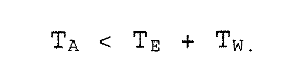
- T A which is the thickness of a bent portion of the opto-electric hybrid board when in a bent position to T E which is the thickness of the electric circuit board and T w which is the thickness of the optical waveguide satisfies the following condition (1).
- stresses applied to the bent portion are significantly reduced. Breaks and cracks are prevented from occurring in the bent portion. This achieves proper information transmission.
- FIG. 1 is a perspective view schematically showing an opto-electric hybrid board according to a first preferred embodiment.
- the opto-electric hybrid board according to the first preferred embodiment is strip-shaped, and includes an electric circuit board E and an optical waveguide W.
- electrical interconnect lines 2 and insulative coverlays (interconnect line cover layers) 3 for covering and protecting the electrical interconnect lines 2 are formed on the front surface side (top as seen in FIG. 1 ) of laterally opposite side portions of the opto-electric hybrid board and extend in the longitudinal direction of the opto-electric hybrid board.
- the optical waveguide W is formed on the back surface side (bottom as seen in FIG. 1 ) of a laterally middle portion of the opto-electric hybrid board.
- the coverlays 3 and the optical waveguide W are disposed in non-overlapping relation throughout the longitudinal direction of the strip-shaped opto-electric hybrid board.
- the electric circuit board E includes a strip-shaped insulative layer 1, the electrical interconnect lines 2 formed on the front surface of laterally opposite side portions of the insulative layer 1 and extending in the longitudinal direction thereof, and the coverlays 3 formed on the front surface of the laterally opposite side portions of the insulative layer 1 and for providing insulative protection to the electrical interconnect lines 2.
- the optical waveguide W includes a first cladding layer (under cladding layer) 6, cores 7 formed in a predetermined pattern on the front surface of the first cladding layer 6, and a second cladding layer (over cladding layer) 8 formed on the front surface of the first cladding layer 6 so as to cover the cores 7.
- the first cladding layer 6 has a back surface (a surface opposite from the surface with the cores 7 formed thereon) in contact with the insulative layer 1 of the electric circuit board E.
- the electrical interconnect lines 2 are formed on the front surface of the laterally opposite side portions of the insulative layer 1 by a semi-additive process, for example.
- the semi-additive process is as follows. First, a metal film (not shown) made of copper, chromium and the like is formed on the front surface of the insulative layer 1 by sputtering, electroless plating or the like. This metal film serves as a seed layer (a layer serving as a basis material for the formation of an electroplated layer) for a subsequent electroplating process. Then, a photosensitive resist (not shown) is laminated to the opposite surfaces of a laminate comprised of the insulative layer 1 and the seed layer.
- a photolithographic process is performed to form holes having the pattern of the electrical interconnect lines 2 in the photosensitive resist on the side where the seed layer is formed, so that surface portions of the seed layer are uncovered at the bottoms of the holes.
- electroplating is performed to form an electroplated layer made of copper and the like in a stacked manner on the surface portions of the seed layer uncovered at the bottoms of the holes.
- the photosensitive resist is stripped away using an aqueous sodium hydroxide solution and the like.
- a portion of the seed layer on which the electroplated layer is not formed is removed by soft etching. Laminate portions comprised of the remaining seed layer and the electroplated layer are the electrical interconnect lines 2.
- the electrical interconnect lines 2 are preferably thin, and preferably have a thickness of not greater than 100 ⁇ m, more preferably not greater than 20 ⁇ m. It should be noted that the electrical interconnect lines 2 may be formed by an additive process, a subtractive process and the like in addition to the semi-additive process.
- a photosensitive insulating resin including a polyimide resin and the like is applied onto the electrical interconnect lines 2 to thereby form the coverlays 3 by a photolithographic process.
- the coverlays 3 are preferably thinner, and preferably have a thickness (as measured from the front surface of the insulative layer 1) of not greater than 200 ⁇ , more preferably not greater than 50 ⁇ m. In this manner, the electric circuit board E is formed.
- a photosensitive resin such as a photosensitive epoxy resin which is a material for the formation of the first cladding layer (under cladding layer) 6 is applied to the back surface of the insulative layer 1, as shown in FIG. 2C . Thereafter, a laterally middle portion of the applied layer is exposed to irradiation light. This exposure cures the laterally middle portion of the applied layer to form the first cladding layer 6.
- the first cladding layer 6 is preferably thin, and preferably has a thickness of not greater than 80 ⁇ m, more preferably not greater than 40 ⁇ m. It should be noted that the back surface of the insulative layer 1 is positioned to face upward when the optical waveguide W is formed (when the aforementioned first cladding layer 6, the cores 7 to be described later and the second cladding layer (over cladding layer) 8 to be described later are formed) .
- the cores 7 having a predetermined pattern are formed on the front surface (the lower surface as seen in the figure) of the first cladding layer 6 by a photolithographic process.
- the cores 7 are preferably thick, and preferably have a thickness of not less than 5 ⁇ m, more preferably not less than 20 ⁇ m.
- the cores 7 are preferably thin, and preferably have a thickness of not greater than 400 ⁇ m, more preferably not greater than 100 ⁇ m.
- An example of a material for the formation of the cores 7 includes a photosensitive resin similar to that for the first cladding layer 6, and the material used herein has a refractive index higher than that of the material for the formation of the aforementioned first cladding layer 6 and the second cladding layer 8 to be described below (with reference to FIG. 2E ), with the cores 7 formed.
- the adjustment of the refractive index may be made, for example, by adjusting the selection of the types of the materials for the formation of the first cladding layer 6, the cores 7 and the second cladding layer 8, and the composition ratio thereof.
- the second cladding layer 8 is formed on the front surface (the lower surface as seen in the figure) of the first cladding layer 6 by a photolithographic process so as to cover the cores 7.
- the second cladding layer 8 is preferably thin, and preferably has a thickness (as measured from the cores 7) of not greater than 200 ⁇ m, more preferably not greater than 100 ⁇ m.
- An example of the material for the formation of the second cladding layer 8 includes a photosensitive resin similar to that for the first cladding layer 6. In this manner, the optical waveguide W is formed on the back surface of the insulative layer 1. This provides an intended opto-electric hybrid board.
- FIG. 3 is a front view schematically showing an opto-electric hybrid board according to a second preferred embodiment.
- the electrical interconnect lines 2 and a coverlay 3 are formed on the front surface side (top as seen in FIG. 3 ) of one of the laterally opposite side portions (a left-hand portion as seen in FIG. 3 ) of the opto-electric hybrid board, and the optical waveguide W is formed on the back surface side (bottom as seen in FIG. 3 ) of the other of the laterally opposite side portions (a right-hand portion as seen in FIG. 3 ) of the opto-electric hybrid board.
- the second preferred embodiment has functions and effects similar to those of the first preferred embodiment described above.
- FIG. 5 is a front view schematically showing an opto-electric hybrid board according to a fourth preferred embodiment.
- the electrical interconnect lines 2 and the coverlay 3 are formed on the front surface side (top as seen in FIG. 5 ) of the laterally middle portion of the opto-electric hybrid board, and the optical waveguide W is formed on the back surface side (bottom as seen in FIG. 5 ) of each of the laterally opposite side portions of the opto-electric hybrid board.
- the fourth preferred embodiment has functions and effects similar to those of the first preferred embodiment described above.
- FIG. 6 is a front view schematically showing an opto-electric hybrid board according to a fifth preferred embodiment.
- the electrical interconnect lines 2 and the coverlay 3 are formed on the front surface side (top as seen in FIG. 6 ) of the laterally middle portion of the opto-electric hybrid board, and the optical waveguide W is formed on the front surface side (top as seen in FIG. 6 ) of each of the laterally opposite side portions of the opto-electric hybrid board.
- the fifth preferred embodiment has functions and effects similar to those of the third preferred embodiment described above.
- the coverlay (s) 3 and the optical waveguide (s) W are disposed in non-overlapping relation throughout the longitudinal direction of the strip-shaped opto-electric hybrid board.
- the coverlay(s) 3 and the optical waveguide(s) W may be disposed in non-overlapping relation as mentioned above only in a to-be-bent portion of the opto-electric hybrid board, and disposed in overlapping or stacked relation in other portions thereof.
- inventive examples of the present invention will be described in conjunction with a comparative example. It should be noted that the present invention is not limited to the inventive examples.
- the opto-electric hybrid boards in the first to fifth preferred embodiments were prepared as opto-electric hybrid boards in Inventive Examples 1 to 5.
- Each of the opto-electric hybrid boards in Inventive Examples 1 to 5 included: an insulative layer which was a transparent polyimide film having a thickness of 5 ⁇ m; electrical interconnect lines which were copper interconnect lines formed by an additive process and having a thickness of 5 ⁇ m; and a coverlay made of polyimide and having a thickness of 5 ⁇ m (as measured from the top surface of the copper interconnect lines).
- An opto-electric hybrid board in Comparative Example included a coverlay and an optical waveguide which were disposed in stacked relation (with reference to FIG. 7 ).
- the insulative layer and other components in the opto-electric hybrid board in Comparative Example had thicknesses equal to those in Inventive Examples 1 to 5 described above.
- each of the opto-electric hybrid boards in Inventive Examples 1 to 5 and Comparative Example was bent so that the optical waveguide faced inward, and first and second longitudinal ends of each opto-electric hybrid board were brought into face-to-face relation.
- each opto-electric hybrid board was set in a slide test machine. Then, the first and second longitudinal ends were repeatedly reciprocated so as to slide in opposite directions from each other.
- Each opt-electric hybrid board in such a bent position had a gap of 2 mm, and the slide stroke was 20 mm. Then, the number of reciprocations was counted until a break occurred in each opto-electric hybridboard.
- the results were as follows: no breaks occurred after ten thousand reciprocations in Inventive Examples 1 to 5, whereas a break occurred after 350 reciprocations in Comparative Example.
- the opto-electric hybrid board according to the present invention is usable in instances where it is used in a bent position.
Landscapes
- Physics & Mathematics (AREA)
- Engineering & Computer Science (AREA)
- Microelectronics & Electronic Packaging (AREA)
- General Physics & Mathematics (AREA)
- Optics & Photonics (AREA)
- Optical Integrated Circuits (AREA)
- Structure Of Printed Boards (AREA)
Abstract
An opto-electric hybrid board which is capable of significantly reducing stresses applied to a bent portion thereof is provided. The opto-electric hybrid board includes a stacked electric circuit board (E) and an optical waveguide (W). The electric circuit board (E) includes an insulative layer (1) having front and back surfaces, electrical interconnect lines (2) formed on the front surface of the insulative layer (1), and an insulative coverlay (3) formed on the front surface of the insulative layer (1) and for covering and protecting the electrical interconnect lines (2). The optical waveguide (W) includes a first cladding layer (6) having a front surface, cores (7) formed in a pattern on the front surface of the first cladding layer (6), and a second cladding layer (8) covering the cores (7). Part of the opto-electric hybrid board is defined as a to-be-bent portion inwhich the coverlay (3) and the optical waveguide (W) are disposed in non-overlapping relation.
Description
- The present invention relates to an opto-electric hybrid board including an electric circuit board and an optical waveguide which are stacked together.
- With the increase in the amount of transmission information, optical interconnection in addition to electrical interconnection has been used in recent electronic devices and the like. As an example of such a technique, an opto-electric hybrid board as shown in
FIG. 7 has been proposed (as disclosed in International Publication No.WO 2010/058476 , for example). This opto-electric hybrid board includes: an electric circuit board E0 including an insulative flexible substrate (insulative layer) 51, electrical interconnect lines 52 formed on the front surface of theflexible substrate 51, and an insulative coverlay (interconnect line cover layer) 53 formed on the front surface of theflexible substrate 51 and for covering and protecting the electrical interconnect lines 52; and an optical waveguide (an optical interconnect line) W0 (including an undercladding layer 56,cores 57 and an over cladding layer 58) made of epoxy resin and the like and stacked on the back surface (a surface opposite from the surface with the electrical interconnect lines 52 formed thereon) of theflexible substrate 51 of the electric circuit board E0. Both of the electric circuit board E0 and the optical waveguide W0 in the opto-electric hybrid board are thin and accordingly flexible. To meet the requirement for the size reduction of recent electronic devices and the like, the opto-electric hybrid board has been used in a small space when in a bent position, and used in a movable section such as a hinge. - In the aforementioned opto-electric hybrid board, the
coverlay 53 which covers and protects the electrical interconnect lines 52 and the optical waveguide W0 are in general disposed in stacked relation (in vertically stacked relation as seen inFIG. 7 ). Thus, the thickness of the aforementioned opto-electric hybrid board is the sum of the thickness of the electric circuit board E0 and the thickness of the optical waveguide W0. When such an opto-electric hybrid board is bent, stresses are applied to the bent portion of the opto-electric hybrid board due to the thickness thereof. As a result, there is a danger that a break or a crack occurs in the bent portion to impair the achievement of proper information transmission. - An opto-electric hybrid board is provided which is capable of significantly reducing stresses applied to a bent portion thereof.
- The opto-electric hybrid board comprises: an electric circuit board including an insulative layer having front and back surfaces, electrical interconnect lines formed on the front surface of the insulative layer, and an insulative interconnect line cover layer formed on the front surface of the insulative layer and for covering and protecting the electrical interconnect lines; and an optical waveguide including a cladding layer having a front surface, and cores formed in a pattern on the front surface of the cladding layer, the electric circuit board and the optical waveguide being stacked together, with the cladding layer in contact with the back surface of the insulative layer, part of the opto-electric hybrid board being defined as a to-be-bent portion in which the interconnect line cover layer and the optical waveguide are disposed in non-overlapping relation.
- In the to-be-bent portion of the opto-electric hybrid board, the interconnect line cover layer and the optical waveguide are disposed in non-overlapping relation. Thus, the thickness of the to-be-bent portion of the opto-electric hybrid board is less than the sum of the thickness of the electric circuit board and the thickness of the optical waveguide. When the opto-electric hybrid board is bent in the to-be-bent portion, stresses applied to the bent portion are significantly reduced. Breaks and cracks are prevented from occurring in the bent portion. This achieves proper information transmission.
- Preferably, TA which is the thickness of a bent portion of the opto-electric hybrid board when in a bent position to TE which is the thickness of the electric circuit board and Tw which is the thickness of the optical waveguide satisfies the following condition (1). Insuch a case, stresses applied to the bent portion are significantly reduced. Breaks and cracks are prevented from occurring in the bent portion. This achieves proper information transmission.

-
-
FIG. 1 is a perspective view schematically showing an opto-electric hybrid board according to a first preferred embodiment. -
FIGS. 2A to 2E are illustrations schematically showing a method of manufacturing the opto-electric hybrid board. -
FIG. 3 is a front view schematically showing an opto-electric hybrid board according to a second preferred embodiment. -
FIG. 4 is a front view schematically showing an opto-electric hybrid board according to a third preferred embodiment. -
FIG. 5 is a front view schematically showing an opto-electric hybrid board according to a fourth preferred embodiment. -
FIG. 6 is a front view schematically showing an opto-electric hybrid board according to a fifth preferred embodiment. -
FIG. 7 is a perspective view schematically showing a conventional opto-electric hybrid board. - Preferred embodiments according to the present invention will now be described in detail with reference to the drawings.
-
FIG. 1 is a perspective view schematically showing an opto-electric hybrid board according to a first preferred embodiment. The opto-electric hybrid board according to the first preferred embodiment is strip-shaped, and includes an electric circuit board E and an optical waveguide W. In the electric circuit board E,electrical interconnect lines 2 and insulative coverlays (interconnect line cover layers) 3 for covering and protecting theelectrical interconnect lines 2 are formed on the front surface side (top as seen inFIG. 1 ) of laterally opposite side portions of the opto-electric hybrid board and extend in the longitudinal direction of the opto-electric hybrid board. The optical waveguide W is formed on the back surface side (bottom as seen inFIG. 1 ) of a laterally middle portion of the opto-electric hybrid board. In the first preferred embodiment, thecoverlays 3 and the optical waveguide W are disposed in non-overlapping relation throughout the longitudinal direction of the strip-shaped opto-electric hybrid board. - More specifically, the electric circuit board E includes a strip-shaped
insulative layer 1, theelectrical interconnect lines 2 formed on the front surface of laterally opposite side portions of theinsulative layer 1 and extending in the longitudinal direction thereof, and thecoverlays 3 formed on the front surface of the laterally opposite side portions of theinsulative layer 1 and for providing insulative protection to theelectrical interconnect lines 2. - The optical waveguide W includes a first cladding layer (under cladding layer) 6,
cores 7 formed in a predetermined pattern on the front surface of thefirst cladding layer 6, and a second cladding layer (over cladding layer) 8 formed on the front surface of thefirst cladding layer 6 so as to cover thecores 7. Thefirst cladding layer 6 has a back surface (a surface opposite from the surface with thecores 7 formed thereon) in contact with theinsulative layer 1 of the electric circuit board E. - Specifically, the
coverlays 3 and the optical waveguide W are disposed in non-overlapping relation throughout the longitudinal direction of the aforementioned strip-shaped opto-electric hybrid board. Thus, when the strip-shaped opto-electric hybrid board is bent at any location as seen in the longitudinal direction (bent in the direction of the arrow B shown), the thickness (TA) of the bent portion of the opto-electric hybrid board is equal to the thickness (TE) of the electric circuit board E or equal to the sum of the thickness (TW) of the optical waveguide W and the thickness of theinsulative layer 1. The thickness (TA) of the bent portion of the opto-electric hybrid board is less than the sum (TE + TW) of the thicknesses of the electric circuit board E and the optical waveguide W. Stresses applied to the aforementioned bent portion are accordingly small. For this reason, breaks and cracks are prevented from occurring in the bent portion. This allows the electric circuit board E and the optical waveguide W to achieve proper information transmission. - Next, a method of manufacturing the opto-electric hybrid board will be described (with reference to
FIGS. 2A to 2E ). - First, the insulative layer 1 (with reference to
FIG. 2A ) is prepared. An example of theinsulative layer 1 used herein is a resin sheet, and an example of the material for the formation of theinsulative layer 1 is preferably polyimide from the viewpoint of bendability. From the viewpoint of bendability, theinsulative layer 1 is preferably thin, and preferably has a thickness of not greater than 100 µm, more preferably not greater than 20 µm. For optical communications between the electric circuit board E and the optical waveguide W, it is preferable that theinsulative layer 1 is high in transparency to light. - Next, as shown in
FIG. 2A , theelectrical interconnect lines 2 are formed on the front surface of the laterally opposite side portions of theinsulative layer 1 by a semi-additive process, for example. The semi-additive process is as follows. First, a metal film (not shown) made of copper, chromium and the like is formed on the front surface of theinsulative layer 1 by sputtering, electroless plating or the like. This metal film serves as a seed layer (a layer serving as a basis material for the formation of an electroplated layer) for a subsequent electroplating process. Then, a photosensitive resist (not shown) is laminated to the opposite surfaces of a laminate comprised of theinsulative layer 1 and the seed layer. Thereafter, a photolithographic process is performed to form holes having the pattern of theelectrical interconnect lines 2 in the photosensitive resist on the side where the seed layer is formed, so that surface portions of the seed layer are uncovered at the bottoms of the holes. Next, electroplating is performed to form an electroplated layer made of copper and the like in a stacked manner on the surface portions of the seed layer uncovered at the bottoms of the holes. Then, the photosensitive resist is stripped away using an aqueous sodium hydroxide solution and the like. Thereafter, a portion of the seed layer on which the electroplated layer is not formed is removed by soft etching. Laminate portions comprised of the remaining seed layer and the electroplated layer are theelectrical interconnect lines 2. From the viewpoint of bendability, theelectrical interconnect lines 2 are preferably thin, and preferably have a thickness of not greater than 100 µm, more preferably not greater than 20 µm. It should be noted that theelectrical interconnect lines 2 may be formed by an additive process, a subtractive process and the like in addition to the semi-additive process. - Next, as shown in
FIG. 2B , a photosensitive insulating resin including a polyimide resin and the like is applied onto theelectrical interconnect lines 2 to thereby form thecoverlays 3 by a photolithographic process. From the viewpoint of bendability, thecoverlays 3 are preferably thinner, and preferably have a thickness (as measured from the front surface of the insulative layer 1) of not greater than 200 µ, more preferably not greater than 50 µm. In this manner, the electric circuit board E is formed. - For the formation of the optical waveguide W (with reference to
FIG. 2E ) on the back surface (the lower surface as seen in the figure) of theinsulative layer 1 of the electric circuit board E, a photosensitive resin such as a photosensitive epoxy resin which is a material for the formation of the first cladding layer (under cladding layer) 6 is applied to the back surface of theinsulative layer 1, as shown inFIG. 2C . Thereafter, a laterally middle portion of the applied layer is exposed to irradiation light. This exposure cures the laterally middle portion of the applied layer to form thefirst cladding layer 6. From the viewpoint of bendability, thefirst cladding layer 6 is preferably thin, and preferably has a thickness of not greater than 80 µm, more preferably not greater than 40 µm. It should be noted that the back surface of theinsulative layer 1 is positioned to face upward when the optical waveguide W is formed (when the aforementionedfirst cladding layer 6, thecores 7 to be described later and the second cladding layer (over cladding layer) 8 to be described later are formed) . - Then, as shown in
FIG. 2D , thecores 7 having a predetermined pattern are formed on the front surface (the lower surface as seen in the figure) of thefirst cladding layer 6 by a photolithographic process. From the viewpoint of decreasing optical losses, thecores 7 are preferably thick, and preferably have a thickness of not less than 5 µm, more preferably not less than 20 µm. From the viewpoint of bendability, thecores 7 are preferably thin, and preferably have a thickness of not greater than 400 µm, more preferably not greater than 100 µm. - An example of a material for the formation of the
cores 7 includes a photosensitive resin similar to that for thefirst cladding layer 6, and the material used herein has a refractive index higher than that of the material for the formation of the aforementionedfirst cladding layer 6 and thesecond cladding layer 8 to be described below (with reference toFIG. 2E ), with thecores 7 formed. The adjustment of the refractive index may be made, for example, by adjusting the selection of the types of the materials for the formation of thefirst cladding layer 6, thecores 7 and thesecond cladding layer 8, and the composition ratio thereof. - Next, as shown in
FIG. 2E , thesecond cladding layer 8 is formed on the front surface (the lower surface as seen in the figure) of thefirst cladding layer 6 by a photolithographic process so as to cover thecores 7. From the viewpoint of bendability, thesecond cladding layer 8 is preferably thin, and preferably has a thickness (as measured from the cores 7) of not greater than 200 µm, more preferably not greater than 100 µm. An example of the material for the formation of thesecond cladding layer 8 includes a photosensitive resin similar to that for thefirst cladding layer 6. In this manner, the optical waveguide W is formed on the back surface of theinsulative layer 1. This provides an intended opto-electric hybrid board. -
FIG. 3 is a front view schematically showing an opto-electric hybrid board according to a second preferred embodiment. In the opto-electric hybrid board according to the second preferred embodiment, theelectrical interconnect lines 2 and acoverlay 3 are formed on the front surface side (top as seen inFIG. 3 ) of one of the laterally opposite side portions (a left-hand portion as seen inFIG. 3 ) of the opto-electric hybrid board, and the optical waveguide W is formed on the back surface side (bottom as seen inFIG. 3 ) of the other of the laterally opposite side portions (a right-hand portion as seen inFIG. 3 ) of the opto-electric hybrid board. The second preferred embodiment has functions and effects similar to those of the first preferred embodiment described above. -
FIG. 4 is a front view schematically showing an opto-electric hybrid board according to a third preferred embodiment. In the opto-electric hybrid board according to the third preferred embodiment, theelectrical interconnect lines 2 and thecoverlays 3 are formed on the front surface side (top as seen inFIG. 4 ) of the laterally opposite side portions of the opto-electric hybrid board, and the optical waveguide W is formed on the front surface side (top as seen inFIG. 4 ) of the laterally middle portion of the opto-electric hybrid board. In other words, the optical waveguide W is formed on the surface of theinsulative layer 1 where theelectrical interconnect lines 2 and thecoverlays 3 are formed in the first preferred embodiment shown inFIG. 1 . The third preferred embodiment has functions and effects similar to those of the first preferred embodiment described above. In addition, the third preferred embodiment achieves the reduction in the entire thickness of the opto-electric hybrid board. This enables the opto-electric hybrid board to be used in a smaller space. -
FIG. 5 is a front view schematically showing an opto-electric hybrid board according to a fourth preferred embodiment. In the opto-electric hybrid board according to the fourth preferred embodiment, theelectrical interconnect lines 2 and thecoverlay 3 are formed on the front surface side (top as seen inFIG. 5 ) of the laterally middle portion of the opto-electric hybrid board, and the optical waveguide W is formed on the back surface side (bottom as seen inFIG. 5 ) of each of the laterally opposite side portions of the opto-electric hybrid board. The fourth preferred embodiment has functions and effects similar to those of the first preferred embodiment described above. -
FIG. 6 is a front view schematically showing an opto-electric hybrid board according to a fifth preferred embodiment. In the opto-electric hybrid board according to the fifth preferred embodiment, theelectrical interconnect lines 2 and thecoverlay 3 are formed on the front surface side (top as seen inFIG. 6 ) of the laterally middle portion of the opto-electric hybrid board, and the optical waveguide W is formed on the front surface side (top as seen inFIG. 6 ) of each of the laterally opposite side portions of the opto-electric hybrid board. The fifth preferred embodiment has functions and effects similar to those of the third preferred embodiment described above. - In the aforementioned preferred embodiments, the coverlay (s) 3 and the optical waveguide (s) W are disposed in non-overlapping relation throughout the longitudinal direction of the strip-shaped opto-electric hybrid board. However, the coverlay(s) 3 and the optical waveguide(s) W may be disposed in non-overlapping relation as mentioned above only in a to-be-bent portion of the opto-electric hybrid board, and disposed in overlapping or stacked relation in other portions thereof.
- Also, the second cladding layer (over cladding layer) 8 is formed in the aforementioned preferred embodiments, but need not be formed in some cases.
- Next, inventive examples of the present invention will be described in conjunction with a comparative example. It should be noted that the present invention is not limited to the inventive examples.
- The opto-electric hybrid boards in the first to fifth preferred embodiments (with reference to
FIG. 1 andFIGS. 3 to 6 ) were prepared as opto-electric hybrid boards in Inventive Examples 1 to 5. Each of the opto-electric hybrid boards in Inventive Examples 1 to 5 included: an insulative layer which was a transparent polyimide film having a thickness of 5 µm; electrical interconnect lines which were copper interconnect lines formed by an additive process and having a thickness of 5 µm; and a coverlay made of polyimide and having a thickness of 5 µm (as measured from the top surface of the copper interconnect lines). Each of the opto-electric hybrid boards in Inventive Examples 1 to 5 further included: a first cladding layer made of an epoxy resin, formed by a photolithographic process and having a thickness of 20 µm; cores made of an epoxy resin, formed by a photolithographic process and having a thickness of 50 µm; and a second cladding layer made of an epoxy resin, formed by a photolithographic process and having a thickness of 10 µm (as measured from the cores). - An opto-electric hybrid board in Comparative Example included a coverlay and an optical waveguide which were disposed in stacked relation (with reference to
FIG. 7 ). The insulative layer and other components in the opto-electric hybrid board in Comparative Example had thicknesses equal to those in Inventive Examples 1 to 5 described above. - Each of the opto-electric hybrid boards in Inventive Examples 1 to 5 and Comparative Example was bent so that the optical waveguide faced inward, and first and second longitudinal ends of each opto-electric hybrid board were brought into face-to-face relation. In that state, each opto-electric hybrid board was set in a slide test machine. Then, the first and second longitudinal ends were repeatedly reciprocated so as to slide in opposite directions from each other. Each opt-electric hybrid board in such a bent position had a gap of 2 mm, and the slide stroke was 20 mm. Then, the number of reciprocations was counted until a break occurred in each opto-electric hybridboard. The results were as follows: no breaks occurred after ten thousand reciprocations in Inventive Examples 1 to 5, whereas a break occurred after 350 reciprocations in Comparative Example.
- The aforementioned results show that Inventive Examples 1 to 5 in which the coverlay and the optical waveguide are in non-overlapping relation significantly reduce stresses applied to the bent portion, as compared with Comparative Example in which the coverlay and the optical waveguide are in stacked relation.
- Although each opto-electric hybrid board was bent so that the optical waveguide faced inward in the aforementioned bending test, results similar to those described above were obtained when each opto-electric hybrid board was bent so that the optical waveguide faced outward.
- The opto-electric hybrid board according to the present invention is usable in instances where it is used in a bent position.
- Although a specific form of embodiment of the instant invention has been described above and illustrated in the accompanying drawings in order to be more clearly understood, the above description is made by way of example and not as a limitation to the scope of the instant invention. It is contemplated that various modifications apparent to one of ordinary skill in the art could be made without departing from the scope of the invention which is to be determined by the following claims.
Claims (2)
- An opto-electric hybrid board, comprising:an electric circuit board including an insulative layer having front and back surfaces, electrical interconnect lines formed on the front surface of the insulative layer, and an insulative interconnect line cover layer formed on the front surface of the insulative layer and for covering and protecting the electrical interconnect lines; andan optical waveguide including a cladding layer having a front surface, and cores formed in a pattern on the front surface of the cladding layer,wherein the electric circuit board and the optical waveguide are stacked together, with the cladding layer being in contact with the back surface of the insulative layer, andwherein part of the opto-electric hybrid board is defined as a to-be-bent portion in which the interconnect line cover layer and the optical waveguide are disposed in non-overlapping relation.
- The opto-electric hybrid board according to claim 1, wherein TA, which is the thickness of a bent portion of the opto-electric hybrid board when in a bent position, TE, which is the thickness of the electric circuit board, and TW, which is the thickness of the optical waveguide, satisfies the following condition:
Applications Claiming Priority (1)
| Application Number | Priority Date | Filing Date | Title |
|---|---|---|---|
| JP2012246593A JP6080155B2 (en) | 2012-11-08 | 2012-11-08 | Opto-electric hybrid board |
Publications (1)
| Publication Number | Publication Date |
|---|---|
| EP2731410A1 true EP2731410A1 (en) | 2014-05-14 |
Family
ID=49035277
Family Applications (1)
| Application Number | Title | Priority Date | Filing Date |
|---|---|---|---|
| EP13179698.9A Withdrawn EP2731410A1 (en) | 2012-11-08 | 2013-08-08 | Opto-electric hybrid board |
Country Status (6)
| Country | Link |
|---|---|
| US (1) | US9274273B2 (en) |
| EP (1) | EP2731410A1 (en) |
| JP (1) | JP6080155B2 (en) |
| KR (1) | KR102116579B1 (en) |
| CN (1) | CN103809237B (en) |
| TW (1) | TWI638193B (en) |
Families Citing this family (10)
| Publication number | Priority date | Publication date | Assignee | Title |
|---|---|---|---|---|
| JP6080155B2 (en) * | 2012-11-08 | 2017-02-15 | 日東電工株式会社 | Opto-electric hybrid board |
| US9516744B2 (en) * | 2014-04-16 | 2016-12-06 | Eastman Kodak Company | Wrap-around micro-wire circuit method |
| JP6712742B2 (en) * | 2014-09-24 | 2020-06-24 | 日東電工株式会社 | Opto-electric hybrid board and its manufacturing method |
| WO2016047447A1 (en) * | 2014-09-24 | 2016-03-31 | 日東電工株式会社 | Opto-electric hybrid board and manufacturing method for same |
| WO2016084815A1 (en) * | 2014-11-25 | 2016-06-02 | 日東電工株式会社 | Opto-electric hybrid substrate and method for producing same |
| JP6653857B2 (en) | 2014-11-25 | 2020-02-26 | 日東電工株式会社 | Opto-electric hybrid board and its manufacturing method |
| JP6623344B2 (en) * | 2016-03-22 | 2019-12-25 | 日東電工株式会社 | Optical waveguide laminate and manufacturing method thereof |
| JP6898066B2 (en) * | 2016-05-09 | 2021-07-07 | 日東電工株式会社 | Optical circuit board sheet and optical / electrical mixed board sheet equipped with it |
| JP6802688B2 (en) * | 2016-11-02 | 2020-12-16 | 日東電工株式会社 | Wiring circuit board |
| JP7372754B2 (en) * | 2019-03-29 | 2023-11-01 | 日東電工株式会社 | Optical/electrical hybrid board |
Citations (4)
| Publication number | Priority date | Publication date | Assignee | Title |
|---|---|---|---|---|
| US20090285524A1 (en) * | 2008-05-14 | 2009-11-19 | Nitto Denko Corporation | Suspension board with circuit |
| US20100002985A1 (en) * | 2008-07-01 | 2010-01-07 | Nitto Denko Corporation | Suspension board with circuit and producing method thereof |
| US20100002986A1 (en) * | 2008-07-04 | 2010-01-07 | Nitto Denko Corporation | Suspension board with circuit and producing method thereof |
| WO2010058476A1 (en) | 2008-11-21 | 2010-05-27 | 日立化成工業株式会社 | Photoelectric hybrid board and electronic apparatus |
Family Cites Families (20)
| Publication number | Priority date | Publication date | Assignee | Title |
|---|---|---|---|---|
| JP2006284925A (en) * | 2005-03-31 | 2006-10-19 | Mitsui Chemicals Inc | Flexible opto-electric hybrid board and electronic apparatus using the same |
| TWI300141B (en) * | 2005-06-30 | 2008-08-21 | Mitsui Chemicals Inc | Optical waveguide film and optoelectrical hybrid film |
| KR20080047051A (en) * | 2006-11-24 | 2008-05-28 | 삼성전자주식회사 | Optoelectronic Composite Boards and Connectors Using the Same |
| KR101084407B1 (en) * | 2006-12-26 | 2011-11-18 | 미쓰이 가가쿠 가부시키가이샤 | Photoelectric mixed substrate and its manufacturing method |
| WO2008114696A1 (en) * | 2007-03-16 | 2008-09-25 | Hitachi Chemical Company, Ltd. | Adhesive composition for optical waveguide, adhesive film for optical waveguide and adhesive sheet for optical waveguide each using the same, and optical device using any of them |
| JP2009058923A (en) * | 2007-04-27 | 2009-03-19 | Hitachi Chem Co Ltd | Method for producing photoelectric composite substrate, photoelectric composite substrate produced by the method, and photoelectric composite module using the same |
| JP5155596B2 (en) * | 2007-05-14 | 2013-03-06 | 新光電気工業株式会社 | Manufacturing method of opto-electric hybrid board |
| US7899278B2 (en) * | 2007-07-27 | 2011-03-01 | Xyratex Technology Limited | Electro-optical printed circuit board, a blank and a method of making an electro-optical printed circuit board |
| KR20090050696A (en) * | 2007-11-16 | 2009-05-20 | 삼성전기주식회사 | Optical wiring board and manufacturing method thereof |
| JP4934070B2 (en) * | 2008-01-24 | 2012-05-16 | 日東電工株式会社 | Manufacturing method of opto-electric hybrid board |
| KR20090127614A (en) * | 2008-06-09 | 2009-12-14 | 삼성전기주식회사 | An optical waveguide, an optical printed circuit board having the same, and a manufacturing method thereof |
| JP2010058476A (en) | 2008-09-08 | 2010-03-18 | Konica Minolta Holdings Inc | Laminate with hard coat layer |
| KR20100133767A (en) * | 2009-06-12 | 2010-12-22 | 삼성전기주식회사 | Printed circuit board for optical waveguide and manufacturing method thereof |
| CN101995603A (en) * | 2009-08-12 | 2011-03-30 | 日立化成工业株式会社 | Photoelectric hybrid loaded substrate and electronic machine |
| KR101108730B1 (en) * | 2010-06-23 | 2012-02-29 | 삼성전기주식회사 | Optical fexible printed circuit board having optical waveguides and method manufacturing the same |
| JP2012195456A (en) * | 2011-03-16 | 2012-10-11 | Toshiba Corp | Flexible wiring module and flexible wiring device |
| US9005740B2 (en) * | 2011-03-31 | 2015-04-14 | Panasonic Intellectual Property Management Co., Ltd. | Resin composition for optical waveguide, dry film, optical waveguide, and photoelectric composite wiring board using same |
| JP5840989B2 (en) * | 2012-03-16 | 2016-01-06 | 日東電工株式会社 | Opto-electric hybrid board and manufacturing method thereof |
| TWI543671B (en) * | 2012-05-28 | 2016-07-21 | 鴻海精密工業股份有限公司 | Optical printed circuit board |
| JP6080155B2 (en) * | 2012-11-08 | 2017-02-15 | 日東電工株式会社 | Opto-electric hybrid board |
-
2012
- 2012-11-08 JP JP2012246593A patent/JP6080155B2/en active Active
-
2013
- 2013-07-26 US US13/951,633 patent/US9274273B2/en active Active
- 2013-08-08 EP EP13179698.9A patent/EP2731410A1/en not_active Withdrawn
- 2013-08-30 TW TW102131248A patent/TWI638193B/en active
- 2013-08-30 CN CN201310388932.3A patent/CN103809237B/en active Active
- 2013-08-30 KR KR1020130103759A patent/KR102116579B1/en not_active Expired - Fee Related
Patent Citations (4)
| Publication number | Priority date | Publication date | Assignee | Title |
|---|---|---|---|---|
| US20090285524A1 (en) * | 2008-05-14 | 2009-11-19 | Nitto Denko Corporation | Suspension board with circuit |
| US20100002985A1 (en) * | 2008-07-01 | 2010-01-07 | Nitto Denko Corporation | Suspension board with circuit and producing method thereof |
| US20100002986A1 (en) * | 2008-07-04 | 2010-01-07 | Nitto Denko Corporation | Suspension board with circuit and producing method thereof |
| WO2010058476A1 (en) | 2008-11-21 | 2010-05-27 | 日立化成工業株式会社 | Photoelectric hybrid board and electronic apparatus |
Also Published As
| Publication number | Publication date |
|---|---|
| US9274273B2 (en) | 2016-03-01 |
| JP2014095782A (en) | 2014-05-22 |
| CN103809237A (en) | 2014-05-21 |
| US20140126857A1 (en) | 2014-05-08 |
| TWI638193B (en) | 2018-10-11 |
| JP6080155B2 (en) | 2017-02-15 |
| KR102116579B1 (en) | 2020-05-28 |
| KR20140059702A (en) | 2014-05-16 |
| CN103809237B (en) | 2018-04-20 |
| TW201418809A (en) | 2014-05-16 |
Similar Documents
| Publication | Publication Date | Title |
|---|---|---|
| EP2731410A1 (en) | Opto-electric hybrid board | |
| US9335497B2 (en) | Opto-electric hybrid board | |
| CN103308995B (en) | Photoelectricity loads in mixture substrate and manufacture method thereof | |
| EP2071907B1 (en) | Flex-rigid printed circuit board, and method for manufacturing the flex-rigid printed circuit board | |
| KR102012050B1 (en) | Optoelectric hybrid substrate and manufacturing method thereof | |
| KR101067793B1 (en) | Flexible Optical Substrate and Manufacturing Method Thereof | |
| EP3045945A1 (en) | Opto-electric hybrid substrate and method for producing same | |
| KR102133601B1 (en) | Optoelectric hybrid substrate | |
| KR100969435B1 (en) | Printed circuit board having optical waveguide and manufacturing method thereof | |
| JP2010170150A (en) | Method of manufacturing printed circuit board | |
| KR101189401B1 (en) | Flexible printed circuit board and the method for manufacturing the same | |
| KR101074689B1 (en) | Optical wiring board and manufacturing method thereof | |
| CN104582241A (en) | Printed circuit board and method of manufacturing the same | |
| KR20070088175A (en) | Multilayer printed circuit board and its manufacturing method | |
| JP2015038907A (en) | Flex-rigid wiring board |
Legal Events
| Date | Code | Title | Description |
|---|---|---|---|
| PUAI | Public reference made under article 153(3) epc to a published international application that has entered the european phase |
Free format text: ORIGINAL CODE: 0009012 |
|
| 17P | Request for examination filed |
Effective date: 20140313 |
|
| AK | Designated contracting states |
Kind code of ref document: A1 Designated state(s): AL AT BE BG CH CY CZ DE DK EE ES FI FR GB GR HR HU IE IS IT LI LT LU LV MC MK MT NL NO PL PT RO RS SE SI SK SM TR |
|
| AX | Request for extension of the european patent |
Extension state: BA ME |
|
| STAA | Information on the status of an ep patent application or granted ep patent |
Free format text: STATUS: THE APPLICATION HAS BEEN WITHDRAWN |
|
| 18W | Application withdrawn |
Effective date: 20160429 |