EP2731267A2 - Interleaved transient filter and method - Google Patents
Interleaved transient filter and method Download PDFInfo
- Publication number
- EP2731267A2 EP2731267A2 EP13191756.9A EP13191756A EP2731267A2 EP 2731267 A2 EP2731267 A2 EP 2731267A2 EP 13191756 A EP13191756 A EP 13191756A EP 2731267 A2 EP2731267 A2 EP 2731267A2
- Authority
- EP
- European Patent Office
- Prior art keywords
- interleaved
- transistors
- delay element
- pair
- input signal
- Prior art date
- Legal status (The legal status is an assumption and is not a legal conclusion. Google has not performed a legal analysis and makes no representation as to the accuracy of the status listed.)
- Granted
Links
Images




Classifications
-
- H—ELECTRICITY
- H03—ELECTRONIC CIRCUITRY
- H03K—PULSE TECHNIQUE
- H03K5/00—Manipulating of pulses not covered by one of the other main groups of this subclass
- H03K5/125—Discriminating pulses
- H03K5/1252—Suppression or limitation of noise or interference
-
- H—ELECTRICITY
- H03—ELECTRONIC CIRCUITRY
- H03K—PULSE TECHNIQUE
- H03K17/00—Electronic switching or gating, i.e. not by contact-making and –breaking
- H03K17/16—Modifications for eliminating interference voltages or currents
- H03K17/161—Modifications for eliminating interference voltages or currents in field-effect transistor switches
- H03K17/162—Modifications for eliminating interference voltages or currents in field-effect transistor switches without feedback from the output circuit to the control circuit
Definitions
- Embodiments of this disclosure relate generally to a filter, and more particularly, to an interleaved transient filter that removes voltage transients on its input due to radiation or due to cross talk whose duration are less than a time delay of a delay element in the filter.
- IC integrated circuit
- Some IC devices may use fixed delay filters that may remove voltage transients from single particle strikes and from crosstalk.
- the fixed delay filters may be Resistor Capacitor (RC) filters, standard C-gate based fixed-delay filters where the C-gate is a source of voltage transients, or large Single Event Transient (SET) hardened C-gate based fixed-delay filters, where the C-gate has a very large drive strength to mitigate transient generation.
- RC Resistor Capacitor
- SET Single Event Transient
- RC filters may be very large and difficult to implement in modem commercial Complementary Metal-Oxide-Semiconductor (CMOS) technologies.
- CMOS Complementary Metal-Oxide-Semiconductor
- Standard C-gate filters may generate transients at the output of the C-gate filter, which is the input of the logic gate that the C-gate filters are intended to protect.
- SET hardened C-gates may take too much Application-Specific Integrated Circuit (ASIC) area.
- ASIC Application-Specific Integrated Circuit
- the delay of all of the above mentioned filters is generally fixed for a given process, voltage and temperature, and it is generally not possible to change the value of the delay element after fabrication. Further, it is also generally not possible to adjust the delay to get a specified delay, regardless of process, voltage and temperature variations.
- An interleaved filter circuit has a delay element configured to receive an input signal.
- An interleaved output buffer has a first input which receives the input signal and a second input which receives the output of the delay element. An output of the interleaved output buffer is driven when the first input and the second input are at a same logic level.
- An interleaved filter circuit has a delay element having an input signal and an output signal, the output signal of the delay element being at approximately a same level as the input signal after a predetermined amount of time determined by the delay element.
- An interleaved output buffer is provided and has a first input coupled to the input signal, a second input coupled to the output signal of the delay element, an output buffer output signal being driven when the input signal and the output signal of the delay element are at a same logic level.
- the interleaved output buffer has a first pair of transistors coupled to the input signal, wherein the first pair of transistors are a first P-type Metal Oxide Semiconductor Field Effect Transistor (PMOSFET) and first N-type Metal Oxide Semiconductor Field Effect Transistor (NMOSFET) and a second pair of transistors coupled to the output of the delay element, wherein the second pair of transistors are a second PMOSFET and a second NMOSFET, wherein the first NMOSFET is interleaved with the second NMOSFET and the first PMOSFET is interleaved with the second PMOSFET.
- PMOSFET P-type Metal Oxide Semiconductor Field Effect Transistor
- NMOSFET N-type Metal Oxide Semiconductor Field Effect Transistor
- a method for filtering Single Event Transients comprising: providing an output buffer having a first pair of transistors wherein the first pair of transistors are a first PMOSFET and first NMOSFET and a second pair of transistors wherein the second pair of transistors are a second PMOSFET and a second NMOSFET, sending an input signal to the first pair of transistors, delaying the input signal by a predetermined amount of time to the second pair of transistors to form a delayed input signal, and driving an output buffer output signal when the input signal and the delayed input signal are at a same logic level.
- SETs Single Event Transients
- an interleaved filter circuit comprising a delay element configured to receive an input signal, and an interleaved output buffer having a first input which receives the input signal, a second input which receives the output of the delay element, an output of the interleaved output buffer driven when the first input and the second input are at a same logic level.
- the interleaved filter interleaved output buffer comprises a first pair of transistors coupled to the input signal, and a second pair of transistors coupled to the output of the delay element wherein the first pair of transistors and the second pair of transistors are interleaved.
- the interleaved filter circuit interleaved output buffer comprises a first pair of transistors coupled to the input signal, wherein the first pair of transistors are a first P-type transistor and a first N-type transistor, and a second pair of transistors coupled to the output of the delay element, wherein the second pair of transistors are a second P-type transistor and a second N-type transistor, wherein the first N-type transistor and the second N-type transistor are interleaved and the first P-type transistor and the second P-type transistor are interleaved.
- the interleaved filter circuit interleaved output buffer comprises a first pair of transistors coupled to the input signal, wherein the first pair of transistors are a first PMOSFET and first NMOSFET, and a second pair of transistors coupled to the output of the delay element, wherein the second pair of transistors are a second PMOSFET and a second NMOSFET, wherein the first NMOSFET is interleaved with the second NMOSFET and the first PMOSFET is interleaved with the second PMOSFET.
- the interleaved filter circuit delay element provides a fixed time delay.
- the interleaved filter circuit delay element provides a programmable time delay.
- the interleaved filter circuit delay element provides a user selected time delay.
- the interleaved filter circuit delay element comprises a multiplexer, and a plurality of cascaded delay elements, an output of each of the plurality of cascaded delay elements coupled to the multiplexer.
- the interleaved filter circuit delay element comprises a multiplexer, and a programmable delay element coupled to the multiplexer, the output of the delay element being determined by a programmable delay amount selected for the programmable delay element.
- the interleaved filter circuit programmable delay element comprises a plurality of transistor stacks, and a current mirror to control an amount of tail current flowing through the programmable delay element.
- an interleaved filter circuit comprising a delay element having an input signal and an output signal, the output signal of the delay element being at approximately a same level as the input signal after a predetermined amount of time determined by the delay element, an interleaved output buffer having a first input coupled to the input signal, a second input coupled to the output signal of the delay element, an output buffer output signal being driven when the input signal and the output signal of the delay element are at a same logic level, wherein the interleaved output buffer comprises a first pair of transistors coupled to the input signal, wherein the first pair of transistors are a first PMOSFET and first NMOSFET, and a second pair of transistors coupled to the output of the interleaved output buffer, wherein the second pair of transistors are a second PMOSFET and a second NMOSFET wherein the first NMOSFET is interleaved with the second NMOSFET and the first PMOSFET is interleaved with
- the interleaved filter circuit delay element provides a fixed time delay.
- the interleaved filter circuit delay element provides a programmable time delay.
- the interleaved filter circuit delay element provides a user selected time delay.
- the interleaved filter circuit delay element comprises a multiplexer, and a plurality of cascaded delay elements, wherein each of the plurality of cascaded delay elements has an output, and wherein the output of each of the plurality of cascaded delay elements is coupled to the multiplexer.
- the interleaved filter circuit delay element comprises a multiplexer, and a programmable delay element coupled to the multiplexer, the output of the delay element being determined by a programmable delay amount selected for the programmable delay element.
- the interleaved filter circuit programmable delay element comprises a plurality of transistor stacks, and a current mirror to control an amount of tail current flowing through the programmable delay element.
- a method for filtering Single Event Transients comprising providing an output buffer having a first pair of transistors wherein the first pair of transistors are a first PMOSFET and first NMOSFET and a second pair of transistors wherein the second pair of transistors are a second PMOSFET and a second NMOSFET, the first and second NMOSFETs being interleaved, the first and second PMOSFETs being interleaved, sending an input signal to the first pair of transistors, sending the input signal which is delayed by a predetermined amount of time to the second pair of transistors, and driving an output buffer output signal when the input signal and the delayed input signal are at a same logic level.
- SETs Single Event Transients
- sending the input signal which is delayed by a predetermined amount of time to the second pair of transistors comprises sending the input signal to a delay element.
- the delay element is programmable.
- an interleaved transient filter 10 (hereinafter filter 10) may be described.
- the filter 10 may be configured to remove voltage transients on an input 12 of the filter 10 due to radiation Single Event Transient (SETs) or due to cross talk whose duration may be less than a delay of a delay element 20 in the filter 10.
- SETs Single Event Transient
- the filter 10 may send an input signal A on input 12 to an input buffer 14.
- the input buffer 14 may be formed of a pair of transistors 16 and 18.
- the pair of transistors 16 and 18 may be complementary MOSFETS.
- the transistor 16 may be a P-type transistor such as a P-type MOSFET
- the transistor 18 may be an N-type transistor such as an N-type MOSFET.
- transistor 18 When the input signal A is a high signal, transistor 18 may turn on and send the input signal A along two paths, path 1 having signal A1 and path 2 having signal A2. Similarly, when the input signal A is a low signal, transistor 16 may turn on and send the input signal A along two paths, path 1 having signal A1 and path 2 having signal A2.
- Path 2 may include a delay element 20.
- the two signals A1 and A2 along path 1 and path 2 respectively may be sent to inputs 24A and 24B of a logic element 22.
- the logic element 22 may be a C-gate 22A.
- the C-gate 22 A may act as an inverter.
- the C-gate 22A may not drive its output (high impedance state), and the output of the C-gate 22A may maintain its current value.
- the C-gate 22A may be comprised of two series PMOS transistors 26, 28 and two series NMOS transistors 30, 32.
- Each input 24A and 24B of the C-gate 22A controls the gate of one PMOS transistor 26 or 28 and one NMOS transistor 30 or 32.
- the input 24A can control the gate of PMOS transistor 26 and the gate of NMOS transistor 32.
- the input 24B can control the gate of PMOS transistor 28 and the gate of NMOS transistor 30.
- a radiation particle would generally have to strike either both series NMOS transistors 30, 32, or both series PMOS transistors 26, 28, depending on the input signal A to the filter 10.
- the C-gate PMOS transistors 26, 28 and NMOS transistors 30, 32 may be interleaved to provide enough separation to mitigate possible SETs occurring when a radiation particle strikes two transistor sites.
- SOI Silicon-On-Insulator
- BOX buried oxide
- the delay element 20 may be placed between the interleaved PMOS transistors 26, 28, and between the interleaved NMOS transistors 30, 32 in the C-gate 22A, in order to achieve the desired node spacing without any wasted space.
- a first implementation of the filter 10 may use a delay element 20 which is a fixed delay element 20A.
- the fixed delay element 20A may be comprised of a plurality of series connected transistor delay circuits 34.
- the duration of the fixed delay element 20A may be selected during the design phase of an Application Specific Integrated Circuit (ASIC).
- ASIC Application Specific Integrated Circuit
- the delay time may be a function of process, voltage and temperature. For instance, if the ASIC is manufactured in a slow corner the delay may be greater, but commensurate with the type of transients generated by the logic circuits in the ASIC.
- the filter 10' may send an input signal A to an input buffer 14.
- the input buffer 14 may be formed of a pair of transistors 16 and 18.
- the pair of transistors 16 and 18 may be complementary MOSFETS.
- the transistor 16 may be a P-type MOSFET while the transistor 18 may be an N-type MOSFET.
- transistor 18 When the input signal A is a high signal, transistor 18 may turn on and send the input signal A along two paths, path 1 having signal A1 and path 2 having signal A2. Similarly, when the input signal A is a low signal, transistor 16 may turn on and send the input signal A along two paths, path 1 having signal A1 and path 2 having signal A2.
- Path 2 may include a delay element 20'.
- the two signals A1 and A2 along path 1 and path 2 respectively may be sent to inputs 24A and 24B of a logic element 22.
- the logic element 22 may be a C-gate 22A.
- the C-gate 22 A may act as an inverter.
- the C-gate 22A may not drive its output (high impedance state), and the output of the C-gate 22A may maintain its current value.
- the C-gate 22A may be comprised of two series PMOS transistors 26, 28 and two series NMOS transistors 30, 32.
- Each input 24A and 24B of the C-gate 22A controls the gate of one PMOS transistor 26 or 28 and one NMOS transistor 30 or 32.
- the input 24A can control the gate of PMOS transistor 26 and the gate of NMOS transistor 32.
- the input 24B can control the gate of PMOS transistor 28 and the gate of NMOS transistor 30.
- a radiation particle would generally have to strike either both series NMOS transistors 30, 32, or both series PMOS transistors 26, 28, depending on the input signal A to the filter 10'.
- the C-gate PMOS transistors 26, 28 and NMOS transistors 30, 32 may be interleaved to provide enough separation to mitigate possible SETs occurring when a radiation particle strikes two transistor sites.
- current SOI technologies may have very thin epitaxial silicon layers on top of the buried oxide (BOX), generally less than 100 nm starting at the 90-nm process node, so the spacing needed to reduce double-node strikes to an acceptable level may be approximately 0.5 microns.
- This may be attained by interleaving the PMOS transistors 26, 28 and the NMOS transistors 30, 32 in the C-gate 22A. Similar to delay element 20, the delay element 20' may also be placed between the interleaved PMOS transistors 26, 28, and between the interleaved NMOS transistors 30, 32 in the C-gate 22A, in order to achieve the desired node spacing without any wasted space.
- the delay element 20' is a selectable delay element 20B.
- the selectable delay element 20B may be comprised of a plurality of fixed delay circuits 36.
- Each fixed delay circuits 36 may be comprised of series connected transistor delay circuits 34 similar to that shown for the fixed delay element 20A shown in Figure 1 .
- the duration of each fixed delay circuit 36 may be selected during the design phase of an ASIC.
- the delay may be a function of process, voltage and temperature.
- Each of the fixed delay circuits 36 may be coupled to a multiplexer 38.
- the fixed delay circuits 36 may be placed serially back to back with the output of each fixed delay circuit 36 coupled to an input of the multiplexer 38 and to the input of the subsequent fixed delay circuit 36.
- the output of the multiplexer 38 may be connected to the second input 24B of the C-gate 22A.
- One or more select signals SEL may be sent to the multiplexer 38 and may be used to configure the selectable delay element 20B to a user selected, desired programmable time delay.
- the select signals SEL may be used to send signals to the multiplexer 38 to select which outputs from the fixed delay circuits 36 are sent to the second input 24B of the C-gate 22A.
- the filter 10" may send an input signal A to an input buffer 14.
- the input buffer 14 may be formed of a pair of transistors 16 and 18.
- the pair of transistors 16 and 18 may be complementary MOSFETS.
- the transistor 16 may be a P-type MOSFET while the transistor 18 may be an N-type MOSFET.
- transistor 18 When the input signal A is a high signal, transistor 18 may turn on and send the input signal A along two paths, path 1 having signal A1 and path 2 having signal A2. Similarly, when the input signal A is a low signal, transistor 16 may turn on and send the input signal A along two paths, path 1 having signal A1 and path 2 having signal A2.
- Path 2 may include a delay element 20".
- the two signals A1 and A2 along path 1 and path 2 respectively may be sent to inputs 24A and 24B of a logic element 22.
- the logic element 22 may be a C-gate 22A.
- the C-gate 22A may act as an inverter.
- the C-gate 22A may not drive its output (high impedance state), and the output of the C-gate 22A may maintain its current value.
- the C-gate 22A may be comprised of two series PMOS transistors 26, 28 and two series NMOS transistors 30, 32.
- Each input 24A and 24B of the C-gate 22A controls the gate of one PMOS transistor 26 or 28 and one NMOS transistor 30 or 32.
- the input 24A can control the gate of PMOS transistor 26 and the gate of NMOS transistor 32.
- the input 24B can control the gate of PMOS transistor 28 and the gate of NMOS transistor 30.
- a radiation particle would generally have to strike either both series NMOS transistors 30, 32, or both series PMOS transistors 26, 28, depending on the input signal A to the filter 10".
- the C-gate PMOS transistors 26, 28 and NMOS transistors 30, 32 may be interleaved to provide enough separation to mitigate possible SETs occurring when a radiation particle strikes two transistor sites.
- the spacing needed to reduce double-node strikes to an acceptable level may be approximately 0.5 microns. This may be attained by interleaving the PMOS transistors 26, 28 and the NMOS transistors 30, 32 in the C-gate 22A. Similar to delay elements 20 and 20', the delay element 20" may be placed between the interleaved PMOS transistors 26, 28, and between the interleaved NMOS transistors 30, 32 in the C-gate 22A, in order to achieve the desired node spacing without any wasted space.
- BOX buried oxide
- the delay element 20" is a programmable delay element 20C.
- the programmable delay element 20C may have a programmable delay unit 40 for providing a programmable delay amount.
- the programmable delay unit 40 may have several transistor stacks 42 and a current mirror 44 that controls the amount of tail current flowing through the programmable delay unit 40.
- the filter 10" may be programmed to filter transients of a specific delay, regardless of process, voltage and temperature variability.
- the programmable delay unit 40 may need a minimum of three programming signals. Two signals, S0 and S1, may be used to control the current bias into the current mirror 44. A third signal, S2, may be used as an additional switch that gives two different configurations of the tail current in the delay element.
- the design is implemented with transistors of multiple threshold voltages to generate various delay bins.
Landscapes
- Physics & Mathematics (AREA)
- Nonlinear Science (AREA)
- Pulse Circuits (AREA)
- Dc Digital Transmission (AREA)
- Networks Using Active Elements (AREA)
Abstract
Description
- Embodiments of this disclosure relate generally to a filter, and more particularly, to an interleaved transient filter that removes voltage transients on its input due to radiation or due to cross talk whose duration are less than a time delay of a delay element in the filter.
- Many of today's commercial integrated circuit (IC) devices may not be utilized in certain situations due to radiation induced transient pulses, single particle strikes on constituent logic gates, crosstalk or other Single Event Transients (SETs). The transients may degrade the performance or cause the failure of these IC devices to function properly.
- Some IC devices may use fixed delay filters that may remove voltage transients from single particle strikes and from crosstalk. The fixed delay filters may be Resistor Capacitor (RC) filters, standard C-gate based fixed-delay filters where the C-gate is a source of voltage transients, or large Single Event Transient (SET) hardened C-gate based fixed-delay filters, where the C-gate has a very large drive strength to mitigate transient generation.
- Each of the above type of fixed time delay filters may have certain issues. For example, RC filters may be very large and difficult to implement in modem commercial Complementary Metal-Oxide-Semiconductor (CMOS) technologies. Standard C-gate filters may generate transients at the output of the C-gate filter, which is the input of the logic gate that the C-gate filters are intended to protect. SET hardened C-gates may take too much Application-Specific Integrated Circuit (ASIC) area. Further, the delay of all of the above mentioned filters is generally fixed for a given process, voltage and temperature, and it is generally not possible to change the value of the delay element after fabrication. Further, it is also generally not possible to adjust the delay to get a specified delay, regardless of process, voltage and temperature variations.
- Therefore, it would be desirable to provide a system and method that overcomes the above.
- An interleaved filter circuit has a delay element configured to receive an input signal. An interleaved output buffer has a first input which receives the input signal and a second input which receives the output of the delay element. An output of the interleaved output buffer is driven when the first input and the second input are at a same logic level.
- An interleaved filter circuit has a delay element having an input signal and an output signal, the output signal of the delay element being at approximately a same level as the input signal after a predetermined amount of time determined by the delay element. An interleaved output buffer is provided and has a first input coupled to the input signal, a second input coupled to the output signal of the delay element, an output buffer output signal being driven when the input signal and the output signal of the delay element are at a same logic level. The interleaved output buffer has a first pair of transistors coupled to the input signal, wherein the first pair of transistors are a first P-type Metal Oxide Semiconductor Field Effect Transistor (PMOSFET) and first N-type Metal Oxide Semiconductor Field Effect Transistor (NMOSFET) and a second pair of transistors coupled to the output of the delay element, wherein the second pair of transistors are a second PMOSFET and a second NMOSFET, wherein the first NMOSFET is interleaved with the second NMOSFET and the first PMOSFET is interleaved with the second PMOSFET.
- A method for filtering Single Event Transients (SETs) comprising: providing an output buffer having a first pair of transistors wherein the first pair of transistors are a first PMOSFET and first NMOSFET and a second pair of transistors wherein the second pair of transistors are a second PMOSFET and a second NMOSFET, sending an input signal to the first pair of transistors, delaying the input signal by a predetermined amount of time to the second pair of transistors to form a delayed input signal, and driving an output buffer output signal when the input signal and the delayed input signal are at a same logic level.
- According to an aspect of the present disclosure there is provided an interleaved filter circuit, comprising a delay element configured to receive an input signal, and an interleaved output buffer having a first input which receives the input signal, a second input which receives the output of the delay element, an output of the interleaved output buffer driven when the first input and the second input are at a same logic level.
- Optionally, the interleaved filter interleaved output buffer comprises a first pair of transistors coupled to the input signal, and a second pair of transistors coupled to the output of the delay element wherein the first pair of transistors and the second pair of transistors are interleaved.
- Optionally, the interleaved filter circuit interleaved output buffer comprises a first pair of transistors coupled to the input signal, wherein the first pair of transistors are a first P-type transistor and a first N-type transistor, and a second pair of transistors coupled to the output of the delay element, wherein the second pair of transistors are a second P-type transistor and a second N-type transistor, wherein the first N-type transistor and the second N-type transistor are interleaved and the first P-type transistor and the second P-type transistor are interleaved.
- Optionally, the interleaved filter circuit interleaved output buffer comprises a first pair of transistors coupled to the input signal, wherein the first pair of transistors are a first PMOSFET and first NMOSFET, and a second pair of transistors coupled to the output of the delay element, wherein the second pair of transistors are a second PMOSFET and a second NMOSFET, wherein the first NMOSFET is interleaved with the second NMOSFET and the first PMOSFET is interleaved with the second PMOSFET.
- Optionally, the interleaved filter circuit delay element provides a fixed time delay.
- Optionally, the interleaved filter circuit delay element provides a programmable time delay.
- Optionally, the interleaved filter circuit delay element provides a user selected time delay.
- Optionally, the interleaved filter circuit delay element comprises a multiplexer, and a plurality of cascaded delay elements, an output of each of the plurality of cascaded delay elements coupled to the multiplexer.
- Optionally, the interleaved filter circuit delay element comprises a multiplexer, and a programmable delay element coupled to the multiplexer, the output of the delay element being determined by a programmable delay amount selected for the programmable delay element. Preferably the interleaved filter circuit programmable delay element comprises a plurality of transistor stacks, and a current mirror to control an amount of tail current flowing through the programmable delay element.
- According to an aspect of the present disclosure there is provided an interleaved filter circuit, comprising a delay element having an input signal and an output signal, the output signal of the delay element being at approximately a same level as the input signal after a predetermined amount of time determined by the delay element, an interleaved output buffer having a first input coupled to the input signal, a second input coupled to the output signal of the delay element, an output buffer output signal being driven when the input signal and the output signal of the delay element are at a same logic level, wherein the interleaved output buffer comprises a first pair of transistors coupled to the input signal, wherein the first pair of transistors are a first PMOSFET and first NMOSFET, and a second pair of transistors coupled to the output of the interleaved output buffer, wherein the second pair of transistors are a second PMOSFET and a second NMOSFET wherein the first NMOSFET is interleaved with the second NMOSFET and the first PMOSFET is interleaved with the second PMOSFET.
- Optionally, the interleaved filter circuit delay element provides a fixed time delay.
- Optionally, the interleaved filter circuit delay element provides a programmable time delay.
- Optionally, the interleaved filter circuit delay element provides a user selected time delay.
- Optionally, the interleaved filter circuit delay element comprises a multiplexer, and a plurality of cascaded delay elements, wherein each of the plurality of cascaded delay elements has an output, and wherein the output of each of the plurality of cascaded delay elements is coupled to the multiplexer.
- Optionally, the interleaved filter circuit delay element comprises a multiplexer, and a programmable delay element coupled to the multiplexer, the output of the delay element being determined by a programmable delay amount selected for the programmable delay element. Preferably the interleaved filter circuit programmable delay element comprises a plurality of transistor stacks, and a current mirror to control an amount of tail current flowing through the programmable delay element.
- According to an aspect of the present disclosure there is provided a method for filtering Single Event Transients (SETs), the method comprising providing an output buffer having a first pair of transistors wherein the first pair of transistors are a first PMOSFET and first NMOSFET and a second pair of transistors wherein the second pair of transistors are a second PMOSFET and a second NMOSFET, the first and second NMOSFETs being interleaved, the first and second PMOSFETs being interleaved, sending an input signal to the first pair of transistors, sending the input signal which is delayed by a predetermined amount of time to the second pair of transistors, and driving an output buffer output signal when the input signal and the delayed input signal are at a same logic level.
- Optionally, sending the input signal which is delayed by a predetermined amount of time to the second pair of transistors comprises sending the input signal to a delay element. Preferably the delay element is programmable.
- The features, functions, and advantages may be achieved independently in various embodiments of the disclosure or may be combined in yet other embodiments.
- Embodiments of the disclosure will become more fully understood from the detailed description and the accompanying drawings, wherein:
-
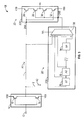
Figure 1 is a simplified schematic of an interleaved transient filter; -
Figure 2 is a simplified layout showing a position of transistors used in a C-gate for the interleaved transient filter ofFigure 1 ; -
Figure 3 is another simplified schematic of an interleaved transient filter; -
Figure 4 is a simplified schematic of the interleaved transient filter ofFigure 3 , showing one implementation of a delay circuit; and -
Figure 5 is a simplified layout showing a position of transistors used in a C-gate for the interleaved transient filter ofFigure 3 and4 ; -
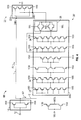
Figure 6 is another simplified schematic of an interleaved transient filter; -
Figure 7 is a simplified schematic of the interleaved transient filter ofFigure 6 , showing one implementation of a delay circuit; and -
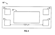
Figure 8 is a simplified layout showing a position of transistors used in a C-gate for the interleaved transient filter ofFigure 3 and4 . - Referring to
Figure 1 and2 , an interleaved transient filter 10 (hereinafter filter 10) may be described. Thefilter 10 may be configured to remove voltage transients on aninput 12 of thefilter 10 due to radiation Single Event Transient (SETs) or due to cross talk whose duration may be less than a delay of adelay element 20 in thefilter 10. - The
filter 10 may send an input signal A oninput 12 to aninput buffer 14. In the present embodiment, theinput buffer 14 may be formed of a pair oftransistors transistors transistor 16 may be a P-type transistor such as a P-type MOSFET, while thetransistor 18 may be an N-type transistor such as an N-type MOSFET. - When the input signal A is a high signal,
transistor 18 may turn on and send the input signal A along two paths, path 1 having signal A1 andpath 2 having signal A2. Similarly, when the input signal A is a low signal,transistor 16 may turn on and send the input signal A along two paths, path 1 having signal A1 andpath 2 having signal A2.Path 2 may include adelay element 20. The two signals A1 and A2 along path 1 andpath 2 respectively may be sent toinputs logic element 22. Thelogic element 22 may be aC-gate 22A. - When the signals A1 and A2 sent to
inputs C-gate 22A match, the C-gate 22A may act as an inverter. When the signals A1 and A2 sent toinputs C-gate 22A do not match, theC-gate 22A may not drive its output (high impedance state), and the output of theC-gate 22A may maintain its current value. - In the embodiment shown, the
C-gate 22A may be comprised of twoseries PMOS transistors series NMOS transistors input C-gate 22A controls the gate of onePMOS transistor NMOS transistor input 24A can control the gate ofPMOS transistor 26 and the gate ofNMOS transistor 32. Theinput 24B can control the gate ofPMOS transistor 28 and the gate ofNMOS transistor 30. - To generate an SET at an output of the
filter 10, a radiation particle would generally have to strike either bothseries NMOS transistors series PMOS transistors filter 10. TheC-gate PMOS transistors NMOS transistors - Current Silicon-On-Insulator (SOI) technologies may have very thin epitaxial silicon layers on top of the buried oxide (BOX), generally less than 100 nm starting at the 90-nm process node. Consequently, the spacing needed to reduce double-node strikes to an acceptable level may be approximately 0.5 microns, which may be attained by interleaving the
PMOS transistors NMOS transistors C-gate 22A. Thedelay element 20 may be placed between the interleavedPMOS transistors NMOS transistors C-gate 22A, in order to achieve the desired node spacing without any wasted space. - As may be seen in
Figure 1 , a first implementation of thefilter 10 may use adelay element 20 which is a fixeddelay element 20A. The fixeddelay element 20A may be comprised of a plurality of series connectedtransistor delay circuits 34. The duration of the fixeddelay element 20A may be selected during the design phase of an Application Specific Integrated Circuit (ASIC). The delay time may be a function of process, voltage and temperature. For instance, if the ASIC is manufactured in a slow corner the delay may be greater, but commensurate with the type of transients generated by the logic circuits in the ASIC. - Referring now to
Figures 3-5 , a second implementation of the filter 10' may be shown. Like thefilter 10, the filter 10' may send an input signal A to aninput buffer 14. In the embodiment shown, theinput buffer 14 may be formed of a pair oftransistors transistors transistor 16 may be a P-type MOSFET while thetransistor 18 may be an N-type MOSFET. - When the input signal A is a high signal,
transistor 18 may turn on and send the input signal A along two paths, path 1 having signal A1 andpath 2 having signal A2. Similarly, when the input signal A is a low signal,transistor 16 may turn on and send the input signal A along two paths, path 1 having signal A1 andpath 2 having signal A2.Path 2 may include adelay element 20'. The two signals A1 and A2 along path 1 andpath 2 respectively may be sent toinputs logic element 22. Thelogic element 22 may be a C-gate 22A. - When the signals A1 and A2 sent to
inputs C-gate 22A match, theC-gate 22A may act as an inverter. When the signals A1 and A2 sent toinputs C-gate 22A do not match, theC-gate 22A may not drive its output (high impedance state), and the output of theC-gate 22A may maintain its current value. - In the embodiment shown, the
C-gate 22A may be comprised of twoseries PMOS transistors series NMOS transistors input C-gate 22A controls the gate of onePMOS transistor NMOS transistor input 24A can control the gate ofPMOS transistor 26 and the gate ofNMOS transistor 32. Theinput 24B can control the gate ofPMOS transistor 28 and the gate ofNMOS transistor 30. - To generate an SET at an output of the filter 10', a radiation particle would generally have to strike either both
series NMOS transistors series PMOS transistors C-gate PMOS transistors NMOS transistors - As described above, current SOI technologies may have very thin epitaxial silicon layers on top of the buried oxide (BOX), generally less than 100 nm starting at the 90-nm process node, so the spacing needed to reduce double-node strikes to an acceptable level may be approximately 0.5 microns. This may be attained by interleaving the
PMOS transistors NMOS transistors C-gate 22A. Similar to delayelement 20, thedelay element 20' may also be placed between the interleavedPMOS transistors NMOS transistors C-gate 22A, in order to achieve the desired node spacing without any wasted space. - As may be seen in
Figures 3 and4 , thedelay element 20' is aselectable delay element 20B. Theselectable delay element 20B may be comprised of a plurality of fixeddelay circuits 36. Each fixeddelay circuits 36 may be comprised of series connectedtransistor delay circuits 34 similar to that shown for the fixeddelay element 20A shown inFigure 1 . The duration of each fixeddelay circuit 36 may be selected during the design phase of an ASIC. The delay may be a function of process, voltage and temperature. - Each of the fixed
delay circuits 36 may be coupled to amultiplexer 38. The fixeddelay circuits 36 may be placed serially back to back with the output of each fixeddelay circuit 36 coupled to an input of themultiplexer 38 and to the input of the subsequentfixed delay circuit 36. The output of themultiplexer 38 may be connected to thesecond input 24B of theC-gate 22A. One or more select signals SEL may be sent to themultiplexer 38 and may be used to configure theselectable delay element 20B to a user selected, desired programmable time delay. The select signals SEL may be used to send signals to themultiplexer 38 to select which outputs from the fixeddelay circuits 36 are sent to thesecond input 24B of theC-gate 22A. - Referring now to
Figures 6-8 , another implementation of thefilter 10" may be shown. Like thefilter 10 and 10', thefilter 10" may send an input signal A to aninput buffer 14. In the embodiment shown, theinput buffer 14 may be formed of a pair oftransistors transistors transistor 16 may be a P-type MOSFET while thetransistor 18 may be an N-type MOSFET. - When the input signal A is a high signal,
transistor 18 may turn on and send the input signal A along two paths, path 1 having signal A1 andpath 2 having signal A2. Similarly, when the input signal A is a low signal,transistor 16 may turn on and send the input signal A along two paths, path 1 having signal A1 andpath 2 having signal A2.Path 2 may include adelay element 20". The two signals A1 and A2 along path 1 andpath 2 respectively may be sent toinputs logic element 22. Thelogic element 22 may be a C-gate 22A. - When the signals A1 and A2 sent to
inputs C-gate 22A match, theC-gate 22A may act as an inverter. When the signals A1 and A2 sent toinputs C-gate 22A do not match, theC-gate 22A may not drive its output (high impedance state), and the output of theC-gate 22A may maintain its current value. - In the embodiment shown, the
C-gate 22A may be comprised of twoseries PMOS transistors series NMOS transistors input C-gate 22A controls the gate of onePMOS transistor NMOS transistor input 24A can control the gate ofPMOS transistor 26 and the gate ofNMOS transistor 32. Theinput 24B can control the gate ofPMOS transistor 28 and the gate ofNMOS transistor 30. - To generate an SET at an output of the
filter 10", a radiation particle would generally have to strike either bothseries NMOS transistors series PMOS transistors filter 10". TheC-gate PMOS transistors NMOS transistors - As described above, current SOI technologies may have very thin epitaxial silicon layers on top of the buried oxide (BOX), generally less than 100 nm starting at the 90-nm process node, so the spacing needed to reduce double-node strikes to an acceptable level may be approximately 0.5 microns. This may be attained by interleaving the
PMOS transistors NMOS transistors C-gate 22A. Similar to delayelements delay element 20" may be placed between the interleavedPMOS transistors NMOS transistors C-gate 22A, in order to achieve the desired node spacing without any wasted space. - As may be seen in
Figures 6 and7 , thedelay element 20" is aprogrammable delay element 20C. Theprogrammable delay element 20C may have aprogrammable delay unit 40 for providing a programmable delay amount. Theprogrammable delay unit 40 may haveseveral transistor stacks 42 and acurrent mirror 44 that controls the amount of tail current flowing through theprogrammable delay unit 40. In this embodiment, thefilter 10" may be programmed to filter transients of a specific delay, regardless of process, voltage and temperature variability. Theprogrammable delay unit 40 may need a minimum of three programming signals. Two signals, S0 and S1, may be used to control the current bias into thecurrent mirror 44. A third signal, S2, may be used as an additional switch that gives two different configurations of the tail current in the delay element. The design is implemented with transistors of multiple threshold voltages to generate various delay bins. - While embodiments of the disclosure have been described in terms of various specific embodiments, those skilled in the art will recognize that the embodiments of the disclosure may be practiced with modifications within the spirit and scope of the claims.
Claims (15)
- An interleaved filter circuit, comprising:a delay element configured to receive an input signal; andan interleaved output buffer having a first input which receives the input signal, a second input which receives the output of the delay element, an output of the interleaved output buffer driven when the first input and the second input are at a same logic level.
- The interleaved filter circuit in accordance with Claim 1, wherein the interleaved output buffer comprises:a first pair of transistors coupled to the input signal; anda second pair of transistors coupled to the output of the delay element;wherein the first pair of transistors and the second pair of transistors are interleaved.
- The interleaved filter circuit in accordance with Claim 1, wherein the interleaved output buffer comprises:a first pair of transistors coupled to the input signal, wherein the first pair of transistors are a first P-type transistor and a first N-type transistor; anda second pair of transistors coupled to the output of the delay element, wherein the second pair of transistors are a second P-type transistor and a second N-type transistor;wherein the first N-type transistor and the second N-type transistor are interleaved and the first P-type transistor and the second P-type transistor are interleaved.
- The interleaved filter circuit in accordance with Claim 1, wherein the interleaved output buffer comprises:a first pair of transistors coupled to the input signal, wherein the first pair of transistors are a first PMOSFET and first NMOSFET; anda second pair of transistors coupled to the output of the delay element, wherein the second pair of transistors are a second PMOSFET and a second NMOSFET;wherein the first NMOSFET is interleaved with the second NMOSFET and the first PMOSFET is interleaved with the second PMOSFET.
- The interleaved filter circuit in accordance with Claim 1, wherein the delay element provides a fixed time delay.
- The interleaved filter circuit in accordance with Claim 1, wherein the delay element provides a programmable time delay.
- The interleaved filter circuit in accordance with Claim l, wherein the delay element provides a user selected time delay.
- The interleaved filter circuit in accordance with Claim 1, wherein the delay element comprises:a multiplexer; anda plurality of cascaded delay elements, an output of each of the plurality of cascaded delay elements coupled to the multiplexer.
- The interleaved filter circuit in accordance with Claim 1, wherein the delay element comprises:a multiplexer; anda programmable delay element coupled to the multiplexer, the output of the delay element being determined by a programmable delay amount selected for the programmable delay element.
- The interleaved filter circuit in accordance with Claim 9, wherein the programmable delay element comprises:a plurality of transistor stacks; anda current mirror to control an amount of tail current flowing through the programmable delay element.
- A method for filtering Single Event Transients (SETs), the method comprising:providing an output buffer having a first pair of transistors wherein the first pair of transistors are a first PMOSFET and first NMOSFET and a second pair of transistors wherein the second pair of transistors are a second PMOSFET and a second NMOSFET, the first and second NMOSFETs being interleaved, the first and second PMOSFETs being interleaved;sending an input signal to the first pair of transistors;delaying the input signal by a predetermined amount of time to the second pair of transistors to form a delayed input signal; anddriving an output buffer output signal when the input signal and the delayed input signal are at a same logic level.
- The method of Claim 11, wherein delaying the input signal comprises sending the input signal to a delay element.
- The method of Claim 11, wherein the delay element provides a fixed time delay.
- The method of Claim 11, wherein the delay element is programmable.
- The method of Claim 14, wherein the delay element provides a user selected time delay.
Applications Claiming Priority (1)
| Application Number | Priority Date | Filing Date | Title |
|---|---|---|---|
| US13/673,438 US8754701B2 (en) | 2012-11-09 | 2012-11-09 | Interleaved transient filter |
Publications (3)
| Publication Number | Publication Date |
|---|---|
| EP2731267A2 true EP2731267A2 (en) | 2014-05-14 |
| EP2731267A3 EP2731267A3 (en) | 2014-07-30 |
| EP2731267B1 EP2731267B1 (en) | 2020-09-23 |
Family
ID=49758986
Family Applications (1)
| Application Number | Title | Priority Date | Filing Date |
|---|---|---|---|
| EP13191756.9A Active EP2731267B1 (en) | 2012-11-09 | 2013-11-06 | Interleaved transient filter and method |
Country Status (5)
| Country | Link |
|---|---|
| US (1) | US8754701B2 (en) |
| EP (1) | EP2731267B1 (en) |
| KR (1) | KR102107851B1 (en) |
| SG (1) | SG2013082862A (en) |
| TW (1) | TWI597937B (en) |
Families Citing this family (1)
| Publication number | Priority date | Publication date | Assignee | Title |
|---|---|---|---|---|
| US11601119B2 (en) * | 2020-12-18 | 2023-03-07 | The Boeing Company | Radiation hardened flip-flop circuit for mitigating single event transients |
Family Cites Families (11)
| Publication number | Priority date | Publication date | Assignee | Title |
|---|---|---|---|---|
| US5867448A (en) * | 1997-06-11 | 1999-02-02 | Cypress Semiconductor Corp. | Buffer for memory modules with trace delay compensation |
| US6326809B1 (en) | 1999-09-27 | 2001-12-04 | University Of New Mexico | Apparatus for and method of eliminating single event upsets in combinational logic |
| US6504410B2 (en) | 2000-05-11 | 2003-01-07 | Goodrich Corporation | Fault tolerant storage cell |
| US6617936B2 (en) * | 2001-02-20 | 2003-09-09 | Velio Communications, Inc. | Phase controlled oscillator |
| US7415645B2 (en) | 2005-07-28 | 2008-08-19 | International Business Machines Corporation | Method and apparatus for soft-error immune and self-correcting latches |
| JP4332652B2 (en) | 2005-12-12 | 2009-09-16 | 独立行政法人 宇宙航空研究開発機構 | Single event resistant latch circuit and flip-flop circuit |
| US20080115023A1 (en) | 2006-10-27 | 2008-05-15 | Honeywell International Inc. | Set hardened register |
| US7928770B1 (en) * | 2006-11-06 | 2011-04-19 | Altera Corporation | I/O block for high performance memory interfaces |
| US8191021B2 (en) | 2008-01-28 | 2012-05-29 | Actel Corporation | Single event transient mitigation and measurement in integrated circuits |
| US8054099B2 (en) | 2009-07-29 | 2011-11-08 | The Boeing Company | Method and apparatus for reducing radiation and cross-talk induced data errors |
| US8847621B2 (en) * | 2012-07-16 | 2014-09-30 | The Boeing Company | Single event transient and upset mitigation for silicon-on-insulator CMOS technology |
-
2012
- 2012-11-09 US US13/673,438 patent/US8754701B2/en active Active
-
2013
- 2013-08-22 KR KR1020130099603A patent/KR102107851B1/en active Active
- 2013-11-06 EP EP13191756.9A patent/EP2731267B1/en active Active
- 2013-11-08 TW TW102140602A patent/TWI597937B/en active
- 2013-11-08 SG SG2013082862A patent/SG2013082862A/en unknown
Non-Patent Citations (1)
| Title |
|---|
| None |
Also Published As
| Publication number | Publication date |
|---|---|
| EP2731267A3 (en) | 2014-07-30 |
| SG2013082862A (en) | 2014-06-27 |
| US8754701B2 (en) | 2014-06-17 |
| TWI597937B (en) | 2017-09-01 |
| KR20140060219A (en) | 2014-05-19 |
| EP2731267B1 (en) | 2020-09-23 |
| KR102107851B1 (en) | 2020-05-08 |
| US20140132332A1 (en) | 2014-05-15 |
| TW201421902A (en) | 2014-06-01 |
Similar Documents
| Publication | Publication Date | Title |
|---|---|---|
| US11670941B2 (en) | Single-gate-oxide power inverter and electrostatic discharge protection circuit | |
| EP3357090B1 (en) | Electrostatic discharge protection device and circuit apparatus | |
| CN108604898B (en) | Input/output (I/O) driver implementing dynamic gate biasing of buffer transistors | |
| US20130070376A1 (en) | Electrostatic discharge protection circuit and electrostatic discharge protection method | |
| US8674740B2 (en) | Noise removing delay circuit | |
| EP1806846B1 (en) | High voltage digital driver with dynamically biased cascode transistors | |
| US20190006842A1 (en) | Protection circuit | |
| US12335068B2 (en) | Multi-channel digital isolator with integrated configurable pulse width modulation interlock protection | |
| US7755392B1 (en) | Level shift circuit without high voltage stress of transistors and operating at low voltages | |
| JPH10173499A (en) | Output driver circuit and semiconductor device | |
| US8754701B2 (en) | Interleaved transient filter | |
| CN105141303B (en) | Slope control circuit | |
| EP1454414B1 (en) | High-speed output circuit with low voltage capability | |
| TW201703437A (en) | Power-on-reset detector | |
| JP2010193246A (en) | Output buffer circuit | |
| JPH01240013A (en) | Semiconductor integrated circuit device | |
| JP2010273186A (en) | Delay circuit | |
| JP5979162B2 (en) | Power-on reset circuit | |
| KR20000074289A (en) | Level shifter for high voltage integrated circuits | |
| US9312860B1 (en) | Gated differential logic circuit | |
| US20160142051A1 (en) | Driver output with dynamic switching bias | |
| JP2014011677A (en) | Delay circuit | |
| JP2016167748A (en) | Output buffer circuit | |
| US6714055B2 (en) | Output driver devices | |
| US20060181313A1 (en) | Transistor logic circuit |
Legal Events
| Date | Code | Title | Description |
|---|---|---|---|
| PUAI | Public reference made under article 153(3) epc to a published international application that has entered the european phase |
Free format text: ORIGINAL CODE: 0009012 |
|
| 17P | Request for examination filed |
Effective date: 20131106 |
|
| AK | Designated contracting states |
Kind code of ref document: A2 Designated state(s): AL AT BE BG CH CY CZ DE DK EE ES FI FR GB GR HR HU IE IS IT LI LT LU LV MC MK MT NL NO PL PT RO RS SE SI SK SM TR |
|
| AX | Request for extension of the european patent |
Extension state: BA ME |
|
| PUAL | Search report despatched |
Free format text: ORIGINAL CODE: 0009013 |
|
| AK | Designated contracting states |
Kind code of ref document: A3 Designated state(s): AL AT BE BG CH CY CZ DE DK EE ES FI FR GB GR HR HU IE IS IT LI LT LU LV MC MK MT NL NO PL PT RO RS SE SI SK SM TR |
|
| AX | Request for extension of the european patent |
Extension state: BA ME |
|
| RIC1 | Information provided on ipc code assigned before grant |
Ipc: H03K 5/1252 20060101AFI20140623BHEP |
|
| STAA | Information on the status of an ep patent application or granted ep patent |
Free format text: STATUS: EXAMINATION IS IN PROGRESS |
|
| 17Q | First examination report despatched |
Effective date: 20180530 |
|
| GRAP | Despatch of communication of intention to grant a patent |
Free format text: ORIGINAL CODE: EPIDOSNIGR1 |
|
| STAA | Information on the status of an ep patent application or granted ep patent |
Free format text: STATUS: GRANT OF PATENT IS INTENDED |
|
| INTG | Intention to grant announced |
Effective date: 20190626 |
|
| GRAS | Grant fee paid |
Free format text: ORIGINAL CODE: EPIDOSNIGR3 |
|
| GRAJ | Information related to disapproval of communication of intention to grant by the applicant or resumption of examination proceedings by the epo deleted |
Free format text: ORIGINAL CODE: EPIDOSDIGR1 |
|
| GRAL | Information related to payment of fee for publishing/printing deleted |
Free format text: ORIGINAL CODE: EPIDOSDIGR3 |
|
| STAA | Information on the status of an ep patent application or granted ep patent |
Free format text: STATUS: EXAMINATION IS IN PROGRESS |
|
| INTC | Intention to grant announced (deleted) | ||
| GRAP | Despatch of communication of intention to grant a patent |
Free format text: ORIGINAL CODE: EPIDOSNIGR1 |
|
| STAA | Information on the status of an ep patent application or granted ep patent |
Free format text: STATUS: GRANT OF PATENT IS INTENDED |
|
| INTG | Intention to grant announced |
Effective date: 20200318 |
|
| GRAJ | Information related to disapproval of communication of intention to grant by the applicant or resumption of examination proceedings by the epo deleted |
Free format text: ORIGINAL CODE: EPIDOSDIGR1 |
|
| GRAL | Information related to payment of fee for publishing/printing deleted |
Free format text: ORIGINAL CODE: EPIDOSDIGR3 |
|
| STAA | Information on the status of an ep patent application or granted ep patent |
Free format text: STATUS: EXAMINATION IS IN PROGRESS |
|
| INTC | Intention to grant announced (deleted) | ||
| GRAR | Information related to intention to grant a patent recorded |
Free format text: ORIGINAL CODE: EPIDOSNIGR71 |
|
| STAA | Information on the status of an ep patent application or granted ep patent |
Free format text: STATUS: GRANT OF PATENT IS INTENDED |
|
| GRAA | (expected) grant |
Free format text: ORIGINAL CODE: 0009210 |
|
| STAA | Information on the status of an ep patent application or granted ep patent |
Free format text: STATUS: THE PATENT HAS BEEN GRANTED |
|
| INTG | Intention to grant announced |
Effective date: 20200812 |
|
| RIN1 | Information on inventor provided before grant (corrected) |
Inventor name: RABAA, SALIM A. Inventor name: CABANAS-HOLMEN, MANUEL F. Inventor name: CANNON, ETHAN |
|
| AK | Designated contracting states |
Kind code of ref document: B1 Designated state(s): AL AT BE BG CH CY CZ DE DK EE ES FI FR GB GR HR HU IE IS IT LI LT LU LV MC MK MT NL NO PL PT RO RS SE SI SK SM TR |
|
| REG | Reference to a national code |
Ref country code: GB Ref legal event code: FG4D |
|
| REG | Reference to a national code |
Ref country code: CH Ref legal event code: EP |
|
| REG | Reference to a national code |
Ref country code: DE Ref legal event code: R096 Ref document number: 602013072719 Country of ref document: DE |
|
| REG | Reference to a national code |
Ref country code: IE Ref legal event code: FG4D |
|
| REG | Reference to a national code |
Ref country code: AT Ref legal event code: REF Ref document number: 1317423 Country of ref document: AT Kind code of ref document: T Effective date: 20201015 |
|
| PG25 | Lapsed in a contracting state [announced via postgrant information from national office to epo] |
Ref country code: FI Free format text: LAPSE BECAUSE OF FAILURE TO SUBMIT A TRANSLATION OF THE DESCRIPTION OR TO PAY THE FEE WITHIN THE PRESCRIBED TIME-LIMIT Effective date: 20200923 Ref country code: NO Free format text: LAPSE BECAUSE OF FAILURE TO SUBMIT A TRANSLATION OF THE DESCRIPTION OR TO PAY THE FEE WITHIN THE PRESCRIBED TIME-LIMIT Effective date: 20201223 Ref country code: GR Free format text: LAPSE BECAUSE OF FAILURE TO SUBMIT A TRANSLATION OF THE DESCRIPTION OR TO PAY THE FEE WITHIN THE PRESCRIBED TIME-LIMIT Effective date: 20201224 Ref country code: BG Free format text: LAPSE BECAUSE OF FAILURE TO SUBMIT A TRANSLATION OF THE DESCRIPTION OR TO PAY THE FEE WITHIN THE PRESCRIBED TIME-LIMIT Effective date: 20201223 Ref country code: SE Free format text: LAPSE BECAUSE OF FAILURE TO SUBMIT A TRANSLATION OF THE DESCRIPTION OR TO PAY THE FEE WITHIN THE PRESCRIBED TIME-LIMIT Effective date: 20200923 Ref country code: HR Free format text: LAPSE BECAUSE OF FAILURE TO SUBMIT A TRANSLATION OF THE DESCRIPTION OR TO PAY THE FEE WITHIN THE PRESCRIBED TIME-LIMIT Effective date: 20200923 |
|
| REG | Reference to a national code |
Ref country code: AT Ref legal event code: MK05 Ref document number: 1317423 Country of ref document: AT Kind code of ref document: T Effective date: 20200923 |
|
| PG25 | Lapsed in a contracting state [announced via postgrant information from national office to epo] |
Ref country code: RS Free format text: LAPSE BECAUSE OF FAILURE TO SUBMIT A TRANSLATION OF THE DESCRIPTION OR TO PAY THE FEE WITHIN THE PRESCRIBED TIME-LIMIT Effective date: 20200923 Ref country code: LV Free format text: LAPSE BECAUSE OF FAILURE TO SUBMIT A TRANSLATION OF THE DESCRIPTION OR TO PAY THE FEE WITHIN THE PRESCRIBED TIME-LIMIT Effective date: 20200923 |
|
| REG | Reference to a national code |
Ref country code: NL Ref legal event code: MP Effective date: 20200923 |
|
| REG | Reference to a national code |
Ref country code: LT Ref legal event code: MG4D |
|
| PG25 | Lapsed in a contracting state [announced via postgrant information from national office to epo] |
Ref country code: CZ Free format text: LAPSE BECAUSE OF FAILURE TO SUBMIT A TRANSLATION OF THE DESCRIPTION OR TO PAY THE FEE WITHIN THE PRESCRIBED TIME-LIMIT Effective date: 20200923 Ref country code: EE Free format text: LAPSE BECAUSE OF FAILURE TO SUBMIT A TRANSLATION OF THE DESCRIPTION OR TO PAY THE FEE WITHIN THE PRESCRIBED TIME-LIMIT Effective date: 20200923 Ref country code: PT Free format text: LAPSE BECAUSE OF FAILURE TO SUBMIT A TRANSLATION OF THE DESCRIPTION OR TO PAY THE FEE WITHIN THE PRESCRIBED TIME-LIMIT Effective date: 20210125 Ref country code: LT Free format text: LAPSE BECAUSE OF FAILURE TO SUBMIT A TRANSLATION OF THE DESCRIPTION OR TO PAY THE FEE WITHIN THE PRESCRIBED TIME-LIMIT Effective date: 20200923 Ref country code: NL Free format text: LAPSE BECAUSE OF FAILURE TO SUBMIT A TRANSLATION OF THE DESCRIPTION OR TO PAY THE FEE WITHIN THE PRESCRIBED TIME-LIMIT Effective date: 20200923 Ref country code: RO Free format text: LAPSE BECAUSE OF FAILURE TO SUBMIT A TRANSLATION OF THE DESCRIPTION OR TO PAY THE FEE WITHIN THE PRESCRIBED TIME-LIMIT Effective date: 20200923 Ref country code: SM Free format text: LAPSE BECAUSE OF FAILURE TO SUBMIT A TRANSLATION OF THE DESCRIPTION OR TO PAY THE FEE WITHIN THE PRESCRIBED TIME-LIMIT Effective date: 20200923 |
|
| PG25 | Lapsed in a contracting state [announced via postgrant information from national office to epo] |
Ref country code: PL Free format text: LAPSE BECAUSE OF FAILURE TO SUBMIT A TRANSLATION OF THE DESCRIPTION OR TO PAY THE FEE WITHIN THE PRESCRIBED TIME-LIMIT Effective date: 20200923 Ref country code: IS Free format text: LAPSE BECAUSE OF FAILURE TO SUBMIT A TRANSLATION OF THE DESCRIPTION OR TO PAY THE FEE WITHIN THE PRESCRIBED TIME-LIMIT Effective date: 20210123 Ref country code: ES Free format text: LAPSE BECAUSE OF FAILURE TO SUBMIT A TRANSLATION OF THE DESCRIPTION OR TO PAY THE FEE WITHIN THE PRESCRIBED TIME-LIMIT Effective date: 20200923 Ref country code: AT Free format text: LAPSE BECAUSE OF FAILURE TO SUBMIT A TRANSLATION OF THE DESCRIPTION OR TO PAY THE FEE WITHIN THE PRESCRIBED TIME-LIMIT Effective date: 20200923 Ref country code: AL Free format text: LAPSE BECAUSE OF FAILURE TO SUBMIT A TRANSLATION OF THE DESCRIPTION OR TO PAY THE FEE WITHIN THE PRESCRIBED TIME-LIMIT Effective date: 20200923 |
|
| REG | Reference to a national code |
Ref country code: DE Ref legal event code: R097 Ref document number: 602013072719 Country of ref document: DE |
|
| PG25 | Lapsed in a contracting state [announced via postgrant information from national office to epo] |
Ref country code: SK Free format text: LAPSE BECAUSE OF FAILURE TO SUBMIT A TRANSLATION OF THE DESCRIPTION OR TO PAY THE FEE WITHIN THE PRESCRIBED TIME-LIMIT Effective date: 20200923 Ref country code: MC Free format text: LAPSE BECAUSE OF FAILURE TO SUBMIT A TRANSLATION OF THE DESCRIPTION OR TO PAY THE FEE WITHIN THE PRESCRIBED TIME-LIMIT Effective date: 20200923 |
|
| REG | Reference to a national code |
Ref country code: CH Ref legal event code: PL |
|
| PG25 | Lapsed in a contracting state [announced via postgrant information from national office to epo] |
Ref country code: LU Free format text: LAPSE BECAUSE OF NON-PAYMENT OF DUE FEES Effective date: 20201106 |
|
| PLBE | No opposition filed within time limit |
Free format text: ORIGINAL CODE: 0009261 |
|
| STAA | Information on the status of an ep patent application or granted ep patent |
Free format text: STATUS: NO OPPOSITION FILED WITHIN TIME LIMIT |
|
| REG | Reference to a national code |
Ref country code: BE Ref legal event code: MM Effective date: 20201130 |
|
| PG25 | Lapsed in a contracting state [announced via postgrant information from national office to epo] |
Ref country code: DK Free format text: LAPSE BECAUSE OF FAILURE TO SUBMIT A TRANSLATION OF THE DESCRIPTION OR TO PAY THE FEE WITHIN THE PRESCRIBED TIME-LIMIT Effective date: 20200923 Ref country code: CH Free format text: LAPSE BECAUSE OF NON-PAYMENT OF DUE FEES Effective date: 20201130 Ref country code: LI Free format text: LAPSE BECAUSE OF NON-PAYMENT OF DUE FEES Effective date: 20201130 Ref country code: SI Free format text: LAPSE BECAUSE OF FAILURE TO SUBMIT A TRANSLATION OF THE DESCRIPTION OR TO PAY THE FEE WITHIN THE PRESCRIBED TIME-LIMIT Effective date: 20200923 |
|
| 26N | No opposition filed |
Effective date: 20210624 |
|
| PG25 | Lapsed in a contracting state [announced via postgrant information from national office to epo] |
Ref country code: IE Free format text: LAPSE BECAUSE OF NON-PAYMENT OF DUE FEES Effective date: 20201106 Ref country code: IT Free format text: LAPSE BECAUSE OF FAILURE TO SUBMIT A TRANSLATION OF THE DESCRIPTION OR TO PAY THE FEE WITHIN THE PRESCRIBED TIME-LIMIT Effective date: 20200923 |
|
| PG25 | Lapsed in a contracting state [announced via postgrant information from national office to epo] |
Ref country code: TR Free format text: LAPSE BECAUSE OF FAILURE TO SUBMIT A TRANSLATION OF THE DESCRIPTION OR TO PAY THE FEE WITHIN THE PRESCRIBED TIME-LIMIT Effective date: 20200923 Ref country code: MT Free format text: LAPSE BECAUSE OF FAILURE TO SUBMIT A TRANSLATION OF THE DESCRIPTION OR TO PAY THE FEE WITHIN THE PRESCRIBED TIME-LIMIT Effective date: 20200923 Ref country code: CY Free format text: LAPSE BECAUSE OF FAILURE TO SUBMIT A TRANSLATION OF THE DESCRIPTION OR TO PAY THE FEE WITHIN THE PRESCRIBED TIME-LIMIT Effective date: 20200923 |
|
| PG25 | Lapsed in a contracting state [announced via postgrant information from national office to epo] |
Ref country code: MK Free format text: LAPSE BECAUSE OF FAILURE TO SUBMIT A TRANSLATION OF THE DESCRIPTION OR TO PAY THE FEE WITHIN THE PRESCRIBED TIME-LIMIT Effective date: 20200923 |
|
| PG25 | Lapsed in a contracting state [announced via postgrant information from national office to epo] |
Ref country code: BE Free format text: LAPSE BECAUSE OF NON-PAYMENT OF DUE FEES Effective date: 20201130 |
|
| P01 | Opt-out of the competence of the unified patent court (upc) registered |
Effective date: 20230516 |
|
| PGFP | Annual fee paid to national office [announced via postgrant information from national office to epo] |
Ref country code: DE Payment date: 20251128 Year of fee payment: 13 |
|
| PGFP | Annual fee paid to national office [announced via postgrant information from national office to epo] |
Ref country code: GB Payment date: 20251127 Year of fee payment: 13 |
|
| PGFP | Annual fee paid to national office [announced via postgrant information from national office to epo] |
Ref country code: FR Payment date: 20251125 Year of fee payment: 13 |