EP2731199B1 - Connector - Google Patents
Connector Download PDFInfo
- Publication number
- EP2731199B1 EP2731199B1 EP13191896.3A EP13191896A EP2731199B1 EP 2731199 B1 EP2731199 B1 EP 2731199B1 EP 13191896 A EP13191896 A EP 13191896A EP 2731199 B1 EP2731199 B1 EP 2731199B1
- Authority
- EP
- European Patent Office
- Prior art keywords
- section
- contacts
- connector
- insertion section
- cam
- Prior art date
- Legal status (The legal status is an assumption and is not a legal conclusion. Google has not performed a legal analysis and makes no representation as to the accuracy of the status listed.)
- Active
Links
- 238000003780 insertion Methods 0.000 claims description 176
- 230000037431 insertion Effects 0.000 claims description 176
- 230000013011 mating Effects 0.000 claims description 76
- 238000000034 method Methods 0.000 claims description 2
- 239000002184 metal Substances 0.000 description 3
- 230000000903 blocking effect Effects 0.000 description 2
- 230000007257 malfunction Effects 0.000 description 2
- 230000003247 decreasing effect Effects 0.000 description 1
- 239000012212 insulator Substances 0.000 description 1
Images


Classifications
-
- H—ELECTRICITY
- H01—ELECTRIC ELEMENTS
- H01R—ELECTRICALLY-CONDUCTIVE CONNECTIONS; STRUCTURAL ASSOCIATIONS OF A PLURALITY OF MUTUALLY-INSULATED ELECTRICAL CONNECTING ELEMENTS; COUPLING DEVICES; CURRENT COLLECTORS
- H01R13/00—Details of coupling devices of the kinds covered by groups H01R12/70 or H01R24/00 - H01R33/00
- H01R13/62—Means for facilitating engagement or disengagement of coupling parts or for holding them in engagement
- H01R13/629—Additional means for facilitating engagement or disengagement of coupling parts, e.g. aligning or guiding means, levers, gas pressure electrical locking indicators, manufacturing tolerances
- H01R13/631—Additional means for facilitating engagement or disengagement of coupling parts, e.g. aligning or guiding means, levers, gas pressure electrical locking indicators, manufacturing tolerances for engagement only
-
- H—ELECTRICITY
- H01—ELECTRIC ELEMENTS
- H01R—ELECTRICALLY-CONDUCTIVE CONNECTIONS; STRUCTURAL ASSOCIATIONS OF A PLURALITY OF MUTUALLY-INSULATED ELECTRICAL CONNECTING ELEMENTS; COUPLING DEVICES; CURRENT COLLECTORS
- H01R13/00—Details of coupling devices of the kinds covered by groups H01R12/70 or H01R24/00 - H01R33/00
- H01R13/02—Contact members
- H01R13/15—Pins, blades or sockets having separate spring member for producing or increasing contact pressure
- H01R13/187—Pins, blades or sockets having separate spring member for producing or increasing contact pressure with spring member in the socket
-
- H—ELECTRICITY
- H01—ELECTRIC ELEMENTS
- H01R—ELECTRICALLY-CONDUCTIVE CONNECTIONS; STRUCTURAL ASSOCIATIONS OF A PLURALITY OF MUTUALLY-INSULATED ELECTRICAL CONNECTING ELEMENTS; COUPLING DEVICES; CURRENT COLLECTORS
- H01R12/00—Structural associations of a plurality of mutually-insulated electrical connecting elements, specially adapted for printed circuits, e.g. printed circuit boards [PCB], flat or ribbon cables, or like generally planar structures, e.g. terminal strips, terminal blocks; Coupling devices specially adapted for printed circuits, flat or ribbon cables, or like generally planar structures; Terminals specially adapted for contact with, or insertion into, printed circuits, flat or ribbon cables, or like generally planar structures
- H01R12/70—Coupling devices
- H01R12/82—Coupling devices connected with low or zero insertion force
- H01R12/85—Coupling devices connected with low or zero insertion force contact pressure producing means, contacts activated after insertion of printed circuits or like structures
- H01R12/89—Coupling devices connected with low or zero insertion force contact pressure producing means, contacts activated after insertion of printed circuits or like structures acting manually by moving connector housing parts linearly, e.g. slider
-
- H—ELECTRICITY
- H01—ELECTRIC ELEMENTS
- H01R—ELECTRICALLY-CONDUCTIVE CONNECTIONS; STRUCTURAL ASSOCIATIONS OF A PLURALITY OF MUTUALLY-INSULATED ELECTRICAL CONNECTING ELEMENTS; COUPLING DEVICES; CURRENT COLLECTORS
- H01R13/00—Details of coupling devices of the kinds covered by groups H01R12/70 or H01R24/00 - H01R33/00
- H01R13/62—Means for facilitating engagement or disengagement of coupling parts or for holding them in engagement
- H01R13/639—Additional means for holding or locking coupling parts together, after engagement, e.g. separate keylock, retainer strap
-
- H—ELECTRICITY
- H01—ELECTRIC ELEMENTS
- H01R—ELECTRICALLY-CONDUCTIVE CONNECTIONS; STRUCTURAL ASSOCIATIONS OF A PLURALITY OF MUTUALLY-INSULATED ELECTRICAL CONNECTING ELEMENTS; COUPLING DEVICES; CURRENT COLLECTORS
- H01R24/00—Two-part coupling devices, or either of their cooperating parts, characterised by their overall structure
- H01R24/20—Coupling parts carrying sockets, clips or analogous contacts and secured only to wire or cable
-
- G—PHYSICS
- G06—COMPUTING; CALCULATING OR COUNTING
- G06K—GRAPHICAL DATA READING; PRESENTATION OF DATA; RECORD CARRIERS; HANDLING RECORD CARRIERS
- G06K13/00—Conveying record carriers from one station to another, e.g. from stack to punching mechanism
- G06K13/02—Conveying record carriers from one station to another, e.g. from stack to punching mechanism the record carrier having longitudinal dimension comparable with transverse dimension, e.g. punched card
- G06K13/08—Feeding or discharging cards
- G06K13/0806—Feeding or discharging cards using an arrangement for ejection of an inserted card
- G06K13/0831—Feeding or discharging cards using an arrangement for ejection of an inserted card the ejection arrangement comprising a slide, carriage or drawer
-
- G—PHYSICS
- G06—COMPUTING; CALCULATING OR COUNTING
- G06K—GRAPHICAL DATA READING; PRESENTATION OF DATA; RECORD CARRIERS; HANDLING RECORD CARRIERS
- G06K13/00—Conveying record carriers from one station to another, e.g. from stack to punching mechanism
- G06K13/02—Conveying record carriers from one station to another, e.g. from stack to punching mechanism the record carrier having longitudinal dimension comparable with transverse dimension, e.g. punched card
- G06K13/08—Feeding or discharging cards
- G06K13/085—Feeding or discharging cards using an arrangement for locking the inserted card
-
- G—PHYSICS
- G06—COMPUTING; CALCULATING OR COUNTING
- G06K—GRAPHICAL DATA READING; PRESENTATION OF DATA; RECORD CARRIERS; HANDLING RECORD CARRIERS
- G06K7/00—Methods or arrangements for sensing record carriers, e.g. for reading patterns
- G06K7/0013—Methods or arrangements for sensing record carriers, e.g. for reading patterns by galvanic contacts, e.g. card connectors for ISO-7816 compliant smart cards or memory cards, e.g. SD card readers
- G06K7/0021—Methods or arrangements for sensing record carriers, e.g. for reading patterns by galvanic contacts, e.g. card connectors for ISO-7816 compliant smart cards or memory cards, e.g. SD card readers for reading/sensing record carriers having surface contacts
-
- H—ELECTRICITY
- H01—ELECTRIC ELEMENTS
- H01R—ELECTRICALLY-CONDUCTIVE CONNECTIONS; STRUCTURAL ASSOCIATIONS OF A PLURALITY OF MUTUALLY-INSULATED ELECTRICAL CONNECTING ELEMENTS; COUPLING DEVICES; CURRENT COLLECTORS
- H01R13/00—Details of coupling devices of the kinds covered by groups H01R12/70 or H01R24/00 - H01R33/00
- H01R13/02—Contact members
- H01R13/22—Contacts for co-operating by abutting
- H01R13/24—Contacts for co-operating by abutting resilient; resiliently-mounted
- H01R13/2442—Contacts for co-operating by abutting resilient; resiliently-mounted with a single cantilevered beam
-
- H—ELECTRICITY
- H01—ELECTRIC ELEMENTS
- H01R—ELECTRICALLY-CONDUCTIVE CONNECTIONS; STRUCTURAL ASSOCIATIONS OF A PLURALITY OF MUTUALLY-INSULATED ELECTRICAL CONNECTING ELEMENTS; COUPLING DEVICES; CURRENT COLLECTORS
- H01R13/00—Details of coupling devices of the kinds covered by groups H01R12/70 or H01R24/00 - H01R33/00
- H01R13/62—Means for facilitating engagement or disengagement of coupling parts or for holding them in engagement
- H01R13/629—Additional means for facilitating engagement or disengagement of coupling parts, e.g. aligning or guiding means, levers, gas pressure electrical locking indicators, manufacturing tolerances
- H01R13/633—Additional means for facilitating engagement or disengagement of coupling parts, e.g. aligning or guiding means, levers, gas pressure electrical locking indicators, manufacturing tolerances for disengagement only
- H01R13/635—Additional means for facilitating engagement or disengagement of coupling parts, e.g. aligning or guiding means, levers, gas pressure electrical locking indicators, manufacturing tolerances for disengagement only by mechanical pressure, e.g. spring force
Definitions
- the present invention relates to a connector including a contact for making contact with a connection pad of a mating connector inserted into an insertion receiving section for receiving the mating connector therein.
- the low-insertion-force type connector can be mated with a mating connector by a small force since mating completion is performed by, for example, a lever operation and the like, and thus, the low-insertion-force type connector is suitable for one having many contacts.
- a connector of such type requires not only an operation of mating a mating connector, but also, subsequently, an operation of, for example, a lever operation and the like, and thus, requires operations two times for mating once.
- the connection needs to include members such as a lever member, a member for operating the lever member and the like are required, and further, an indicator for remembering a second operation (for example, a lever operation) and other schemes are also required, and thus, such connector tends to have a complicated configuration.
- JP H09 251878 A discloses a connector according to the preamble of claim 1.
- US 2011/0021079 discloses also an electrical card connector comprising a housing including contacts, and a slider.
- the contacts are configured to be spaced from a first surface of an SD card when the SD card is initially inserted into an insertion receiving section of the housing by parts of the contacts resiliently engaging an inclined surface of a blocking portion of the slider.
- the slider has a pair of arms configured to be engaged by the SD card so that the slider is moved in the same direction as the SD card when the SD card is inserted into the connector. As the slider is moved, the blocking portion is moved away from the contacts so that the contacts spring through slots in the slider into engagement with the SD card.
- US 2002/0070274 discloses an IC card reading connector having a body containing a plurality of terminals.
- the body holds a movable flat block and the block has trenches for receiving the terminals which are biased towards the top side of the block on which an IC card is to rest.
- the movable flat block also has an IC card holding plate on its top side.
- the distal end of each terminal has a pair of protrusions wherein each protrusion engages an inclined guide surface on an underside of the movable flat block.
- JP 2009-152144 discloses a connector having first and second pairs of contacts. When a wiring board is inserted between the first pair of contacts, these contacts are pushed perpendicular to the direction of insertion of the wiring board. Each first contact pushes an insulator against a corresponding one of the second contacts so that a second pressing part of each second contact engages the wiring board.
- the present invention has been made to provide a connector whose mating is completed by only one insertion operation of a mating connector, and which has a configuration suitable for including many contacts.
- a connector includes: a housing including an insertion receiving section which is configured to receive a tabular insertion section of a mating connector having connection pads formed on a first surface of the insertion section; contacts configured to correspond to the connection pads, the contacts being configured to face the first surface when the insertion section of the mating connector is inserted into the insertion receiving section, and the contacts being configured to be spaced from the first surface when the insertion section is initially inserted into the insertion receiving section; and a pressing member being a slider, the slider configured to receive a force from the insertion section when the insertion section is at a final stage of insertion into the insertion receiving section, the slider including an abutment section which is configured to be engaged by the insertion section when the insertion section is inserted into the insertion receiving section so that the abutment section is moved in the same direction as the insertion section, the slider further including a cam section, the cam section being a cam plate having elongated openings through which the contacts pass,
- the connector according to the present invention includes the above-described pressing member, and thus, the contacts are pressed against the connection pads when moving to the final stage of inserting the mating connector into the insertion receiving section. For this reason, the insertion section does not suffer or just slightly suffers an interference from the contacts until the final stage of the insertion movement, and thus, the mating connector can be inserted by an small insertion force.
- the pressing member since the contacts receive a force from the insertion section to be connected to the connection pad in the final stage of the insertion movement, the mating is completed by only the insertion movement.
- pressing section including the abutment section and the cam section, pressing the contacts against the connection pads in the final stage of the insertion can be obtained with a simple structure.
- the connector having structure suitable for having multiple contacts is provided, in which the mating is completed by only one insertion operation of the mating connector.
- a method of mating connectors comprising the steps of: (a) providing a mating connector having a tabular insertion section and connection pads formed on a first surface of the insertion section; (b) providing a connector having a housing that includes an insertion receiving section to receive the tabular insertion section of the mating connector, contacts which correspond to the connection pads, and a pressing member being a slider and having an abutment section and a cam section, the cam section being a cam plate and having elongated openings through which the contacts pass, and cam surfaces formed on walls included in the respective elongated openings, the cam surfaces being orientated to extend obliquely towards the first surface when the insertion section is inserted into the insertion receiving section, and the cam surfaces being on the rear side in the insertion direction of the mating connector; and (c) inserting the insertion section of the mating connector into the insertion receiving section of the connector such that the contacts face the first surface, and wherein: (i) providing a mating connector having a tabular insertion
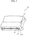
- FIG. 1 is an external perspective view of a connector of an embodiment according to the present invention.
- the connector 100 is covered with an outer shell 50 made of metal.
- An insertion opening 251 which is covered with a lid member 64 and into which a tabular insertion section of a mating connector is to be inserted is provided in a front wall 25 of a base housing 20 which is exposed toward the front.
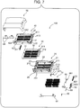
- FIG. 2 is an exploded perspective view illustrating the connector whose external view is illustrated in FIG. 1 where the connector is exploded into an outer shell (part (A)) and remaining components (part (B)).
- FIG. 3 is a perspective view illustrating the outer shell upside down.
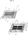
- FIG. 4 is an exploded perspective view illustrating an assembly remained by removing the outer shell from the connector according the present embodiment where the assembly is separated into an upper housing with a lid member (part (A)) and remaining components (part (B)).
- FIG. 5 is an exploded perspective view illustrating the upper housing with the lid member where the upper housing with the lid member is separated into the upper housing (part (A)) and the lid member (part (B)).
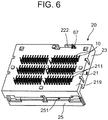
- FIG. 6 is a perspective view illustrating a base housing upside down in a state in which the contacts are press-fitted into the base housing.
- FIG. 7 is an exploded perspective view illustrating all of the components included in the connector according to the present embodiment whose assembled state is illustrated in FIG. 1 .
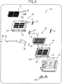
- FIG. 8 is an exploded perspective view illustrating the connector illustrated in FIG. 1 upside down while all of the components are separated from each other.
- the connector 100 includes plural contacts 10, a base housing 20, a slider 30, an upper housing 40 and an outer shell 50.
- the base housing 20 includes a bottom plate 21. Many elongated openings 211 which penetrate from a top surface through a bottom surface thereof are formed in the bottom plate 21.
- the contacts 10 are press-fitted into the elongated openings 211 from a side of a bottom surface of the bottom plate 21 (a side of the bottom surface 219 illustrated in FIG. 6 ).
- FIGS. 7 and 8 illustrate the contacts 10 in a state in which the contacts 10 are press-fitted into the respective elongated openings 211 to be aligned.
- Portions (see FIG. 6 ) of the contacts 10 which portions extend off from the bottom plate 21 to the side of the bottom surface 219 are to be connected to a circuit board (not illustrated) on which the connector 100 is to be placed.
- grooves 212, 213 are formed on the left and right in the bottom plate 21.
- a coil spring 61 is accommodated in the groove 212 on the left, and a cam member 62 in which a so-called heart cam groove is formed and a coil spring 63 are accommodated in the groove 213 on the right.
- One end of a cam bar 69 is inserted into the heart cam groove formed in the cam member 62. The other end of the cam bar 69 is supported by the base housing 20.
- the base housing 20 includes a rear wall 22, left and right walls 23, 24 and a front wall 25 upstanding so as to surround the bottom plate 21.
- An insertion opening 251 into which an insertion section of a mating connector is inserted is provided in the front wall 25.
- the lid member 64 which is supported by the upper housing 40 is arranged immediately inside the insertion opening 251, thereby forming a configuration in which the insertion opening 251 is closed by the lid member 64 (see FIG. 1 ).
- the lid member 64 has a configuration in which the lid member 64 is pressed by a tip of the insertion section of the mating connector from the outside to be rotated inwardly upward so as to open the insertion opening 251, and when the mating connector is removed, the lid member 64 closes the insertion opening 251 by an action of a torsion spring 65.
- the slider 30 is arranged on the bottom plate 21 of the base housing 20 as illustrated in part (B) of FIG. 4 .
- the slider 30 includes a cam plate 31 and a standing wall 32 standing at a side of a rear end of the cam plate 31.
- Many elongated openings 311 which penetrate from the top surface to the bottom surface and through which the contacts 10 are allowed to pass as illustrated in part (B) of FIG. 4 , and an elongated opening 312 through which the cam member 62 is allowed to pass is formed in the cam plate 31.
- the cam plate 31 enters a state in which the cam plate 31 is pressed toward the front wall 25 by the two coil springs 61, 63 in the base housing 20.
- the coil spring 61 is accommodated in the groove 212 to directly press the slider 30 toward the front wall 25.
- the other coil spring 63 is arranged in the groove 213 of the base housing 20 to directly press the cam member 62.
- the cam member 62 is also placed in the elongated opening 312 of the slider 30. For this reason, the cam member 62 pressed by the coil spring 63 presses a wall of the elongated opening 312 in the slider 30, so that the slider 30 enters a state in which the slider 30 is pressed via the cam member 62 toward the front wall 25 in the base housing 20.
- the slider 30 corresponds to an example of the pressing member according to the present invention
- the standing wall 32 corresponds to an example of the abutment section according to the present invention
- the cam plate 31 corresponds to an example of the cam section according to the present invention.
- the upper housing 40 illustrated in part (A) of FIG. 4 is arranged on the slider 30, and furthermore, the outer shell 50 illustrated in part (A) of FIG. 2 covers the upper housing 40.
- the outer shell 50 is made of metal and is held at a ground potential, thereby serving for shielding the connector 100.
- the upper housing 40 includes an upper plate 41 and a front wall 42 standing from the upper plate 41 on a front side thereof.
- the upper plate 41 forms a space between the upper plate 41 and the base plate 21 of the base housing 20 in which space the slider 30 is disposed.
- Many elongated openings 411 which allow the contacts 10 to pass therethrough are formed in the upper plate 41, and in addition, an elongated opening 412 which allows the standing wall 32 of the slider 30 to pass therethrough is also formed in the upper plate 41.
- a bump section 621 is provided on the above-described cam member 62, and an elongated opening 413 which allows the bump section 621 of the cam member 62 to pass therethrough is also formed in the upper plate 41 of the upper housing 40.
- a receiving slot 421 which receives the insertion section of the mating housing which is inserted from the insertion opening 251 formed in the front wall 25 of the base housing 20 is formed in the front wall 42 of the upper housing 40.
- a supporting section 422 which rotatably supports the lid member 64 is provided in an upper portion of the receiving opening 421 of the front wall 42.
- the lid member 64 is supported by the supporting section 422 as illustrated in part (A) of FIG. 4 to be rotatable inwardly upward.
- the lid member 64 is biased in a direction of closing the insertion opening 251 of the base housing 20 by a torsion spring 65.
- the insertion section of the mating connector is inserted from the insertion opening 251 illustrated in FIG. 1 of the base housing 20.
- the insertion section pushes up the lid member 64 supported by the upper housing 40 and is inserted onto the upper housing 40 of the assembly as assembled in the state as illustrated in part (B) of FIG. 2 from the receiving opening 421 of the upper housing 40.
- a tip of the inserted insertion section of the mating connector first bumps against the bump section 621 of the cam member 62 to slide the cam member 62 toward the depth against the biasing of the coil spring 63.
- the tip of the insertion section of the mating connector bumps against the bump section 621 of the cam member 62 and also against the standing wall 32 of the slider 30. For this reason, the tip of the insertion section slides the cam member 62 and the slider 30 together toward the depth against the biasing of the two coil springs 61, 63.
- the space over the upper plate 41 of the upper housing 40 i.e., the space between the upper plate 41 and the outer shell 50 which is put over the upper plate 41 to cover the upper plate 41 corresponds to an example of the "an insertion receiving section" to receive the mating connector.
- top ends of the contacts 10 have such shapes that, before the insertion section of the mating connector is inserted, the top ends of the contacts 10 are positioned inside the elongated openings 411 which are provided in the upper plate 41 of the upper housing 40 and allows the contacts 10 to pass therethrough, and do not protrude from the upper surface of the upper plate 41 (see part (B) of FIG. 2 ) .
- the contacts 10 are away or spaced from the insertion section when the insertion section of the mating connector is inserted, and are arranged at positions facing the insertion section.
- connection pads whose arrangement matches that of the contacts 10 are formed on a surface (corresponding to an example of "a first surface” according to the present invention) of the insertion section of the mating connector which surface faces the upper plate 41 of the upper housing 40.
- the insertion section of the mating connector is inserted into the insertion receiving section, i.e., onto the upper surface of the upper plate 41 of the upper housing 40, and at the time of the final movement of the insertion, the standing wall 32 of the slider 30 is pressed or engaged by the insertion section of the mating connector to be slid. Subsequently, walls of the elongated openings 311 provided in the cam plate 31 of the slider 30 press the contacts 10 so as to deform the contacts 10 in a direction of protruding from the elongated openings 411 of the upper plate 41 in the upper housing 40.
- the insertion section of the mating connector is inserted on the upper surface of the upper plate 41, and thus, the contacts 10 are electrically connected to the connection pads formed on the bottom surface (the first surface) of the insertion section. A manner as to how the contacts 10 are deformed by being pressed by the slider 30 will be described later.
- An insertion piece 661 of a lock member 66 is inserted into an insertion opening 622 of the cam member 62, and a lock section 662 of the lock member 66 is engaged with a depression section (not illustrated) on a side surface of the inserted insertion section of the mating connector to lock the mating connector in the inserted state.
- a switch piece 67 is supported in the groove 222 on a side of the rear end of the base housing 20 by the base housing 20.
- a rear end 671 of the switch piece 67 is pressed by the slider 30 which is being slid into the depth, and a contact section 672 makes contact with the outer shell 50 to be at the potential same as the ground potential. This fact is detected by a circuit board, so that the mating between the connector 100 and the mating connector is recognized.
- the spring contact pieces 68 made of metal are attached to an inner surface of the outer shell 50.
- a ground pad spreads on a surface of the insertion section of the mating connector which surface faces the outer shell 50.
- the spring contact pieces 68 are connected to a ground pad of the insertion section inserted into the insertion receiving section (the space defined by the upper plate 41 of the upper housing 40 and the outer shell 50), and serve for keeping the ground pad in the ground potential.
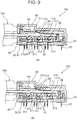
- FIG. 9 is a sectional view illustrating operations of the final stage when the insertion section of the mating connector is inserted into the connector according to the present embodiment illustrated in FIGS. 1-8 .
- Part (A) of FIG. 9 is a view illustrating a state in which the tabular insertion section 710 of the mating connector 700 is inserted up to a position slightly before the final position.
- Part (B) of the FIG. 9 is a view illustrating a state in which the insertion section 710 is inserted up to the final position.
- connection pads 711 corresponding to the contacts 10 are formed on the first surface (a surface facing the contacts 10) of the insertion section 710.
- the ground connection pad 712 is formed on a second surface (a surface facing the outer shell 50) of the insertion section 710.
- the base housing 20, the slider 30 and the upper housing 40 are stacked from a bottom to a top in this order on the circuit board (not illustrated) and are connected to the circuit board.
- the upper housing 40 is covered by the outer shell 50 so that the insertion receiving section for receiving the insertion section 710 of the mating connector 700 therein is formed.
- the contacts 10 are press-fitted into the elongated openings 211 of the base housing 20 to be held.
- the contacts 10 go through the elongated openings 311 of the slider 30, and further enter the elongated openings 411 of the upper housing 40.
- the top ends of the contacts 10 remain inside the elongated openings 411 of the upper housing 40.
- the contacts 10 are located at positions which face the insertion section 710 and also are separated from the insertion section 710 when the insertion section 710 of the mating connector 700 is inserted into the insertion receiving section.
- Cam surfaces 313 oriented obliquely upward are formed on the walls which are included in the respective elongated openings 311 of the cam plate 31 of the slider 30 and are on the rear side in the insertion direction (the left side in FIG. 9 ).
- portions positioned upper than the midpoints in the contacts 10 are deformed by the cam surfaces 313 such that the portions positioned more upward than the midpoints in the contacts 10 are lifted by the cam surfaces 313, respectively, and enter the state as illustrated in part (B) of FIG. 9 .
- the contacts 10 are pressed against the corresponding connection pads 711 which are formed on the first surface of the insertion section 710 of the mating connector 700, so that the contacts 10 are electrically conducted to the corresponding connection pads 711, respectively.
- the state is in that the spring contact pieces 68 attached to the outer shell 50 make contact with the grounding pad 712 formed on the second surface of the insertion section 710.
- the contacts 10 are pressed against the connection pads 711 at the final stage of the insertion in which the insertion section 710 of the mating connector 700 is inserted into the insertion receiving section. For this reason, until the final stage of the insertion, the insertion section 710 is inserted by a low insertion force without suffering interference from the contacts 10.
- slider 30 receives a force from the insertion section 710 of the mating connector 700 to press the contacts 10 against the connection pads 711, so that the mating is completed only by the insertion operation.
- connection pads are arranged in the insertion direction on the first surface of the insertion section 710 of the mating connector 700, and corresponding to the arrangement, the connector 100 of the present embodiment has the configuration in which the connector 100 includes the contacts 10 arranged in the insertion direction.
- the connector 100 includes the contacts 10 arranged in the insertion direction.
- the contacts 10 come into contact with the insertion section 710 including the connection pads 711 is the final stage of the insertion.
- a contact 10 which does not correspond to a corresponding connection pad 711 makes contact with the corresponding connection pad 711 at the mid-stage of the insertion to cause malfunction to occur.
- a contact pad 711 positioned more forward in the insertion direction is rubbed with a contact 10 more frequently to decrease the life thereof.
Landscapes
- Coupling Device And Connection With Printed Circuit (AREA)
- Details Of Connecting Devices For Male And Female Coupling (AREA)
Description
- The present invention relates to a connector including a contact for making contact with a connection pad of a mating connector inserted into an insertion receiving section for receiving the mating connector therein.
- There have been developed a connector including many contacts serving for transmitting plural electrical signals. Such a connector tends to be sized up as the number of contacts increases. In addition, such a connector tends to require a large mating force when the connector is mated with a mating connector.
- Regarding decreasing of the mating force, there is known a connector of low-insertion-force type having a configuration in which, after an operation for mating with a mating connector with the connector is performed, other operations such as rotating a lever and the like are performed (see, for example, Japanese Patent Publication
JP 2002-170642A - The low-insertion-force type connector can be mated with a mating connector by a small force since mating completion is performed by, for example, a lever operation and the like, and thus, the low-insertion-force type connector is suitable for one having many contacts. However, a connector of such type requires not only an operation of mating a mating connector, but also, subsequently, an operation of, for example, a lever operation and the like, and thus, requires operations two times for mating once. In addition, the connection needs to include members such as a lever member, a member for operating the lever member and the like are required, and further, an indicator for remembering a second operation (for example, a lever operation) and other schemes are also required, and thus, such connector tends to have a complicated configuration.
-
JP H09 251878 A US 2011/0021079 discloses also an electrical card connector comprising a housing including contacts, and a slider. The contacts are configured to be spaced from a first surface of an SD card when the SD card is initially inserted into an insertion receiving section of the housing by parts of the contacts resiliently engaging an inclined surface of a blocking portion of the slider. The slider has a pair of arms configured to be engaged by the SD card so that the slider is moved in the same direction as the SD card when the SD card is inserted into the connector. As the slider is moved, the blocking portion is moved away from the contacts so that the contacts spring through slots in the slider into engagement with the SD card. -
US 2002/0070274 discloses an IC card reading connector having a body containing a plurality of terminals. The body holds a movable flat block and the block has trenches for receiving the terminals which are biased towards the top side of the block on which an IC card is to rest. The movable flat block also has an IC card holding plate on its top side. The distal end of each terminal has a pair of protrusions wherein each protrusion engages an inclined guide surface on an underside of the movable flat block. When an IC card is inserted into the connector it engages the IC card holding plate so that the movable flat block moves in the same direction as the IC card. As the movable flat block moves, the distal end of the terminals engage a different part of the inclined guide surface which is closer to the top side enabling the biased terminals to engage the IC card. -
JP 2009-152144 - In view of the foregoing problems, the present invention has been made to provide a connector whose mating is completed by only one insertion operation of a mating connector, and which has a configuration suitable for including many contacts.
- A connector according to one aspect of the present invention is disclosed by claim 1 and includes: a housing including an insertion receiving section which is configured to receive a tabular insertion section of a mating connector having connection pads formed on a first surface of the insertion section; contacts configured to correspond to the connection pads, the contacts being configured to face the first surface when the insertion section of the mating connector is inserted into the insertion receiving section, and the contacts being configured to be spaced from the first surface when the insertion section is initially inserted into the insertion receiving section; and a pressing member being a slider, the slider configured to receive a force from the insertion section when the insertion section is at a final stage of insertion into the insertion receiving section, the slider including an abutment section which is configured to be engaged by the insertion section when the insertion section is inserted into the insertion receiving section so that the abutment section is moved in the same direction as the insertion section, the slider further including a cam section, the cam section being a cam plate having elongated openings through which the contacts pass, and cam surfaces formed on walls included in the respective elongated openings, characterized in that the cam plate is configured to press the contacts towards the first surface of the insertion section when the abutment section is moved so as to cause the contacts to elastically deform and be pressed against the connection pads, the cam surfaces being orientated to extend obliquely towards the first surface when the insertion section is inserted into the insertion receiving section, and the cam surfaces being on the rear side in the insertion direction of the mating connector.
- The connector according to the present invention includes the above-described pressing member, and thus, the contacts are pressed against the connection pads when moving to the final stage of inserting the mating connector into the insertion receiving section. For this reason, the insertion section does not suffer or just slightly suffers an interference from the contacts until the final stage of the insertion movement, and thus, the mating connector can be inserted by an small insertion force. As for the pressing member, since the contacts receive a force from the insertion section to be connected to the connection pad in the final stage of the insertion movement, the mating is completed by only the insertion movement.
- Since the contacts are pressed against the insertion section including the connection pads in the final stage of the insertion, there is no possibility where a pad arranged more forwardly in the insertion direction rubs against a contact more frequently for many times, and thereby preventing the life thereof from being shortened.
- As described above, due to the pressing section including the abutment section and the cam section, pressing the contacts against the connection pads in the final stage of the insertion can be obtained with a simple structure.
- According to the above-described present invention, the connector having structure suitable for having multiple contacts is provided, in which the mating is completed by only one insertion operation of the mating connector.
- According to another aspect of the present invention there is provided a method of mating connectors according to claim 2 comprising the steps of: (a) providing a mating connector having a tabular insertion section and connection pads formed on a first surface of the insertion section; (b) providing a connector having a housing that includes an insertion receiving section to receive the tabular insertion section of the mating connector, contacts which correspond to the connection pads, and a pressing member being a slider and having an abutment section and a cam section, the cam section being a cam plate and having elongated openings through which the contacts pass, and cam surfaces formed on walls included in the respective elongated openings, the cam surfaces being orientated to extend obliquely towards the first surface when the insertion section is inserted into the insertion receiving section, and the cam surfaces being on the rear side in the insertion direction of the mating connector; and (c) inserting the insertion section of the mating connector into the insertion receiving section of the connector such that the contacts face the first surface, and wherein: (i) when the insertion section is initially inserted into the insertion receiving section, the contacts are spaced from the first surface; and (ii) when the insertion section is at the final stage of insertion into the insertion receiving section, the contacts are pressed against the connection pads by means of the slider receiving a force from the insertion section, wherein the abutment section engages with the insertion section so that the abutment section is moved in the same direction as the insertion section, and the contacts are pressed towards the first surface of the insertion section by means of the cam plate when the abutment section is moved so as to cause the contacts to elastically deform and be pressed against the connection pads.
-
-
FIG. 1 is an external perspective view of a connector of an embodiment according to the present invention; -
FIG. 2 is an exploded perspective view illustrating the connector whose external view is illustrated inFIG. 1 where the connector is exploded into an outer shell (part (A)) and remaining components (part (B)); -
FIG. 3 is a perspective view illustrating the outer shell upside down; -
FIG. 4 is an exploded perspective view illustrating an assembly remained by removing the outer shell from the connector according the present embodiment where the assembly is separated into an upper housing with a lid member (part (A)) and remaining components (part (B)); -
FIG. 5 is an exploded perspective view illustrating the upper housing with the lid member where the upper housing with lid member is separated into the upper housing (part (A)) and the lid member (part (B)); -
FIG. 6 is a perspective view illustrating a base housing upside down in a state in which the contacts are press-fitted into the base housing; -
FIG. 7 is an exploded perspective view illustrating all of the components included in the connector according to the present embodiment whose assembled state is illustrated inFIG. 1 ; -
FIG. 8 is an exploded perspective view illustrating the connector illustrated inFIG. 1 upside down while all of the components are separated from each other; and -
FIG. 9 is a sectional view illustrating operations in the final stage when an insertion section of a mating connector is inserted into the connector according to the present embodiment. - In the following, an embodiment of the connector according to the present invention will be described with reference to the attached drawings.
-
FIG. 1 is an external perspective view of a connector of an embodiment according to the present invention. - The
connector 100 is covered with anouter shell 50 made of metal. An insertion opening 251 which is covered with alid member 64 and into which a tabular insertion section of a mating connector is to be inserted is provided in afront wall 25 of abase housing 20 which is exposed toward the front. -
FIG. 2 is an exploded perspective view illustrating the connector whose external view is illustrated inFIG. 1 where the connector is exploded into an outer shell (part (A)) and remaining components (part (B)). -
FIG. 3 is a perspective view illustrating the outer shell upside down. -
FIG. 4 is an exploded perspective view illustrating an assembly remained by removing the outer shell from the connector according the present embodiment where the assembly is separated into an upper housing with a lid member (part (A)) and remaining components (part (B)). -
FIG. 5 is an exploded perspective view illustrating the upper housing with the lid member where the upper housing with the lid member is separated into the upper housing (part (A)) and the lid member (part (B)). -
FIG. 6 is a perspective view illustrating a base housing upside down in a state in which the contacts are press-fitted into the base housing. -
FIG. 7 is an exploded perspective view illustrating all of the components included in the connector according to the present embodiment whose assembled state is illustrated inFIG. 1 . -
FIG. 8 is an exploded perspective view illustrating the connector illustrated inFIG. 1 upside down while all of the components are separated from each other. - Here, mainly referring to the exploded perspective views illustrated in
FIGS. 7 and8 , and also referring toFIGS. 1 to 6 as necessary, theconnector 100 will be described. - The
connector 100 according to the present embodiment includesplural contacts 10, abase housing 20, aslider 30, anupper housing 40 and anouter shell 50. - The
base housing 20 includes abottom plate 21. Manyelongated openings 211 which penetrate from a top surface through a bottom surface thereof are formed in thebottom plate 21. Thecontacts 10 are press-fitted into theelongated openings 211 from a side of a bottom surface of the bottom plate 21 (a side of thebottom surface 219 illustrated inFIG. 6 ).FIGS. 7 and8 illustrate thecontacts 10 in a state in which thecontacts 10 are press-fitted into the respectiveelongated openings 211 to be aligned. - Portions (see
FIG. 6 ) of thecontacts 10 which portions extend off from thebottom plate 21 to the side of thebottom surface 219 are to be connected to a circuit board (not illustrated) on which theconnector 100 is to be placed. - Further, as illustrated in
FIG, 7 , in addition to theelongated openings 211,grooves bottom plate 21. Acoil spring 61 is accommodated in thegroove 212 on the left, and acam member 62 in which a so-called heart cam groove is formed and acoil spring 63 are accommodated in thegroove 213 on the right. One end of acam bar 69 is inserted into the heart cam groove formed in thecam member 62. The other end of thecam bar 69 is supported by thebase housing 20. - In addition, the
base housing 20 includes arear wall 22, left andright walls front wall 25 upstanding so as to surround thebottom plate 21. - An
insertion opening 251 into which an insertion section of a mating connector is inserted is provided in thefront wall 25. Thelid member 64 which is supported by theupper housing 40 is arranged immediately inside theinsertion opening 251, thereby forming a configuration in which theinsertion opening 251 is closed by the lid member 64 (seeFIG. 1 ). Thelid member 64 has a configuration in which thelid member 64 is pressed by a tip of the insertion section of the mating connector from the outside to be rotated inwardly upward so as to open theinsertion opening 251, and when the mating connector is removed, thelid member 64 closes theinsertion opening 251 by an action of atorsion spring 65. - The
slider 30 is arranged on thebottom plate 21 of thebase housing 20 as illustrated in part (B) ofFIG. 4 . Theslider 30 includes acam plate 31 and a standingwall 32 standing at a side of a rear end of thecam plate 31. Manyelongated openings 311 which penetrate from the top surface to the bottom surface and through which thecontacts 10 are allowed to pass as illustrated in part (B) ofFIG. 4 , and anelongated opening 312 through which thecam member 62 is allowed to pass is formed in thecam plate 31. Thecam plate 31 enters a state in which thecam plate 31 is pressed toward thefront wall 25 by the twocoil springs base housing 20. Thecoil spring 61 is accommodated in thegroove 212 to directly press theslider 30 toward thefront wall 25. Theother coil spring 63 is arranged in thegroove 213 of thebase housing 20 to directly press thecam member 62. Thecam member 62 is also placed in theelongated opening 312 of theslider 30. For this reason, thecam member 62 pressed by thecoil spring 63 presses a wall of theelongated opening 312 in theslider 30, so that theslider 30 enters a state in which theslider 30 is pressed via thecam member 62 toward thefront wall 25 in thebase housing 20. - Here, in the present embodiment, the
slider 30 corresponds to an example of the pressing member according to the present invention, the standingwall 32 corresponds to an example of the abutment section according to the present invention, and thecam plate 31 corresponds to an example of the cam section according to the present invention. - Further, the
upper housing 40 illustrated in part (A) ofFIG. 4 is arranged on theslider 30, and furthermore, theouter shell 50 illustrated in part (A) ofFIG. 2 covers theupper housing 40. Theouter shell 50 is made of metal and is held at a ground potential, thereby serving for shielding theconnector 100. - The
upper housing 40 includes anupper plate 41 and afront wall 42 standing from theupper plate 41 on a front side thereof. Theupper plate 41 forms a space between theupper plate 41 and thebase plate 21 of thebase housing 20 in which space theslider 30 is disposed. Manyelongated openings 411 which allow thecontacts 10 to pass therethrough are formed in theupper plate 41, and in addition, anelongated opening 412 which allows the standingwall 32 of theslider 30 to pass therethrough is also formed in theupper plate 41. - In addition, a
bump section 621 is provided on the above-describedcam member 62, and anelongated opening 413 which allows thebump section 621 of thecam member 62 to pass therethrough is also formed in theupper plate 41 of theupper housing 40. - In addition, a receiving
slot 421 which receives the insertion section of the mating housing which is inserted from theinsertion opening 251 formed in thefront wall 25 of thebase housing 20 is formed in thefront wall 42 of theupper housing 40. In addition, as illustrated in part (A) ofFIG. 5 , a supportingsection 422 which rotatably supports thelid member 64 is provided in an upper portion of the receivingopening 421 of thefront wall 42. Thelid member 64 is supported by the supportingsection 422 as illustrated in part (A) ofFIG. 4 to be rotatable inwardly upward. Thelid member 64 is biased in a direction of closing theinsertion opening 251 of thebase housing 20 by atorsion spring 65. - The insertion section of the mating connector is inserted from the
insertion opening 251 illustrated inFIG. 1 of thebase housing 20. Next, the insertion section pushes up thelid member 64 supported by theupper housing 40 and is inserted onto theupper housing 40 of the assembly as assembled in the state as illustrated in part (B) ofFIG. 2 from the receivingopening 421 of theupper housing 40. A tip of the inserted insertion section of the mating connector first bumps against thebump section 621 of thecam member 62 to slide thecam member 62 toward the depth against the biasing of thecoil spring 63. When thecam member 62 is slid toward the depth and thebump section 621 is positioned by the standingwall 32 of theslider 30, the tip of the insertion section of the mating connector bumps against thebump section 621 of thecam member 62 and also against the standingwall 32 of theslider 30. For this reason, the tip of the insertion section slides thecam member 62 and theslider 30 together toward the depth against the biasing of the twocoil springs connector 100 according to the present embodiment, the space over theupper plate 41 of theupper housing 40, i.e., the space between theupper plate 41 and theouter shell 50 which is put over theupper plate 41 to cover theupper plate 41 corresponds to an example of the "an insertion receiving section" to receive the mating connector. - Here, top ends of the
contacts 10 have such shapes that, before the insertion section of the mating connector is inserted, the top ends of thecontacts 10 are positioned inside theelongated openings 411 which are provided in theupper plate 41 of theupper housing 40 and allows thecontacts 10 to pass therethrough, and do not protrude from the upper surface of the upper plate 41 (see part (B) ofFIG. 2 ) . In other words, before the insertion of the insertion section of the mating connector and in the beginning of the insertion, thecontacts 10 are away or spaced from the insertion section when the insertion section of the mating connector is inserted, and are arranged at positions facing the insertion section. - In addition, many connection pads whose arrangement matches that of the
contacts 10 are formed on a surface (corresponding to an example of "a first surface" according to the present invention) of the insertion section of the mating connector which surface faces theupper plate 41 of theupper housing 40. - The insertion section of the mating connector is inserted into the insertion receiving section, i.e., onto the upper surface of the
upper plate 41 of theupper housing 40, and at the time of the final movement of the insertion, the standingwall 32 of theslider 30 is pressed or engaged by the insertion section of the mating connector to be slid. Subsequently, walls of theelongated openings 311 provided in thecam plate 31 of theslider 30 press thecontacts 10 so as to deform thecontacts 10 in a direction of protruding from theelongated openings 411 of theupper plate 41 in theupper housing 40. The insertion section of the mating connector is inserted on the upper surface of theupper plate 41, and thus, thecontacts 10 are electrically connected to the connection pads formed on the bottom surface (the first surface) of the insertion section. A manner as to how thecontacts 10 are deformed by being pressed by theslider 30 will be described later. - When the insertion section of the mating connector is inserted up to the depth, and the connection pads and the
contacts 10 enter a state of being respectively connected with each other, the heart cam groove of thecam member 62 and thecam rod 69 are engaged with each other, so that thecam member 62 is locked while being slid to the depth. Since thecam member 62 enters theelongated opening 312 of thecam plate 31 of theslider 30 to slide theslider 30 together to the depth, thecam member 62 is locked and thus theslider 30 remains in a state of being slid to the depth. Aninsertion piece 661 of alock member 66 is inserted into aninsertion opening 622 of thecam member 62, and alock section 662 of thelock member 66 is engaged with a depression section (not illustrated) on a side surface of the inserted insertion section of the mating connector to lock the mating connector in the inserted state. - In addition, a
switch piece 67 is supported in thegroove 222 on a side of the rear end of thebase housing 20 by thebase housing 20. Arear end 671 of theswitch piece 67 is pressed by theslider 30 which is being slid into the depth, and acontact section 672 makes contact with theouter shell 50 to be at the potential same as the ground potential. This fact is detected by a circuit board, so that the mating between theconnector 100 and the mating connector is recognized. - As illustrated in
FIG. 3 , thespring contact pieces 68 made of metal are attached to an inner surface of theouter shell 50. A ground pad spreads on a surface of the insertion section of the mating connector which surface faces theouter shell 50. Thespring contact pieces 68 are connected to a ground pad of the insertion section inserted into the insertion receiving section (the space defined by theupper plate 41 of theupper housing 40 and the outer shell 50), and serve for keeping the ground pad in the ground potential. - When the mating connector is pressed again toward the depth in the insertion direction in the state in which the insertion section of the mating connector is inserted into the insertion receiving section, the engagement between the heart cam groove of the
cam member 62 and acam rod 69 is released. For this reason, theslider 30 is slid forward by the biasing of the twocoil springs cam member 62 is also slid forward, so that the locking of the insertion section by thelock member 66 which locks the insertion section of the mating connector is also released. In such way, the mating connector is pressed out from theconnector 100. -
FIG. 9 is a sectional view illustrating operations of the final stage when the insertion section of the mating connector is inserted into the connector according to the present embodiment illustrated inFIGS. 1-8 . - Part (A) of
FIG. 9 is a view illustrating a state in which thetabular insertion section 710 of themating connector 700 is inserted up to a position slightly before the final position. Part (B) of theFIG. 9 is a view illustrating a state in which theinsertion section 710 is inserted up to the final position. - The
insertion section 710 of themating connector 700 is tabular, andconnection pads 711 corresponding to thecontacts 10 are formed on the first surface (a surface facing the contacts 10) of theinsertion section 710. In addition, the ground connection pad 712 is formed on a second surface (a surface facing the outer shell 50) of theinsertion section 710. - As described above, in the
connector 100 according to the present embodiment, thebase housing 20, theslider 30 and theupper housing 40 are stacked from a bottom to a top in this order on the circuit board (not illustrated) and are connected to the circuit board. Theupper housing 40 is covered by theouter shell 50 so that the insertion receiving section for receiving theinsertion section 710 of themating connector 700 therein is formed. - The
contacts 10 are press-fitted into theelongated openings 211 of thebase housing 20 to be held. Thecontacts 10 go through theelongated openings 311 of theslider 30, and further enter theelongated openings 411 of theupper housing 40. However, as illustrated in part (A) ofFIG. 9 , before the insertion and at the beginning of the insertion of theinsertion section 710 of themating connector 700, the top ends of thecontacts 10 remain inside theelongated openings 411 of theupper housing 40. In other words, before the insertion and at the beginning of the insertion, thecontacts 10 are located at positions which face theinsertion section 710 and also are separated from theinsertion section 710 when theinsertion section 710 of themating connector 700 is inserted into the insertion receiving section. Cam surfaces 313 oriented obliquely upward are formed on the walls which are included in the respectiveelongated openings 311 of thecam plate 31 of theslider 30 and are on the rear side in the insertion direction (the left side inFIG. 9 ). When theslider 30 is pressed by a tip of theinsertion section 710 of themating connector 700 and slid to the depth, as illustrated in part (A) ofFIG. 9 , the cam surfaces 313 bump midpoints of thecontacts 10, respectively. As a result, in the course in which theinsertion section 710 of themating connector 700 is further being inserted to the depth, portions positioned upper than the midpoints in thecontacts 10 are deformed by the cam surfaces 313 such that the portions positioned more upward than the midpoints in thecontacts 10 are lifted by the cam surfaces 313, respectively, and enter the state as illustrated in part (B) ofFIG. 9 . At this moment, thecontacts 10 are pressed against thecorresponding connection pads 711 which are formed on the first surface of theinsertion section 710 of themating connector 700, so that thecontacts 10 are electrically conducted to thecorresponding connection pads 711, respectively. In addition, the state is in that thespring contact pieces 68 attached to theouter shell 50 make contact with the grounding pad 712 formed on the second surface of theinsertion section 710. - As described above, according to the
connector 100 of the present embodiment, thecontacts 10 are pressed against theconnection pads 711 at the final stage of the insertion in which theinsertion section 710 of themating connector 700 is inserted into the insertion receiving section. For this reason, until the final stage of the insertion, theinsertion section 710 is inserted by a low insertion force without suffering interference from thecontacts 10. In addition,slider 30 receives a force from theinsertion section 710 of themating connector 700 to press thecontacts 10 against theconnection pads 711, so that the mating is completed only by the insertion operation. - Further, the plural connection pads are arranged in the insertion direction on the first surface of the
insertion section 710 of themating connector 700, and corresponding to the arrangement, theconnector 100 of the present embodiment has the configuration in which theconnector 100 includes thecontacts 10 arranged in the insertion direction. However, when thecontacts 10 come into contact with theinsertion section 710 including theconnection pads 711 is the final stage of the insertion. For this reason, there is no risk in which acontact 10 which does not correspond to acorresponding connection pad 711 makes contact with thecorresponding connection pad 711 at the mid-stage of the insertion to cause malfunction to occur. In addition, there is no possibility in which acontact pad 711 positioned more forward in the insertion direction is rubbed with acontact 10 more frequently to decrease the life thereof. - However, in a case in which, thanks to an idea for circuitry and the like, even if a contact which does not correspond to a corresponding connection pad makes contact with the corresponding connection pad in the middle of the insertion, malfunction does not occur, a configuration in which the
contacts 10 slightly protrude from theupper plate 41 of theupper housing 40 and the insertion section is inserted while the insertion section of the mating connector slightly makes contact with the contacts.
Claims (2)
- A connector (100) comprising: a housing (20, 40) including an insertion receiving section which is configured to receive a tabular insertion section (710) of a mating connector (700) having connection pads (711) formed on a first surface of the insertion section (710); contacts (10) configured to correspond to the connection pads (711), the contacts (10) being configured to face the first surface when the insertion section (710) of the mating connector (700) is inserted into the insertion receiving section, and the contacts (10) being configured to be spaced from the first surface when the insertion section (710) is initially inserted into the insertion receiving section; and a pressing member (30) being a slider, the slider (30) configured to receive a force from the insertion section (710) when the insertion section (710) is at a final stage of insertion into the insertion receiving section, the slider (30) including an abutment section (32) which is configured to be engaged by the insertion section (710) when the insertion section (710) is inserted into the insertion receiving section so that the abutment section (32) is moved in the same direction as the insertion section (710), the slider (30) further including a cam section (31), the cam section being a cam plate (31) wherein
the cam plate (31) is configured to press the contacts (10) towards the first surface of the insertion section (710) when the abutment section (32) is moved so as to cause the contacts (10) to elastically deform and be pressed against the connection pads (711), characterized by
the cam plate (31) having elongated openings (311) through which the contacts (10) pass, and cam surfaces (313) formed on walls included in the respective elongated openings (311), the cam surfaces (313) being orientated to extend obliquely towards the first surface when the insertion section (710) is inserted into the insertion receiving section, and the cam surfaces (313) being on the rear side in the insertion direction of the mating connector (700). - A method of mating connectors comprising the steps of:(a) providing a mating connector (700) having a tabular insertion section (710) and connection pads (711) formed on a first surface of the insertion section (710);(b) providing a connector (100) having a housing (20, 40) that includes an insertion receiving section to receive the tabular insertion section (710) of the mating connector (700), contacts (10) which correspond to the connection pads (711), and a pressing member (30) being a slider and having an abutment section (32) and a cam section (31), the cam section (31) being a cam plate and having elongated openings (311) through which the contacts (10) pass, and cam surfaces (313) formed on walls included in the respective elongated openings (311), the cam surfaces (313) being orientated to extend obliquely towards the first surface when the insertion section (710) is inserted into the insertion receiving section, and the cam surfaces (313) being on the rear side in the insertion direction of the mating connector (700); and(c) inserting the insertion section (710) of the mating connector (700) into the insertion receiving section of the connector (100) such that the contacts (10) face the first surface, and wherein: (i) when the insertion section (710) is initially inserted into the insertion receiving section, the contacts (10) are spaced from the first surface; and (ii) when the insertion section (710) is at the final stage of insertion into the insertion receiving section, the contacts (10) are pressed against the connection pads (711) by means of the slider (30) receiving a force from the insertion section (710), wherein the abutment section (32) engages with the insertion section (710) so that the abutment section (32) is moved in the same direction as the insertion section (710), and the contacts (10) are pressed towards the first surface of the insertion section (710) by means of the cam plate (31) when the abutment section (32) is moved so as to cause the contacts (10) to elastically deform and be pressed against the connection pads (711).
Applications Claiming Priority (1)
| Application Number | Priority Date | Filing Date | Title |
|---|---|---|---|
| JP2012246246A JP6000811B2 (en) | 2012-11-08 | 2012-11-08 | connector |
Publications (2)
| Publication Number | Publication Date |
|---|---|
| EP2731199A1 EP2731199A1 (en) | 2014-05-14 |
| EP2731199B1 true EP2731199B1 (en) | 2019-09-25 |
Family
ID=49518860
Family Applications (1)
| Application Number | Title | Priority Date | Filing Date |
|---|---|---|---|
| EP13191896.3A Active EP2731199B1 (en) | 2012-11-08 | 2013-11-07 | Connector |
Country Status (5)
| Country | Link |
|---|---|
| US (1) | US9780473B2 (en) |
| EP (1) | EP2731199B1 (en) |
| JP (1) | JP6000811B2 (en) |
| KR (1) | KR102041924B1 (en) |
| CN (1) | CN103811935B (en) |
Families Citing this family (8)
| Publication number | Priority date | Publication date | Assignee | Title |
|---|---|---|---|---|
| JP6215125B2 (en) * | 2014-04-21 | 2017-10-18 | 日本航空電子工業株式会社 | connector |
| JP1545402S (en) * | 2015-04-28 | 2016-03-14 | ||
| JP6524465B2 (en) * | 2015-04-28 | 2019-06-05 | タイコエレクトロニクスジャパン合同会社 | connector |
| WO2018190633A1 (en) | 2017-04-12 | 2018-10-18 | 주식회사케미텍 | Low insertion force connector assembly and semiconductor component test apparatus |
| US10916903B2 (en) | 2018-02-04 | 2021-02-09 | Creganna Unlimited Company | System having a cable assembly and plug and receptacle connectors |
| US10418734B1 (en) | 2018-07-26 | 2019-09-17 | Te Connectivity Corporation | Contact assembly for a straddle mount connector |
| US10559920B1 (en) | 2018-08-07 | 2020-02-11 | Te Connectivity Corporation | Card edge connector having improved mating interface |
| JP7316192B2 (en) * | 2019-10-29 | 2023-07-27 | タイコエレクトロニクスジャパン合同会社 | socket |
Citations (3)
| Publication number | Priority date | Publication date | Assignee | Title |
|---|---|---|---|---|
| DE4010398A1 (en) * | 1990-03-31 | 1991-10-10 | Stocko Metallwarenfab Henkels | DEVICE FOR ELECTRICALLY CONTACTING AN IC MEMORY CARD WITH AN ELECTRONIC DEVICE |
| JPH09251878A (en) * | 1996-03-14 | 1997-09-22 | Tamura Electric Works Ltd | Ic card connector |
| US20110021079A1 (en) * | 2009-07-23 | 2011-01-27 | Hon Hai Precision Industry Co., Ltd. | Electrical card connector |
Family Cites Families (11)
| Publication number | Priority date | Publication date | Assignee | Title |
|---|---|---|---|---|
| JPH054705Y2 (en) * | 1987-10-06 | 1993-02-05 | ||
| US4936790A (en) * | 1989-04-28 | 1990-06-26 | Apple Computer, Inc. | Low insertion force connector |
| DE4336192A1 (en) * | 1993-10-23 | 1995-05-04 | Thomas & Betts Gmbh | Reader for chip cards |
| US5679018A (en) * | 1996-04-17 | 1997-10-21 | Molex Incorporated | Circuit card connector utilizing flexible film circuitry |
| US5750973A (en) | 1996-10-31 | 1998-05-12 | The Whitaker Corporation | Card reader |
| JP2001203048A (en) * | 2000-01-20 | 2001-07-27 | Fujitsu Takamisawa Component Ltd | Connector and electronic components |
| JP3710705B2 (en) | 2000-11-30 | 2005-10-26 | タイコエレクトロニクスアンプ株式会社 | Low insertion force connector |
| US20020070274A1 (en) | 2000-12-11 | 2002-06-13 | Tien-Tsai Lee | IC card reading connector |
| US6796842B1 (en) * | 2003-10-08 | 2004-09-28 | Ming-Te Wang | Electronic card connector |
| US7044797B1 (en) * | 2005-01-26 | 2006-05-16 | Taisol Electronics Co., Ltd. | Memory card connector |
| JP4973485B2 (en) * | 2007-12-21 | 2012-07-11 | 日本電気株式会社 | connector |
-
2012
- 2012-11-08 JP JP2012246246A patent/JP6000811B2/en active Active
-
2013
- 2013-11-06 KR KR1020130134132A patent/KR102041924B1/en active IP Right Grant
- 2013-11-07 EP EP13191896.3A patent/EP2731199B1/en active Active
- 2013-11-08 US US14/075,221 patent/US9780473B2/en active Active
- 2013-11-08 CN CN201310550013.1A patent/CN103811935B/en active Active
Patent Citations (3)
| Publication number | Priority date | Publication date | Assignee | Title |
|---|---|---|---|---|
| DE4010398A1 (en) * | 1990-03-31 | 1991-10-10 | Stocko Metallwarenfab Henkels | DEVICE FOR ELECTRICALLY CONTACTING AN IC MEMORY CARD WITH AN ELECTRONIC DEVICE |
| JPH09251878A (en) * | 1996-03-14 | 1997-09-22 | Tamura Electric Works Ltd | Ic card connector |
| US20110021079A1 (en) * | 2009-07-23 | 2011-01-27 | Hon Hai Precision Industry Co., Ltd. | Electrical card connector |
Also Published As
| Publication number | Publication date |
|---|---|
| US9780473B2 (en) | 2017-10-03 |
| JP2014096249A (en) | 2014-05-22 |
| KR20140059736A (en) | 2014-05-16 |
| EP2731199A1 (en) | 2014-05-14 |
| US20140127922A1 (en) | 2014-05-08 |
| CN103811935A (en) | 2014-05-21 |
| CN103811935B (en) | 2017-09-22 |
| KR102041924B1 (en) | 2019-11-07 |
| JP6000811B2 (en) | 2016-10-05 |
Similar Documents
| Publication | Publication Date | Title |
|---|---|---|
| EP2731199B1 (en) | Connector | |
| JP4385047B2 (en) | Contact and card adapter and card connector provided therewith | |
| US7717724B2 (en) | Connector card housing with a slider restraining protrusion | |
| US8740634B2 (en) | Card connector | |
| US20110003496A1 (en) | Card connector with switch element | |
| TWI398044B (en) | Card connector | |
| US6767232B1 (en) | Electrical card connector having write-protect and full-insertion switches | |
| US7238034B2 (en) | Memory card connector | |
| US7374440B2 (en) | Card connector with metal shell | |
| KR100999873B1 (en) | Memory card connector | |
| US8851911B2 (en) | Card connector | |
| US6929491B1 (en) | Card connector | |
| US20120058657A1 (en) | Electrical card connector having detecting contacts actuated by slider | |
| US20060205278A1 (en) | Electrical card connector | |
| US7238052B2 (en) | Card connector with anti-mismating device | |
| WO2004032289A1 (en) | Memory card connector | |
| US20070149017A1 (en) | Card connector with an ejector | |
| US20120244734A1 (en) | Card edge connector with floatable grounding pads | |
| US7549876B2 (en) | Electrical card connector having an insulative housing integrally molded with a shell | |
| JP2004349223A (en) | Socket for memory card | |
| US7214098B2 (en) | Memory card connector | |
| KR101361740B1 (en) | Dual card type socket and assembly method thereof | |
| US20060134947A1 (en) | Electrical card connector with protective device | |
| US7275944B1 (en) | Card connector capable of detecting insertion of card | |
| US8251726B2 (en) | Electrical connector having a metal frame with locking portions movable in transverse direction for locking/unlocking a card |
Legal Events
| Date | Code | Title | Description |
|---|---|---|---|
| PUAI | Public reference made under article 153(3) epc to a published international application that has entered the european phase |
Free format text: ORIGINAL CODE: 0009012 |
|
| 17P | Request for examination filed |
Effective date: 20131107 |
|
| AK | Designated contracting states |
Kind code of ref document: A1 Designated state(s): AL AT BE BG CH CY CZ DE DK EE ES FI FR GB GR HR HU IE IS IT LI LT LU LV MC MK MT NL NO PL PT RO RS SE SI SK SM TR |
|
| AX | Request for extension of the european patent |
Extension state: BA ME |
|
| R17P | Request for examination filed (corrected) |
Effective date: 20141013 |
|
| RBV | Designated contracting states (corrected) |
Designated state(s): AL AT BE BG CH CY CZ DE DK EE ES FI FR GB GR HR HU IE IS IT LI LT LU LV MC MK MT NL NO PL PT RO RS SE SI SK SM TR |
|
| 17Q | First examination report despatched |
Effective date: 20160302 |
|
| STAA | Information on the status of an ep patent application or granted ep patent |
Free format text: STATUS: EXAMINATION IS IN PROGRESS |
|
| GRAP | Despatch of communication of intention to grant a patent |
Free format text: ORIGINAL CODE: EPIDOSNIGR1 |
|
| STAA | Information on the status of an ep patent application or granted ep patent |
Free format text: STATUS: GRANT OF PATENT IS INTENDED |
|
| RIC1 | Information provided on ipc code assigned before grant |
Ipc: H01R 12/89 20110101AFI20190326BHEP Ipc: H01R 13/24 20060101ALN20190326BHEP |
|
| INTG | Intention to grant announced |
Effective date: 20190418 |
|
| GRAS | Grant fee paid |
Free format text: ORIGINAL CODE: EPIDOSNIGR3 |
|
| GRAA | (expected) grant |
Free format text: ORIGINAL CODE: 0009210 |
|
| STAA | Information on the status of an ep patent application or granted ep patent |
Free format text: STATUS: THE PATENT HAS BEEN GRANTED |
|
| AK | Designated contracting states |
Kind code of ref document: B1 Designated state(s): AL AT BE BG CH CY CZ DE DK EE ES FI FR GB GR HR HU IE IS IT LI LT LU LV MC MK MT NL NO PL PT RO RS SE SI SK SM TR |
|
| REG | Reference to a national code |
Ref country code: GB Ref legal event code: FG4D |
|
| REG | Reference to a national code |
Ref country code: CH Ref legal event code: EP |
|
| REG | Reference to a national code |
Ref country code: AT Ref legal event code: REF Ref document number: 1184743 Country of ref document: AT Kind code of ref document: T Effective date: 20191015 |
|
| REG | Reference to a national code |
Ref country code: IE Ref legal event code: FG4D |
|
| REG | Reference to a national code |
Ref country code: DE Ref legal event code: R096 Ref document number: 602013060900 Country of ref document: DE |
|
| REG | Reference to a national code |
Ref country code: NL Ref legal event code: FP |
|
| PG25 | Lapsed in a contracting state [announced via postgrant information from national office to epo] |
Ref country code: FI Free format text: LAPSE BECAUSE OF FAILURE TO SUBMIT A TRANSLATION OF THE DESCRIPTION OR TO PAY THE FEE WITHIN THE PRESCRIBED TIME-LIMIT Effective date: 20190925 Ref country code: NO Free format text: LAPSE BECAUSE OF FAILURE TO SUBMIT A TRANSLATION OF THE DESCRIPTION OR TO PAY THE FEE WITHIN THE PRESCRIBED TIME-LIMIT Effective date: 20191225 Ref country code: SE Free format text: LAPSE BECAUSE OF FAILURE TO SUBMIT A TRANSLATION OF THE DESCRIPTION OR TO PAY THE FEE WITHIN THE PRESCRIBED TIME-LIMIT Effective date: 20190925 Ref country code: LT Free format text: LAPSE BECAUSE OF FAILURE TO SUBMIT A TRANSLATION OF THE DESCRIPTION OR TO PAY THE FEE WITHIN THE PRESCRIBED TIME-LIMIT Effective date: 20190925 Ref country code: HR Free format text: LAPSE BECAUSE OF FAILURE TO SUBMIT A TRANSLATION OF THE DESCRIPTION OR TO PAY THE FEE WITHIN THE PRESCRIBED TIME-LIMIT Effective date: 20190925 Ref country code: BG Free format text: LAPSE BECAUSE OF FAILURE TO SUBMIT A TRANSLATION OF THE DESCRIPTION OR TO PAY THE FEE WITHIN THE PRESCRIBED TIME-LIMIT Effective date: 20191225 |
|
| REG | Reference to a national code |
Ref country code: LT Ref legal event code: MG4D |
|
| PG25 | Lapsed in a contracting state [announced via postgrant information from national office to epo] |
Ref country code: LV Free format text: LAPSE BECAUSE OF FAILURE TO SUBMIT A TRANSLATION OF THE DESCRIPTION OR TO PAY THE FEE WITHIN THE PRESCRIBED TIME-LIMIT Effective date: 20190925 Ref country code: RS Free format text: LAPSE BECAUSE OF FAILURE TO SUBMIT A TRANSLATION OF THE DESCRIPTION OR TO PAY THE FEE WITHIN THE PRESCRIBED TIME-LIMIT Effective date: 20190925 Ref country code: GR Free format text: LAPSE BECAUSE OF FAILURE TO SUBMIT A TRANSLATION OF THE DESCRIPTION OR TO PAY THE FEE WITHIN THE PRESCRIBED TIME-LIMIT Effective date: 20191226 |
|
| REG | Reference to a national code |
Ref country code: AT Ref legal event code: MK05 Ref document number: 1184743 Country of ref document: AT Kind code of ref document: T Effective date: 20190925 |
|
| PG25 | Lapsed in a contracting state [announced via postgrant information from national office to epo] |
Ref country code: IT Free format text: LAPSE BECAUSE OF FAILURE TO SUBMIT A TRANSLATION OF THE DESCRIPTION OR TO PAY THE FEE WITHIN THE PRESCRIBED TIME-LIMIT Effective date: 20190925 Ref country code: RO Free format text: LAPSE BECAUSE OF FAILURE TO SUBMIT A TRANSLATION OF THE DESCRIPTION OR TO PAY THE FEE WITHIN THE PRESCRIBED TIME-LIMIT Effective date: 20190925 Ref country code: PT Free format text: LAPSE BECAUSE OF FAILURE TO SUBMIT A TRANSLATION OF THE DESCRIPTION OR TO PAY THE FEE WITHIN THE PRESCRIBED TIME-LIMIT Effective date: 20200127 Ref country code: ES Free format text: LAPSE BECAUSE OF FAILURE TO SUBMIT A TRANSLATION OF THE DESCRIPTION OR TO PAY THE FEE WITHIN THE PRESCRIBED TIME-LIMIT Effective date: 20190925 Ref country code: PL Free format text: LAPSE BECAUSE OF FAILURE TO SUBMIT A TRANSLATION OF THE DESCRIPTION OR TO PAY THE FEE WITHIN THE PRESCRIBED TIME-LIMIT Effective date: 20190925 Ref country code: AT Free format text: LAPSE BECAUSE OF FAILURE TO SUBMIT A TRANSLATION OF THE DESCRIPTION OR TO PAY THE FEE WITHIN THE PRESCRIBED TIME-LIMIT Effective date: 20190925 Ref country code: AL Free format text: LAPSE BECAUSE OF FAILURE TO SUBMIT A TRANSLATION OF THE DESCRIPTION OR TO PAY THE FEE WITHIN THE PRESCRIBED TIME-LIMIT Effective date: 20190925 Ref country code: EE Free format text: LAPSE BECAUSE OF FAILURE TO SUBMIT A TRANSLATION OF THE DESCRIPTION OR TO PAY THE FEE WITHIN THE PRESCRIBED TIME-LIMIT Effective date: 20190925 |
|
| PG25 | Lapsed in a contracting state [announced via postgrant information from national office to epo] |
Ref country code: CZ Free format text: LAPSE BECAUSE OF FAILURE TO SUBMIT A TRANSLATION OF THE DESCRIPTION OR TO PAY THE FEE WITHIN THE PRESCRIBED TIME-LIMIT Effective date: 20190925 Ref country code: SM Free format text: LAPSE BECAUSE OF FAILURE TO SUBMIT A TRANSLATION OF THE DESCRIPTION OR TO PAY THE FEE WITHIN THE PRESCRIBED TIME-LIMIT Effective date: 20190925 Ref country code: SK Free format text: LAPSE BECAUSE OF FAILURE TO SUBMIT A TRANSLATION OF THE DESCRIPTION OR TO PAY THE FEE WITHIN THE PRESCRIBED TIME-LIMIT Effective date: 20190925 Ref country code: IS Free format text: LAPSE BECAUSE OF FAILURE TO SUBMIT A TRANSLATION OF THE DESCRIPTION OR TO PAY THE FEE WITHIN THE PRESCRIBED TIME-LIMIT Effective date: 20200224 |
|
| REG | Reference to a national code |
Ref country code: DE Ref legal event code: R097 Ref document number: 602013060900 Country of ref document: DE |
|
| REG | Reference to a national code |
Ref country code: CH Ref legal event code: PL |
|
| PG2D | Information on lapse in contracting state deleted |
Ref country code: IS |
|
| PG25 | Lapsed in a contracting state [announced via postgrant information from national office to epo] |
Ref country code: DK Free format text: LAPSE BECAUSE OF FAILURE TO SUBMIT A TRANSLATION OF THE DESCRIPTION OR TO PAY THE FEE WITHIN THE PRESCRIBED TIME-LIMIT Effective date: 20190925 Ref country code: MC Free format text: LAPSE BECAUSE OF FAILURE TO SUBMIT A TRANSLATION OF THE DESCRIPTION OR TO PAY THE FEE WITHIN THE PRESCRIBED TIME-LIMIT Effective date: 20190925 Ref country code: LI Free format text: LAPSE BECAUSE OF NON-PAYMENT OF DUE FEES Effective date: 20191130 Ref country code: CH Free format text: LAPSE BECAUSE OF NON-PAYMENT OF DUE FEES Effective date: 20191130 Ref country code: LU Free format text: LAPSE BECAUSE OF NON-PAYMENT OF DUE FEES Effective date: 20191107 Ref country code: IS Free format text: LAPSE BECAUSE OF FAILURE TO SUBMIT A TRANSLATION OF THE DESCRIPTION OR TO PAY THE FEE WITHIN THE PRESCRIBED TIME-LIMIT Effective date: 20200126 |
|
| PLBE | No opposition filed within time limit |
Free format text: ORIGINAL CODE: 0009261 |
|
| STAA | Information on the status of an ep patent application or granted ep patent |
Free format text: STATUS: NO OPPOSITION FILED WITHIN TIME LIMIT |
|
| REG | Reference to a national code |
Ref country code: BE Ref legal event code: MM Effective date: 20191130 |
|
| 26N | No opposition filed |
Effective date: 20200626 |
|
| GBPC | Gb: european patent ceased through non-payment of renewal fee |
Effective date: 20191225 |
|
| PG25 | Lapsed in a contracting state [announced via postgrant information from national office to epo] |
Ref country code: FR Free format text: LAPSE BECAUSE OF NON-PAYMENT OF DUE FEES Effective date: 20191125 Ref country code: GB Free format text: LAPSE BECAUSE OF NON-PAYMENT OF DUE FEES Effective date: 20191225 |
|
| PG25 | Lapsed in a contracting state [announced via postgrant information from national office to epo] |
Ref country code: BE Free format text: LAPSE BECAUSE OF NON-PAYMENT OF DUE FEES Effective date: 20191130 Ref country code: SI Free format text: LAPSE BECAUSE OF FAILURE TO SUBMIT A TRANSLATION OF THE DESCRIPTION OR TO PAY THE FEE WITHIN THE PRESCRIBED TIME-LIMIT Effective date: 20190925 |
|
| PG25 | Lapsed in a contracting state [announced via postgrant information from national office to epo] |
Ref country code: CY Free format text: LAPSE BECAUSE OF FAILURE TO SUBMIT A TRANSLATION OF THE DESCRIPTION OR TO PAY THE FEE WITHIN THE PRESCRIBED TIME-LIMIT Effective date: 20190925 |
|
| PG25 | Lapsed in a contracting state [announced via postgrant information from national office to epo] |
Ref country code: HU Free format text: LAPSE BECAUSE OF FAILURE TO SUBMIT A TRANSLATION OF THE DESCRIPTION OR TO PAY THE FEE WITHIN THE PRESCRIBED TIME-LIMIT; INVALID AB INITIO Effective date: 20131107 Ref country code: MT Free format text: LAPSE BECAUSE OF FAILURE TO SUBMIT A TRANSLATION OF THE DESCRIPTION OR TO PAY THE FEE WITHIN THE PRESCRIBED TIME-LIMIT Effective date: 20190925 |
|
| PG25 | Lapsed in a contracting state [announced via postgrant information from national office to epo] |
Ref country code: TR Free format text: LAPSE BECAUSE OF FAILURE TO SUBMIT A TRANSLATION OF THE DESCRIPTION OR TO PAY THE FEE WITHIN THE PRESCRIBED TIME-LIMIT Effective date: 20190925 |
|
| PG25 | Lapsed in a contracting state [announced via postgrant information from national office to epo] |
Ref country code: MK Free format text: LAPSE BECAUSE OF FAILURE TO SUBMIT A TRANSLATION OF THE DESCRIPTION OR TO PAY THE FEE WITHIN THE PRESCRIBED TIME-LIMIT Effective date: 20190925 |
|
| PGFP | Annual fee paid to national office [announced via postgrant information from national office to epo] |
Ref country code: NL Payment date: 20230915 Year of fee payment: 11 Ref country code: IE Payment date: 20230912 Year of fee payment: 11 |
|
| PGFP | Annual fee paid to national office [announced via postgrant information from national office to epo] |
Ref country code: DE Payment date: 20230912 Year of fee payment: 11 |